EP3032632B1 - Secondary battery and method for manufacturing same - Google Patents
Secondary battery and method for manufacturing same Download PDFInfo
- Publication number
- EP3032632B1 EP3032632B1 EP13891018.7A EP13891018A EP3032632B1 EP 3032632 B1 EP3032632 B1 EP 3032632B1 EP 13891018 A EP13891018 A EP 13891018A EP 3032632 B1 EP3032632 B1 EP 3032632B1
- Authority
- EP
- European Patent Office
- Prior art keywords
- active material
- electrode
- positive
- thickness
- current collector
- Prior art date
- Legal status (The legal status is an assumption and is not a legal conclusion. Google has not performed a legal analysis and makes no representation as to the accuracy of the status listed.)
- Active
Links
- 238000004519 manufacturing process Methods 0.000 title claims description 27
- 238000000034 method Methods 0.000 title claims description 15
- 239000007774 positive electrode material Substances 0.000 claims description 112
- 239000011810 insulating material Substances 0.000 claims description 76
- 239000011149 active material Substances 0.000 claims description 57
- 239000007773 negative electrode material Substances 0.000 claims description 36
- 230000007423 decrease Effects 0.000 claims description 13
- 239000000463 material Substances 0.000 description 17
- 239000002002 slurry Substances 0.000 description 17
- 229920005989 resin Polymers 0.000 description 14
- 239000011347 resin Substances 0.000 description 14
- 238000000576 coating method Methods 0.000 description 13
- 239000011248 coating agent Substances 0.000 description 11
- 238000005520 cutting process Methods 0.000 description 11
- -1 LiNi(1-x)CoO2 Inorganic materials 0.000 description 9
- HBBGRARXTFLTSG-UHFFFAOYSA-N Lithium ion Chemical compound [Li+] HBBGRARXTFLTSG-UHFFFAOYSA-N 0.000 description 8
- 229910001416 lithium ion Inorganic materials 0.000 description 8
- 238000010586 diagram Methods 0.000 description 7
- 239000003792 electrolyte Substances 0.000 description 7
- OKTJSMMVPCPJKN-UHFFFAOYSA-N Carbon Chemical compound [C] OKTJSMMVPCPJKN-UHFFFAOYSA-N 0.000 description 6
- 239000011230 binding agent Substances 0.000 description 6
- 239000004743 Polypropylene Substances 0.000 description 5
- 229910052782 aluminium Inorganic materials 0.000 description 5
- XAGFODPZIPBFFR-UHFFFAOYSA-N aluminium Chemical compound [Al] XAGFODPZIPBFFR-UHFFFAOYSA-N 0.000 description 5
- 230000015572 biosynthetic process Effects 0.000 description 5
- 229920001155 polypropylene Polymers 0.000 description 5
- RYGMFSIKBFXOCR-UHFFFAOYSA-N Copper Chemical compound [Cu] RYGMFSIKBFXOCR-UHFFFAOYSA-N 0.000 description 4
- PXHVJJICTQNCMI-UHFFFAOYSA-N Nickel Chemical compound [Ni] PXHVJJICTQNCMI-UHFFFAOYSA-N 0.000 description 4
- GWEVSGVZZGPLCZ-UHFFFAOYSA-N Titan oxide Chemical compound O=[Ti]=O GWEVSGVZZGPLCZ-UHFFFAOYSA-N 0.000 description 4
- 239000003795 chemical substances by application Substances 0.000 description 4
- 150000001875 compounds Chemical class 0.000 description 4
- 230000000694 effects Effects 0.000 description 4
- 239000003960 organic solvent Substances 0.000 description 4
- 229920002981 polyvinylidene fluoride Polymers 0.000 description 4
- 229910002097 Lithium manganese(III,IV) oxide Inorganic materials 0.000 description 3
- 239000000956 alloy Substances 0.000 description 3
- 239000006229 carbon black Substances 0.000 description 3
- 230000000052 comparative effect Effects 0.000 description 3
- 229910052802 copper Inorganic materials 0.000 description 3
- 239000010949 copper Substances 0.000 description 3
- 230000006866 deterioration Effects 0.000 description 3
- 229910002804 graphite Inorganic materials 0.000 description 3
- 239000010439 graphite Substances 0.000 description 3
- 230000001965 increasing effect Effects 0.000 description 3
- 239000010954 inorganic particle Substances 0.000 description 3
- 229910052751 metal Inorganic materials 0.000 description 3
- 239000002184 metal Substances 0.000 description 3
- 239000000203 mixture Substances 0.000 description 3
- 229920000098 polyolefin Polymers 0.000 description 3
- 239000010935 stainless steel Substances 0.000 description 3
- 229910001220 stainless steel Inorganic materials 0.000 description 3
- YEJRWHAVMIAJKC-UHFFFAOYSA-N 4-Butyrolactone Chemical compound O=C1CCCO1 YEJRWHAVMIAJKC-UHFFFAOYSA-N 0.000 description 2
- 229910000881 Cu alloy Inorganic materials 0.000 description 2
- OIFBSDVPJOWBCH-UHFFFAOYSA-N Diethyl carbonate Chemical compound CCOC(=O)OCC OIFBSDVPJOWBCH-UHFFFAOYSA-N 0.000 description 2
- PPBRXRYQALVLMV-UHFFFAOYSA-N Styrene Chemical compound C=CC1=CC=CC=C1 PPBRXRYQALVLMV-UHFFFAOYSA-N 0.000 description 2
- RTAQQCXQSZGOHL-UHFFFAOYSA-N Titanium Chemical compound [Ti] RTAQQCXQSZGOHL-UHFFFAOYSA-N 0.000 description 2
- 229910045601 alloy Inorganic materials 0.000 description 2
- 229910052799 carbon Inorganic materials 0.000 description 2
- 230000015556 catabolic process Effects 0.000 description 2
- 239000006258 conductive agent Substances 0.000 description 2
- 230000003247 decreasing effect Effects 0.000 description 2
- 238000006731 degradation reaction Methods 0.000 description 2
- 230000001419 dependent effect Effects 0.000 description 2
- VUPKGFBOKBGHFZ-UHFFFAOYSA-N dipropyl carbonate Chemical compound CCCOC(=O)OCCC VUPKGFBOKBGHFZ-UHFFFAOYSA-N 0.000 description 2
- 238000001035 drying Methods 0.000 description 2
- JBTWLSYIZRCDFO-UHFFFAOYSA-N ethyl methyl carbonate Chemical compound CCOC(=O)OC JBTWLSYIZRCDFO-UHFFFAOYSA-N 0.000 description 2
- 238000011156 evaluation Methods 0.000 description 2
- 239000012982 microporous membrane Substances 0.000 description 2
- 229910052759 nickel Inorganic materials 0.000 description 2
- ZKATWMILCYLAPD-UHFFFAOYSA-N niobium pentoxide Chemical compound O=[Nb](=O)O[Nb](=O)=O ZKATWMILCYLAPD-UHFFFAOYSA-N 0.000 description 2
- 239000011255 nonaqueous electrolyte Substances 0.000 description 2
- 239000010450 olivine Substances 0.000 description 2
- 229910052609 olivine Inorganic materials 0.000 description 2
- 230000002093 peripheral effect Effects 0.000 description 2
- 239000010936 titanium Substances 0.000 description 2
- 229910052719 titanium Inorganic materials 0.000 description 2
- 238000003466 welding Methods 0.000 description 2
- ZZXUZKXVROWEIF-UHFFFAOYSA-N 1,2-butylene carbonate Chemical compound CCC1COC(=O)O1 ZZXUZKXVROWEIF-UHFFFAOYSA-N 0.000 description 1
- VAYTZRYEBVHVLE-UHFFFAOYSA-N 1,3-dioxol-2-one Chemical compound O=C1OC=CO1 VAYTZRYEBVHVLE-UHFFFAOYSA-N 0.000 description 1
- 229920000178 Acrylic resin Polymers 0.000 description 1
- 239000004925 Acrylic resin Substances 0.000 description 1
- 229910000838 Al alloy Inorganic materials 0.000 description 1
- XMWRBQBLMFGWIX-UHFFFAOYSA-N C60 fullerene Chemical compound C12=C3C(C4=C56)=C7C8=C5C5=C9C%10=C6C6=C4C1=C1C4=C6C6=C%10C%10=C9C9=C%11C5=C8C5=C8C7=C3C3=C7C2=C1C1=C2C4=C6C4=C%10C6=C9C9=C%11C5=C5C8=C3C3=C7C1=C1C2=C4C6=C2C9=C5C3=C12 XMWRBQBLMFGWIX-UHFFFAOYSA-N 0.000 description 1
- 229920000049 Carbon (fiber) Polymers 0.000 description 1
- 229920002134 Carboxymethyl cellulose Polymers 0.000 description 1
- 229910002515 CoAl Inorganic materials 0.000 description 1
- 229910000570 Cupronickel Inorganic materials 0.000 description 1
- KMTRUDSVKNLOMY-UHFFFAOYSA-N Ethylene carbonate Chemical compound O=C1OCCO1 KMTRUDSVKNLOMY-UHFFFAOYSA-N 0.000 description 1
- KRHYYFGTRYWZRS-UHFFFAOYSA-M Fluoride anion Chemical compound [F-] KRHYYFGTRYWZRS-UHFFFAOYSA-M 0.000 description 1
- 229910010182 Li2MO3—LiMO2 Inorganic materials 0.000 description 1
- 229910001357 Li2MPO4F Inorganic materials 0.000 description 1
- 229910010364 Li2MSiO4 Inorganic materials 0.000 description 1
- 229910032387 LiCoO2 Inorganic materials 0.000 description 1
- 229910001305 LiMPO4 Inorganic materials 0.000 description 1
- 229910016118 LiMn1.5Ni0.5O4 Inorganic materials 0.000 description 1
- 229910015866 LiNi0.8Co0.1Al0.1O2 Inorganic materials 0.000 description 1
- 229910003005 LiNiO2 Inorganic materials 0.000 description 1
- 229910013100 LiNix Inorganic materials 0.000 description 1
- 229910001228 Li[Ni1/3Co1/3Mn1/3]O2 (NCM 111) Inorganic materials 0.000 description 1
- 239000004677 Nylon Substances 0.000 description 1
- BPQQTUXANYXVAA-UHFFFAOYSA-N Orthosilicate Chemical compound [O-][Si]([O-])([O-])[O-] BPQQTUXANYXVAA-UHFFFAOYSA-N 0.000 description 1
- 239000002033 PVDF binder Substances 0.000 description 1
- 239000004698 Polyethylene Substances 0.000 description 1
- 239000004642 Polyimide Substances 0.000 description 1
- ATJFFYVFTNAWJD-UHFFFAOYSA-N Tin Chemical compound [Sn] ATJFFYVFTNAWJD-UHFFFAOYSA-N 0.000 description 1
- XHCLAFWTIXFWPH-UHFFFAOYSA-N [O-2].[O-2].[O-2].[O-2].[O-2].[V+5].[V+5] Chemical compound [O-2].[O-2].[O-2].[O-2].[O-2].[V+5].[V+5] XHCLAFWTIXFWPH-UHFFFAOYSA-N 0.000 description 1
- 150000008360 acrylonitriles Chemical class 0.000 description 1
- 150000007933 aliphatic carboxylic acids Chemical class 0.000 description 1
- PNEYBMLMFCGWSK-UHFFFAOYSA-N aluminium oxide Inorganic materials [O-2].[O-2].[O-2].[Al+3].[Al+3] PNEYBMLMFCGWSK-UHFFFAOYSA-N 0.000 description 1
- 229910003481 amorphous carbon Inorganic materials 0.000 description 1
- 230000004888 barrier function Effects 0.000 description 1
- 239000004917 carbon fiber Substances 0.000 description 1
- 229910021393 carbon nanotube Inorganic materials 0.000 description 1
- 239000002041 carbon nanotube Substances 0.000 description 1
- 239000003575 carbonaceous material Substances 0.000 description 1
- 239000001768 carboxy methyl cellulose Substances 0.000 description 1
- 235000010948 carboxy methyl cellulose Nutrition 0.000 description 1
- 239000008112 carboxymethyl-cellulose Substances 0.000 description 1
- 150000005678 chain carbonates Chemical class 0.000 description 1
- 239000003245 coal Substances 0.000 description 1
- 239000002131 composite material Substances 0.000 description 1
- 239000004020 conductor Substances 0.000 description 1
- 239000011889 copper foil Substances 0.000 description 1
- 229910052593 corundum Inorganic materials 0.000 description 1
- 150000005676 cyclic carbonates Chemical class 0.000 description 1
- 150000004292 cyclic ethers Chemical class 0.000 description 1
- 230000002950 deficient Effects 0.000 description 1
- IEJIGPNLZYLLBP-UHFFFAOYSA-N dimethyl carbonate Chemical compound COC(=O)OC IEJIGPNLZYLLBP-UHFFFAOYSA-N 0.000 description 1
- 238000004146 energy storage Methods 0.000 description 1
- 230000002708 enhancing effect Effects 0.000 description 1
- 150000002170 ethers Chemical class 0.000 description 1
- 229910003472 fullerene Inorganic materials 0.000 description 1
- 125000000457 gamma-lactone group Chemical group 0.000 description 1
- 239000003365 glass fiber Substances 0.000 description 1
- 229910021469 graphitizable carbon Inorganic materials 0.000 description 1
- 230000008595 infiltration Effects 0.000 description 1
- 238000001764 infiltration Methods 0.000 description 1
- 238000010030 laminating Methods 0.000 description 1
- 229910052744 lithium Inorganic materials 0.000 description 1
- 229910003002 lithium salt Inorganic materials 0.000 description 1
- 159000000002 lithium salts Chemical class 0.000 description 1
- 239000011159 matrix material Substances 0.000 description 1
- 239000012528 membrane Substances 0.000 description 1
- 239000007769 metal material Substances 0.000 description 1
- VNWKTOKETHGBQD-UHFFFAOYSA-N methane Chemical compound C VNWKTOKETHGBQD-UHFFFAOYSA-N 0.000 description 1
- 239000002116 nanohorn Substances 0.000 description 1
- 150000004767 nitrides Chemical class 0.000 description 1
- 239000004745 nonwoven fabric Substances 0.000 description 1
- 229920001778 nylon Polymers 0.000 description 1
- 229920006284 nylon film Polymers 0.000 description 1
- 239000002245 particle Substances 0.000 description 1
- 229920000728 polyester Polymers 0.000 description 1
- 229920006267 polyester film Polymers 0.000 description 1
- 229920001225 polyester resin Polymers 0.000 description 1
- 239000004645 polyester resin Substances 0.000 description 1
- 229920000573 polyethylene Polymers 0.000 description 1
- 229920001721 polyimide Polymers 0.000 description 1
- 229920005672 polyolefin resin Polymers 0.000 description 1
- 239000004810 polytetrafluoroethylene Substances 0.000 description 1
- 229920001343 polytetrafluoroethylene Polymers 0.000 description 1
- 238000003825 pressing Methods 0.000 description 1
- RUOJZAUFBMNUDX-UHFFFAOYSA-N propylene carbonate Chemical compound CC1COC(=O)O1 RUOJZAUFBMNUDX-UHFFFAOYSA-N 0.000 description 1
- 238000009751 slip forming Methods 0.000 description 1
- 229910052596 spinel Inorganic materials 0.000 description 1
- 239000011029 spinel Substances 0.000 description 1
- 229910001935 vanadium oxide Inorganic materials 0.000 description 1
- 238000007740 vapor deposition Methods 0.000 description 1
- 239000013585 weight reducing agent Substances 0.000 description 1
- 239000002759 woven fabric Substances 0.000 description 1
- 229910001845 yogo sapphire Inorganic materials 0.000 description 1
Images


Classifications
-
- H—ELECTRICITY
- H01—ELECTRIC ELEMENTS
- H01M—PROCESSES OR MEANS, e.g. BATTERIES, FOR THE DIRECT CONVERSION OF CHEMICAL ENERGY INTO ELECTRICAL ENERGY
- H01M4/00—Electrodes
- H01M4/02—Electrodes composed of, or comprising, active material
- H01M4/04—Processes of manufacture in general
- H01M4/0402—Methods of deposition of the material
- H01M4/0404—Methods of deposition of the material by coating on electrode collectors
-
- H—ELECTRICITY
- H01—ELECTRIC ELEMENTS
- H01M—PROCESSES OR MEANS, e.g. BATTERIES, FOR THE DIRECT CONVERSION OF CHEMICAL ENERGY INTO ELECTRICAL ENERGY
- H01M10/00—Secondary cells; Manufacture thereof
- H01M10/05—Accumulators with non-aqueous electrolyte
- H01M10/058—Construction or manufacture
- H01M10/0585—Construction or manufacture of accumulators having only flat construction elements, i.e. flat positive electrodes, flat negative electrodes and flat separators
-
- H—ELECTRICITY
- H01—ELECTRIC ELEMENTS
- H01M—PROCESSES OR MEANS, e.g. BATTERIES, FOR THE DIRECT CONVERSION OF CHEMICAL ENERGY INTO ELECTRICAL ENERGY
- H01M4/00—Electrodes
- H01M4/02—Electrodes composed of, or comprising, active material
- H01M4/13—Electrodes for accumulators with non-aqueous electrolyte, e.g. for lithium-accumulators; Processes of manufacture thereof
- H01M4/139—Processes of manufacture
-
- H—ELECTRICITY
- H01—ELECTRIC ELEMENTS
- H01M—PROCESSES OR MEANS, e.g. BATTERIES, FOR THE DIRECT CONVERSION OF CHEMICAL ENERGY INTO ELECTRICAL ENERGY
- H01M4/00—Electrodes
- H01M4/02—Electrodes composed of, or comprising, active material
- H01M4/64—Carriers or collectors
-
- H—ELECTRICITY
- H01—ELECTRIC ELEMENTS
- H01M—PROCESSES OR MEANS, e.g. BATTERIES, FOR THE DIRECT CONVERSION OF CHEMICAL ENERGY INTO ELECTRICAL ENERGY
- H01M10/00—Secondary cells; Manufacture thereof
- H01M10/05—Accumulators with non-aqueous electrolyte
- H01M10/052—Li-accumulators
- H01M10/0525—Rocking-chair batteries, i.e. batteries with lithium insertion or intercalation in both electrodes; Lithium-ion batteries
-
- H—ELECTRICITY
- H01—ELECTRIC ELEMENTS
- H01M—PROCESSES OR MEANS, e.g. BATTERIES, FOR THE DIRECT CONVERSION OF CHEMICAL ENERGY INTO ELECTRICAL ENERGY
- H01M2220/00—Batteries for particular applications
- H01M2220/30—Batteries in portable systems, e.g. mobile phone, laptop
-
- Y—GENERAL TAGGING OF NEW TECHNOLOGICAL DEVELOPMENTS; GENERAL TAGGING OF CROSS-SECTIONAL TECHNOLOGIES SPANNING OVER SEVERAL SECTIONS OF THE IPC; TECHNICAL SUBJECTS COVERED BY FORMER USPC CROSS-REFERENCE ART COLLECTIONS [XRACs] AND DIGESTS
- Y02—TECHNOLOGIES OR APPLICATIONS FOR MITIGATION OR ADAPTATION AGAINST CLIMATE CHANGE
- Y02E—REDUCTION OF GREENHOUSE GAS [GHG] EMISSIONS, RELATED TO ENERGY GENERATION, TRANSMISSION OR DISTRIBUTION
- Y02E60/00—Enabling technologies; Technologies with a potential or indirect contribution to GHG emissions mitigation
- Y02E60/10—Energy storage using batteries
-
- Y—GENERAL TAGGING OF NEW TECHNOLOGICAL DEVELOPMENTS; GENERAL TAGGING OF CROSS-SECTIONAL TECHNOLOGIES SPANNING OVER SEVERAL SECTIONS OF THE IPC; TECHNICAL SUBJECTS COVERED BY FORMER USPC CROSS-REFERENCE ART COLLECTIONS [XRACs] AND DIGESTS
- Y02—TECHNOLOGIES OR APPLICATIONS FOR MITIGATION OR ADAPTATION AGAINST CLIMATE CHANGE
- Y02P—CLIMATE CHANGE MITIGATION TECHNOLOGIES IN THE PRODUCTION OR PROCESSING OF GOODS
- Y02P70/00—Climate change mitigation technologies in the production process for final industrial or consumer products
- Y02P70/50—Manufacturing or production processes characterised by the final manufactured product
Definitions
- the present invention relates to a secondary battery including a positive electrode and a negative electrode laid over each other with a separator interposed therebetween, and a method for manufacturing the same.
- Secondary batteries are becoming widely used as power supplies for vehicles and household appliances, and not only as power supplies for portable devices such as mobile phones, digital cameras and laptop computers, and among others, lithium ion secondary batteries, which have a high-energy density and are lightweight, are energy storage devices that are indispensable in daily life.
- Secondary batteries are generally classified into a rolled type and a stacked type.
- a battery electrode assembly of a rolled type secondary battery has a structure in which a long positive electrode sheet and a long negative electrode sheet laid on each other via a separator are rolled a plurality of turns.
- a battery electrode assembly of a stacked type secondary battery has a structure in which positive electrode sheets and negative electrode sheets are alternately stacked with separators interposed therebetween.
- the positive electrode sheets and the negative electrode sheets each include a current collector including a coated portion to which active material (which may be a compound agent containing, e.g., a binder and a conductive material) has been applied and an uncoated portion to which active material has not been applied in order to allow an electrode terminal to be connected thereto.
- active material which may be a compound agent containing, e.g., a binder and a conductive material
- a battery electrode assembly is enclosed inside an outer container in such a manner that: one end of a positive electrode terminal is electrically connected to an uncoated portion of a positive electrode sheet and another end of the positive electrode terminal extends to the outside of the outer container (outer case); and one end of a negative electrode terminal is electrically connected to an uncoated portion of a negative electrode sheet and another end of the negative electrode terminal extends to the outside of the outer container.
- electrolyte is enclosed inside the outer container. Capacities of secondary batteries have been increasing year by year, and along with this increase, heat that would be generated if a shortcut occurs also increases, causing an increase in risk, and thus, measures to ensure battery safety are becoming increasingly important.
- Patent Document 1 a technique in which insulating material is formed on a boundary part between a coated portion and an uncoated portion in order to prevent a shortcut between a positive electrode and a negative electrode is known (Patent Document 1).
- Patent Document 1 JP2012-164470A
- EP 2 966 721 A1 relates to a non-aqueous electrolyte secondary battery including a negative electrode in which a negative electrode active material layer is formed on a negative electrolyte collector and a positive electrode laminated on the negative electrode through a separator.
- EP 3 012 898 A1 relates to a secondary battery including a battery assembly configured by alternately stacking positive electrodes and negative electrodes via separators.
- US 2009/024661 A1 relates to an electrochemical device having an electrode matrix including a multilayer structure laminating positive and negative electrodes with a separator interposed there between.
- US 2006/008702 A1 relates to a secondary battery including an electrode assembly with a positive electrode, a negative electrode and a separator disposed between the positive and the negative electrodes.
- JP H09 180704 A relates to a battery comprising an electrode body which is formed by spirally minding a positive electrode sheet and a negative electrode sheet.
- JP 2004 303622 A relates to a non-aqueous electrolyte secondary battery.
- US 2006/0006063 A1 relates to a method of manufacturing an electrode and the electrode.
- JP 2006 147392 A relates to an insulating tape that is adhered to the coating terminating end of a positive electrode mixture.
- positive electrode 1 and negative electrode 6 are alternately stacked via separator 20, and on current collector 3 of each positive electrode 1, insulating material 40 covering boundary part 4 between a coated portion to which active material 2 has been applied and an uncoated portion to which active material 2 has not been applied is formed.
- insulating materials 40 are stacked at the same position in a planar view.
- the battery electrode assembly of a secondary battery be fastened via, e.g., a tape by applying pressure uniformly.
- insulating materials in a stacked type secondary battery in such a manner as in Patent Document 1 results in failure to uniformly fasten a battery electrode assembly due to a difference in thickness between a part in which insulating materials 40 are present and a part in which insulating materials 40 are not present, which may cause battery quality deterioration such as variability in electric characteristics and/or degradation of battery cycle properties.
- an object of the present invention is to solve the aforementioned problems and provide a high-quality secondary battery having high electric characteristics and high reliability, the secondary battery preventing a short circuit between a positive electrode and a negative electrode by means of insulating material and preventing or reducing an increase in volume and deformation of a battery electrode assembly, and a method for manufacturing the same.
- a secondary battery according to the present invention comprises a battery electrode assembly including a positive electrode and a negative electrode alternately stacked via a separator, and the positive electrode and the negative electrode each includes a current collector and active material applied to the current collector.
- the active material positioned on one surface of the current collector of the positive electrode includes a flat part and a small-thickness part positioned on an end portion side relative to the flat part, the small-thickness part having a thickness that is smaller than that of the flat part.
- the active material positioned on another surface of the current collector of the positive electrode, which faces the small-thickness part of the active material positioned on the one surface, across the current collector, is a flat part having a constant thickness.
- the present invention enables preventing or reducing an increase in volume of a battery electrode assembly and distortion of the battery electrode assembly that are caused by insulating material, and enables provision of a high-quality secondary battery having good energy density.
- Figure 1 schematically illustrates an example of a configuration of a stacked type lithium ion secondary battery employing the present invention.
- Figure 1A is a plan view as viewed from the upper side perpendicular to a principal surface (planar surface) of the secondary battery
- Figure 1B is a cross-sectional view along line A-A in Figure 1A .
- Lithium ion secondary battery 100 includes an electrode stack (battery electrode assembly) formed by alternately stacking positive electrodes (positive electrode sheets) 1 and negative electrodes (negative electrode sheets) 6 via separators 20.
- the electrode stack is housed together with an electrolyte in an outer container consisting of flexible films 30.
- One end of positive electrode terminal 11 is connected to positive electrodes 1 of the electrode stack, and one end of negative electrode terminal 16 is connected to negative electrodes 6, and another end side of positive electrode terminal 11 and another end side of negative electrode terminal 16 extend to the outside of the flexible films 30.
- Figure 1B illustration of a part of the layers (layers positioned in the intermediate part in a thickness direction) included in the electrode stack is omitted but the electrolyte is illustrated.
- Each positive electrode 1 includes positive-electrode current collector 3 and positive-electrode active materials 2 applied to positive-electrode current collector 3, and on each of a front surface and a back surface of positive-electrode current collector 3, a coated portion to which positive-electrode active material 2 has been applied and an uncoated portion to which positive-electrode active material 2 has not been applied are positioned side by side along a longitudinal direction.
- each negative electrode 6 includes negative-electrode current collector 8 and negative-electrode active materials 7 applied to negative-electrode current collector 8, and on each of a front surface and a back surface of negative-electrode current collector 8, a coated portion and an uncoated portion are positioned side by side along the longitudinal direction.
- a planar position of boundary part 4 between the coated portion and the uncoated portion of each positive electrode 1 and a planar position of boundary part 4 between the coated portion and the uncoated portion of each negative electrode 6 may be the same or different (not aligned in planar view) between the front surface and the back surface of the relevant current collector.
- each of positive electrodes 1 and negative electrodes 6 is used as a tab for connection with an electrode terminal (positive electrode terminal 11 or negative electrode terminal 16).
- the positive electrode tabs connected to respective positive electrodes 1 are bundled on positive electrode terminal 11 and are mutually connected together with positive electrode terminal 11 by means of, e.g. ultrasonic welding.
- the negative electrode tabs connected to respective negative electrodes 6 are bundled on negative electrode terminal 16 and are mutually connected together with negative electrode terminal 16 by means of, e.g., ultrasonic welding.
- the other end portion of positive electrode terminal 11 and the other end portion of negative electrode terminal 16 extend to the outside of the outer container.
- insulating material 40 for preventing the occurrence of a short circuit in negative electrode terminal 16 is formed so as to cover boundary part 4 between the coated portion and the uncoated portion of each positive electrode 1. Insulating material 40 is formed to straddle both the positive electrode tab and positive-electrode active material 2 so as to cover boundary part 4. Formation of insulating material 40 will be described later.
- Outer dimensions of the coated portion (negative-electrode active material 7) of each negative electrode 6 are larger than those of the coated portion (positive-electrode active material 2) of each positive electrode 1 and are smaller than or equal to those of each separator 20.
- examples of positive-electrode active material 2 include layered oxide materials such as LiCoO 2 , LiNiO 2 , LiNi (1-x) CoO 2 , LiNi x (CoAl) (1-x) O 2 , Li 2 MO 3 -LiMO 2 , LiNi 1/3 Co 1/3 Mn 1/3 O 2 , spinel materials such as LiMn 2 O 4 , LiMn 1.5 Ni 0.5 O 4 , LiMn (2-x) M x O 4 , olivine materials such as LiMPO 4 , olivine fluoride materials such as Li 2 MPO 4 F and Li 2 MSiO 4 F, and vanadium oxide materials such as V 2 O 5 .
- One of the above materials or a mixture of two or more selected from among the above materials may be used as positive-electrode active material 2.
- carbon materials such as graphite, amorphous carbon, diamond-like carbon, fullerene, carbon nanotube, carbon nanohorn, lithium metal materials, silicon- or tin-based alloy materials, oxide-based materials such as Nb 2 O 5 and TiO 2 , or a composite of them may be used.
- a binding agent and/or a conductive assistant may arbitrarily be added to positive-electrode active material 2 and negative-electrode active material 7.
- As the conductive assistant carbon black or carbon fiber or graphite or the like can be used and the combination of two or more of the above materials can be used.
- As the binding agent polyvinylidene fluoride, polytetrafluoroethylene, carboxymethyl cellulose, modified acrylonitrile rubber particles or the like may be used.
- positive-electrode current collector 3 aluminum, stainless steel, nickel, titanium or an alloy containing any of these materials can be used, and in particular, aluminum is preferable.
- negative-electrode current collector 8 copper, stainless steel, nickel, titanium or an alloy containing any of these materials can be used.
- cyclic carbonates such as ethylene carbonate, propylene carbonate, vinylene carbonate and butylene carbonate
- chain carbonates such as ethyl methyl carbonate (EMC), diethyl carbonate (DEC), dimethyl carbonate (DMC) and dipropyl carbonate (DPC)
- EMC ethyl methyl carbonate
- DMC
- Separator 20 is formed mainly of a porous membrane, woven fabric, nonwoven fabric that are made of resin.
- resin component in separator 20 polyolefin-based resin such as polypropylene or polyethylene, polyester resin, acrylic resin, styrene resin, nylon resin or the like can be used, for example.
- a polyolefin-based microporous membrane is particularly preferable because the polyolefin-based microporous membrane has excellent ion-permeating properties and excellent performance characteristics for physically separating a positive electrode and a negative electrode.
- a layer containing inorganic particles may be formed in separator 20 as needed. Examples of the inorganic particles include insulating oxide, silicate, nitride, and carbide. In particular, the inorganic particles preferably contain TiO 2 or Al 2 O 3 .
- a case made of flexible film 30 or a can case can be used. From the point of view of battery weight reduction, using flexible film 30 is preferable.
- flexible film 30 a film in which resin layers are provided on both the front and rear surfaces of a metal layer as a base material can be used.
- a layer having barrier properties which may be properties for preventing leakage of an electrolyte and infiltration of moisture from the outside can be selected, and aluminum, stainless steel or the like can be used.
- a thermally-fusible resin layer such as modified polyolefin is provided on at least one surface of the metal layer.
- the thermally-fusible resin layers of flexible film 30 are opposite to each other and are thermally fused to each other in the part that surrounds the space where the laminated electrode assembly is stored, thereby the outer container is formed.
- a resin layer such as a nylon film and a polyester film may be provided on the surface of the outer container opposite to the surface on which the thermally-fusible resin layer is formed.
- positive electrode terminal 11 a terminal formed of aluminum or aluminum alloy can be used.
- negative electrode terminal 16 a terminal formed of copper, copper alloy, or nickel-plated copper or copper alloy can be used.
- Each of the other ends of terminals 11 and 16 extends to the outside of the outer container.
- Thermally-fusible resin can be provided in advance at each of the positions of terminals 11 and 16 corresponding to the thermal-welded portions of the outer peripheral of the outer container.
- Insulating material 40 that is formed to cover boundary part 4a between a coated portion and an uncoated portion of positive electrode active material 2 can be made of polyimide, glass fiber, polyester, polypropylene, or a material including these. Insulating material 40 may be formed by applying heat to a tape-like resin member to weld the resin member to boundary part 4a or by applying a gel resin to boundary part 4a and drying the resin.
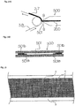
- Figure 2 is a schematic cross-sectional view for describing an exemplary embodiment of lithium ion secondary battery 100 according to the present invention, and schematically illustrates only a part of an electrode stack in an enlarged manner. Here, a part around an end portion on the positive electrode tab side of positive-electrode active material 2 is illustrated.
- Figure 3 illustrates an electrode stack including positive electrodes 1.
- positive-electrode active material 2 is formed on each of opposite surfaces of each positive-electrode current collector 3, and although not illustrated in Figures 1A and 1B , insulating material 40 is provided to straddle a coated portion to which positive-electrode active material 2 has been applied and an uncoated portion (positive electrode tab) to which positive-electrode active material 2 has not been applied.
- First positive-electrode active material layer 2A formed on one surface (upper surface in Figure 2 ) of each positive-electrode current collector 3 includes flat part 2A 1 , inclined part 2A 2 and thin-layer part 2A 3 .
- Thin-layer part 2A 3 is a part positioned on the end portion side (positive electrode tab side) relative to the flat part 2A 1 , the part having a thickness that is smaller than that of flat part 2A 1 .
- Inclined part 2A 2 is a part whose thickness continuously decreases so as to smoothly connect thick flat part 2A 1 and thin-layer part 2A 3 .
- a stepped part whose thickness intermittently decreases may be provided instead of inclined part 2A 2 .
- second positive-electrode active material layer 2B formed on another surface (lower surface in Figure 2 ) of each positive-electrode current collector 3 includes only a flat part.
- One end portion 40a of insulating material 40 is positioned on thin-layer part 2A 3 of first positive-electrode active material layer 2A, and another end portion 40b is positioned on the uncoated portion, that is, the part of positive-electrode current collector 3 on which positive-electrode active material 2 is not formed (positive electrode tab).
- negative-electrode active material 7 is applied to each of a front surface and a back surface of each negative-electrode current collector 8; however, negative-electrode active material 7 includes only a flat part, and includes neither an inclined part nor a thin-layer part.
- the difference in thickness between flat part 2A 1 and thin-layer part 2A 3 of first positive-electrode active material 2A is preferably larger than the thickness of insulating material 40.
- end portion 40a of insulating material 40 positioned on second positive-electrode active material layer 2B is preferably positioned so as to face thin-layer part 2A 3 of first positive-electrode active material layer 2A. Such disposition enables preventing or reducing an increase in thickness caused by insulating materials 40 positioned on the opposite surfaces of each positive-electrode current collector 3.
- each first positive-electrode active material layer 2A (coated portion) enables preventing or reducing an increase in thickness in the part of the electrode stack in which insulating materials 40 are positioned, thereby preventing characteristics of the battery from being affected by the thickness increase.
- the difference in thickness between thin-layer part 2A 3 and flat part 2A 1 of each first positive-electrode active material layer 2A is no less than twice the thickness of one insulating material 40, such a degree of difference is effective because an increase in thickness caused by two insulating materials 40 can be absorbed by the thickness reduction provided by thin-layer part 2A 3 of first positive-electrode active material layer 2A.
- positive-electrode active material layers 2A and 2B on opposite surface of positive-electrode current collector 3 have the same thickness, and thus, even where the thickness of one positive-electrode active material layer (second positive-electrode active material layer 2B) is less than twice the thickness of insulating material 40, as illustrated in Figure 4 , if only flat part 2A 1 of another positive-electrode active material layer (first positive-electrode active material layer 2A) is made thicker in order that a difference in thickness between flat part 2A 1 and thin-layer part 2A 3 may be no less than twice the thickness of insulating material 40, the thickness increase that is caused by two insulating materials 40 can be absorbed by reduction in the thickness provided by thin-layer part 2A 3 , and thus a sufficient effect can be provided.
- each negative electrode 6 on the side that is the same as the end portion of each first positive-electrode active material layer 2A in which inclined part 2A 2 and thin-layer part 2A 3 are provided as described above negative-electrode current collector 8 and flat negative-electrode active materials 7 formed on opposite surfaces thereof are cut and terminated.
- each negative-electrode active material 7 on the side that is the same as the side of each first positive-electrode active material layer 2A in which inclined part 2A 2 and thin-layer part 2A 3 are provided neither an inclined part, nor a stepped part nor a thin-layer part is provided.
- the end portion is located at a position facing relevant insulating material 40 across relevant separator 20.
- each of positive-electrode active materials 2 and negative-electrode active materials 7 may include e.g., an unavoidable inclination, irregularities or roundness of respective layers due to, for example, manufacturing variations and/or layer formation capability.
- Each first positive-electrode active material layer 2A may include a stepped part whose thickness decreases in a stepwise fashion, instead of inclined part 2A 2 whose thickness gently decreases as illustrated in Figure 3 .
- each first positive-electrode active material layer 2A may include both inclined part 2A 2 and the stepped part.
- thin-layer part 2A 3 is not provided independently from inclined part 2A 2 and the stepped part; and a part of inclined part 2A 2 or the stepped part which has a decreased thickness, faces relevant insulating material 40, whereby the thickness increase caused by insulating material 40 is absorbed.
- the part of the inclined part 2A 2 or the stepped part which faces insulating material 40 can be regarded as acting as thin-layer part 2A 3 .
- Inclined parts 2A 2 and thin-layer parts 2A 3 illustrated in Figures 2 to 4 and the non-illustrated stepped parts each have a low density compared to flat parts 2A 1 .
- inclined part 2A 2 and thin-layer part 2A 3 are formed only in each first positive-electrode active material layer 2A, rather than an inclined part or a stepped part and a thin-layer part being provided in each of both positive-electrode active material layers 2A and 2B, mainly because the shape of thin-layer part 2A 3 can be formed with good precision and because the electrode capacity loss is small.
- the stepped part and/or the thin-layer part enables preventing or reducing a partial increase in thickness caused by insulating materials.
- a thickness reduction causes a reduction in the amount of active materials, which results in a decrease in battery capacity.
- the inventors' careful studies revealed that provision of thin-layer part 2A 3 in each of positive-electrode active material layers 2A and 2B may make it impossible for thin-layer part 2A 3 to have a sufficiently-small thickness.
- each negative-electrode active material 8 of each negative electrode 6 facing relevant positive electrode 1 across relevant separator 20 has the effect of preventing or reducing a partial thickness increase caused by insulating materials 40; however, in such a case, the amount of negative-electrode active materials 8 decreases, also unfavorably resulting in a battery capacity decrease.
- Figure 5A is a schematic diagram indicating a coating part of a die coater, which is a kind of apparatuses for coating electrodes.
- the die coater applies slurry 200 to a current collector between die head 500 and back roll 400.
- Slurry 200 containing an active material is discharged from discharge port 501 of die head 500 toward the current collector transported on the outer peripheral surface of back roll 400.
- the thickness of slurry 200 on the current collector is controlled by adjusting, e.g., a space between the current collector and discharge port 501, the discharge amount and/or the application speed according to, e.g., a viscosity of slurry 200.
- slurry 200 containing positive-electrode active material 2 is intermittently applied to positive-electrode current collector 3. It should be understood that slurry 200 can continuously be applied to positive-electrode current collector 3.
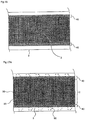
- Figure 5B illustrates a state in which after application of first positive-electrode active material layer 2A to one surface of positive-electrode current collector 3 and after drying of first positive-electrode active material layer 2A, second positive-electrode active material 2B is applied to another surface of positive-electrode current collector 3.
- first positive-electrode active material layer 2A and second positive-electrode active material layer 2B is intermittently formed, and an inclined part and a thin-layer part are formed at each opposite end (an application start end and an application termination end) of each coated portion.
- first positive-electrode active material layer 2A that includes thin-layer part 2A 3 and inclined part 2A 2 are formed on a surface opposite to the surface on which positive-electrode active material layer 2B has been formed.
- the part of positive-electrode current collector 3, to which first positive-electrode active material layer 2A will be subsequently applied is a part on the opposite side of a part in which flat second positive-electrode active material layer 2B comes into close contact with back roll 400 with no gap therebetween. Since no gap is generated between second positive-electrode active material 2B and back roll 400, when first positive-electrode active material 2A is formed on positive-electrode current collector 3, the space between the discharge port 501 and positive-electrode current collector 3 is extremely stable, enabling formation of inclined part 2A 2 and thin-layer part 2A 3 with very good precision.
- the difference in thickness between flat part 2A 1 and thin-layer part 2A 3 of first positive-electrode active material layer 2A can be made to be no less than twice the thickness of insulating material 40 with good precision. Even if the thickness of positive-electrode active material 2 is so small such that a thin-layer part having a thickness decreased by no less than twice the thickness of the insulating material cannot be formed and such that a thickness increase caused by insulating materials 40 cannot completely be absorbed by first positive-electrode active material layer 2A alone, the thickness of first positive-electrode active material 2A can be controlled with good precision, enabling preventing or reducing a partial increase in the thickness of the electrode stack by reducing a thickness of either or both of the negative-electrode active materials to the minimum necessary at respective positions facing the insulating materials.
- provision of a thin-layer part, an inclined part and/or a stepped part in the active material provided on one surface of a current collector effectively prevents or reduces a partial increase in the thickness at a position where insulating materials are provided, and in addition, providing neither a thin-layer part, nor an inclined part, nor a stepped part in the active material provided on another surface of the current collector enables productivity enhancement.
- positive-electrode active material 2 is intermittently applied to each of the opposite surfaces of long band-like positive-electrode current collector 3 for manufacturing a plurality of positive electrodes (positive electrode sheets) 1.
- a surface on the first positive-electrode active material layer 2A side of positive-electrode current collector 3 with positive-electrode active material 2 applied to each of the opposite surfaces thereof is illustrated.
- each first positive-electrode active material layer 2A includes inclined part 2A 2 and thin-layer part 2A 3 in the vicinity of boundary part 4, which serves as a positive electrode tab.
- insulating material 40 is formed so as to cover boundary part 4. As illustrated in Figures 2 and 3 , one end portion 40a of insulating material 40 is positioned on thin-layer part 2A 3 , and another end portion 40b of insulating material 40 is positioned on an uncoated portion. If the thickness of insulating material 40 is too small, a sufficient insulating property cannot be ensured and thus the thickness is preferably no less than 10 ⁇ m.
- insulating material 40 is preferably smaller in thickness than the flat part of positive-electrode active material 2.
- the thickness of insulating material 40 is preferably no more than 90% of the thickness of the flat part of positive-electrode active material 2, more preferably no more than 60% of the thickness of flat part 2b.
- each coated portion positive-electrode active material 2 at boundary part 4 between the coated portion and the relevant uncoated portion may rise substantially perpendicularly to relevant positive-electrode current collector 3 as illustrated in Figures 2 to 4
- the end portion may be slightly inclined as illustrated in Figure 19 .
- the end portion of each coated portion (negative-electrode active material 7) may be slightly inclined or rise substantially perpendicular to relevant negative-electrode current collector 8.
- positive-electrode current collector 3 is cut along each cutting line 90 indicated by a dashed line in Figure 9A to obtain positive electrodes 1 of a desired size, one of which is illustrated in Figure 9B .
- the cutting lines 90 are imaginary lines and thus not actually formed.
- negative-electrode active material 7 is intermittently applied to each of the opposite surfaces of large negative-electrode current collector 8, which is provided for manufacturing a plurality of negative electrodes (negative electrode sheets) 6.
- negative-electrode current collector 8 with negative-electrode active material 7 applied on each of the opposite surfaces thereof is illustrated.
- negative-electrode active material 7 may include a flat part alone in which neither an inclined part, nor a thin-layer part, nor a stepped part are present.
- negative-electrode current collector 8 is divided by cutting negative-electrode current collector 8 along each cutting line 91 indicated by a dashed line in Figure 11A to obtain negative electrodes 6 having a desired size, one of which is illustrated in Figure 11B .
- Cutting lines 91 are imaginary lines and thus are not actually formed.
- Positive electrodes 1 illustrated in Figure 9B and negative electrodes 6 illustrated in Figure 11B formed as described above are alternately stacked via separators 20, and positive electrode terminal 11 and negative electrode terminal 16 are connected to the stacked electrodes, whereby the electrode stack illustrated in Figure 3 is formed.
- the electrode stack is housed and sealed together with electrolyte in an outer container including flexible films 30, whereby secondary battery 100 illustrated in Figures 1A and 1B is formed.
- secondary battery 100 according to the present invention which has been formed as described above, one end portion 40a of each insulating material 40 is positioned on thin-layer part 2A 3 of relevant first positive-electrode active material layer 2A.
- the amount of thickness increase caused by each insulating material 40 formed so as to cover boundary part 4 between the coated portions and the uncoated portion of relevant positive electrode 1 is absorbed (cancelled out) by the thickness reduction provided by thin-layer part 2A 3 and inclined part 2A 2 of relevant first positive-electrode active material layer 2A, preventing or reducing a partial increase in the thickness of the electrode stack, and thus, the electrode stack can be uniformly fastened and held in place, thereby preventing or reducing a deterioration in product quality as regards, for example, variability in the electric characteristics and battery cycle degradation.
- each negative electrode 6 is cut and terminated at a position facing the uncoated portion (positive electrode tab) of relevant positive electrode 1, and as illustrated in Figure 3 , at a position facing the uncoated portion of each positive electrode 1, negative-electrode active material 7 exists on the front and back of negative-electrode current collector 8 with no uncoated portion provided.
- each negative electrode 6 may also be configured in such a manner that an uncoated portion is present at a position in negative electrode 6, the position facing the uncoated portion of positive electrode 1.
- each negative electrode 6 At an end portion of each negative electrode 6, the end portion not facing the uncoated portion of relevant positive electrode 1, an uncoated portion, which serves as a negative electrode tab, is provided. If insulating material (not illustrated) is provided on a boundary part between the coated portion and the uncoated portion of each negative electrode 6, as in the case in which a thickness increase caused by insulating material 40 is cancelled out by means of each positive electrode 1, a thin-layer part, an inclined part and/or a stepped part having a small thickness may be provided in each negative-electrode active material or in each positive-electrode active material, and insulating material may be disposed at a position facing the thin-layer part, the inclined part and/or the stepped part.
- an inclined part 7a can be provided in at least one of negative-electrode active materials 7 in each negative electrode 6 to further reduce the possibility of battery distortion due to insulating materials 40 provided on positive electrodes 1.
- Each insulating material 40 with one end portion 40a positioned on thin-layer part 2A 3 of relevant first positive-electrode active material layer 2A is preferably formed in such a manner that the total thickness of two insulating materials 40 is no larger than the difference in thickness between flat part 2A 1 and thin-layer part 2A 3 of each first positive-electrode active material layer 2A.
- manufacturing variations may prevent the difference in thickness between flat part 2A 1 and thin-layer part 2A 3 of each first positive-electrode active material layer 2A from becoming the desired size.
- each negative-electrode active material 7 enables the thickness increase caused by manufacturing variations of positive electrodes 1 to be absorbed (cancelled out).
- FIG 12 a configuration in which inclined part 7a of each negative-electrode active material 7 is positioned facing insulating material 40 on relevant first positive-electrode active material layer 2A, which includes inclined part 2A 1 and thin-layer part 2A 3 , across relevant separator 20 is illustrated as an example.
- inclined part 7a may be disposed so as to face insulating material 40 on relevant second positive-electrode active material layer 2B, which has neither an inclined part nor a thin-layer part, across relevant separator 20.
- each of thicknesses, distances, etc., of the respective members in the present invention means the average value of values measured at three or more arbitrary positions.
- a mixed active material of LiMn 2 O 4 and LiNi 0.8 Co 0.1 Al 0.1 O 2 was used as positive-electrode active material
- carbon black was used as a conductive agent
- PVdF was used as binder
- slurry 200 in which a compound agent consisting of these materials is dispersed in an organic solvent was prepared.
- This slurry 200 was intermittently applied to positive-electrode current collector 3 having a thickness of 20 ⁇ m and mainly consisting of aluminum and then dried, whereby second positive-electrode active material layers 2B having a thickness of 80 ⁇ m was formed.
- positive-electrode active material 2 coated portions coated with positive-electrode active material 2 and uncoated portions not coated with positive-electrode active material 2 are alternately present along a longitudinal direction of positive-electrode current collector 2.
- positive-electrode active material 2 was intermittently applied to the surface of positive-electrode current collector 3 on the side that is opposite to the side on which second positive-electrode active material layers 2B was formed, and then dried, whereby first positive-electrode active material layers 2A were formed.
- Each first positive-electrode active material layer 2A was configured so as to include flat part 2A 1 having a thickness of 80 ⁇ m, thin-layer part 2A 3 having a thickness 20 ⁇ m and inclined part 2A 2 whose thickness continuously decreases between flat part 2A 1 and thin-layer part 2A 3 .
- a method of applying an active material to a current collector will be described.
- any device that utilizes various coating methods including transfer methods or vapor deposition methods, such as doctor blades, die coaters and gravure coaters, may be used.
- a die coater such as illustrated in Figure 6 .
- Methods of coating active material that use a die coater are generally classified into two methods: a continuous application method in which active material is continuously formed in the longitudinal direction of a long current collector, and an intermittent coating method in which coated portions coated with active material and uncoated portions not coated with the active material are alternately formed along a longitudinal direction of a current collector.
- FIG. 13 is a diagram illustrating an example of a configuration of a die coater that intermittently applies active material.
- a slurry flow path of a die coater that performs intermittent coating includes die head 500, coating valve 502 connected to die head 500, pump 503, and tank 504 that stores slurry 200.
- return valve 505 is provided between tank 504 and coating valve 502.
- a motor valve can vary an open/closed state of the valve with good precision even while slurry 200 is being applied.
- the flow path of slurry 200 is controlled by coating valve 502, which includes a motor valve, in combination with the operation of return valve 505, enabling a coated portion (flat part 2A 1 , inclined part 2A 2 or a stepped part and thin-layer part 2A 3 ) of each active material, an uncoated portion and a boundary part therebetween to be formed into respective desired shapes.
- coating valve 502 includes a motor valve, in combination with the operation of return valve 505, enabling a coated portion (flat part 2A 1 , inclined part 2A 2 or a stepped part and thin-layer part 2A 3 ) of each active material, an uncoated portion and a boundary part therebetween to be formed into respective desired shapes.
- active material can be formed by being continuously applied using the die coater schematically illustrated in Figures 14A and 14B .
- shim 501b including a tapered part or stepped part 501a whose thickness decreases toward the center portion of discharge port 501 is provided. Shims 501b enable formation of active material in such a manner that a stepped part or an inclined part and a thin-layer part are formed at an end portion of each coated portion.
- polypropylene insulating tape (insulating materials) 40 having a thickness of 30 ⁇ m was attached to boundary part 4 between the coated portion and the uncoated portion of each positive electrode 1.
- insulating tape 40 provided so as to cover boundary part 4 on one surface of each positive-electrode active material 2, was formed so that end portion 40a is positioned on thin-layer part 2A 3 of relevant first positive-electrode active material layer 2A.
- Insulating tape 40 provided so as to cover boundary part 4 on another surface of each positive-electrode active material 2, was disposed so that one end portion 40a faces thin-layer part 2A 3 of relevant first positive-electrode active material layer 2A across positive-electrode current collector 3. Then, as illustrated in Figures 9A and 9B , positive-electrode current collector 3 was cut along each cutting line 90 to obtain individual positive electrodes 1.
- Graphite with a surface coated with an amorphous material was used as negative-electrode active material 7 and PVdF was used as a binder, and a slurry in which a compound agent of these materials is dispersed in an organic solvent was prepared. As illustrated in Figure 10 , the slurry was intermittently applied to a copper foil having a thickness of 15 ⁇ m, which is negative-electrode current collector 8, and then dried to fabricate a negative electrode roll including coated portions coated with negative-electrode active material 7 and uncoated portions not coated with negative-electrode active material 7 as with positive electrodes 1. Each negative-electrode active material 7 includes only a flat part having a thickness of 55 ⁇ m.
- a specific method for applying negative-electrode active material 7 is similar to the aforementioned method for applying positive-electrode active material 2, and active material may be intermittently applied using the die coater illustrated in Figure 13 or may be continuously applied using the die coater illustrated in Figures 14A and 14B . Then, as illustrated in Figures 11A and 11B , negative-electrode current collector 8 was cut along each cutting line 91 to obtain individual negative electrodes 6.
- Each negative electrode 6 includes a negative electrode tab, which is an uncoated portion not coated by negative-electrode active material 7, at a position that does not face a positive electrode tab, and negative-electrode current collector 8 was cut at a part that faces a positive electrode tab and that has negative-electrode active materials 7 on both surfaces thereof. Insulating material is not provided at a boundary part between the coated portion and the uncoated portion of each negative electrode 6.
- Obtained positive electrodes 1 and negative electrodes 6 were alternately stacked via separators 20 having a thickness of 25 ⁇ m, each separator 20 made of polypropylene, and negative electrode terminal 16 and positive electrode terminal 11 were attached to the stack, which was then housed in an outer container consisting of flexible films 30, whereby a stacked type secondary battery having a thickness of 8 mm was obtained.
- Each first positive-electrode active material layer 2A includes a flat part 2A 1 having a thickness of 35 ⁇ m, a thin-layer part 2A 3 having a thickness of 5 ⁇ m, and an inclined part 2A 2 whose thickness continuously decreases between flat part 2A 1 and thin-layer part 2A 3 .
- Each second positive-electrode active material layer 2B includes only a flat part having a thickness of 35 ⁇ m.
- polypropylene insulating tapes (insulating materials) 40 having a thickness of 30 ⁇ m were attached and then positive-electrode current collector 3 was cut to obtain individual positive electrodes 1.
- Negative-electrode active materials 7 according to the present example were configured so as to each include a flat part having a thickness of 35 ⁇ m, a thin-layer part having a thickness of 5 ⁇ m and an inclined part whose thickness continuously decreases from the flat part to the thin-layer part.
- each negative electrode 6 was disposed so as to face inclined part 2A 2 and thin-layer part 2A 3 of relevant first positive-electrode active material layer 2A via a relevant separator.
- the rest of the conditions was made to be similar to those of example 1, and a stacked type secondary battery having a thickness of 3 mm was obtained.
- a positive-electrode active material on each of the opposite surfaces of positive-electrode current collector 3 was formed as a layer having a uniform thickness, the layer having neither a thin-layer part, nor an inclined part, nor a stepped part, and was configured so as to include only a flat part with no inclined part provided.
- the rest of the conditions was made to be similar to those of example 1, and a stacked type secondary battery was obtained.
- the thickness of the stacked type battery was approximately 8 mm at the center portion and approximately 9 mm around an end portion.
- the stacked type batteries according to examples 1 and 2 provide a very stable discharge capacity and cycle characteristics, and that the discharge capacity and cycle characteristics of the battery according to the comparative example are unstable compared to those of the batteries according to examples 1 and 2.
- the stable battery characteristics can be considered as resulting from preventing or reducing an increase in the thickness of a part of the stacked type battery in which insulating materials 40 are positioned from being increased so as to be larger than a thickness of the rest of the parts and thus enabling the stacked type battery to be held in place while uniform pressure is applied to it.
- positive-electrode active materials 2 and negative-electrode active materials 7 are formed by being intermittently applied; however, as illustrated in Figures 15 to 17B , positive-electrode active materials 2 and negative-electrode active materials 7 may be formed by being continuously applied so as to form active material layer with no intervals over a plurality of electrode forming parts.
- active materials are formed by means of being continuously applied, before the electrodes are cut out along each cutting line 90 in Figure 17A , they can be kept in the form of an electrode roll as illustrated in Figure 18 , and in such a case, extreme distortion of parts in which insulating materials 40 are disposed can be prevented, thereby enhancing the product quality of the electrodes.
- the present invention is useful for manufacturing electrodes for a lithium ion secondary battery and manufacturing a lithium ion secondary battery using such electrodes, and is also effectively employed for a secondary battery other than a lithium ion battery.
Landscapes
- Chemical & Material Sciences (AREA)
- Engineering & Computer Science (AREA)
- Chemical Kinetics & Catalysis (AREA)
- Electrochemistry (AREA)
- General Chemical & Material Sciences (AREA)
- Manufacturing & Machinery (AREA)
- Materials Engineering (AREA)
- Secondary Cells (AREA)
- Battery Electrode And Active Subsutance (AREA)
- Connection Of Batteries Or Terminals (AREA)
Description
- The present invention relates to a secondary battery including a positive electrode and a negative electrode laid over each other with a separator interposed therebetween, and a method for manufacturing the same.
- Secondary batteries are becoming widely used as power supplies for vehicles and household appliances, and not only as power supplies for portable devices such as mobile phones, digital cameras and laptop computers, and among others, lithium ion secondary batteries, which have a high-energy density and are lightweight, are energy storage devices that are indispensable in daily life.
- Secondary batteries are generally classified into a rolled type and a stacked type. A battery electrode assembly of a rolled type secondary battery has a structure in which a long positive electrode sheet and a long negative electrode sheet laid on each other via a separator are rolled a plurality of turns. A battery electrode assembly of a stacked type secondary battery has a structure in which positive electrode sheets and negative electrode sheets are alternately stacked with separators interposed therebetween. The positive electrode sheets and the negative electrode sheets each include a current collector including a coated portion to which active material (which may be a compound agent containing, e.g., a binder and a conductive material) has been applied and an uncoated portion to which active material has not been applied in order to allow an electrode terminal to be connected thereto.
- In either a rolled type secondary battery or a stacked type secondary battery, a battery electrode assembly is enclosed inside an outer container in such a manner that: one end of a positive electrode terminal is electrically connected to an uncoated portion of a positive electrode sheet and another end of the positive electrode terminal extends to the outside of the outer container (outer case); and one end of a negative electrode terminal is electrically connected to an uncoated portion of a negative electrode sheet and another end of the negative electrode terminal extends to the outside of the outer container. Inside the outer container, in addition to the battery electrode assembly, electrolyte is enclosed. Capacities of secondary batteries have been increasing year by year, and along with this increase, heat that would be generated if a shortcut occurs also increases, causing an increase in risk, and thus, measures to ensure battery safety are becoming increasingly important.
- As an example of a safety countermeasure, a technique in which insulating material is formed on a boundary part between a coated portion and an uncoated portion in order to prevent a shortcut between a positive electrode and a negative electrode is known (Patent Document 1).
- Patent Document 1:
JP2012-164470A -
EP 2 966 721 A1 relates to a non-aqueous electrolyte secondary battery including a negative electrode in which a negative electrode active material layer is formed on a negative electrolyte collector and a positive electrode laminated on the negative electrode through a separator. -
EP 3 012 898 A1 -
US 2009/024661 A1 relates to an electrochemical device having an electrode matrix including a multilayer structure laminating positive and negative electrodes with a separator interposed there between. -
US 2006/008702 A1 relates to a secondary battery including an electrode assembly with a positive electrode, a negative electrode and a separator disposed between the positive and the negative electrodes. -
JP H09 180704 A -
JP 2004 303622 A -
US 2006/0006063 A1 relates to a method of manufacturing an electrode and the electrode. -
JP 2006 147392 A - The present invention is defined by the independent claims. Dependent claims refer to preferred embodiments.
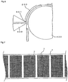
- In the technique disclosed in
Patent Document 1, as illustrated inFigure 19 ,positive electrode 1 andnegative electrode 6 are alternately stacked viaseparator 20, and oncurrent collector 3 of eachpositive electrode 1,insulating material 40 coveringboundary part 4 between a coated portion to whichactive material 2 has been applied and an uncoated portion to whichactive material 2 has not been applied is formed. In a stacked type secondary battery, insulatingmaterials 40 are stacked at the same position in a planar view. Thus, the thickness of a part of the battery electrode assembly at the position whereinsulating materials 40 are disposed, becomes thicker, which results in reducing energy density per unit volume. - Also, in order to obtain stable electric characteristics and high reliability, it is preferable that the battery electrode assembly of a secondary battery be fastened via, e.g., a tape by applying pressure uniformly. However, use of insulating materials in a stacked type secondary battery in such a manner as in
Patent Document 1 results in failure to uniformly fasten a battery electrode assembly due to a difference in thickness between a part in whichinsulating materials 40 are present and a part in which insulatingmaterials 40 are not present, which may cause battery quality deterioration such as variability in electric characteristics and/or degradation of battery cycle properties. - Therefore, an object of the present invention is to solve the aforementioned problems and provide a high-quality secondary battery having high electric characteristics and high reliability, the secondary battery preventing a short circuit between a positive electrode and a negative electrode by means of insulating material and preventing or reducing an increase in volume and deformation of a battery electrode assembly, and a method for manufacturing the same.
- The invention is defined by the independent claims. Dependent claims refer to preferred embodiments.
- A secondary battery according to the present invention comprises a battery electrode assembly including a positive electrode and a negative electrode alternately stacked via a separator, and the positive electrode and the negative electrode each includes a current collector and active material applied to the current collector. The active material positioned on one surface of the current collector of the positive electrode, includes a flat part and a small-thickness part positioned on an end portion side relative to the flat part, the small-thickness part having a thickness that is smaller than that of the flat part. The active material positioned on another surface of the current collector of the positive electrode, which faces the small-thickness part of the active material positioned on the one surface, across the current collector, is a flat part having a constant thickness.
- The present invention enables preventing or reducing an increase in volume of a battery electrode assembly and distortion of the battery electrode assembly that are caused by insulating material, and enables provision of a high-quality secondary battery having good energy density.
-
- [
Figure 1A] Figure 1A is a plan view illustrating a basic structure of a stacked type secondary battery according to the present invention. - [
Figure 1B] Figure 1B is a cross-sectional view along line A-A inFigure 1A . - [
Figure 2] Figure 2 is an enlarged cross-sectional view illustrating a positive electrode in an exemplary embodiment of a secondary battery of the present invention. - [
Figure 3] Figure 3 is an enlarged cross-sectional view illustrating a major part of an exemplary embodiment of a secondary battery according to the present invention. - [
Figure 4] Figure 4 is an enlarged cross-sectional view illustrating a variation of a positive electrode in an exemplary embodiment of a secondary battery of the present invention. - [
Figure 5A] Figure 5A is a schematic diagram illustrating an example of an electrode coating apparatus. - [
Figure 5B] Figure 5B is a schematic diagram illustrating a reference example of an electrode manufacturing method. - [
Figure 6] Figure 6 is a schematic diagram illustrating an example of an electrode manufacturing method according to the present invention. - [
Figure 7] Figure 7 is a plan view illustrating a positive electrode forming step in a secondary battery manufacturing method according to the present invention. - [
Figure 8] Figure 8 is a plan view illustrating a step followingFigure 7 in the secondary battery manufacturing method according to the present invention. - [
Figure 9A] Figure 9A is a plan view illustrating a step followingFigure 8 in the secondary battery manufacturing method according to the present invention. - [
Figure 9B] Figure 9B is a plan view illustrating a positive electrode formed as a result of cutting in the step illustrated inFigure 9A . - [
Figure 10] Figure 10 is a plan view illustrating a negative electrode forming step in the secondary battery manufacturing method according to the present invention. - [
Figure 11A] Figure 11A is a plan view illustrating a step followingFigure 10 in the secondary battery manufacturing method according to the present invention. - [
Figure 11B] Figure 11B is a plan view illustrating a negative electrode formed as a result of cutting in the step illustrated inFigure 11A . - [
Figure 12] Figure 12 is an enlarged cross-sectional view illustrating a major part of another exemplary embodiment of a secondary battery according to the present invention. - [
Figure 13] Figure 13 is a block diagram schematically illustrating an example of an apparatus used for intermittent application of active material. - [
Figure 14A] Figure 14A is a cross-sectional view schematically illustrating an example of an apparatus used for continuous application of active material. - [
Figure 14B] Figure 14B is an enlarged cross-sectional view along line B-B inFigure 14B . - [
Figure 15] Figure 15 is a plan view illustrating another example of a positive electrode forming step in a secondary battery manufacturing method according to the present invention. - [
Figure 16] Figure 16 is a plan view illustrating a step followingFigure 15 in the secondary battery manufacturing method according to the present invention. - [
Figure 17A] Figure 17A is a plan view illustrating a step followingFigure 16 in the secondary battery manufacturing method according to the present invention. - [
Figure 17B] Figure 17B is a plan view illustrating a positive electrode formed as a result of cutting in the step illustrated inFigure 17A . - [
Figure 18] Figure 18 is a perspective diagram illustrating an electrode roll used in the secondary battery manufacturing method illustrated inFigures 15 to 17B . - [
Figure 19] Figure 19 is an enlarged view illustrating a major part of a stacked type secondary battery according to a related art. - An exemplary embodiment of the present invention will be described below with reference to the drawings.
-
Figure 1 schematically illustrates an example of a configuration of a stacked type lithium ion secondary battery employing the present invention.Figure 1A is a plan view as viewed from the upper side perpendicular to a principal surface (planar surface) of the secondary battery, andFigure 1B is a cross-sectional view along line A-A inFigure 1A . - Lithium ion
secondary battery 100 according to the present invention includes an electrode stack (battery electrode assembly) formed by alternately stacking positive electrodes (positive electrode sheets) 1 and negative electrodes (negative electrode sheets) 6 viaseparators 20. The electrode stack is housed together with an electrolyte in an outer container consisting offlexible films 30. One end ofpositive electrode terminal 11 is connected topositive electrodes 1 of the electrode stack, and one end ofnegative electrode terminal 16 is connected tonegative electrodes 6, and another end side ofpositive electrode terminal 11 and another end side ofnegative electrode terminal 16 extend to the outside of theflexible films 30. InFigure 1B , illustration of a part of the layers (layers positioned in the intermediate part in a thickness direction) included in the electrode stack is omitted but the electrolyte is illustrated. - Each
positive electrode 1 includes positive-electrodecurrent collector 3 and positive-electrodeactive materials 2 applied to positive-electrodecurrent collector 3, and on each of a front surface and a back surface of positive-electrodecurrent collector 3, a coated portion to which positive-electrodeactive material 2 has been applied and an uncoated portion to which positive-electrodeactive material 2 has not been applied are positioned side by side along a longitudinal direction. Likewise, eachnegative electrode 6 includes negative-electrodecurrent collector 8 and negative-electrodeactive materials 7 applied to negative-electrodecurrent collector 8, and on each of a front surface and a back surface of negative-electrodecurrent collector 8, a coated portion and an uncoated portion are positioned side by side along the longitudinal direction. A planar position ofboundary part 4 between the coated portion and the uncoated portion of eachpositive electrode 1 and a planar position ofboundary part 4 between the coated portion and the uncoated portion of eachnegative electrode 6 may be the same or different (not aligned in planar view) between the front surface and the back surface of the relevant current collector. - The uncoated portion of each of
positive electrodes 1 andnegative electrodes 6 is used as a tab for connection with an electrode terminal (positive electrode terminal 11 or negative electrode terminal 16). The positive electrode tabs connected to respectivepositive electrodes 1 are bundled onpositive electrode terminal 11 and are mutually connected together withpositive electrode terminal 11 by means of, e.g. ultrasonic welding. The negative electrode tabs connected to respectivenegative electrodes 6 are bundled onnegative electrode terminal 16 and are mutually connected together withnegative electrode terminal 16 by means of, e.g., ultrasonic welding. On that basis, the other end portion ofpositive electrode terminal 11 and the other end portion ofnegative electrode terminal 16 extend to the outside of the outer container. - As illustrated in
Figure 2 , insulatingmaterial 40 for preventing the occurrence of a short circuit innegative electrode terminal 16 is formed so as to coverboundary part 4 between the coated portion and the uncoated portion of eachpositive electrode 1. Insulatingmaterial 40 is formed to straddle both the positive electrode tab and positive-electrodeactive material 2 so as to coverboundary part 4. Formation of insulatingmaterial 40 will be described later. - Outer dimensions of the coated portion (negative-electrode active material 7) of each
negative electrode 6 are larger than those of the coated portion (positive-electrode active material 2) of eachpositive electrode 1 and are smaller than or equal to those of eachseparator 20. - In the battery illustrated in
Figures 1A and 1B , examples of positive-electrodeactive material 2 include layered oxide materials such as LiCoO2, LiNiO2, LiNi(1-x)CoO2, LiNix(CoAl)(1-x)O2, Li2MO3-LiMO2, LiNi1/3Co1/3Mn1/3O2, spinel materials such as LiMn2O4, LiMn1.5Ni0.5O4, LiMn(2-x)MxO4, olivine materials such as LiMPO4, olivine fluoride materials such as Li2MPO4F and Li2MSiO4F, and vanadium oxide materials such as V2O5. One of the above materials or a mixture of two or more selected from among the above materials may be used as positive-electrodeactive material 2. - As negative-electrode
active material 7, carbon materials such as graphite, amorphous carbon, diamond-like carbon, fullerene, carbon nanotube, carbon nanohorn, lithium metal materials, silicon- or tin-based alloy materials, oxide-based materials such as Nb2O5 and TiO2, or a composite of them may be used. - A binding agent and/or a conductive assistant may arbitrarily be added to positive-electrode
active material 2 and negative-electrodeactive material 7. As the conductive assistant, carbon black or carbon fiber or graphite or the like can be used and the combination of two or more of the above materials can be used. As the binding agent, polyvinylidene fluoride, polytetrafluoroethylene, carboxymethyl cellulose, modified acrylonitrile rubber particles or the like may be used. - As positive-electrode
current collector 3, aluminum, stainless steel, nickel, titanium or an alloy containing any of these materials can be used, and in particular, aluminum is preferable. As negative-electrodecurrent collector 8, copper, stainless steel, nickel, titanium or an alloy containing any of these materials can be used. - As the electrolyte, one organic solvent selected from among cyclic carbonates such as ethylene carbonate, propylene carbonate, vinylene carbonate and butylene carbonate, chain carbonates such as ethyl methyl carbonate (EMC), diethyl carbonate (DEC), dimethyl carbonate (DMC) and dipropyl carbonate (DPC), aliphatic carboxylic acid esters, γ-lactones such as γ-butyrolactone, chain ethers, and cyclic ethers may be used and the mixture of two or more of the above materials may be used. Furthermore, a lithium salt can be dissolved in the organic solvent(s).
-
Separator 20 is formed mainly of a porous membrane, woven fabric, nonwoven fabric that are made of resin. As the resin component inseparator 20, polyolefin-based resin such as polypropylene or polyethylene, polyester resin, acrylic resin, styrene resin, nylon resin or the like can be used, for example. A polyolefin-based microporous membrane is particularly preferable because the polyolefin-based microporous membrane has excellent ion-permeating properties and excellent performance characteristics for physically separating a positive electrode and a negative electrode. A layer containing inorganic particles may be formed inseparator 20 as needed. Examples of the inorganic particles include insulating oxide, silicate, nitride, and carbide. In particular, the inorganic particles preferably contain TiO2 or Al2O3. - As the outer container, a case made of
flexible film 30 or a can case can be used. From the point of view of battery weight reduction, usingflexible film 30 is preferable. Asflexible film 30, a film in which resin layers are provided on both the front and rear surfaces of a metal layer as a base material can be used. As the metal layer, a layer having barrier properties which may be properties for preventing leakage of an electrolyte and infiltration of moisture from the outside can be selected, and aluminum, stainless steel or the like can be used. A thermally-fusible resin layer such as modified polyolefin is provided on at least one surface of the metal layer. The thermally-fusible resin layers offlexible film 30 are opposite to each other and are thermally fused to each other in the part that surrounds the space where the laminated electrode assembly is stored, thereby the outer container is formed. A resin layer such as a nylon film and a polyester film may be provided on the surface of the outer container opposite to the surface on which the thermally-fusible resin layer is formed. - As
positive electrode terminal 11, a terminal formed of aluminum or aluminum alloy can be used. Asnegative electrode terminal 16, a terminal formed of copper, copper alloy, or nickel-plated copper or copper alloy can be used. Each of the other ends ofterminals terminals - Insulating
material 40 that is formed to cover boundary part 4a between a coated portion and an uncoated portion of positive electrodeactive material 2 can be made of polyimide, glass fiber, polyester, polypropylene, or a material including these. Insulatingmaterial 40 may be formed by applying heat to a tape-like resin member to weld the resin member to boundary part 4a or by applying a gel resin to boundary part 4a and drying the resin. -
Figure 2 is a schematic cross-sectional view for describing an exemplary embodiment of lithium ionsecondary battery 100 according to the present invention, and schematically illustrates only a part of an electrode stack in an enlarged manner. Here, a part around an end portion on the positive electrode tab side of positive-electrodeactive material 2 is illustrated.Figure 3 illustrates an electrode stack includingpositive electrodes 1. - As illustrated in
Figures 2 and 3 , positive-electrodeactive material 2 is formed on each of opposite surfaces of each positive-electrodecurrent collector 3, and although not illustrated inFigures 1A and 1B , insulatingmaterial 40 is provided to straddle a coated portion to which positive-electrodeactive material 2 has been applied and an uncoated portion (positive electrode tab) to which positive-electrodeactive material 2 has not been applied. First positive-electrodeactive material layer 2A formed on one surface (upper surface inFigure 2 ) of each positive-electrodecurrent collector 3 includesflat part 2A1,inclined part 2A2 and thin-layer part 2A3. Thin-layer part 2A3 is a part positioned on the end portion side (positive electrode tab side) relative to theflat part 2A1, the part having a thickness that is smaller than that offlat part 2A1.Inclined part 2A2 is a part whose thickness continuously decreases so as to smoothly connect thickflat part 2A1 and thin-layer part 2A3. However, instead ofinclined part 2A2, a stepped part whose thickness intermittently decreases may be provided. On the other hand, second positive-electrodeactive material layer 2B formed on another surface (lower surface inFigure 2 ) of each positive-electrodecurrent collector 3 includes only a flat part. Oneend portion 40a of insulatingmaterial 40 is positioned on thin-layer part 2A3 of first positive-electrodeactive material layer 2A, and anotherend portion 40b is positioned on the uncoated portion, that is, the part of positive-electrodecurrent collector 3 on which positive-electrodeactive material 2 is not formed (positive electrode tab). As illustrated inFigure 3 , in eachnegative electrode 6, also, negative-electrodeactive material 7 is applied to each of a front surface and a back surface of each negative-electrodecurrent collector 8; however, negative-electrodeactive material 7 includes only a flat part, and includes neither an inclined part nor a thin-layer part. - The difference in thickness between
flat part 2A1 and thin-layer part 2A3 of first positive-electrodeactive material 2A is preferably larger than the thickness of insulatingmaterial 40. Also,end portion 40a of insulatingmaterial 40 positioned on second positive-electrodeactive material layer 2B is preferably positioned so as to face thin-layer part 2A3 of first positive-electrodeactive material layer 2A. Such disposition enables preventing or reducing an increase in thickness caused by insulatingmaterials 40 positioned on the opposite surfaces of each positive-electrodecurrent collector 3. In other words, adjustment (reduction) of the thickness of an outer edge portion of each first positive-electrodeactive material layer 2A (coated portion) enables preventing or reducing an increase in thickness in the part of the electrode stack in which insulatingmaterials 40 are positioned, thereby preventing characteristics of the battery from being affected by the thickness increase. In particular, if the difference in thickness between thin-layer part 2A3 andflat part 2A1 of each first positive-electrodeactive material layer 2A is no less than twice the thickness of one insulatingmaterial 40, such a degree of difference is effective because an increase in thickness caused by two insulatingmaterials 40 can be absorbed by the thickness reduction provided by thin-layer part 2A3 of first positive-electrodeactive material layer 2A. Here, since it is not necessary that positive-electrodeactive material layers current collector 3 have the same thickness, and thus, even where the thickness of one positive-electrode active material layer (second positive-electrodeactive material layer 2B) is less than twice the thickness of insulatingmaterial 40, as illustrated inFigure 4 , if onlyflat part 2A1 of another positive-electrode active material layer (first positive-electrodeactive material layer 2A) is made thicker in order that a difference in thickness betweenflat part 2A1 and thin-layer part 2A3 may be no less than twice the thickness of insulatingmaterial 40, the thickness increase that is caused by two insulatingmaterials 40 can be absorbed by reduction in the thickness provided by thin-layer part 2A3, and thus a sufficient effect can be provided. - At an end portion of each
negative electrode 6 on the side that is the same as the end portion of each first positive-electrodeactive material layer 2A in which inclinedpart 2A2 and thin-layer part 2A3 are provided as described above, negative-electrodecurrent collector 8 and flat negative-electrodeactive materials 7 formed on opposite surfaces thereof are cut and terminated. In other words, at the end portion of each negative-electrodeactive material 7 on the side that is the same as the side of each first positive-electrodeactive material layer 2A in which inclinedpart 2A2 and thin-layer part 2A3 are provided, neither an inclined part, nor a stepped part nor a thin-layer part is provided. The end portion is located at a position facing relevant insulatingmaterial 40 acrossrelevant separator 20. - In
Figure 3 , for ease of viewing,positive electrodes 1,negative electrode 6 andseparators 20 are illustrated so as not to be in contact with one another; however, in reality,positive electrodes 1,negative electrode 6 andseparators 20 are stacked in close contact with one another. In the configuration illustrated inFigure 3 , as described above, the difference in thickness betweeninclined part 2A1 and thin-layer part 2A3 of each first positive-electrodeactive material layer 2A is more than twice the thickness of each insulatingmaterial 40, and thus, whenpositive electrodes 1,negative electrodes 6 andseparators 20 are brought into close contact with one another,positive electrodes 1 are curved at respective positions of thin-layer parts 2A3, enabling preventing or reducing a partial increase in the thickness of the electrode stack caused by insulatingmaterials 40. As described above,Figure 3 illustrates a configuration in whichpositive electrodes 1 are curved; however, a configuration in which onlynegative electrodes 6 are curved or a configuration in which bothpositive electrodes 1 andnegative electrodes 6 are curved can be employed. - Here, it is not necessary that
flat part 2A1 and thin-layer part 2A3 be disposed in parallel to each other on each positive-electrodecurrent collector 3, and an edge ofboundary part 4 between a coated portion and an uncoated portion of eachpositive electrode 1 and an edge of an end portion of eachnegative electrode 6 may each have a round curve shape, rather than a linear shape perpendicular to a direction in which relevantcurrent collector active materials 2 and negative-electrodeactive materials 7 may include e.g., an unavoidable inclination, irregularities or roundness of respective layers due to, for example, manufacturing variations and/or layer formation capability. - Each first positive-electrode
active material layer 2A may include a stepped part whose thickness decreases in a stepwise fashion, instead ofinclined part 2A2 whose thickness gently decreases as illustrated inFigure 3 . Alternatively, each first positive-electrodeactive material layer 2A may include bothinclined part 2A2 and the stepped part. Also, it is possible that: thin-layer part 2A3 is not provided independently frominclined part 2A2 and the stepped part; and a part ofinclined part 2A2 or the stepped part which has a decreased thickness, faces relevant insulatingmaterial 40, whereby the thickness increase caused by insulatingmaterial 40 is absorbed. In such a case, the part of theinclined part 2A2 or the stepped part which faces insulatingmaterial 40, can be regarded as acting as thin-layer part 2A3.Inclined parts 2A2 and thin-layer parts 2A3 illustrated inFigures 2 to 4 and the non-illustrated stepped parts each have a low density compared toflat parts 2A1. - In the configuration illustrated in
Figure 3 ,inclined part 2A2 and thin-layer part 2A3 are formed only in each first positive-electrodeactive material layer 2A, rather than an inclined part or a stepped part and a thin-layer part being provided in each of both positive-electrodeactive material layers layer part 2A3 can be formed with good precision and because the electrode capacity loss is small. - For example, if an inclined part, a stepped part and/or a thin-layer part are provided in each of both first positive-electrode
active material layers 2A and second positive-electrodeactive materials 2B, and if insulatingmaterial 40 is disposed so as to face the inclined part, the stepped part and/or the thin-layer part enables preventing or reducing a partial increase in thickness caused by insulating materials. However, a thickness reduction causes a reduction in the amount of active materials, which results in a decrease in battery capacity. Also, the inventors' careful studies revealed that provision of thin-layer part 2A3 in each of positive-electrodeactive material layers layer part 2A3 to have a sufficiently-small thickness. In such a case, the electrodes could not be used as products and would be discarded as defective products, which results in deterioration in productivity. Also, provision of a thin-layer part, an inclined part and/or a stepped part in each negative-electrodeactive material 8 of eachnegative electrode 6 facing relevantpositive electrode 1 acrossrelevant separator 20 has the effect of preventing or reducing a partial thickness increase caused by insulatingmaterials 40; however, in such a case, the amount of negative-electrodeactive materials 8 decreases, also unfavorably resulting in a battery capacity decrease. - For a more detailed evaluation, it was found that a failure to form a thin-layer part, an inclined part and/or a stepped part of positive-electrode
active material 2 with good precision and unstable formation of the thin-layer part, the inclined part and/or the stepped part are partly attributable to a tendency of such parts being formed so as to lean toward either first positive-electrodeactive material 2A or second positive-electrodeactive material 2B. This will be described using the reference example illustrated inFigures 5A and 5B . -
Figure 5A is a schematic diagram indicating a coating part of a die coater, which is a kind of apparatuses for coating electrodes. The die coater appliesslurry 200 to a current collector betweendie head 500 andback roll 400.Slurry 200 containing an active material is discharged fromdischarge port 501 ofdie head 500 toward the current collector transported on the outer peripheral surface ofback roll 400. The thickness ofslurry 200 on the current collector is controlled by adjusting, e.g., a space between the current collector and dischargeport 501, the discharge amount and/or the application speed according to, e.g., a viscosity ofslurry 200. In the example illustrated inFigures 5A and 5B ,slurry 200 containing positive-electrodeactive material 2 is intermittently applied to positive-electrodecurrent collector 3. It should be understood thatslurry 200 can continuously be applied to positive-electrodecurrent collector 3. -
Figure 5B illustrates a state in which after application of first positive-electrodeactive material layer 2A to one surface of positive-electrodecurrent collector 3 and after drying of first positive-electrodeactive material layer 2A, second positive-electrodeactive material 2B is applied to another surface of positive-electrodecurrent collector 3. Each of first positive-electrodeactive material layer 2A and second positive-electrodeactive material layer 2B is intermittently formed, and an inclined part and a thin-layer part are formed at each opposite end (an application start end and an application termination end) of each coated portion. Whenslurry 200 is discharged fromdischarge port 501 ofdie head 500 in order to form second positive-electrodeactive material layer 2B on the surface of positive-electrodecurrent collector 3 on the side opposite to a surface on which first positive-electrodeactive material layer 2A has already been formed, a gap is generated between the inclined part and the thin-layer part of each first positive-electrodeactive material 2A andback roll 400.Slurry 200 is pressurized indie head 500, and upon discharge ofslurry 200, positive-electrodecurrent collector 3 is pushed in a direction in which gap h is eliminated, that is, toward theback roll 400 side, whereby the space between thedischarge port 501 and positive-electrodecurrent collector 3 is increased. As described above, it was found that if an active material including an inclined part and a thin-layer part is formed on one surface and then an active material is formed on another surface, the space betweendischarge port 501 and the current collector is not stable and an active material that is subsequently formed tends to have an unstable thickness and inclination. - Therefore, in the present invention, as illustrated in
Figure 6 , after flat second positive-electrodeactive material layer 2B, that does not include a thin-layer part, an inclined part, and a stepped part are formed on positive-electrodecurrent collector 3; first positive-electrodeactive material layer 2A, that includes thin-layer part 2A3 andinclined part 2A2 are formed on a surface opposite to the surface on which positive-electrodeactive material layer 2B has been formed. Then, the part of positive-electrodecurrent collector 3, to which first positive-electrodeactive material layer 2A will be subsequently applied, is a part on the opposite side of a part in which flat second positive-electrodeactive material layer 2B comes into close contact withback roll 400 with no gap therebetween. Since no gap is generated between second positive-electrodeactive material 2B andback roll 400, when first positive-electrodeactive material 2A is formed on positive-electrodecurrent collector 3, the space between thedischarge port 501 and positive-electrodecurrent collector 3 is extremely stable, enabling formation ofinclined part 2A2 and thin-layer part 2A3 with very good precision. Therefore, the difference in thickness betweenflat part 2A1 and thin-layer part 2A3 of first positive-electrodeactive material layer 2A can be made to be no less than twice the thickness of insulatingmaterial 40 with good precision. Even if the thickness of positive-electrodeactive material 2 is so small such that a thin-layer part having a thickness decreased by no less than twice the thickness of the insulating material cannot be formed and such that a thickness increase caused by insulatingmaterials 40 cannot completely be absorbed by first positive-electrodeactive material layer 2A alone, the thickness of first positive-electrodeactive material 2A can be controlled with good precision, enabling preventing or reducing a partial increase in the thickness of the electrode stack by reducing a thickness of either or both of the negative-electrode active materials to the minimum necessary at respective positions facing the insulating materials. - As described above, provision of a thin-layer part, an inclined part and/or a stepped part in the active material provided on one surface of a current collector effectively prevents or reduces a partial increase in the thickness at a position where insulating materials are provided, and in addition, providing neither a thin-layer part, nor an inclined part, nor a stepped part in the active material provided on another surface of the current collector enables productivity enhancement.
- First, as described above, in the step illustrated in
Figure 6 , positive-electrodeactive material 2 is intermittently applied to each of the opposite surfaces of long band-like positive-electrodecurrent collector 3 for manufacturing a plurality of positive electrodes (positive electrode sheets) 1. InFigure 7 , a surface on the first positive-electrodeactive material layer 2A side of positive-electrodecurrent collector 3 with positive-electrodeactive material 2 applied to each of the opposite surfaces thereof is illustrated. Although not clearly illustrated inFigure 7 , each first positive-electrodeactive material layer 2A includesinclined part 2A2 and thin-layer part 2A3 in the vicinity ofboundary part 4, which serves as a positive electrode tab. Then, as illustrated inFigure 8 , insulatingmaterial 40 is formed so as to coverboundary part 4. As illustrated inFigures 2 and 3 , oneend portion 40a of insulatingmaterial 40 is positioned on thin-layer part 2A3, and anotherend portion 40b of insulatingmaterial 40 is positioned on an uncoated portion. If the thickness of insulatingmaterial 40 is too small, a sufficient insulating property cannot be ensured and thus the thickness is preferably no less than 10 µm. Also, if the thickness of the insulatingmaterial 40 is excessively large, the effect of preventing or reducing an increase in the thickness of the electrode stack, which is provided by the present invention, cannot be sufficiently realized, and thus, insulatingmaterial 40 is preferably smaller in thickness than the flat part of positive-electrodeactive material 2. The thickness of insulatingmaterial 40 is preferably no more than 90% of the thickness of the flat part of positive-electrodeactive material 2, more preferably no more than 60% of the thickness of flat part 2b. Although the end portion of each coated portion (positive-electrode active material 2) atboundary part 4 between the coated portion and the relevant uncoated portion may rise substantially perpendicularly to relevant positive-electrodecurrent collector 3 as illustrated inFigures 2 to 4 , the end portion may be slightly inclined as illustrated inFigure 19 . Also, in eachnegative electrode 6, the end portion of each coated portion (negative-electrode active material 7) may be slightly inclined or rise substantially perpendicular to relevant negative-electrodecurrent collector 8. - Subsequently, in order to obtain
positive electrodes 1 used for individual stacked type batteries, positive-electrodecurrent collector 3 is cut along each cuttingline 90 indicated by a dashed line inFigure 9A to obtainpositive electrodes 1 of a desired size, one of which is illustrated inFigure 9B . The cutting lines 90 are imaginary lines and thus not actually formed. - Meanwhile, with a method that is similar to the step illustrated in
Figure 6 , negative-electrodeactive material 7 is intermittently applied to each of the opposite surfaces of large negative-electrodecurrent collector 8, which is provided for manufacturing a plurality of negative electrodes (negative electrode sheets) 6. InFigure 10 , negative-electrodecurrent collector 8 with negative-electrodeactive material 7 applied on each of the opposite surfaces thereof is illustrated. If the difference in thickness betweenflat part 2A1 and thin-layer part 2A3 of each first positive-electrodeactive material layer 2A is no less than twice the thickness of each insulatingmaterial 40 as illustrated inFigures 2 and 3 , negative-electrodeactive material 7 may include a flat part alone in which neither an inclined part, nor a thin-layer part, nor a stepped part are present. - Subsequently, in order to obtain
negative electrodes 6 to be used for individual stacked type batteries, negative-electrodecurrent collector 8 is divided by cutting negative-electrodecurrent collector 8 along each cuttingline 91 indicated by a dashed line inFigure 11A to obtainnegative electrodes 6 having a desired size, one of which is illustrated inFigure 11B . Cuttinglines 91 are imaginary lines and thus are not actually formed. -
Positive electrodes 1 illustrated inFigure 9B andnegative electrodes 6 illustrated inFigure 11B formed as described above are alternately stacked viaseparators 20, andpositive electrode terminal 11 andnegative electrode terminal 16 are connected to the stacked electrodes, whereby the electrode stack illustrated inFigure 3 is formed. The electrode stack is housed and sealed together with electrolyte in an outer container includingflexible films 30, wherebysecondary battery 100 illustrated inFigures 1A and 1B is formed. Insecondary battery 100 according to the present invention, which has been formed as described above, oneend portion 40a of each insulatingmaterial 40 is positioned on thin-layer part 2A3 of relevant first positive-electrodeactive material layer 2A. - According to
secondary battery 100, the amount of thickness increase caused by each insulatingmaterial 40 formed so as to coverboundary part 4 between the coated portions and the uncoated portion of relevantpositive electrode 1 is absorbed (cancelled out) by the thickness reduction provided by thin-layer part 2A3 andinclined part 2A2 of relevant first positive-electrodeactive material layer 2A, preventing or reducing a partial increase in the thickness of the electrode stack, and thus, the electrode stack can be uniformly fastened and held in place, thereby preventing or reducing a deterioration in product quality as regards, for example, variability in the electric characteristics and battery cycle degradation. - In the example illustrated in
Figure 11B , the coated portion at each of the opposite surfaces of eachnegative electrode 6 is cut and terminated at a position facing the uncoated portion (positive electrode tab) of relevantpositive electrode 1, and as illustrated inFigure 3 , at a position facing the uncoated portion of eachpositive electrode 1, negative-electrodeactive material 7 exists on the front and back of negative-electrodecurrent collector 8 with no uncoated portion provided. However, eachnegative electrode 6 may also be configured in such a manner that an uncoated portion is present at a position innegative electrode 6, the position facing the uncoated portion ofpositive electrode 1. As illustrated inFigure 11B , at an end portion of eachnegative electrode 6, the end portion not facing the uncoated portion of relevantpositive electrode 1, an uncoated portion, which serves as a negative electrode tab, is provided. If insulating material (not illustrated) is provided on a boundary part between the coated portion and the uncoated portion of eachnegative electrode 6, as in the case in which a thickness increase caused by insulatingmaterial 40 is cancelled out by means of eachpositive electrode 1, a thin-layer part, an inclined part and/or a stepped part having a small thickness may be provided in each negative-electrode active material or in each positive-electrode active material, and insulating material may be disposed at a position facing the thin-layer part, the inclined part and/or the stepped part. - As illustrated in
Figure 12 , aninclined part 7a can be provided in at least one of negative-electrodeactive materials 7 in eachnegative electrode 6 to further reduce the possibility of battery distortion due to insulatingmaterials 40 provided onpositive electrodes 1. Each insulatingmaterial 40 with oneend portion 40a positioned on thin-layer part 2A3 of relevant first positive-electrodeactive material layer 2A is preferably formed in such a manner that the total thickness of two insulatingmaterials 40 is no larger than the difference in thickness betweenflat part 2A1 and thin-layer part 2A3 of each first positive-electrodeactive material layer 2A. However, manufacturing variations may prevent the difference in thickness betweenflat part 2A1 and thin-layer part 2A3 of each first positive-electrodeactive material layer 2A from becoming the desired size. Even if such manufacturing variations occur, the presence ofinclined part 7a of each negative-electrodeactive material 7 enables the thickness increase caused by manufacturing variations ofpositive electrodes 1 to be absorbed (cancelled out). InFigure 12 , a configuration in which inclinedpart 7a of each negative-electrodeactive material 7 is positioned facing insulatingmaterial 40 on relevant first positive-electrodeactive material layer 2A, which includesinclined part 2A1 and thin-layer part 2A3, acrossrelevant separator 20 is illustrated as an example. However, inclinedpart 7a may be disposed so as to face insulatingmaterial 40 on relevant second positive-electrodeactive material layer 2B, which has neither an inclined part nor a thin-layer part, acrossrelevant separator 20. - Unless otherwise specified, each of thicknesses, distances, etc., of the respective members in the present invention means the average value of values measured at three or more arbitrary positions.
- According to the manufacturing method described with reference to
Figures 6 to 12 , a lithium ion secondary battery was manufactured. - First, a mixed active material of LiMn2O4 and LiNi0.8Co0.1Al0.1O2 was used as positive-electrode active material, carbon black was used as a conductive agent, and PVdF was used as binder, and
slurry 200 in which a compound agent consisting of these materials is dispersed in an organic solvent was prepared. Thisslurry 200 was intermittently applied to positive-electrodecurrent collector 3 having a thickness of 20 µm and mainly consisting of aluminum and then dried, whereby second positive-electrodeactive material layers 2B having a thickness of 80 µm was formed. As a result of the intermittent application of positive-electrodeactive material 2, coated portions coated with positive-electrodeactive material 2 and uncoated portions not coated with positive-electrodeactive material 2 are alternately present along a longitudinal direction of positive-electrodecurrent collector 2. Next, as illustrated inFigures 6 and 7 , positive-electrodeactive material 2 was intermittently applied to the surface of positive-electrodecurrent collector 3 on the side that is opposite to the side on which second positive-electrodeactive material layers 2B was formed, and then dried, whereby first positive-electrodeactive material layers 2A were formed. Each first positive-electrodeactive material layer 2A was configured so as to includeflat part 2A1 having a thickness of 80 µm, thin-layer part 2A3 having athickness 20 µm andinclined part 2A2 whose thickness continuously decreases betweenflat part 2A1 and thin-layer part 2A3. - A method of applying an active material to a current collector will be described. As an apparatus that applies active material, any device that utilizes various coating methods including transfer methods or vapor deposition methods, such as doctor blades, die coaters and gravure coaters, may be used. In the present invention, in order to control the position of an end portion of applied active material, it is particularly preferable to use a die coater such as illustrated in
Figure 6 . Methods of coating active material that use a die coater are generally classified into two methods: a continuous application method in which active material is continuously formed in the longitudinal direction of a long current collector, and an intermittent coating method in which coated portions coated with active material and uncoated portions not coated with the active material are alternately formed along a longitudinal direction of a current collector. -
Figure 13 is a diagram illustrating an example of a configuration of a die coater that intermittently applies active material. As illustrated inFigure 13 , a slurry flow path of a die coater that performs intermittent coating includes diehead 500,coating valve 502 connected to diehead 500, pump 503, andtank 504 that storesslurry 200. Also, returnvalve 505 is provided betweentank 504 andcoating valve 502. In this configuration, at least forcoating valve 502, it is preferable to use a motor valve. A motor valve can vary an open/closed state of the valve with good precision even whileslurry 200 is being applied. Therefore, e.g., the flow path ofslurry 200 is controlled by coatingvalve 502, which includes a motor valve, in combination with the operation ofreturn valve 505, enabling a coated portion (flat part 2A1,inclined part 2A2 or a stepped part and thin-layer part 2A3) of each active material, an uncoated portion and a boundary part therebetween to be formed into respective desired shapes. - Also, active material can be formed by being continuously applied using the die coater schematically illustrated in
Figures 14A and 14B . At each of opposite end portions ofdischarge port 501 ofdie head 500 of the die coater,shim 501b including a tapered part or steppedpart 501a whose thickness decreases toward the center portion ofdischarge port 501 is provided.Shims 501b enable formation of active material in such a manner that a stepped part or an inclined part and a thin-layer part are formed at an end portion of each coated portion. - After the coating positive-electrode
active material 2 on positive-electrodecurrent collector 3 as described above, as illustrated inFigure 8 , polypropylene insulating tape (insulating materials) 40 having a thickness of 30 µm was attached toboundary part 4 between the coated portion and the uncoated portion of eachpositive electrode 1. Here, insulatingtape 40, provided so as to coverboundary part 4 on one surface of each positive-electrodeactive material 2, was formed so thatend portion 40a is positioned on thin-layer part 2A3 of relevant first positive-electrodeactive material layer 2A. Insulatingtape 40, provided so as to coverboundary part 4 on another surface of each positive-electrodeactive material 2, was disposed so that oneend portion 40a faces thin-layer part 2A3 of relevant first positive-electrodeactive material layer 2A across positive-electrodecurrent collector 3. Then, as illustrated inFigures 9A and 9B , positive-electrodecurrent collector 3 was cut along each cuttingline 90 to obtain individualpositive electrodes 1. - Graphite with a surface coated with an amorphous material was used as negative-electrode
active material 7 and PVdF was used as a binder, and a slurry in which a compound agent of these materials is dispersed in an organic solvent was prepared. As illustrated inFigure 10 , the slurry was intermittently applied to a copper foil having a thickness of 15 µm, which is negative-electrodecurrent collector 8, and then dried to fabricate a negative electrode roll including coated portions coated with negative-electrodeactive material 7 and uncoated portions not coated with negative-electrodeactive material 7 as withpositive electrodes 1. Each negative-electrodeactive material 7 includes only a flat part having a thickness of 55 µm. A specific method for applying negative-electrodeactive material 7 is similar to the aforementioned method for applying positive-electrodeactive material 2, and active material may be intermittently applied using the die coater illustrated inFigure 13 or may be continuously applied using the die coater illustrated inFigures 14A and 14B . Then, as illustrated inFigures 11A and 11B , negative-electrodecurrent collector 8 was cut along each cuttingline 91 to obtain individualnegative electrodes 6. Eachnegative electrode 6 includes a negative electrode tab, which is an uncoated portion not coated by negative-electrodeactive material 7, at a position that does not face a positive electrode tab, and negative-electrodecurrent collector 8 was cut at a part that faces a positive electrode tab and that has negative-electrodeactive materials 7 on both surfaces thereof. Insulating material is not provided at a boundary part between the coated portion and the uncoated portion of eachnegative electrode 6. - Obtained
positive electrodes 1 andnegative electrodes 6 were alternately stacked viaseparators 20 having a thickness of 25 µm, eachseparator 20 made of polypropylene, andnegative electrode terminal 16 andpositive electrode terminal 11 were attached to the stack, which was then housed in an outer container consisting offlexible films 30, whereby a stacked type secondary battery having a thickness of 8 mm was obtained. - Using a compound agent containing LiMn2O4, which is
active material 2, carbon black, which is a conductive agent, and PVdF, which is a binder, positive-electrodeactive material 2 was formed on each of the opposite surfaces of positive-electrodecurrent collector 3. Each first positive-electrodeactive material layer 2A according to the present example includes aflat part 2A1 having a thickness of 35 µm, a thin-layer part 2A3 having a thickness of 5 µm, and aninclined part 2A2 whose thickness continuously decreases betweenflat part 2A1 and thin-layer part 2A3. Each second positive-electrodeactive material layer 2B includes only a flat part having a thickness of 35 µm. Next, as in example 1, polypropylene insulating tapes (insulating materials) 40 having a thickness of 30 µm were attached and then positive-electrodecurrent collector 3 was cut to obtain individualpositive electrodes 1. - Also, using hardly (barely) graphitizable carbon as negative-electrode
active material 7, negative-electrodeactive material 7 was formed on each of the opposite surfaces of negative-electrodecurrent collector 8. Negative-electrodeactive materials 7 according to the present example, as with first positive-electrodeactive material 2A, were configured so as to each include a flat part having a thickness of 35 µm, a thin-layer part having a thickness of 5 µm and an inclined part whose thickness continuously decreases from the flat part to the thin-layer part. Then, the inclined part and the thin-layer part of eachnegative electrode 6 was disposed so as to faceinclined part 2A2 and thin-layer part 2A3 of relevant first positive-electrodeactive material layer 2A via a relevant separator. The rest of the conditions was made to be similar to those of example 1, and a stacked type secondary battery having a thickness of 3 mm was obtained. - A positive-electrode active material on each of the opposite surfaces of positive-electrode
current collector 3 was formed as a layer having a uniform thickness, the layer having neither a thin-layer part, nor an inclined part, nor a stepped part, and was configured so as to include only a flat part with no inclined part provided. The rest of the conditions was made to be similar to those of example 1, and a stacked type secondary battery was obtained. The thickness of the stacked type battery was approximately 8 mm at the center portion and approximately 9 mm around an end portion. - To evaluate the discharge capacities and the cycle characteristics of the stacked type batteries obtained in the above manner, 10 stacked type batteries for each of examples and comparative example were evaluated. It was found that the stacked type batteries according to examples 1 and 2 provide a very stable discharge capacity and cycle characteristics, and that the discharge capacity and cycle characteristics of the battery according to the comparative example are unstable compared to those of the batteries according to examples 1 and 2. The stable battery characteristics can be considered as resulting from preventing or reducing an increase in the thickness of a part of the stacked type battery in which insulating
materials 40 are positioned from being increased so as to be larger than a thickness of the rest of the parts and thus enabling the stacked type battery to be held in place while uniform pressure is applied to it. - In each of the above examples, positive-electrode
active materials 2 and negative-electrodeactive materials 7 are formed by being intermittently applied; however, as illustrated inFigures 15 to 17B , positive-electrodeactive materials 2 and negative-electrodeactive materials 7 may be formed by being continuously applied so as to form active material layer with no intervals over a plurality of electrode forming parts. Where active materials are formed by means of being continuously applied, before the electrodes are cut out along each cuttingline 90 inFigure 17A , they can be kept in the form of an electrode roll as illustrated inFigure 18 , and in such a case, extreme distortion of parts in which insulatingmaterials 40 are disposed can be prevented, thereby enhancing the product quality of the electrodes. - The present invention is useful for manufacturing electrodes for a lithium ion secondary battery and manufacturing a lithium ion secondary battery using such electrodes, and is also effectively employed for a secondary battery other than a lithium ion battery.
- The present application claims priority from Japanese Patent Application No.
2013-166462 filed on August 9, 2013 -
- 1
- positive electrode
- 2
- positive-electrode active material
- 2A
- first positive-electrode active material layer
- 2A1
- flat part
- 2A2
- inclined part
- 2A3
- thin-layer part (small-thickness part)
- 2B
- second positive-electrode active material layer
- 3
- positive-electrode current collector
- 4
- boundary part
- 6
- negative electrode
- 7
- negative-electrode active material
- 8
- negative-electrode current collector
- 20
- separator
- 40
- insulating material
- 100
- secondary battery
Claims (8)
- A secondary battery (100) comprising a battery electrode assembly including a positive electrode (1) and a negative electrode (6) alternately stacked via a separator (20), wherein:the positive electrode (1) and the negative electrode (6) each includes a current collector (3, 8) and an active material (2, 7) applied to the current collector (3, 8);the active material (2A) positioned on one surface of the current collector (3) of the positive electrode (1), includes a flat part (2A1) and a small-thickness part (2A3) positioned on an end portion side relative to the flat part (2A1), the small-thickness part (2A3) having a thickness that is smaller than that of the flat part (2A1); andthe active material (2B) positioned on the other surface of the current collector (3) of the positive electrode (1) includes a flat part (2B), having a constant thickness,wherein an insulating material (40) is positioned;and the insulating material (40) covers a boundary part (4) between a coated portion to which the active material (2) has been applied and an uncoated portion to which the active material (2) has not been applied in the positive electrode (1); andone end portion of the insulating material (40) is positioned on the small-thickness part (2A3) of the active material (2A) positioned on the one surface of the current collector (3) of the positive electrode (1), andwherein the active material (2B) positioned on the other surface of the current collector (3) of the positive electrode (1), including the part facing the small-thickness part (2A3) of the active material (2A) positioned on the one surface, includes only the flat part; andwherein the insulating material (40) is provided on each of the opposite surfaces of the current collector (3) of the positive electrode (1).
- The secondary battery (100) according to claim 1, wherein a difference in thickness between the flat part (2A1) and the small-thickness part (2A3) of the active material (2A) positioned on the one surface of the current collector (3) of the positive electrode (1) is equal to or larger than a thickness of the insulating material (40).
- The secondary battery (100) according to claim 2, wherein the difference in thickness between the flat part (2A1) and the small-thickness part (2A3) of the active material (2A) positioned on the one surface of the current collector (3) of the positive electrode (1) is no less than twice the thickness of the insulating material (40).
- The secondary battery (100) according to any one of claims 1 to 3, wherein a total sum of the thickness of the insulating material (40), a thickness of a part of the active material (2A) on the one surface of the current collector (3) of the positive electrode (1) on which the insulating material (40) is disposed, and a thickness of a part of the active material (7) of the negative electrode (6), which faces the insulating material (40) across the separator (20), is equal to or smaller than a total sum of the thickness of the flat part (2A1) of the active material (2A) of the positive electrode (1) and a thickness of a flat part of the active material (7) of the negative electrode (6), which faces the flat part (2A1) of the active material (2A) of the positive electrode (1) across the separator (20).
- The secondary battery (100) according to any one of claims 1 to 4, wherein the small-thickness part (2A3) of the active material (2A) positioned on the one surface of the current collector (3) of the positive electrode (1) includes at least one from among a thin-layer part having a constant thickness, an inclined part whose thickness continuously decreases, and a stepped part whose thickness intermittently decreases.
- The secondary battery (100) according to any one of claims 1 to 5, wherein:the active material (7) positioned on one surface of the current collector (8) of the negative electrode (6) includes a flat part and a small-thickness part (7a) having a thickness that is smaller than that of the flat part; anda part of the active material (7) positioned on the other surface of the current collector (8) of the negative electrode (6), the part facing the small-thickness part (7a) of the active material (7) positioned on the one surface, across the current collector (8), is a flat part having a constant thickness.
- The secondary battery (100) according to claim 6, wherein the small-thickness part (7a) of the active material (7) positioned on the one surface of the current collector (8) of the negative electrode (6) faces the insulating material (40) positioned on the active material (2) of the positive electrode (1), across the separator (20).
- A secondary battery manufacturing method comprising:a step of forming a positive electrode (1) by applying a positive-electrode active material (2) to each of opposite surfaces of a positive-electrode current collector (3);a step of forming a negative electrode (6) by applying a negative-electrode active material (7) to each of opposite surfaces of a negative-electrode current collector (8); anda step of alternately stacking the positive electrode (1) and the negative electrode (6) via a separator (20),wherein the step of forming a positive electrode (1) includes applying a positive-electrode active material (2B) to a surface of the positive-electrode current collector (3) to form a positive-electrode active material (2B) layer including only a flat part (2B), having a constant thickness, and then applying a positive-electrode active material (2A) to a surface on an opposite side of the surface with the positive-electrode active material (2) including only the flat part (2B) formed thereon to form a positive-electrode active material (2A) layer including a flat part (2A1) and a small-thickness part (2A3) having a thickness that is smaller than that of the flat part (2A1);wherein the method further comprises a step of disposing an insulating material (40) so as to cover a boundary part (4) between a coated portion to which the positive-electrode active material (2) has been applied and an uncoated portion to which the positive-electrode active material (2) has not been applied in the positive electrode (1);wherein one end portion of the insulating material (40) is positioned on the small-thickness part (2A3) of the active material (2A) positioned on the one surface of the current collector (3) of the positive electrode (1);wherein the active material (2B) positioned on the other surface of the current collector (3) of the positive electrode (1), including the part facing the small-thickness part (2A3) of the active material (2A) positioned on the one surface, includes only the flat part (2B); andwherein the insulating material (40) is provided on each of the opposite surfaces of the current collector (3) of the positive electrode (1).
Applications Claiming Priority (2)
| Application Number | Priority Date | Filing Date | Title |
|---|---|---|---|
| JP2013166462 | 2013-08-09 | ||
| PCT/JP2013/083138 WO2015019514A1 (en) | 2013-08-09 | 2013-12-10 | Secondary battery and method for manufacturing same |
Publications (3)
| Publication Number | Publication Date |
|---|---|
| EP3032632A1 EP3032632A1 (en) | 2016-06-15 |
| EP3032632A4 EP3032632A4 (en) | 2017-03-15 |
| EP3032632B1 true EP3032632B1 (en) | 2020-04-08 |
Family
ID=52460879
Family Applications (1)
| Application Number | Title | Priority Date | Filing Date |
|---|---|---|---|
| EP13891018.7A Active EP3032632B1 (en) | 2013-08-09 | 2013-12-10 | Secondary battery and method for manufacturing same |
Country Status (5)
| Country | Link |
|---|---|
| US (3) | US10305088B2 (en) |
| EP (1) | EP3032632B1 (en) |
| JP (1) | JP6418650B2 (en) |
| CN (1) | CN105453329B (en) |
| WO (1) | WO2015019514A1 (en) |
Families Citing this family (19)
| Publication number | Priority date | Publication date | Assignee | Title |
|---|---|---|---|---|
| JP6609564B2 (en) * | 2014-10-21 | 2019-11-20 | 株式会社エンビジョンAescエナジーデバイス | Method and apparatus for manufacturing secondary battery electrode |
| CN107210494B (en) * | 2015-01-30 | 2020-01-17 | 远景Aesc能源元器件有限公司 | Secondary battery |
| JP6705126B2 (en) * | 2015-06-04 | 2020-06-03 | 株式会社Gsユアサ | Method for manufacturing electrode plate |
| JP6628505B2 (en) * | 2015-06-17 | 2020-01-08 | 株式会社エンビジョンAescエナジーデバイス | Method and apparatus for manufacturing electrode for secondary battery and method for manufacturing secondary battery |
| US20180226687A1 (en) * | 2015-07-22 | 2018-08-09 | Kabushiki Kaisha Toyota Jidoshokki | Electrode assembly of lithium ion secondary battery and method for producing same |
| JP6834139B2 (en) * | 2016-02-10 | 2021-02-24 | 株式会社Gsユアサ | Power storage element |
| JP6938844B2 (en) * | 2016-02-10 | 2021-09-22 | 株式会社Gsユアサ | Power storage element |
| CN109155397B (en) * | 2016-05-31 | 2022-06-28 | 株式会社村田制作所 | Method for manufacturing secondary battery |
| KR102162773B1 (en) * | 2016-10-07 | 2020-10-07 | 주식회사 엘지화학 | Method for Manufacturing Electrode for Secondary Battery Comprising Pre-Slitting Process |
| CN111886739A (en) * | 2018-06-01 | 2020-11-03 | 积水化学工业株式会社 | Stacked battery and method for manufacturing stacked battery |
| JP7350051B2 (en) * | 2019-02-20 | 2023-09-25 | 三洋電機株式会社 | Electrode plate and its manufacturing method, secondary battery and its manufacturing method |
| KR102516225B1 (en) * | 2019-04-08 | 2023-03-30 | 주식회사 엘지에너지솔루션 | Secondary battery and method for manufacturing the same |
| KR20210078957A (en) * | 2019-12-19 | 2021-06-29 | 주식회사 엘지에너지솔루션 | Electrode for secondary battery and method of manufacturing the same |
| CN115380397A (en) * | 2020-03-30 | 2022-11-22 | 宁德新能源科技有限公司 | Battery assembly, battery using same and electronic device |
| CN113745627A (en) * | 2020-05-27 | 2021-12-03 | 松山湖材料实验室 | Flexible battery, folding battery core and manufacturing method thereof |
| KR20210152252A (en) | 2020-06-08 | 2021-12-15 | 주식회사 엘지에너지솔루션 | Method for Manufacturing Electrode Comprising Folding Portion and Electrode Sheet Comprising the Same |
| US20220293899A1 (en) * | 2021-03-11 | 2022-09-15 | Apple Inc. | Zero transition electrode coating |
| US20240079656A1 (en) * | 2021-12-06 | 2024-03-07 | Lg Energy Solution, Ltd. | Electrode Assembly, Manufacturing Method Thereof, and Lithium Secondary Battery Comprising the Same |
| CN114566609A (en) * | 2022-02-16 | 2022-05-31 | 江苏海基新能源股份有限公司 | Positive plate structure with variable spacing, cylindrical battery and production process of cylindrical battery |
Citations (2)
| Publication number | Priority date | Publication date | Assignee | Title |
|---|---|---|---|---|
| US20060006063A1 (en) * | 2004-07-07 | 2006-01-12 | Tdk Corporation | Method of manufacturing electrode and electrode |
| JP2006147392A (en) * | 2004-11-22 | 2006-06-08 | Matsushita Electric Ind Co Ltd | Battery |
Family Cites Families (20)
| Publication number | Priority date | Publication date | Assignee | Title |
|---|---|---|---|---|
| JPH07249403A (en) | 1994-03-11 | 1995-09-26 | Yuasa Corp | Layered battery and manufacture thereof |
| JPH09180704A (en) * | 1995-12-27 | 1997-07-11 | Toray Ind Inc | Battery and manufacture thereof |
| JPH1092418A (en) * | 1996-09-19 | 1998-04-10 | Matsushita Electric Ind Co Ltd | Manufacturing device for battery electrode plate and manufacture thereof and battery electrode plate |
| JP2003068279A (en) | 2001-08-28 | 2003-03-07 | Nec Mobile Energy Kk | Battery electrode and manufacturing method of the same |
| JP4031635B2 (en) | 2001-11-08 | 2008-01-09 | Tdk株式会社 | Electrochemical devices |
| KR100449757B1 (en) | 2001-11-23 | 2004-09-22 | 삼성에스디아이 주식회사 | Battery unit and secondary battery applying the such |
| JP4565811B2 (en) | 2003-03-31 | 2010-10-20 | 三洋電機株式会社 | Non-aqueous electrolyte secondary battery and manufacturing method thereof |
| US20060008702A1 (en) | 2004-06-23 | 2006-01-12 | Sang-Eun Cheon | Secondary battery |
| CA2614227A1 (en) * | 2005-09-17 | 2007-03-22 | Telezygology Inc. | Location sensitive documents |
| CN101212039B (en) * | 2006-12-27 | 2010-08-25 | 比亚迪股份有限公司 | Battery pole plate, method for producing the battery pole plate, and pole plate core and secondary battery |
| JP5378718B2 (en) * | 2007-07-09 | 2013-12-25 | パナソニック株式会社 | Electrode plate for non-aqueous electrolyte secondary battery and non-aqueous electrolyte secondary battery using the same |
| CN201117712Y (en) * | 2007-11-21 | 2008-09-17 | 天津和平安耐高能电池科技有限公司 | Large-capacity high power low-temperature-resistant square lithium-manganese bioxide battery anode plate |
| JP5526488B2 (en) * | 2008-03-26 | 2014-06-18 | Tdk株式会社 | Electrochemical devices |
| JP5858325B2 (en) * | 2010-09-03 | 2016-02-10 | 株式会社Gsユアサ | battery |
| JP5818150B2 (en) | 2010-11-05 | 2015-11-18 | 株式会社Gsユアサ | Electrode for power storage element, power storage element using the same, and method for manufacturing electrode for power storage element |
| JP5844052B2 (en) | 2011-02-04 | 2016-01-13 | 三洋電機株式会社 | Multilayer battery and method for manufacturing the same |
| WO2012124188A1 (en) * | 2011-03-14 | 2012-09-20 | 日立マクセルエナジー株式会社 | Electrode for nonaqueous secondary batteries, method for producing same, and nonaqueous secondary battery |
| JP6010302B2 (en) | 2012-01-20 | 2016-10-19 | オートモーティブエナジーサプライ株式会社 | Method for producing non-aqueous electrolyte secondary battery |
| US9601745B2 (en) | 2013-03-07 | 2017-03-21 | Nec Energy Devices, Ltd. | Non-aqueous electrolyte secondary battery |
| EP3012898B1 (en) | 2013-06-21 | 2019-01-30 | NEC Energy Devices, Ltd. | Secondary battery and electrode production method |
-
2013
- 2013-12-10 US US14/904,735 patent/US10305088B2/en active Active
- 2013-12-10 WO PCT/JP2013/083138 patent/WO2015019514A1/en active Application Filing
- 2013-12-10 JP JP2015530658A patent/JP6418650B2/en active Active
- 2013-12-10 EP EP13891018.7A patent/EP3032632B1/en active Active
- 2013-12-10 CN CN201380078839.0A patent/CN105453329B/en active Active
-
2019
- 2019-04-10 US US16/380,292 patent/US20190237746A1/en not_active Abandoned
- 2019-04-10 US US16/380,203 patent/US20190237745A1/en not_active Abandoned
Patent Citations (2)
| Publication number | Priority date | Publication date | Assignee | Title |
|---|---|---|---|---|
| US20060006063A1 (en) * | 2004-07-07 | 2006-01-12 | Tdk Corporation | Method of manufacturing electrode and electrode |
| JP2006147392A (en) * | 2004-11-22 | 2006-06-08 | Matsushita Electric Ind Co Ltd | Battery |
Also Published As
| Publication number | Publication date |
|---|---|
| JPWO2015019514A1 (en) | 2017-03-02 |
| US20160164070A1 (en) | 2016-06-09 |
| US10305088B2 (en) | 2019-05-28 |
| US20190237746A1 (en) | 2019-08-01 |
| WO2015019514A1 (en) | 2015-02-12 |
| EP3032632A1 (en) | 2016-06-15 |
| JP6418650B2 (en) | 2018-11-07 |
| EP3032632A4 (en) | 2017-03-15 |
| CN105453329A (en) | 2016-03-30 |
| CN105453329B (en) | 2019-05-28 |
| US20190237745A1 (en) | 2019-08-01 |
Similar Documents
| Publication | Publication Date | Title |
|---|---|---|
| EP3032632B1 (en) | Secondary battery and method for manufacturing same | |
| US10217988B2 (en) | Secondary battery | |
| US10270121B2 (en) | Secondary battery | |
| JP6521323B2 (en) | Secondary battery and method of manufacturing the same | |
| JP6292678B2 (en) | Secondary battery and electrode manufacturing method | |
| US10497987B2 (en) | Production method of electrode for secondary battery, electrode for secondary battery, and secondary battery | |
| CN107615523B (en) | Secondary battery electrode, secondary battery manufacturing method and manufacturing device | |
| US11799074B2 (en) | Electrode and nonaqueous electrolyte secondary battery | |
| KR101709391B1 (en) | Nonaqueous electrolyte secondary battery | |
| JP6624439B2 (en) | Rechargeable battery | |
| US11387495B2 (en) | Non-aqueous electrolyte secondary battery | |
| JP2018045952A (en) | Method of manufacturing electrode and electrochemical device, and electrode roll | |
| JP2020017398A (en) | Power storage element |
Legal Events
| Date | Code | Title | Description |
|---|---|---|---|
| PUAI | Public reference made under article 153(3) epc to a published international application that has entered the european phase |
Free format text: ORIGINAL CODE: 0009012 |
|
| 17P | Request for examination filed |
Effective date: 20160208 |
|
| AK | Designated contracting states |
Kind code of ref document: A1 Designated state(s): AL AT BE BG CH CY CZ DE DK EE ES FI FR GB GR HR HU IE IS IT LI LT LU LV MC MK MT NL NO PL PT RO RS SE SI SK SM TR |
|
| AX | Request for extension of the european patent |
Extension state: BA ME |
|
| DAX | Request for extension of the european patent (deleted) | ||
| RIC1 | Information provided on ipc code assigned before grant |
Ipc: H01M 4/04 20060101ALI20170131BHEP Ipc: H01M 4/139 20100101ALI20170131BHEP Ipc: H01M 10/0585 20100101ALI20170131BHEP Ipc: H01M 4/13 20100101AFI20170131BHEP Ipc: H01M 10/0525 20100101ALN20170131BHEP |
|
| A4 | Supplementary search report drawn up and despatched |
Effective date: 20170209 |
|
| STAA | Information on the status of an ep patent application or granted ep patent |
Free format text: STATUS: EXAMINATION IS IN PROGRESS |
|
| 17Q | First examination report despatched |
Effective date: 20180125 |
|
| TPAC | Observations filed by third parties |
Free format text: ORIGINAL CODE: EPIDOSNTIPA |
|
| RAP1 | Party data changed (applicant data changed or rights of an application transferred) |
Owner name: ENVISION AESC ENERGY DEVICES LTD. |
|
| REG | Reference to a national code |
Ref country code: DE Ref legal event code: R079 Ref document number: 602013067821 Country of ref document: DE Free format text: PREVIOUS MAIN CLASS: H01M0010058500 Ipc: H01M0004130000 |
|
| GRAP | Despatch of communication of intention to grant a patent |
Free format text: ORIGINAL CODE: EPIDOSNIGR1 |
|
| STAA | Information on the status of an ep patent application or granted ep patent |
Free format text: STATUS: GRANT OF PATENT IS INTENDED |
|
| RIC1 | Information provided on ipc code assigned before grant |
Ipc: H01M 10/0585 20100101ALI20190930BHEP Ipc: H01M 4/13 20100101AFI20190930BHEP Ipc: H01M 4/139 20100101ALI20190930BHEP Ipc: H01M 10/0525 20100101ALN20190930BHEP |
|
| INTG | Intention to grant announced |
Effective date: 20191030 |
|
| GRAS | Grant fee paid |
Free format text: ORIGINAL CODE: EPIDOSNIGR3 |
|
| GRAA | (expected) grant |
Free format text: ORIGINAL CODE: 0009210 |
|
| STAA | Information on the status of an ep patent application or granted ep patent |
Free format text: STATUS: THE PATENT HAS BEEN GRANTED |
|
| AK | Designated contracting states |
Kind code of ref document: B1 Designated state(s): AL AT BE BG CH CY CZ DE DK EE ES FI FR GB GR HR HU IE IS IT LI LT LU LV MC MK MT NL NO PL PT RO RS SE SI SK SM TR |
|
| REG | Reference to a national code |
Ref country code: AT Ref legal event code: REF Ref document number: 1255570 Country of ref document: AT Kind code of ref document: T Effective date: 20200415 Ref country code: CH Ref legal event code: EP |
|
| REG | Reference to a national code |
Ref country code: IE Ref legal event code: FG4D |
|
| REG | Reference to a national code |
Ref country code: DE Ref legal event code: R096 Ref document number: 602013067821 Country of ref document: DE |
|
| REG | Reference to a national code |
Ref country code: NL Ref legal event code: MP Effective date: 20200408 |
|
| REG | Reference to a national code |
Ref country code: LT Ref legal event code: MG4D |
|
| PG25 | Lapsed in a contracting state [announced via postgrant information from national office to epo] |
Ref country code: NL Free format text: LAPSE BECAUSE OF FAILURE TO SUBMIT A TRANSLATION OF THE DESCRIPTION OR TO PAY THE FEE WITHIN THE PRESCRIBED TIME-LIMIT Effective date: 20200408 Ref country code: LT Free format text: LAPSE BECAUSE OF FAILURE TO SUBMIT A TRANSLATION OF THE DESCRIPTION OR TO PAY THE FEE WITHIN THE PRESCRIBED TIME-LIMIT Effective date: 20200408 Ref country code: PT Free format text: LAPSE BECAUSE OF FAILURE TO SUBMIT A TRANSLATION OF THE DESCRIPTION OR TO PAY THE FEE WITHIN THE PRESCRIBED TIME-LIMIT Effective date: 20200817 Ref country code: IS Free format text: LAPSE BECAUSE OF FAILURE TO SUBMIT A TRANSLATION OF THE DESCRIPTION OR TO PAY THE FEE WITHIN THE PRESCRIBED TIME-LIMIT Effective date: 20200808 Ref country code: SE Free format text: LAPSE BECAUSE OF FAILURE TO SUBMIT A TRANSLATION OF THE DESCRIPTION OR TO PAY THE FEE WITHIN THE PRESCRIBED TIME-LIMIT Effective date: 20200408 Ref country code: FI Free format text: LAPSE BECAUSE OF FAILURE TO SUBMIT A TRANSLATION OF THE DESCRIPTION OR TO PAY THE FEE WITHIN THE PRESCRIBED TIME-LIMIT Effective date: 20200408 Ref country code: GR Free format text: LAPSE BECAUSE OF FAILURE TO SUBMIT A TRANSLATION OF THE DESCRIPTION OR TO PAY THE FEE WITHIN THE PRESCRIBED TIME-LIMIT Effective date: 20200709 Ref country code: NO Free format text: LAPSE BECAUSE OF FAILURE TO SUBMIT A TRANSLATION OF THE DESCRIPTION OR TO PAY THE FEE WITHIN THE PRESCRIBED TIME-LIMIT Effective date: 20200708 |
|
| REG | Reference to a national code |
Ref country code: AT Ref legal event code: MK05 Ref document number: 1255570 Country of ref document: AT Kind code of ref document: T Effective date: 20200408 |
|
| PG25 | Lapsed in a contracting state [announced via postgrant information from national office to epo] |
Ref country code: BG Free format text: LAPSE BECAUSE OF FAILURE TO SUBMIT A TRANSLATION OF THE DESCRIPTION OR TO PAY THE FEE WITHIN THE PRESCRIBED TIME-LIMIT Effective date: 20200708 Ref country code: RS Free format text: LAPSE BECAUSE OF FAILURE TO SUBMIT A TRANSLATION OF THE DESCRIPTION OR TO PAY THE FEE WITHIN THE PRESCRIBED TIME-LIMIT Effective date: 20200408 Ref country code: HR Free format text: LAPSE BECAUSE OF FAILURE TO SUBMIT A TRANSLATION OF THE DESCRIPTION OR TO PAY THE FEE WITHIN THE PRESCRIBED TIME-LIMIT Effective date: 20200408 Ref country code: LV Free format text: LAPSE BECAUSE OF FAILURE TO SUBMIT A TRANSLATION OF THE DESCRIPTION OR TO PAY THE FEE WITHIN THE PRESCRIBED TIME-LIMIT Effective date: 20200408 |
|
| PG25 | Lapsed in a contracting state [announced via postgrant information from national office to epo] |
Ref country code: AL Free format text: LAPSE BECAUSE OF FAILURE TO SUBMIT A TRANSLATION OF THE DESCRIPTION OR TO PAY THE FEE WITHIN THE PRESCRIBED TIME-LIMIT Effective date: 20200408 |
|
| REG | Reference to a national code |
Ref country code: DE Ref legal event code: R097 Ref document number: 602013067821 Country of ref document: DE |
|
| PG25 | Lapsed in a contracting state [announced via postgrant information from national office to epo] |
Ref country code: ES Free format text: LAPSE BECAUSE OF FAILURE TO SUBMIT A TRANSLATION OF THE DESCRIPTION OR TO PAY THE FEE WITHIN THE PRESCRIBED TIME-LIMIT Effective date: 20200408 Ref country code: AT Free format text: LAPSE BECAUSE OF FAILURE TO SUBMIT A TRANSLATION OF THE DESCRIPTION OR TO PAY THE FEE WITHIN THE PRESCRIBED TIME-LIMIT Effective date: 20200408 Ref country code: EE Free format text: LAPSE BECAUSE OF FAILURE TO SUBMIT A TRANSLATION OF THE DESCRIPTION OR TO PAY THE FEE WITHIN THE PRESCRIBED TIME-LIMIT Effective date: 20200408 Ref country code: SM Free format text: LAPSE BECAUSE OF FAILURE TO SUBMIT A TRANSLATION OF THE DESCRIPTION OR TO PAY THE FEE WITHIN THE PRESCRIBED TIME-LIMIT Effective date: 20200408 Ref country code: DK Free format text: LAPSE BECAUSE OF FAILURE TO SUBMIT A TRANSLATION OF THE DESCRIPTION OR TO PAY THE FEE WITHIN THE PRESCRIBED TIME-LIMIT Effective date: 20200408 Ref country code: RO Free format text: LAPSE BECAUSE OF FAILURE TO SUBMIT A TRANSLATION OF THE DESCRIPTION OR TO PAY THE FEE WITHIN THE PRESCRIBED TIME-LIMIT Effective date: 20200408 Ref country code: IT Free format text: LAPSE BECAUSE OF FAILURE TO SUBMIT A TRANSLATION OF THE DESCRIPTION OR TO PAY THE FEE WITHIN THE PRESCRIBED TIME-LIMIT Effective date: 20200408 Ref country code: CZ Free format text: LAPSE BECAUSE OF FAILURE TO SUBMIT A TRANSLATION OF THE DESCRIPTION OR TO PAY THE FEE WITHIN THE PRESCRIBED TIME-LIMIT Effective date: 20200408 |
|
| PLBE | No opposition filed within time limit |
Free format text: ORIGINAL CODE: 0009261 |
|
| STAA | Information on the status of an ep patent application or granted ep patent |
Free format text: STATUS: NO OPPOSITION FILED WITHIN TIME LIMIT |
|
| PG25 | Lapsed in a contracting state [announced via postgrant information from national office to epo] |
Ref country code: PL Free format text: LAPSE BECAUSE OF FAILURE TO SUBMIT A TRANSLATION OF THE DESCRIPTION OR TO PAY THE FEE WITHIN THE PRESCRIBED TIME-LIMIT Effective date: 20200408 Ref country code: SK Free format text: LAPSE BECAUSE OF FAILURE TO SUBMIT A TRANSLATION OF THE DESCRIPTION OR TO PAY THE FEE WITHIN THE PRESCRIBED TIME-LIMIT Effective date: 20200408 |
|
| 26N | No opposition filed |
Effective date: 20210112 |
|
| PG25 | Lapsed in a contracting state [announced via postgrant information from national office to epo] |
Ref country code: SI Free format text: LAPSE BECAUSE OF FAILURE TO SUBMIT A TRANSLATION OF THE DESCRIPTION OR TO PAY THE FEE WITHIN THE PRESCRIBED TIME-LIMIT Effective date: 20200408 |
|
| REG | Reference to a national code |
Ref country code: CH Ref legal event code: PL |
|
| PG25 | Lapsed in a contracting state [announced via postgrant information from national office to epo] |
Ref country code: MC Free format text: LAPSE BECAUSE OF FAILURE TO SUBMIT A TRANSLATION OF THE DESCRIPTION OR TO PAY THE FEE WITHIN THE PRESCRIBED TIME-LIMIT Effective date: 20200408 |
|
| REG | Reference to a national code |
Ref country code: BE Ref legal event code: MM Effective date: 20201231 |
|
| PG25 | Lapsed in a contracting state [announced via postgrant information from national office to epo] |
Ref country code: LU Free format text: LAPSE BECAUSE OF NON-PAYMENT OF DUE FEES Effective date: 20201210 Ref country code: IE Free format text: LAPSE BECAUSE OF NON-PAYMENT OF DUE FEES Effective date: 20201210 |
|
| PG25 | Lapsed in a contracting state [announced via postgrant information from national office to epo] |
Ref country code: CH Free format text: LAPSE BECAUSE OF NON-PAYMENT OF DUE FEES Effective date: 20201231 Ref country code: LI Free format text: LAPSE BECAUSE OF NON-PAYMENT OF DUE FEES Effective date: 20201231 |
|
| PG25 | Lapsed in a contracting state [announced via postgrant information from national office to epo] |
Ref country code: TR Free format text: LAPSE BECAUSE OF FAILURE TO SUBMIT A TRANSLATION OF THE DESCRIPTION OR TO PAY THE FEE WITHIN THE PRESCRIBED TIME-LIMIT Effective date: 20200408 Ref country code: MT Free format text: LAPSE BECAUSE OF FAILURE TO SUBMIT A TRANSLATION OF THE DESCRIPTION OR TO PAY THE FEE WITHIN THE PRESCRIBED TIME-LIMIT Effective date: 20200408 Ref country code: CY Free format text: LAPSE BECAUSE OF FAILURE TO SUBMIT A TRANSLATION OF THE DESCRIPTION OR TO PAY THE FEE WITHIN THE PRESCRIBED TIME-LIMIT Effective date: 20200408 |
|
| PG25 | Lapsed in a contracting state [announced via postgrant information from national office to epo] |
Ref country code: MK Free format text: LAPSE BECAUSE OF FAILURE TO SUBMIT A TRANSLATION OF THE DESCRIPTION OR TO PAY THE FEE WITHIN THE PRESCRIBED TIME-LIMIT Effective date: 20200408 |
|
| PG25 | Lapsed in a contracting state [announced via postgrant information from national office to epo] |
Ref country code: BE Free format text: LAPSE BECAUSE OF NON-PAYMENT OF DUE FEES Effective date: 20201231 |
|
| P01 | Opt-out of the competence of the unified patent court (upc) registered |
Effective date: 20230517 |
|
| PGFP | Annual fee paid to national office [announced via postgrant information from national office to epo] |
Ref country code: GB Payment date: 20231026 Year of fee payment: 11 |
|
| PGFP | Annual fee paid to national office [announced via postgrant information from national office to epo] |
Ref country code: FR Payment date: 20231024 Year of fee payment: 11 Ref country code: DE Payment date: 20231024 Year of fee payment: 11 |