EP3026472B1 - Optical transmitter provided to opto-electric hybrid board - Google Patents
Optical transmitter provided to opto-electric hybrid board Download PDFInfo
- Publication number
- EP3026472B1 EP3026472B1 EP14829257.6A EP14829257A EP3026472B1 EP 3026472 B1 EP3026472 B1 EP 3026472B1 EP 14829257 A EP14829257 A EP 14829257A EP 3026472 B1 EP3026472 B1 EP 3026472B1
- Authority
- EP
- European Patent Office
- Prior art keywords
- optical
- modulators
- coupled
- semiconductor laser
- waveguides
- Prior art date
- Legal status (The legal status is an assumption and is not a legal conclusion. Google has not performed a legal analysis and makes no representation as to the accuracy of the status listed.)
- Active
Links
- 230000003287 optical effect Effects 0.000 title claims description 426
- 239000004065 semiconductor Substances 0.000 claims description 58
- 230000000644 propagated effect Effects 0.000 claims description 7
- 238000010276 construction Methods 0.000 description 15
- XUIMIQQOPSSXEZ-UHFFFAOYSA-N Silicon Chemical compound [Si] XUIMIQQOPSSXEZ-UHFFFAOYSA-N 0.000 description 7
- 229910052710 silicon Inorganic materials 0.000 description 7
- 239000010703 silicon Substances 0.000 description 7
- 230000014509 gene expression Effects 0.000 description 5
- 238000000034 method Methods 0.000 description 5
- 230000005540 biological transmission Effects 0.000 description 4
- 230000001419 dependent effect Effects 0.000 description 4
- 239000013307 optical fiber Substances 0.000 description 3
- 238000010420 art technique Methods 0.000 description 2
- 230000008878 coupling Effects 0.000 description 2
- 238000010168 coupling process Methods 0.000 description 2
- 238000005859 coupling reaction Methods 0.000 description 2
- 230000006866 deterioration Effects 0.000 description 2
- 230000000694 effects Effects 0.000 description 2
- 238000009429 electrical wiring Methods 0.000 description 2
- 239000000835 fiber Substances 0.000 description 2
- 230000008054 signal transmission Effects 0.000 description 2
- 239000000758 substrate Substances 0.000 description 2
- 230000003321 amplification Effects 0.000 description 1
- 238000005452 bending Methods 0.000 description 1
- 238000004891 communication Methods 0.000 description 1
- 238000000280 densification Methods 0.000 description 1
- 230000005611 electricity Effects 0.000 description 1
- 230000005670 electromagnetic radiation Effects 0.000 description 1
- 239000000463 material Substances 0.000 description 1
- 230000004048 modification Effects 0.000 description 1
- 238000012986 modification Methods 0.000 description 1
- 238000003199 nucleic acid amplification method Methods 0.000 description 1
- 230000002093 peripheral effect Effects 0.000 description 1
- 230000001902 propagating effect Effects 0.000 description 1
Images


Classifications
-
- H—ELECTRICITY
- H01—ELECTRIC ELEMENTS
- H01S—DEVICES USING THE PROCESS OF LIGHT AMPLIFICATION BY STIMULATED EMISSION OF RADIATION [LASER] TO AMPLIFY OR GENERATE LIGHT; DEVICES USING STIMULATED EMISSION OF ELECTROMAGNETIC RADIATION IN WAVE RANGES OTHER THAN OPTICAL
- H01S5/00—Semiconductor lasers
- H01S5/02—Structural details or components not essential to laser action
- H01S5/026—Monolithically integrated components, e.g. waveguides, monitoring photo-detectors, drivers
- H01S5/0268—Integrated waveguide grating router, e.g. emission of a multi-wavelength laser array is combined by a "dragon router"
-
- G—PHYSICS
- G02—OPTICS
- G02B—OPTICAL ELEMENTS, SYSTEMS OR APPARATUS
- G02B6/00—Light guides; Structural details of arrangements comprising light guides and other optical elements, e.g. couplings
- G02B6/24—Coupling light guides
- G02B6/42—Coupling light guides with opto-electronic elements
- G02B6/4201—Packages, e.g. shape, construction, internal or external details
- G02B6/4204—Packages, e.g. shape, construction, internal or external details the coupling comprising intermediate optical elements, e.g. lenses, holograms
-
- G—PHYSICS
- G02—OPTICS
- G02B—OPTICAL ELEMENTS, SYSTEMS OR APPARATUS
- G02B6/00—Light guides; Structural details of arrangements comprising light guides and other optical elements, e.g. couplings
- G02B6/10—Light guides; Structural details of arrangements comprising light guides and other optical elements, e.g. couplings of the optical waveguide type
- G02B6/12—Light guides; Structural details of arrangements comprising light guides and other optical elements, e.g. couplings of the optical waveguide type of the integrated circuit kind
- G02B6/12004—Combinations of two or more optical elements
-
- G—PHYSICS
- G02—OPTICS
- G02B—OPTICAL ELEMENTS, SYSTEMS OR APPARATUS
- G02B6/00—Light guides; Structural details of arrangements comprising light guides and other optical elements, e.g. couplings
- G02B6/10—Light guides; Structural details of arrangements comprising light guides and other optical elements, e.g. couplings of the optical waveguide type
- G02B6/12—Light guides; Structural details of arrangements comprising light guides and other optical elements, e.g. couplings of the optical waveguide type of the integrated circuit kind
- G02B6/122—Basic optical elements, e.g. light-guiding paths
- G02B6/125—Bends, branchings or intersections
-
- G—PHYSICS
- G02—OPTICS
- G02B—OPTICAL ELEMENTS, SYSTEMS OR APPARATUS
- G02B6/00—Light guides; Structural details of arrangements comprising light guides and other optical elements, e.g. couplings
- G02B6/24—Coupling light guides
- G02B6/42—Coupling light guides with opto-electronic elements
- G02B6/4201—Packages, e.g. shape, construction, internal or external details
- G02B6/4249—Packages, e.g. shape, construction, internal or external details comprising arrays of active devices and fibres
-
- G—PHYSICS
- G02—OPTICS
- G02F—OPTICAL DEVICES OR ARRANGEMENTS FOR THE CONTROL OF LIGHT BY MODIFICATION OF THE OPTICAL PROPERTIES OF THE MEDIA OF THE ELEMENTS INVOLVED THEREIN; NON-LINEAR OPTICS; FREQUENCY-CHANGING OF LIGHT; OPTICAL LOGIC ELEMENTS; OPTICAL ANALOGUE/DIGITAL CONVERTERS
- G02F1/00—Devices or arrangements for the control of the intensity, colour, phase, polarisation or direction of light arriving from an independent light source, e.g. switching, gating or modulating; Non-linear optics
- G02F1/01—Devices or arrangements for the control of the intensity, colour, phase, polarisation or direction of light arriving from an independent light source, e.g. switching, gating or modulating; Non-linear optics for the control of the intensity, phase, polarisation or colour
- G02F1/015—Devices or arrangements for the control of the intensity, colour, phase, polarisation or direction of light arriving from an independent light source, e.g. switching, gating or modulating; Non-linear optics for the control of the intensity, phase, polarisation or colour based on semiconductor elements with at least one potential jump barrier, e.g. PN, PIN junction
- G02F1/025—Devices or arrangements for the control of the intensity, colour, phase, polarisation or direction of light arriving from an independent light source, e.g. switching, gating or modulating; Non-linear optics for the control of the intensity, phase, polarisation or colour based on semiconductor elements with at least one potential jump barrier, e.g. PN, PIN junction in an optical waveguide structure
-
- H—ELECTRICITY
- H01—ELECTRIC ELEMENTS
- H01S—DEVICES USING THE PROCESS OF LIGHT AMPLIFICATION BY STIMULATED EMISSION OF RADIATION [LASER] TO AMPLIFY OR GENERATE LIGHT; DEVICES USING STIMULATED EMISSION OF ELECTROMAGNETIC RADIATION IN WAVE RANGES OTHER THAN OPTICAL
- H01S5/00—Semiconductor lasers
- H01S5/005—Optical components external to the laser cavity, specially adapted therefor, e.g. for homogenisation or merging of the beams or for manipulating laser pulses, e.g. pulse shaping
- H01S5/0085—Optical components external to the laser cavity, specially adapted therefor, e.g. for homogenisation or merging of the beams or for manipulating laser pulses, e.g. pulse shaping for modulating the output, i.e. the laser beam is modulated outside the laser cavity
-
- H—ELECTRICITY
- H01—ELECTRIC ELEMENTS
- H01S—DEVICES USING THE PROCESS OF LIGHT AMPLIFICATION BY STIMULATED EMISSION OF RADIATION [LASER] TO AMPLIFY OR GENERATE LIGHT; DEVICES USING STIMULATED EMISSION OF ELECTROMAGNETIC RADIATION IN WAVE RANGES OTHER THAN OPTICAL
- H01S5/00—Semiconductor lasers
- H01S5/02—Structural details or components not essential to laser action
- H01S5/022—Mountings; Housings
- H01S5/023—Mount members, e.g. sub-mount members
- H01S5/02325—Mechanically integrated components on mount members or optical micro-benches
-
- G—PHYSICS
- G02—OPTICS
- G02B—OPTICAL ELEMENTS, SYSTEMS OR APPARATUS
- G02B6/00—Light guides; Structural details of arrangements comprising light guides and other optical elements, e.g. couplings
- G02B6/10—Light guides; Structural details of arrangements comprising light guides and other optical elements, e.g. couplings of the optical waveguide type
- G02B6/12—Light guides; Structural details of arrangements comprising light guides and other optical elements, e.g. couplings of the optical waveguide type of the integrated circuit kind
- G02B2006/12133—Functions
- G02B2006/12142—Modulator
-
- G—PHYSICS
- G02—OPTICS
- G02B—OPTICAL ELEMENTS, SYSTEMS OR APPARATUS
- G02B6/00—Light guides; Structural details of arrangements comprising light guides and other optical elements, e.g. couplings
- G02B6/24—Coupling light guides
- G02B6/26—Optical coupling means
- G02B6/28—Optical coupling means having data bus means, i.e. plural waveguides interconnected and providing an inherently bidirectional system by mixing and splitting signals
- G02B6/2804—Optical coupling means having data bus means, i.e. plural waveguides interconnected and providing an inherently bidirectional system by mixing and splitting signals forming multipart couplers without wavelength selective elements, e.g. "T" couplers, star couplers
- G02B6/2808—Optical coupling means having data bus means, i.e. plural waveguides interconnected and providing an inherently bidirectional system by mixing and splitting signals forming multipart couplers without wavelength selective elements, e.g. "T" couplers, star couplers using a mixing element which evenly distributes an input signal over a number of outputs
- G02B6/2813—Optical coupling means having data bus means, i.e. plural waveguides interconnected and providing an inherently bidirectional system by mixing and splitting signals forming multipart couplers without wavelength selective elements, e.g. "T" couplers, star couplers using a mixing element which evenly distributes an input signal over a number of outputs based on multimode interference effect, i.e. self-imaging
-
- G—PHYSICS
- G02—OPTICS
- G02B—OPTICAL ELEMENTS, SYSTEMS OR APPARATUS
- G02B6/00—Light guides; Structural details of arrangements comprising light guides and other optical elements, e.g. couplings
- G02B6/24—Coupling light guides
- G02B6/26—Optical coupling means
- G02B6/34—Optical coupling means utilising prism or grating
-
- H—ELECTRICITY
- H01—ELECTRIC ELEMENTS
- H01S—DEVICES USING THE PROCESS OF LIGHT AMPLIFICATION BY STIMULATED EMISSION OF RADIATION [LASER] TO AMPLIFY OR GENERATE LIGHT; DEVICES USING STIMULATED EMISSION OF ELECTROMAGNETIC RADIATION IN WAVE RANGES OTHER THAN OPTICAL
- H01S5/00—Semiconductor lasers
- H01S5/005—Optical components external to the laser cavity, specially adapted therefor, e.g. for homogenisation or merging of the beams or for manipulating laser pulses, e.g. pulse shaping
Definitions
- the present invention relates to an optical transmitter provided on an opto-electric hybrid board, and, more specifically, the present invention relates to an optical integrated circuit, that is characterized in placement of a semiconductor laser and arrangement of optical waveguides, in the optical transmitter.
- the placement of the semiconductor laser 1 is determined in such a manner that the semiconductor laser 1 is placed to avoid the electric I/O array 90 and the electrical connecting wires (it is placed on a corner part of the plane in each of Figs. 1 and 2 ).
- the number of channels is increased for the purposes of further downsizing and densification, arrangement of electric wiring will become difficult.
- the semiconductor laser since the semiconductor laser is to be avoided when electric wiring is carried out, it may be necessary to bend an electric wiring line to have a bend angle of 90 degrees or more with respect to the propagation direction of electricity within the driver IC; so that deterioration of an electric signal cannot be avoided, as the speed of a signal for each channel increases. Still further, in the case that the semiconductor laser is placed on the corner part of the plane on the opto-electric hybrid board, and coupled to the optical modulator by use of the optical wave guide with the shortest distance therebetween, there is a problem such that, regarding the optical waveguides 5 arranged between the semiconductor laser 1 and the optical modulator array 60, their line lengths are largely different between respective channels.
- the semiconductor laser is placed on an output side of the optical modulators, i.e., it is placed near the optical signal outputting parts, in the optical integrated circuit; so that electric wire connection of electrical signal wiring lines, that is highly dependent on frequencies, can be carried out more effectively and freely.
- load on the electric wiring for high-speed/high-frequency use can be reduced.
- an optical pin as an optical interface, deterioration of the above explained electrical wiring can be suppressed, and low-loss coupling to an external waveguide such as a fiber or the like can be carried out without having effect due to placement of the semiconductor laser and/or the driver IC.
- the arrangement of the respective optical elements i.e., the arrangement of the semiconductor laser 10 placed on the side of the optical signal outputting array 80 and the optical couplers 4 (optical branching parts 40a) placed on the side of the electrical I/O array 90 (not shown in the drawing), for the optical transmitter according to an embodiment of the present invention will be further explained in detail.
- the optical waveguide PATH[k] arranged between specified adjacent optical modulators is placed in such a manner that it is arranged to couple to the optical coupler MMI[k] through one of the space between the optical modulator MOD[k-1][n] coupled to the optical coupler MMI[k-1] and the optical modulator MOD[k][1] coupled to the optical coupler MMI[k] (the solid line), and the space between the optical modulator MOD[k][n] coupled to the optical coupler MMI[k] and the optical modulator MOD[k+1][1] coupled to the optical coupler MMI[k+1] (the broken line).
- the optical output comprises 12 channels for the 3-channel semiconductor laser (LD); thus, the 12 optical modulators are divided into groups, each comprising 4 optical modulators; and one optical waveguide 30 or two optical waveguides 30 is/are arranged between adjacent optical modulators between the groups, based on Fig. 7 . Further, by constructing optical branching parts 40a to comprise two-stage arrangement comprising 2-branch-type optical couplers 4a', the laser light outputted from each channel is divided into 4 pieces of input light.
- a reason to construct the optical elements as explained above is to prevent harmful influences on the optical integrated circuit and other elements and devices, due to stray light that is generated when end surfaces of the semiconductor laser and the spot size converter are coupled, confined within the clad, and reflected within the clad and thus guided to propagate therethrough.
Description
- The present invention relates to an optical transmitter provided on an opto-electric hybrid board, and, more specifically, the present invention relates to an optical integrated circuit, that is characterized in placement of a semiconductor laser and arrangement of optical waveguides, in the optical transmitter.
- Recently, problems such as signal delay due to electric wiring, generation of heat, generation of EMI (electromagnetic radiation noise), and so on have been surfaced in the connection between electronic devices such as boards, computers, peripheral devices, and so on. For solving such problems arising in electric wiring, optical interconnection, that is constructed by use of a silicon photonics technique, is being developed (Non-patent-related Document 1). The silicon photonics is a technique relating to optical elements, and it uses silicon as material; and the optical interconnection is a technique for communicating signals by converting electric signals from an external device into optical signals and converting optical signals into electric signals. In Non-patent-
related Document 1, an example of signal transmission between LSI chips is shown; however, transmission of converted signals between devices, in which the transmission is carried out by use of fibers via optical connectors, is also possible. - Regarding such optical interconnection in an opto-electric hybrid board, it is required to construct the opto-electric hybrid board in such a manner that the construction of connection for inputting/outputting electric signals and the construction of connection for inputting/outputting optical signals do not interfere with each other; and it is also required that the opto-electric hybrid board has a structure that makes possible to carry out electrical connection in a simple manner, and has a construction that makes possible to carry out precise and simple optical connection in a simple manner by simplifying the construction of optical connection.
-
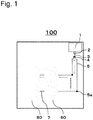
Figs. 1 and2 are schematic top views that show prior-art optical integrated circuits for optical transmitters placed on opto-electric hybrid boards. InFig. 1 , arrangement of typical optical elements such as optical waveguide elements and so on is shown. On the other hand, inFig. 2 , optical waveguide elements and so on are not shown; however, instead thereof, arrangement of circuit elements such as input pads (electrically conductive pins in this example) for high-speed electric signals, a driver IC, and so on is shown. This type of optical integrated circuit can be downsized and made to be highly dense by forming it within a silicon substrate by using the silicon photonics technique. - In an optical integrated
circuit 100 inFig. 1 , the laser light, that is emitted by asemiconductor laser 1 and inputted via optical coupling, propagates through an optical waveguide 3 via aspot size converter 2; and the laser light is coupled to a coupler (an MMI coupler) 4. In the optical coupler 4, the laser light is divided into plural pieces of input light, and the pieces of the input light propagate throughoptical waveguides 5a that are constructed as curved waveguides havingcurved parts 5a; and the pieces of the input light are inputted to anoptical modulator array 60 in which plural optical modulators are arranged. The optical signals outputted from theoptical modulator array 60 are coupled, viaoptical waveguides 7, to an optical signaloutputting element array 80 in which plural optical signal outputting elements are arranged; and the optical signals are outputted from the optical signal outputting elements to the outside via optical fibers and so on. - As shown in
Fig. 2 , in an opto-electric hybrid board, an electric I/O array 90 that is formed by arranging, along fringe parts of the board, plural input pads for electrical connection for high-speed electric signals, and adriver IC 50 for controlling optical modulation are placed; andelectrical connecting wires 95 of high-speed electric wiring are further formed on the opto-electric hybrid board. On the opto-electric hybrid board, the area for placing thedriver IC 50 overlaps with the area of theoptical modulator array 60; the driver IC is placed above the optical modulator; and the direction of propagation of the light within the optical modulator and the direction of propagation of the electric signal within the driver IC coincide with each other. Thus, thelaser 1 is placed in such a manner that it avoids the electric I/O array 90 and the electrical connecting wires (in this example, it is placed on a corner part of the plane). - Although the above is shown as an example of an optical integrated circuit for an optical transmitter, an example of a transmission unit in an optical transmitted/received is similar to that described above.
- Non-patent-related Document 1: "Demonstration of 12.5-Gbps optical interconnects integrated with lasers, optical splitters, optical modulators and photodetectors on a single silicon substrate," OPTICS EXPRESS, Vol. 20, No. 26 (2012/12/10) B256-B263
- Document
US 2012/15588 A1, 21 June 2012 , relates to an optical modulator that includes a light input /output unit receiving an incident optical signal which has not been modulated, splitting the incident optical signal into a first optical signal and the second optical signal and transmitting the first and second optical signals to a first path and a second path respectively of an optical waveguide. A phase shifter is positioned in one of the first and second paths and modulates a phase of at least one of the first and second optical signals, which have been received through the first and second paths, respectively, in response to an electrical signal. A phase modulated signal is output. A reflective grating coupler reflects signals respectively received through the first and second paths back along the first and second paths respectively. - Document
US 2011/274438 A1, 10 November 2011 , relates to an optical engine for providing a point-to-point communication link between devices. - Document
US 2006/210215 A1 relates to board level optical system for high speed device interconnection. - As explained above, in the prior-art optical integrated circuit provided on the opto-electric hybrid board, the placement of the
semiconductor laser 1 is determined in such a manner that thesemiconductor laser 1 is placed to avoid the electric I/O array 90 and the electrical connecting wires (it is placed on a corner part of the plane in each ofFigs. 1 and2 ). Thus, in the case that the number of channels is increased for the purposes of further downsizing and densification, arrangement of electric wiring will become difficult. Further, since the semiconductor laser is to be avoided when electric wiring is carried out, it may be necessary to bend an electric wiring line to have a bend angle of 90 degrees or more with respect to the propagation direction of electricity within the driver IC; so that deterioration of an electric signal cannot be avoided, as the speed of a signal for each channel increases. Still further, in the case that the semiconductor laser is placed on the corner part of the plane on the opto-electric hybrid board, and coupled to the optical modulator by use of the optical wave guide with the shortest distance therebetween, there is a problem such that, regarding theoptical waveguides 5 arranged between thesemiconductor laser 1 and theoptical modulator array 60, their line lengths are largely different between respective channels. - In general, input light attenuates due to the length of an optical wave guide. Especially, in a multi-channel operation, if the degrees of intensity of pieces of input light at a receiving side are different for respective channels, crosstalk is likely generated due to differences of amplification ratios for respective channels in the receiver. Thus, it is not preferable to use optical waveguides having different lengths for respective channels.
- This problem is solved with the subject-matter of the
independent claim 1. Advantageous embodiments are described in the dependent claims. In an aspect, the present invention provides an optical transmitter that comprises an optical integrated circuit that is characterized in placement of a single-channel or multi-channel semiconductor laser and arrangement of optical waveguides. - An optical transmitter provided on an opto-electric hybrid board comprises a semiconductor laser for emitting laser light by use of plural channels; optical waveguides, coupled respectively and optically to the semiconductor laser, for allowing pieces of the laser light for the respective channels to propagate through the optical waveguides as pieces of input light; optical modulators for generating optical signals by modulating the pieces of input light; and optical signal outputting parts, respectively coupled to the optical modulators, for outputting the optical signals propagated through the optical modulators to the outside. On a plane of the opto-electric hybrid board, the semiconductor laser is placed on a side of the optical signal outputting parts opposite to another side of the optical signal outputting parts where the optical modulators are placed.
- Also, the optical transmitter provided on the opto-electric hybrid board of the present invention comprises optical branching units, wherein each of the optical branching units divides the laser light into two or more pieces of input light, and the modulators are respectively coupled to two or more optical output terminals provided to the optical branching unit.
- In the optical transmitter provided on the opto-electric hybrid board of the present invention, each of the optical signal outputting parts comprises a grating coupler for diffracting the propagated optical signal, and an optical pin optically coupled to the grating coupler and installed to stand with a desired angle with respect to a plane of the opto-electric hybrid board for outputting the optical signal to the outside.
- Further, in the optical transmitter provided on the opto-electric hybrid board of the present invention, the semiconductor laser comprises m channels (m is an integer that is equal to or more than 1), the optical waveguides comprise first to m-th optical waveguides, the optical branching units comprise first to m-th optical branching units, each of the first to m-th optical branching units divides the laser light into n pieces of input light (n is any integer that is equal to or more than 2), the n pieces of input light are coupled via the optical output terminals to first to n-th optical modulators, a k-th optical waveguide (k is any integer that is equal to 1 or m, or between 1 and m) is coupled to a k-th optical branching unit through a space between an n-th optical modulator coupled to a (k-1)th optical branching unit and a first optical modulator coupled to the k-th optical branching unit, or a space between an n-th optical modulator coupled to the k-th optical branching unit and a first optical modulator coupled to a (k+1)th optical branching unit, for making the connection length of each of the plural optical waveguides to be equal.
- According to the basic construction of the present invention, in the optical transmitter provided on the opto-electric hybrid board, the semiconductor laser is placed on an output side of the optical modulators, i.e., it is placed near the optical signal outputting parts, in the optical integrated circuit; so that electric wire connection of electrical signal wiring lines, that is highly dependent on frequencies, can be carried out more effectively and freely. Thus, load on the electric wiring for high-speed/high-frequency use can be reduced. Further, by having an optical pin as an optical interface, deterioration of the above explained electrical wiring can be suppressed, and low-loss coupling to an external waveguide such as a fiber or the like can be carried out without having effect due to placement of the semiconductor laser and/or the driver IC. By guiding the light from the semiconductor laser to the optical modulators by use of optical waveguides that are placed in spaces between optical modulators, and by making the connection length of each of the plural optical waveguides to be equal the optical waveguides to be isometric, the wiring length can be reduced, uniformity of optical losses can be realized, crosstalk in the receiver side can be suppressed, and optical interconnection having good signal quality can be realized, when compared with the case that wiring is carried out to avoid the driver IC and/or the whole of optical modulators.
- As a result, the present invention can realize an optical transmitter having good high-frequency characteristics.
-
-
Fig. 1 is a schematic plain view showing a prior-art optical integrated circuit for an optical transmitter (or a transmission unit in an optical transmitter/receiver). -
Fig. 2 is a schematic plain view showing a prior-art optical integrated circuit for an optical transmitter. -
Fig. 3 is a schematic plain view of showing optical integrated circuit for an optical transmitter according to an embodiment of the present invention. -
Fig. 4 is a schematic plain view showing an optical integrated circuit for an optical transmitter according to an embodiment of the present invention. -
Fig. 5 is a schematic plain view showing an optical integrated circuit for an optical transmitter according to an embodiment of the present invention. -
Fig. 6 is a cross-section view of an optical integrated circuit for an optical transmitter according to an embodiment of the present invention. -
Fig. 7 is a schematic view for explaining an embodiment of arrangement of respective optical elements in an optical integrated circuit for an optical transmitter according to an embodiment of the present invention. -
Fig. 8 shows an example of arrangement of optical elements, that is based onFig. 7 , in an optical integrated circuit for an optical transmitter according to an embodiment of the present invention. -
Fig. 9 shows an example of arrangement of optical elements, that is based onFig. 7 , in an optical integrated circuit for an optical transmitter according to an embodiment of the present invention. -
Fig. 10 shows an example of arrangement of optical elements, that is based onFig. 7 , in an optical integrated circuit for an optical transmitter according to an embodiment of the present invention. -
Fig. 11 shows an example of arrangement of optical elements, that is based onFig. 7 , in an optical integrated circuit for an optical transmitter according to an embodiment of the present invention. -
Fig. 12 shows an example of arrangement of optical elements for an optical transmitter according to a different embodiment of the present invention. - In the following, an optical transmitter provided on an opto-electric hybrid board according to each of embodiments of the present invention will be explained in detail with reference to the figures. Similar reference symbols are assigned to similar components.
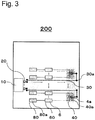
- Each of
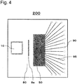
Figs. 3-5 is a schematic plain view showing an opticalintegrated circuit 200 for an optical transmitter provided on an opto-electric hybrid board, according to an embodiment of the present invention.Fig. 3 shows an aspect of arrangement of optical elements; and this figure corresponds toFig. 1 that shows a prior-art construction. On the other hand,Fig. 4 does not show optical waveguide elements and so on; however, instead thereof, it shows arrangement of circuit elements such as input pads (electrically conductive pins in this example) for high-speed electric signals, a driver IC, and so on.Fig. 4 corresponds toFig. 2 that shows a prior-art construction. - As shown in
Fig. 3 , the opticalintegrated circuit 200 for an optical transmitter according to an embodiment of the present invention comprises: a single-channel ormulti-channel semiconductor laser 10 for emitting laser light by use of one or more channels;optical waveguides 30, that are coupled optically from thesemiconductor laser 10 viaspot size converters 20 for respective channels, for sending laser light to be propagated in a lateral direction mainly; optical branchingparts 40a that are respectively coupled to theoptical waveguides 30, and compriseoptical couplers 4a for dividing the laser light into at least two pieces of input light;optical modulators 6, that are respectively coupled to two or more optical output terminals provided to the respective optical branching parts, for generating optical signals by modulating the pieces of input light; and opticalsignal outputting parts 80a, that are respectively coupled to theoptical modulators 6, for outputting the optical signals propagated through the optical modulators to the outside. - The plural optical branching
parts 40a comprisingoptical couplers 4a are aligned in a line in a longitudinal direction to thereby form anoptical coupler array 40; the pluraloptical modulators 6 are aligned in a line in a longitudinal direction to thereby form anoptical modulator array 60; and the plural opticalsignal outputting parts 80a are aligned in a line in a longitudinal direction to thereby form an opticalsignal outputting array 80. - In a plane of the opto-
electric hybrid board 200, thesemiconductor laser 10 is placed on a side of the opticalsignal outputting parts 80a (optical signal outputting array 80) opposite to another side of the opticalsignal outputting parts 80a where the optical modulators 6 (optical modulator array 60) are placed. - In this embodiment, although the optical branching
parts 40a (optical coupler array 40) are placed on a side of the optical modulators 6 (optical modulator array 60) opposite to another side of the optical modulators 6 (optical modulator array 60) where thesemiconductor laser 10 is placed, it is possible to place the optical branchingparts 40a (optical coupler array 40) in a space between thesemiconductor laser 10 and the opticalsignal outputting parts 80a (optical signal outputting array). Regarding the optical branchingparts 40a (optical coupler array 40) and the electrical connectingwires 95 for high-speed signals, it should be noted that, since the electrical connectingwires 95 can be formed on the optical branchingparts 40a (optical coupler array 40) and they do not interfere with each other, the optical branchingparts 40a (optical coupler array 40) are placed on a side of the optical modulators 6 (optical modulator array 60) opposite to another side of the optical modulators 6 (optical modulator array 60) where thesemiconductor laser 10 is placed; this is because the size of the area of the chip can be reduced and the area to be used for electrical wiring can be increased. - When compared with
Fig. 1 that shows a prior-art construction, it can be found that the construction such that thesemiconductor laser 10 is placed on an output side of the optical modulators 6 (optical modulator array 60), specifically, on the opticalsignal outputting array 80 side, is greatly different from the prior-art construction; and it can be found that the construction such that theoptical waveguides 30 from thespot size converters 20 are connected to the optical branchingparts 40a, that are placed on a side opposite to another side where thesemiconductor laser 10 is placed, by placing theoptical waveguides 30 in spaces between adjacentoptical modulators 6 to extend laterally is also different from the prior-art construction. Note that, although thesemiconductor laser 10 shown in the figure is a multi-channel semiconductor laser, the semiconductor laser to be used is not limited so; and a single-channel semiconductor laser such as that shown inFig. 1 can be also used. - The placement of the
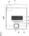
semiconductor laser 10 on the opto-electric hybrid board will become more apparent after referring toFigs. 4 and5 . Specifically, in the optical transmitter according to the present embodiment, thesemiconductor laser 10 is placed on the opticalsignal outputting array 80 side that is located on the left side (not the electrical I/O array 90 side) in the optical integrated circuit. As a result, the semiconductor laser placing area (area Za shown by a dashed line inFig. 5 ), that was required in the prior-art technique, can be reserved as a space that is to be used as an area for arranging input pads and an area for electrical connecting wires for high-speed electric wiring directed from the input pads to thedriver IC 50, as shown inFig. 4 . Thus, electric connection of high-speed electric wiring lines can be carried out more freely by using the area wider than the area provided by the prior-art technique. - Further, in the aspect of the arrangement of elements shown in each of
Figs, 4 and5 ,optical pins 8a are provided as the opticalsignal outputting parts 80a included in the optical transmitter according to the present embodiment. More specifically, each of the opticalsignal outputting parts 80a is constructed to comprise agrating coupler 8b for diffracting the optical signal propagated through theoptical modulator 6, and anoptical pin 8a optically coupled to thegrating coupler 8b and installed to stand with a desired angle with respect to the plane of the opto-electric hybrid board for outputting the optical signal to the outside. By constructing the opticalsignal outputting part 80a as explained above, there will be an advantage such that the optical fiber array placing area (area Zb shown by a dashed line inFig. 5 ), that was provided for connection with optical fibers and so on, can be reserved and used as a space for placing the semiconductor laser. - Further, when compared with the prior-art optical
integrated circuit plane 100 shown inFig. 1 (this area corresponds to area Z represented by dashed line inFig. 5 ), it can be understood that, in the integratedcircuit plane 200 for the optical transmitter according to the present embodiment shown inFig. 5 , by changing thesemiconductor laser 10 placing area from the prior-art area (Za), it becomes possible to slightly shift the whole of the opto-electric hybrid board plane in a lateral direction with respect to thedriver IC 50 and/or the optical signal outputting array 80 (the left arrow represented by a dashed line). As a result, a space that is newly set below thesemiconductor laser 10 placing area (area Zc shown by a dashed line inFig. 5 ) can be used as a new placing space for electric wiring. For example, it becomes possible to newly reserve and use it as a space for placing control pads (not shown) for inputting and/or outputting low-speed modulation control signals. Thus, it becomes possible to further separate a low-speed electric wiring area and a high-speed electric wiring area, so that it becomes possible to realize further effective electric signal wiring. -
Fig. 3 will be referred to again. In the optical transmitter according to the present embodiment, the pluraloptical waveguides 30 are arranged in such a manner that each of them comprises a curved waveguide having acurved part 30a, and extends through a space between predetermined adjacent optical modulators, for making the length of each of the optical waveguides to be equal with each other (i.e., for realizing isometric). By arranging theoptical waveguides 30 in such a manner, isometic of optical waveguides can be realized with shorter wiring length, compared with, for example, the case that theoptical waveguides 30 are placed in a periphery of theoptical modulator array 60 and the opticalsignal outputting array 80 for avoiding them. Note that, throughout the present invention, the optical waveguides are constructed to comprise longitudinal waveguides, lateral waveguides, and curved parts for bending the waveguides by 90 degrees. - Next, supplementary explanation of arrangement of optical waveguides between adjacent optical modulators will be provided. In general, the size of the optical modulator used in the optical integrated circuit with a scale of a 5 µm x 5 µm, that is formed by use of the silicon photonics technique, is approximately 40 µm x 250 µm, and the pitch between adjacent optical modulators is approximately 125 µm. In this regard, a blank space of approximately 85 µm exists between the adjacent optical modulators. If it is supposed that the core diameter of the optical waveguide is 3 µm, and a clad on each of both sides thereof is 1 µm, it is possible to place approximately 20 optical waveguides between the adjacent optical modulators.
- As explained above, in the optical
integrated circuit 200 in the optical transmitter of the present invention, by placing the semiconductor laser on the output side of the optical modulators, i.e., on a place near the optical signal outputting parts, and by contriving arrangement of optical waveguides, that are less dependent on frequencies, to achieve isometric, it becomes possible to carry out arrangement of high-speed electric wiring lines, that is highly dependent on frequencies, more effectively and freely, and reduce the load on the electric wiring. -
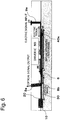
Fig. 6 is a cross-section view of an optical integrated circuit for an optical transmitter according to an embodiment of the present invention. An aspect of an operation at the time of optical signal transmission will be explained with reference toFig. 6 . The laser light from thesemiconductor laser 10 placed on the side of the optical outputting parts is inputted to theoptical modulator 6 via thespot size converter 20, theoptical waveguide 30, the optical branchingpart 40a on the side of the electrically conductive pin 9a, and so on ((i)-(iii)); and a modulated optical signal is outputted by the optical modulator 6 (iv). The modulated optical signal arrives at thegrating coupler 8b via the optical waveguide, the optical axis is changed by diffraction by thegrating coupler 8b, and the resultant optical signal is outputted to the outside via theoptical pin 8a (v). Note that the electric signal inputted from the outside via the electrically conductive pin 9a is inputted to the driver IC for controlling theoptical modulator 6 and the semiconductor laser 10 ((I)-(II)), and supplied as a modulation controlling signal (an electric signal) to theoptical modulator 6 via the electric wiring (III). - In the following, with reference to
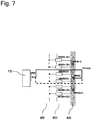
Fig. 7 , the arrangement of the respective optical elements, i.e., the arrangement of thesemiconductor laser 10 placed on the side of the opticalsignal outputting array 80 and the optical couplers 4 (optical branchingparts 40a) placed on the side of the electrical I/O array 90 (not shown in the drawing), for the optical transmitter according to an embodiment of the present invention will be further explained in detail. For convenience, the channel number of the m-channel semiconductor laser 10 is represented by the expression CH[k] (in this embodiment, it is supposed that a multi-channel semiconductor laser is used; and m is an integer that is equal to or more than 2, and k is any integer that is equal to 1 or m, or between 1 and m), and the optical waveguide and the optical coupler related to the CH[k] are represented by the expressions PATH[k] and MMI[k], respectively. - As shown in the figure, in the
optical coupler array 40, the optical couplers MMI[k-1], MMI[k], and MMI[k+1] are aligned in a line in a longitudinal direction. The optical coupler MMI[k] divides the laser light into n pieces of input light (n is an integer that is equal to or more than 2), and couples the light via its output terminals to the n optical modulators, respectively. Note that, although the optical coupler MMI[k] comprises one stage inFig. 7 , the construction is not limited thereto. For example, as shown inFigs. 8-11 that will be referred to later, it is possible to construct the optical branchingunit 40a comprising theoptical couplers 4a that are arranged in a multiple stage structure comprising two or more stages. - In addition, n optical modulators coupled to the optical coupler MMI[k] are represented by the expressions MOD[k][1]-MOD[k][n]. As shown in the figure, in the
optical modulator array 60, the optical modulators MOD[k-1][1] - MOD[k-1][n], MOD[k][1] - MOD[k][n], and MOD[k+1][1] - MOD[k+1][n] are aligned in a line in a longitudinal direction. - As shown in
Fig. 7 , for realizing isometric, the optical waveguide PATH[k] arranged between specified adjacent optical modulators is placed in such a manner that it is arranged to couple to the optical coupler MMI[k] through one of the space between the optical modulator MOD[k-1][n] coupled to the optical coupler MMI[k-1] and the optical modulator MOD[k][1] coupled to the optical coupler MMI[k] (the solid line), and the space between the optical modulator MOD[k][n] coupled to the optical coupler MMI[k] and the optical modulator MOD[k+1][1] coupled to the optical coupler MMI[k+1] (the broken line). - Note that the top optical waveguide PATH[1] would be arranged in such a manner that it extends through the space between the optical modulator MOD[1][n] coupled to the optical coupler MMI[1] and the optical modulator MOD[2][1] coupled to the optical coupler MMI[2], and the bottom optical waveguide PATH[m] would be arranged in such a manner that it extends through the space between the optical modulator MOD[m][n] coupled to the optical coupler MMI[m-1] and the optical modulator MOD[m][1] coupled to the optical coupler MMI[m].
- In the following, with reference to each of
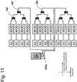
Figs. 8-11 , an example of arrangement of optical elements based onFig. 7 , in an integrated circuit for an optical transmitter according to each embodiment of the present invention, will be explained. Each ofFigs. 8-11 has 12-channel optical output, for example; that is, 12 pairs, each comprising a grating coupler (represented by the expression "GC" in the figure) and an optical pin (not shown in the drawing), are aligned. Similarly, 12 optical modulators (represented by the expression "MOD" in the figure) are also aligned. In these embodiment,Fig. 8 is an example using a 2-channel semiconductor laser,Fig. 9 is an example using a 3-channel semiconductor laser, andFig. 10 is an example using a single-channel semiconductor laser. - In
Fig. 8 , the optical output comprises 12 channels for the 2-channel semiconductor laser (LD); thus, the 12 optical modulators are divided into groups, each comprising 6 optical modulators; and twooptical waveguides 30 are arranged between adjacent optical modulators between the groups, based onFig. 7 . Further, by constructing optical branchingparts 40a to comprise two-stage arrangement comprising 2-branch-typeoptical couplers 4a' and 3-branch-typeoptical couplers 4a", the laser light outputted from each channel is divided into 6 pieces of input light. - Similarly, in
Fig. 9 , the optical output comprises 12 channels for the 3-channel semiconductor laser (LD); thus, the 12 optical modulators are divided into groups, each comprising 4 optical modulators; and oneoptical waveguide 30 or twooptical waveguides 30 is/are arranged between adjacent optical modulators between the groups, based onFig. 7 . Further, by constructing optical branchingparts 40a to comprise two-stage arrangement comprising 2-branch-typeoptical couplers 4a', the laser light outputted from each channel is divided into 4 pieces of input light. - As would be understandable from
Figs. 8 and9 , for achieving isometric of optical waveguides between the optical branchingparts 40a and theoptical modulators 6, in addition to arranging theoptical waveguides 30 between thesemiconductor laser 10 and the optical branchingparts 40a to achieve isometric thereof, it is desirable to construct each optical branchingpart 40a in such a manner that it comprises multi-stage arrangement comprising plural 2-branch-type or 3-branch-type optical couplers to divide the laser light into an arbitrary number of pieces of input light; however, the construction is not limited to the above, that is, single-stage arrangement comprising 4-branch optical couplers and so on may be used as long as isometric can be realized. Note that, inFig. 8 , for achieving isometric wiring of the optical waveguides between the 3-branch-type optical couplers and the optical modulators, the optical waveguides are appropriately devised to comprisecurved parts 30a'; however, any types of arrangement of curved parts can be accepted as long as isometric of the optical waveguides can be realized. - Note that, in the case that the semiconductor laser is a single-channel-type semiconductor laser, it is constructed in such a manner that one
optical waveguide 30 is placed in the center of the optical modulator array 60 (i.e., between the optical modulator groups, each being grouped to comprise 6 optical modulators), and that the optical branchingpart 40a comprises three-stage arrangement comprising 2-branch-type optical couplers and 3-branch-type optical couplers, as shown inFig. 10 . As a result, the waveguide length can be made to be shorter than that in the case that theoptical waveguide 30 is arranged on the periphery of theoptical modulator array 60. -
Fig. 11 shows a further modified example of arrangement of the optical elements shown inFig. 9 . Compared withFig. 9 , the direction of emission of laser light from the semiconductor laser (LD) is changed inFig. 11 . Specifically, the optical waveguide for each channel, that is arranged as a curved waveguide comprising acurved part 30a, extends from the spot size converter in a longitudinal direction, that is orthogonal to a lateral direction from thesemiconductor laser 10 to the optical signal outputting array 80 (i.e., the direction to the optical signal outputting parts (GC)), and, at thecurved part 30a positioned at a predetermined distance from thesemiconductor laser 10, curves 90 degrees in a direction toward the optical signal outputting parts (i.e., the lateral direction). A reason to construct the optical elements as explained above is to prevent harmful influences on the optical integrated circuit and other elements and devices, due to stray light that is generated when end surfaces of the semiconductor laser and the spot size converter are coupled, confined within the clad, and reflected within the clad and thus guided to propagate therethrough. In this case, it is preferable to set the distance in relation to intensity of signal light. As an example, it is considered to set, as a predetermined distance, a distance that makes the intensity of the stray light relative to the optical signal propagating through the optical waveguide to be -30 dB. - Note that, although
Fig. 11 is presented as a modified example ofFig. 9 , explanations similar to those applied thereto also apply to other arrangement examples. - In each of the examples of arrangement of the elements shown in
Figs. 7-11 , it is explained based on a precondition such that the optical branchingparts 40a comprising theoptical couplers 4a are formed in such a manner that they are aligned in a line in a longitudinal direction; however, it should be natural that a person skilled in the art admits that such optical branchingparts 40a comprising theoptical couplers 4a are not necessary components. - More specifically, compared with
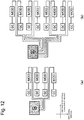
Fig. 11 , an aspect that does not have the construction relating to the optical branchingparts 40a comprising theoptical couplers 4a, such as each of examples of arrangement of elements shown inFig. 12 , is possible. The example of (a) inFig. 12 depicts a case of 4 channels, and the example of (b) inFig. 12 depicts a case of 8 channels. That is, it is possible to construct in such a manner that the optical waveguides are coupled respectively from the semiconductor laser to the optical modulators via the spot size converters, wherein the number of spot size converters is equal to that of the channels; and that the laser light (input light) is directly inputted to the optical modulators. In the case that plural channels exist and the number of the channels is a multiple of 2 as is the case with each of the arrangement examples shown inFig. 12 , it should be noted that it is possible to arrange the plural optical waveguides in such a manner that the respective wiring lengths of the plural optical waveguides, that are waveguides including curved parts, are made to be approximately equal with each other (i.e., isometric is to be realized), by considering two channels as a pair. - Further, regarding arrangement of optical waveguides, although it is needles to explain, it is possible to construct the whole of the arrangement by combining the aspect of the arrangement for the case that the optical branching
part 40a is used such as the case shown inFig. 11 , and the aspect of the arrangement for the case that the optical branchingpart 40a is not used such as the case shown inFig. 12 . - In the above, the present invention has explained in detail with reference to the drawings; and a person skilled in the art would understand that other similar embodiments can be used, and that modification of an embodiment or addition of an embodiment can be carried out without departing from the present invention. Note that the present invention should not be limited to the above embodiments; and the present invention should be construed based on the descriptions of the claims.
-
- Optical
integrated circuit -
Semiconductor laser -
Spot size converter -
Optical coupler -
Optical coupler array 40 - Optical branching
unit 40a -
Optical waveguide -
Curved part -
Optical modulator 6 -
Optical modulator array 60 -
Optical pin 8a -
Grating coupler 8b - Optical
signal outputting array 80 -
Optical output part 80a - Electrically conductive pin 9a
- Electrical I/
O array 90 - Electrical connecting
wire 95 -
Driver IC 50
Claims (4)
- An optical transmitter provided on an opto-electric hybrid board comprising:a semiconductor laser (10) for emitting laser light by use of plural channels; optical waveguides (30), coupled respectively and optically to the semiconductor laser (10), for allowing pieces of the laser light for the respective channels to propagate through the optical waveguides (30) as pieces of input light; optical modulators (6) for generating optical signals by modulating the pieces of input light; optical signal outputting parts (80a), respectively coupled to the optical modulators (6), for outputting the optical signals propagated through the optical modulators (6) to the outside; and optical branching units (40a), wherein each of the optical branching units (40a) divides the laser light into two or more pieces of input light, and the modulators (6) are respectively coupled to two or more optical output terminals provided to the optical branching unit (40a),wherein on a plane of the opto-electric hybrid board, the semiconductor laser (10) is placed on a side of the optical signal outputting parts (80a) opposite to another side of the optical signal outputting parts (80a) where the optical modulators (6) are placed, characterized in that the optical branching units (40a) are placed on a side of the optical modulators (6) opposite to another side of the optical modulators (6) where the semiconductor laser (10) is placed.
- The optical transmitter according to Claim 1, wherein it is characterized in that each of the optical signal outputting parts (80a) comprises a grating coupler (8b) for diffracting the propagated optical signal, and an optical pin (8a) optically coupled to the grating coupler and installed to stand with a desired angle with respect to a plane of the opto-electric hybrid board for outputting the optical signal to the outside.
- The optical transmitter according to Claim 1, wherein it is characterized in that
the semiconductor laser (10) comprises m channels, m is an integer that is equal to or more than 1, the optical waveguides (30) comprise first to m-th optical waveguides (30), and the optical branching units (40a) comprise first to m-th optical branching units (40a),
each of the first to m-th optical branching units (40a) divides the laser light into n pieces of input light, n is any integer that is equal to or more than 2, and the n pieces of input light are coupled via the optical output terminals to first to n-th optical modulators (6), and
a k-th optical waveguide (30), k is any integer that is equal to 1 or m, or between 1 and m, is coupled to a k-th optical branching unit (40a) through a space between an n-th optical modulator (6) coupled to a (k-1)th optical branching unit (40a) and a first optical modulator (6) coupled to the k-th optical branching unit (40a), or a space between an n-th optical modulator (6) coupled to the k-th optical branching unit (40a) and a first optical modulator (6) coupled to a (k+1)th
optical branching unit (40a), for making the connection length of each of the plural optical waveguides (30) to be equal. - The optical transmitter according to Claim 1 or 3, wherein it is characterized in that each of the optical branching units (40a) comprises plural two-branch optical couplers (4a') or plural three-branch optical couplers (4a") arranged in multiple stages for dividing the laser light into any number of pieces of input light.
Applications Claiming Priority (2)
| Application Number | Priority Date | Filing Date | Title |
|---|---|---|---|
| JP2013151491 | 2013-07-22 | ||
| PCT/JP2014/069164 WO2015012213A1 (en) | 2013-07-22 | 2014-07-18 | Transmission unit for optical transmitter/receiver or optical transmitter provided to opto-electric hybrid board |
Publications (3)
| Publication Number | Publication Date |
|---|---|
| EP3026472A1 EP3026472A1 (en) | 2016-06-01 |
| EP3026472A4 EP3026472A4 (en) | 2017-03-22 |
| EP3026472B1 true EP3026472B1 (en) | 2019-04-10 |
Family
ID=52393254
Family Applications (1)
| Application Number | Title | Priority Date | Filing Date |
|---|---|---|---|
| EP14829257.6A Active EP3026472B1 (en) | 2013-07-22 | 2014-07-18 | Optical transmitter provided to opto-electric hybrid board |
Country Status (4)
| Country | Link |
|---|---|
| US (1) | US9577407B2 (en) |
| EP (1) | EP3026472B1 (en) |
| JP (1) | JP6532403B2 (en) |
| WO (1) | WO2015012213A1 (en) |
Families Citing this family (5)
| Publication number | Priority date | Publication date | Assignee | Title |
|---|---|---|---|---|
| US9612401B2 (en) | 2015-02-18 | 2017-04-04 | Ciena Corporation | Method and system for providing optical connections |
| CN105319658A (en) * | 2015-11-13 | 2016-02-10 | 宁波环球广电科技有限公司 | Multi-channel-parallel optical transceiver |
| JP6183527B1 (en) * | 2016-09-30 | 2017-08-23 | 富士通オプティカルコンポーネンツ株式会社 | Optical module and optical modulator |
| US10527854B1 (en) * | 2018-06-18 | 2020-01-07 | Facebook Technologies, Llc | Illumination source for a waveguide display |
| JP2022115723A (en) * | 2021-01-28 | 2022-08-09 | アイオーコア株式会社 | Photoelectric module |
Family Cites Families (13)
| Publication number | Priority date | Publication date | Assignee | Title |
|---|---|---|---|---|
| JPS62206996A (en) * | 1986-03-07 | 1987-09-11 | Hitachi Ltd | Light replacing method and device therefor |
| US5835646A (en) * | 1995-09-19 | 1998-11-10 | Fujitsu Limited | Active optical circuit sheet or active optical circuit board, active optical connector and optical MCM, process for fabricating optical waveguide, and devices obtained thereby |
| DE10112274B4 (en) * | 2001-03-14 | 2006-05-24 | Finisar Corp.(N.D.Ges.D.Staates Delaware), Sunnyvale | Optoelectronic transmission module and method for its production |
| US6912333B2 (en) * | 2002-06-21 | 2005-06-28 | Fujitsu Limited | Optical interconnection apparatus and interconnection module |
| JP2005266623A (en) * | 2004-03-22 | 2005-09-29 | Tokai Univ | Optical printed board |
| US20060210215A1 (en) * | 2005-03-15 | 2006-09-21 | Shigenori Aoki | Optical transceiver array |
| WO2007013128A1 (en) | 2005-07-25 | 2007-02-01 | Fujitsu Limited | Semiconductor chip module |
| US7940828B2 (en) * | 2006-02-24 | 2011-05-10 | Nec Corporation | Optical communication system and optical transmitter |
| KR101520143B1 (en) * | 2009-01-09 | 2015-05-13 | 휴렛-팩커드 디벨롭먼트 컴퍼니, 엘.피. | Optical engine for point-to-point communications |
| US8515217B2 (en) * | 2009-09-02 | 2013-08-20 | Alcatel Lucent | Vertical optically emitting photonic devices with electronic steering capability |
| JP5467826B2 (en) * | 2009-09-16 | 2014-04-09 | 日東電工株式会社 | Opto-electric hybrid module and manufacturing method thereof |
| JP2011085647A (en) * | 2009-10-13 | 2011-04-28 | Hitachi Chem Co Ltd | Optical waveguide substrate and method for manufacturing the same |
| KR101845514B1 (en) * | 2010-12-17 | 2018-04-04 | 삼성전자주식회사 | Optical modulator with reduced size and optical transmitter having the same |
-
2014
- 2014-07-18 JP JP2015528267A patent/JP6532403B2/en active Active
- 2014-07-18 EP EP14829257.6A patent/EP3026472B1/en active Active
- 2014-07-18 WO PCT/JP2014/069164 patent/WO2015012213A1/en active Application Filing
- 2014-07-18 US US14/906,880 patent/US9577407B2/en active Active
Non-Patent Citations (1)
| Title |
|---|
| None * |
Also Published As
| Publication number | Publication date |
|---|---|
| US20160164251A1 (en) | 2016-06-09 |
| JPWO2015012213A1 (en) | 2017-03-02 |
| EP3026472A1 (en) | 2016-06-01 |
| WO2015012213A1 (en) | 2015-01-29 |
| JP6532403B2 (en) | 2019-06-19 |
| EP3026472A4 (en) | 2017-03-22 |
| US9577407B2 (en) | 2017-02-21 |
Similar Documents
| Publication | Publication Date | Title |
|---|---|---|
| EP3026472B1 (en) | Optical transmitter provided to opto-electric hybrid board | |
| KR102009979B1 (en) | Semiconductor package and semiconductor device including the same | |
| US7536066B2 (en) | Semiconductor chip module | |
| US20100266295A1 (en) | Optical-signal-path routing in a multi-chip system | |
| CN110830119B (en) | Optical module | |
| CN103814314A (en) | Optical module | |
| US20170123173A1 (en) | Optical Integrated Circuit Package | |
| CN116964501A (en) | Method for co-packaging optical modules on a switch package substrate | |
| JP2012047855A (en) | Light input/output structure for multilayer optical wiring | |
| US8363989B2 (en) | Semiconductor optical interconnection device and semiconductor optical interconnection method | |
| US20190361173A1 (en) | Semiconductor device | |
| JP2010225991A (en) | Multi-wavelength laser device | |
| CN218213537U (en) | Multichannel optical transceiving component and optical module | |
| CN114594554A (en) | Optical module | |
| JP2005091460A (en) | Bidirectional optical module, optical transmitter and receiver and optical transmission system | |
| JP6542668B2 (en) | Transmitter of an optical transmitter or an optical transmitter / receiver provided on an optical / electrical hybrid board | |
| JP7433545B1 (en) | Laser beam emitting device and optical module | |
| Lee et al. | Increasing bandwidth density in future optical interconnects | |
| WO2014156959A1 (en) | Optical end coupling type silicon optical integrated circuit | |
| CN117438419A (en) | Semiconductor package and data transmission method of semiconductor package | |
| WO2005096052A1 (en) | Light wave circuit module | |
| KR20240066812A (en) | Microscale Multi-functional Optical Structure | |
| JPH10135911A (en) | Optical signal distribution printed circuit board | |
| KR101265754B1 (en) | optical waveguide device | |
| JP2012080341A (en) | Directivity-controlled base station antenna |
Legal Events
| Date | Code | Title | Description |
|---|---|---|---|
| PUAI | Public reference made under article 153(3) epc to a published international application that has entered the european phase |
Free format text: ORIGINAL CODE: 0009012 |
|
| 17P | Request for examination filed |
Effective date: 20160121 |
|
| AK | Designated contracting states |
Kind code of ref document: A1 Designated state(s): AL AT BE BG CH CY CZ DE DK EE ES FI FR GB GR HR HU IE IS IT LI LT LU LV MC MK MT NL NO PL PT RO RS SE SI SK SM TR |
|
| AX | Request for extension of the european patent |
Extension state: BA ME |
|
| DAX | Request for extension of the european patent (deleted) | ||
| A4 | Supplementary search report drawn up and despatched |
Effective date: 20170221 |
|
| RIC1 | Information provided on ipc code assigned before grant |
Ipc: G02B 6/122 20060101AFI20170215BHEP Ipc: H01S 5/022 20060101ALI20170215BHEP Ipc: G02B 6/28 20060101ALI20170215BHEP Ipc: H01S 5/026 20060101ALI20170215BHEP Ipc: G02B 6/42 20060101ALI20170215BHEP |
|
| RAP1 | Party data changed (applicant data changed or rights of an application transferred) |
Owner name: AIO CORE CO., LTD. |
|
| STAA | Information on the status of an ep patent application or granted ep patent |
Free format text: STATUS: EXAMINATION IS IN PROGRESS |
|
| 17Q | First examination report despatched |
Effective date: 20180905 |
|
| GRAP | Despatch of communication of intention to grant a patent |
Free format text: ORIGINAL CODE: EPIDOSNIGR1 |
|
| STAA | Information on the status of an ep patent application or granted ep patent |
Free format text: STATUS: GRANT OF PATENT IS INTENDED |
|
| INTG | Intention to grant announced |
Effective date: 20181218 |
|
| GRAS | Grant fee paid |
Free format text: ORIGINAL CODE: EPIDOSNIGR3 |
|
| GRAA | (expected) grant |
Free format text: ORIGINAL CODE: 0009210 |
|
| STAA | Information on the status of an ep patent application or granted ep patent |
Free format text: STATUS: THE PATENT HAS BEEN GRANTED |
|
| RAP1 | Party data changed (applicant data changed or rights of an application transferred) |
Owner name: AIO CORE CO., LTD. |
|
| AK | Designated contracting states |
Kind code of ref document: B1 Designated state(s): AL AT BE BG CH CY CZ DE DK EE ES FI FR GB GR HR HU IE IS IT LI LT LU LV MC MK MT NL NO PL PT RO RS SE SI SK SM TR |
|
| REG | Reference to a national code |
Ref country code: GB Ref legal event code: FG4D |
|
| REG | Reference to a national code |
Ref country code: CH Ref legal event code: EP Ref country code: AT Ref legal event code: REF Ref document number: 1119490 Country of ref document: AT Kind code of ref document: T Effective date: 20190415 |
|
| REG | Reference to a national code |
Ref country code: IE Ref legal event code: FG4D |
|
| REG | Reference to a national code |
Ref country code: DE Ref legal event code: R096 Ref document number: 602014044609 Country of ref document: DE |
|
| REG | Reference to a national code |
Ref country code: NL Ref legal event code: MP Effective date: 20190410 |
|
| REG | Reference to a national code |
Ref country code: LT Ref legal event code: MG4D |
|
| REG | Reference to a national code |
Ref country code: AT Ref legal event code: MK05 Ref document number: 1119490 Country of ref document: AT Kind code of ref document: T Effective date: 20190410 |
|
| PG25 | Lapsed in a contracting state [announced via postgrant information from national office to epo] |
Ref country code: NL Free format text: LAPSE BECAUSE OF FAILURE TO SUBMIT A TRANSLATION OF THE DESCRIPTION OR TO PAY THE FEE WITHIN THE PRESCRIBED TIME-LIMIT Effective date: 20190410 |
|
| PG25 | Lapsed in a contracting state [announced via postgrant information from national office to epo] |
Ref country code: HR Free format text: LAPSE BECAUSE OF FAILURE TO SUBMIT A TRANSLATION OF THE DESCRIPTION OR TO PAY THE FEE WITHIN THE PRESCRIBED TIME-LIMIT Effective date: 20190410 Ref country code: LT Free format text: LAPSE BECAUSE OF FAILURE TO SUBMIT A TRANSLATION OF THE DESCRIPTION OR TO PAY THE FEE WITHIN THE PRESCRIBED TIME-LIMIT Effective date: 20190410 Ref country code: PT Free format text: LAPSE BECAUSE OF FAILURE TO SUBMIT A TRANSLATION OF THE DESCRIPTION OR TO PAY THE FEE WITHIN THE PRESCRIBED TIME-LIMIT Effective date: 20190910 Ref country code: SE Free format text: LAPSE BECAUSE OF FAILURE TO SUBMIT A TRANSLATION OF THE DESCRIPTION OR TO PAY THE FEE WITHIN THE PRESCRIBED TIME-LIMIT Effective date: 20190410 Ref country code: FI Free format text: LAPSE BECAUSE OF FAILURE TO SUBMIT A TRANSLATION OF THE DESCRIPTION OR TO PAY THE FEE WITHIN THE PRESCRIBED TIME-LIMIT Effective date: 20190410 Ref country code: AL Free format text: LAPSE BECAUSE OF FAILURE TO SUBMIT A TRANSLATION OF THE DESCRIPTION OR TO PAY THE FEE WITHIN THE PRESCRIBED TIME-LIMIT Effective date: 20190410 Ref country code: ES Free format text: LAPSE BECAUSE OF FAILURE TO SUBMIT A TRANSLATION OF THE DESCRIPTION OR TO PAY THE FEE WITHIN THE PRESCRIBED TIME-LIMIT Effective date: 20190410 Ref country code: NO Free format text: LAPSE BECAUSE OF FAILURE TO SUBMIT A TRANSLATION OF THE DESCRIPTION OR TO PAY THE FEE WITHIN THE PRESCRIBED TIME-LIMIT Effective date: 20190710 |
|
| PG25 | Lapsed in a contracting state [announced via postgrant information from national office to epo] |
Ref country code: BG Free format text: LAPSE BECAUSE OF FAILURE TO SUBMIT A TRANSLATION OF THE DESCRIPTION OR TO PAY THE FEE WITHIN THE PRESCRIBED TIME-LIMIT Effective date: 20190710 Ref country code: GR Free format text: LAPSE BECAUSE OF FAILURE TO SUBMIT A TRANSLATION OF THE DESCRIPTION OR TO PAY THE FEE WITHIN THE PRESCRIBED TIME-LIMIT Effective date: 20190711 Ref country code: PL Free format text: LAPSE BECAUSE OF FAILURE TO SUBMIT A TRANSLATION OF THE DESCRIPTION OR TO PAY THE FEE WITHIN THE PRESCRIBED TIME-LIMIT Effective date: 20190410 Ref country code: RS Free format text: LAPSE BECAUSE OF FAILURE TO SUBMIT A TRANSLATION OF THE DESCRIPTION OR TO PAY THE FEE WITHIN THE PRESCRIBED TIME-LIMIT Effective date: 20190410 Ref country code: LV Free format text: LAPSE BECAUSE OF FAILURE TO SUBMIT A TRANSLATION OF THE DESCRIPTION OR TO PAY THE FEE WITHIN THE PRESCRIBED TIME-LIMIT Effective date: 20190410 |
|
| PG25 | Lapsed in a contracting state [announced via postgrant information from national office to epo] |
Ref country code: AT Free format text: LAPSE BECAUSE OF FAILURE TO SUBMIT A TRANSLATION OF THE DESCRIPTION OR TO PAY THE FEE WITHIN THE PRESCRIBED TIME-LIMIT Effective date: 20190410 Ref country code: IS Free format text: LAPSE BECAUSE OF FAILURE TO SUBMIT A TRANSLATION OF THE DESCRIPTION OR TO PAY THE FEE WITHIN THE PRESCRIBED TIME-LIMIT Effective date: 20190810 |
|
| REG | Reference to a national code |
Ref country code: DE Ref legal event code: R097 Ref document number: 602014044609 Country of ref document: DE |
|
| PG25 | Lapsed in a contracting state [announced via postgrant information from national office to epo] |
Ref country code: EE Free format text: LAPSE BECAUSE OF FAILURE TO SUBMIT A TRANSLATION OF THE DESCRIPTION OR TO PAY THE FEE WITHIN THE PRESCRIBED TIME-LIMIT Effective date: 20190410 Ref country code: DK Free format text: LAPSE BECAUSE OF FAILURE TO SUBMIT A TRANSLATION OF THE DESCRIPTION OR TO PAY THE FEE WITHIN THE PRESCRIBED TIME-LIMIT Effective date: 20190410 Ref country code: RO Free format text: LAPSE BECAUSE OF FAILURE TO SUBMIT A TRANSLATION OF THE DESCRIPTION OR TO PAY THE FEE WITHIN THE PRESCRIBED TIME-LIMIT Effective date: 20190410 Ref country code: CZ Free format text: LAPSE BECAUSE OF FAILURE TO SUBMIT A TRANSLATION OF THE DESCRIPTION OR TO PAY THE FEE WITHIN THE PRESCRIBED TIME-LIMIT Effective date: 20190410 Ref country code: SK Free format text: LAPSE BECAUSE OF FAILURE TO SUBMIT A TRANSLATION OF THE DESCRIPTION OR TO PAY THE FEE WITHIN THE PRESCRIBED TIME-LIMIT Effective date: 20190410 |
|
| PLBE | No opposition filed within time limit |
Free format text: ORIGINAL CODE: 0009261 |
|
| STAA | Information on the status of an ep patent application or granted ep patent |
Free format text: STATUS: NO OPPOSITION FILED WITHIN TIME LIMIT |
|
| PG25 | Lapsed in a contracting state [announced via postgrant information from national office to epo] |
Ref country code: IT Free format text: LAPSE BECAUSE OF FAILURE TO SUBMIT A TRANSLATION OF THE DESCRIPTION OR TO PAY THE FEE WITHIN THE PRESCRIBED TIME-LIMIT Effective date: 20190410 Ref country code: SM Free format text: LAPSE BECAUSE OF FAILURE TO SUBMIT A TRANSLATION OF THE DESCRIPTION OR TO PAY THE FEE WITHIN THE PRESCRIBED TIME-LIMIT Effective date: 20190410 Ref country code: MC Free format text: LAPSE BECAUSE OF FAILURE TO SUBMIT A TRANSLATION OF THE DESCRIPTION OR TO PAY THE FEE WITHIN THE PRESCRIBED TIME-LIMIT Effective date: 20190410 |
|
| REG | Reference to a national code |
Ref country code: CH Ref legal event code: PL |
|
| 26N | No opposition filed |
Effective date: 20200113 |
|
| PG25 | Lapsed in a contracting state [announced via postgrant information from national office to epo] |
Ref country code: TR Free format text: LAPSE BECAUSE OF FAILURE TO SUBMIT A TRANSLATION OF THE DESCRIPTION OR TO PAY THE FEE WITHIN THE PRESCRIBED TIME-LIMIT Effective date: 20190410 |
|
| REG | Reference to a national code |
Ref country code: BE Ref legal event code: MM Effective date: 20190731 |
|
| PG25 | Lapsed in a contracting state [announced via postgrant information from national office to epo] |
Ref country code: BE Free format text: LAPSE BECAUSE OF NON-PAYMENT OF DUE FEES Effective date: 20190731 Ref country code: LU Free format text: LAPSE BECAUSE OF NON-PAYMENT OF DUE FEES Effective date: 20190718 Ref country code: CH Free format text: LAPSE BECAUSE OF NON-PAYMENT OF DUE FEES Effective date: 20190731 Ref country code: SI Free format text: LAPSE BECAUSE OF FAILURE TO SUBMIT A TRANSLATION OF THE DESCRIPTION OR TO PAY THE FEE WITHIN THE PRESCRIBED TIME-LIMIT Effective date: 20190410 Ref country code: LI Free format text: LAPSE BECAUSE OF NON-PAYMENT OF DUE FEES Effective date: 20190731 |
|
| PG25 | Lapsed in a contracting state [announced via postgrant information from national office to epo] |
Ref country code: IE Free format text: LAPSE BECAUSE OF NON-PAYMENT OF DUE FEES Effective date: 20190718 |
|
| PG25 | Lapsed in a contracting state [announced via postgrant information from national office to epo] |
Ref country code: CY Free format text: LAPSE BECAUSE OF FAILURE TO SUBMIT A TRANSLATION OF THE DESCRIPTION OR TO PAY THE FEE WITHIN THE PRESCRIBED TIME-LIMIT Effective date: 20190410 |
|
| PG25 | Lapsed in a contracting state [announced via postgrant information from national office to epo] |
Ref country code: MT Free format text: LAPSE BECAUSE OF FAILURE TO SUBMIT A TRANSLATION OF THE DESCRIPTION OR TO PAY THE FEE WITHIN THE PRESCRIBED TIME-LIMIT Effective date: 20190410 Ref country code: HU Free format text: LAPSE BECAUSE OF FAILURE TO SUBMIT A TRANSLATION OF THE DESCRIPTION OR TO PAY THE FEE WITHIN THE PRESCRIBED TIME-LIMIT; INVALID AB INITIO Effective date: 20140718 |
|
| PG25 | Lapsed in a contracting state [announced via postgrant information from national office to epo] |
Ref country code: MK Free format text: LAPSE BECAUSE OF FAILURE TO SUBMIT A TRANSLATION OF THE DESCRIPTION OR TO PAY THE FEE WITHIN THE PRESCRIBED TIME-LIMIT Effective date: 20190410 |
|
| PGFP | Annual fee paid to national office [announced via postgrant information from national office to epo] |
Ref country code: FR Payment date: 20230517 Year of fee payment: 10 |
|
| PGFP | Annual fee paid to national office [announced via postgrant information from national office to epo] |
Ref country code: GB Payment date: 20230727 Year of fee payment: 10 |
|
| PGFP | Annual fee paid to national office [announced via postgrant information from national office to epo] |
Ref country code: DE Payment date: 20230717 Year of fee payment: 10 |