EP3018496B1 - Hybrid scintillation module - Google Patents
Hybrid scintillation module Download PDFInfo
- Publication number
- EP3018496B1 EP3018496B1 EP14382440.7A EP14382440A EP3018496B1 EP 3018496 B1 EP3018496 B1 EP 3018496B1 EP 14382440 A EP14382440 A EP 14382440A EP 3018496 B1 EP3018496 B1 EP 3018496B1
- Authority
- EP
- European Patent Office
- Prior art keywords
- scintillation
- hybrid
- module
- pixellated
- monolithic
- Prior art date
- Legal status (The legal status is an assumption and is not a legal conclusion. Google has not performed a legal analysis and makes no representation as to the accuracy of the status listed.)
- Active
Links
- 230000005855 radiation Effects 0.000 claims description 30
- 238000003491 array Methods 0.000 claims description 22
- 238000002600 positron emission tomography Methods 0.000 claims description 21
- 239000000463 material Substances 0.000 claims description 15
- 238000009826 distribution Methods 0.000 claims description 12
- 238000001514 detection method Methods 0.000 claims description 11
- 238000006243 chemical reaction Methods 0.000 claims description 8
- 238000003384 imaging method Methods 0.000 claims description 8
- 238000010168 coupling process Methods 0.000 claims description 6
- 238000002603 single-photon emission computed tomography Methods 0.000 claims description 6
- 238000004422 calculation algorithm Methods 0.000 claims description 5
- 230000008878 coupling Effects 0.000 claims description 5
- 238000005859 coupling reaction Methods 0.000 claims description 5
- 230000003287 optical effect Effects 0.000 claims description 5
- 150000001875 compounds Chemical class 0.000 claims description 4
- 238000009206 nuclear medicine Methods 0.000 claims description 4
- 230000004069 differentiation Effects 0.000 claims 1
- 238000012831 peritoneal equilibrium test Methods 0.000 claims 1
- 238000012636 positron electron tomography Methods 0.000 claims 1
- 238000012877 positron emission topography Methods 0.000 claims 1
- 239000013078 crystal Substances 0.000 description 37
- 238000002595 magnetic resonance imaging Methods 0.000 description 9
- 238000004381 surface treatment Methods 0.000 description 8
- 238000000034 method Methods 0.000 description 7
- XUIMIQQOPSSXEZ-UHFFFAOYSA-N Silicon Chemical compound [Si] XUIMIQQOPSSXEZ-UHFFFAOYSA-N 0.000 description 5
- 230000008901 benefit Effects 0.000 description 5
- 230000014509 gene expression Effects 0.000 description 5
- 238000012633 nuclear imaging Methods 0.000 description 5
- 230000009467 reduction Effects 0.000 description 5
- 238000000926 separation method Methods 0.000 description 5
- 229910052710 silicon Inorganic materials 0.000 description 5
- 239000010703 silicon Substances 0.000 description 5
- 241001465754 Metazoa Species 0.000 description 4
- 230000005251 gamma ray Effects 0.000 description 4
- 230000003993 interaction Effects 0.000 description 4
- 239000006096 absorbing agent Substances 0.000 description 3
- 238000004458 analytical method Methods 0.000 description 3
- 238000013459 approach Methods 0.000 description 3
- 230000001419 dependent effect Effects 0.000 description 3
- 230000000694 effects Effects 0.000 description 3
- 238000005259 measurement Methods 0.000 description 3
- 238000004088 simulation Methods 0.000 description 3
- NIXOWILDQLNWCW-UHFFFAOYSA-N acrylic acid group Chemical group C(C=C)(=O)O NIXOWILDQLNWCW-UHFFFAOYSA-N 0.000 description 2
- 239000011149 active material Substances 0.000 description 2
- 210000000481 breast Anatomy 0.000 description 2
- 238000010276 construction Methods 0.000 description 2
- 238000013461 design Methods 0.000 description 2
- 230000009977 dual effect Effects 0.000 description 2
- 239000011521 glass Substances 0.000 description 2
- 230000005484 gravity Effects 0.000 description 2
- 238000012545 processing Methods 0.000 description 2
- 230000001902 propagating effect Effects 0.000 description 2
- 238000011160 research Methods 0.000 description 2
- 230000004044 response Effects 0.000 description 2
- 238000001228 spectrum Methods 0.000 description 2
- 238000011282 treatment Methods 0.000 description 2
- 241001637516 Polygonia c-album Species 0.000 description 1
- 241000588769 Proteus <enterobacteria> Species 0.000 description 1
- 239000000654 additive Substances 0.000 description 1
- 230000000996 additive effect Effects 0.000 description 1
- 238000000098 azimuthal photoelectron diffraction Methods 0.000 description 1
- 230000005540 biological transmission Effects 0.000 description 1
- SILMSBFCJHBWJS-UHFFFAOYSA-K bis(germine-1-carbonyloxy)bismuthanyl germine-1-carboxylate Chemical compound [Bi+3].[O-]C(=O)[Ge]1=CC=CC=C1.[O-]C(=O)[Ge]1=CC=CC=C1.[O-]C(=O)[Ge]1=CC=CC=C1 SILMSBFCJHBWJS-UHFFFAOYSA-K 0.000 description 1
- 238000004364 calculation method Methods 0.000 description 1
- 230000000052 comparative effect Effects 0.000 description 1
- 230000000295 complement effect Effects 0.000 description 1
- 239000007799 cork Substances 0.000 description 1
- 230000003247 decreasing effect Effects 0.000 description 1
- 238000005516 engineering process Methods 0.000 description 1
- 238000002474 experimental method Methods 0.000 description 1
- 239000000284 extract Substances 0.000 description 1
- 239000000835 fiber Substances 0.000 description 1
- UKOAOXYMPSILTM-UHFFFAOYSA-N gadolinium(3+);trisilicate Chemical compound [Gd+3].[Gd+3].[Gd+3].[Gd+3].[O-][Si]([O-])([O-])[O-].[O-][Si]([O-])([O-])[O-].[O-][Si]([O-])([O-])[O-] UKOAOXYMPSILTM-UHFFFAOYSA-N 0.000 description 1
- 230000003902 lesion Effects 0.000 description 1
- RCVOTEPLGFCFIG-UHFFFAOYSA-N lutetium(3+);yttrium(3+);silicate Chemical compound [Y+3].[Lu+3].[O-][Si]([O-])([O-])[O-] RCVOTEPLGFCFIG-UHFFFAOYSA-N 0.000 description 1
- 238000001646 magnetic resonance method Methods 0.000 description 1
- 238000004519 manufacturing process Methods 0.000 description 1
- 230000007246 mechanism Effects 0.000 description 1
- 238000013421 nuclear magnetic resonance imaging Methods 0.000 description 1
- 238000005457 optimization Methods 0.000 description 1
- 238000012856 packing Methods 0.000 description 1
- 230000008569 process Effects 0.000 description 1
- 230000002285 radioactive effect Effects 0.000 description 1
- 238000012552 review Methods 0.000 description 1
- 238000005070 sampling Methods 0.000 description 1
- 230000035945 sensitivity Effects 0.000 description 1
- 239000013077 target material Substances 0.000 description 1
- 238000003325 tomography Methods 0.000 description 1
Images


Classifications
-
- G—PHYSICS
- G01—MEASURING; TESTING
- G01T—MEASUREMENT OF NUCLEAR OR X-RADIATION
- G01T1/00—Measuring X-radiation, gamma radiation, corpuscular radiation, or cosmic radiation
- G01T1/16—Measuring radiation intensity
- G01T1/161—Applications in the field of nuclear medicine, e.g. in vivo counting
- G01T1/164—Scintigraphy
- G01T1/1641—Static instruments for imaging the distribution of radioactivity in one or two dimensions using one or several scintillating elements; Radio-isotope cameras
- G01T1/1644—Static instruments for imaging the distribution of radioactivity in one or two dimensions using one or several scintillating elements; Radio-isotope cameras using an array of optically separate scintillation elements permitting direct location of scintillations
-
- G—PHYSICS
- G01—MEASURING; TESTING
- G01T—MEASUREMENT OF NUCLEAR OR X-RADIATION
- G01T1/00—Measuring X-radiation, gamma radiation, corpuscular radiation, or cosmic radiation
- G01T1/16—Measuring radiation intensity
- G01T1/161—Applications in the field of nuclear medicine, e.g. in vivo counting
- G01T1/164—Scintigraphy
- G01T1/1641—Static instruments for imaging the distribution of radioactivity in one or two dimensions using one or several scintillating elements; Radio-isotope cameras
- G01T1/1642—Static instruments for imaging the distribution of radioactivity in one or two dimensions using one or several scintillating elements; Radio-isotope cameras using a scintillation crystal and position sensing photodetector arrays, e.g. ANGER cameras
-
- G—PHYSICS
- G01—MEASURING; TESTING
- G01T—MEASUREMENT OF NUCLEAR OR X-RADIATION
- G01T1/00—Measuring X-radiation, gamma radiation, corpuscular radiation, or cosmic radiation
- G01T1/16—Measuring radiation intensity
- G01T1/20—Measuring radiation intensity with scintillation detectors
- G01T1/2008—Measuring radiation intensity with scintillation detectors using a combination of different types of scintillation detectors, e.g. phoswich
-
- G—PHYSICS
- G01—MEASURING; TESTING
- G01T—MEASUREMENT OF NUCLEAR OR X-RADIATION
- G01T1/00—Measuring X-radiation, gamma radiation, corpuscular radiation, or cosmic radiation
- G01T1/16—Measuring radiation intensity
- G01T1/20—Measuring radiation intensity with scintillation detectors
- G01T1/2018—Scintillation-photodiode combinations
- G01T1/20182—Modular detectors, e.g. tiled scintillators or tiled photodiodes
-
- G—PHYSICS
- G01—MEASURING; TESTING
- G01T—MEASUREMENT OF NUCLEAR OR X-RADIATION
- G01T1/00—Measuring X-radiation, gamma radiation, corpuscular radiation, or cosmic radiation
- G01T1/16—Measuring radiation intensity
- G01T1/20—Measuring radiation intensity with scintillation detectors
- G01T1/2018—Scintillation-photodiode combinations
- G01T1/20185—Coupling means between the photodiode and the scintillator, e.g. optical couplings using adhesives with wavelength-shifting fibres
-
- G—PHYSICS
- G01—MEASURING; TESTING
- G01T—MEASUREMENT OF NUCLEAR OR X-RADIATION
- G01T1/00—Measuring X-radiation, gamma radiation, corpuscular radiation, or cosmic radiation
- G01T1/16—Measuring radiation intensity
- G01T1/20—Measuring radiation intensity with scintillation detectors
- G01T1/2018—Scintillation-photodiode combinations
- G01T1/20187—Position of the scintillator with respect to the photodiode, e.g. photodiode surrounding the crystal, the crystal surrounding the photodiode, shape or size of the scintillator
-
- G—PHYSICS
- G01—MEASURING; TESTING
- G01T—MEASUREMENT OF NUCLEAR OR X-RADIATION
- G01T1/00—Measuring X-radiation, gamma radiation, corpuscular radiation, or cosmic radiation
- G01T1/16—Measuring radiation intensity
- G01T1/20—Measuring radiation intensity with scintillation detectors
- G01T1/2018—Scintillation-photodiode combinations
- G01T1/20188—Auxiliary details, e.g. casings or cooling
-
- G—PHYSICS
- G01—MEASURING; TESTING
- G01T—MEASUREMENT OF NUCLEAR OR X-RADIATION
- G01T1/00—Measuring X-radiation, gamma radiation, corpuscular radiation, or cosmic radiation
- G01T1/29—Measurement performed on radiation beams, e.g. position or section of the beam; Measurement of spatial distribution of radiation
- G01T1/2914—Measurement of spatial distribution of radiation
- G01T1/2985—In depth localisation, e.g. using positron emitters; Tomographic imaging (longitudinal and transverse section imaging; apparatus for radiation diagnosis sequentially in different planes, steroscopic radiation diagnosis)
Definitions
- this invention relates to the implementation of enhanced scintillation detectors in nuclear medicine imaging. It is specifically related to the special construction and method of coupling of scintillation crystals to photodetectors to provide highly accurate determination of the 3D conversion position of the impinging high energy radiation, preferably, gamma photons.
- PET Positron Emission Tomography
- scintillating crystal blocks for high spatial resolution detectors preferably gamma ray detectors, such as the ones used in small animal PET scanners
- a configuration based on crystal pixel arrays for example Naviscan's breast PET imager, Siemens microPET and INVEON small animal scanners, LabPET small animal PET from TriFoil imaging, etc.
- a new recent design based on continuous (also known as monolithic) crystal slabs has also shown excellent position resolution (Oncovision's MAMMI PET breast imager and ALBIRA small animal PET imager, University of Washington research effort, and Delft University in Holland research project).
- both pixellated and monolithic configurations present important limitations for thick (around 15mm or more in the PET detector) crystal blocks, required for stopping (and hence detecting) with high efficiency the high energy annihilation 511keV photons emitted by the PET radioisotopes.
- Crystal pixel arrays do not offer DOI information and when the pixels are very thin and long they provide poor energy and timing resolution and are costly to manufacture.
- Monolithic crystal slabs show poor spatial resolution at the edges and near the entrance surface when using thick crystals.
- the scintillation block is a hybrid scintillation module formed by a component (or multiple components) of crystal pixel arrays coupled to a component (or multiple components) of a continuous crystal slab (or several slabs).
- the stopping power can be defined as the probability for the incoming radiation to deposit most of its energy in the target material (dE/dx) with high 3D resolution of the conversion position of the radiation, preferably gamma ray, inside the whole crystal block, and with good energy and timing resolutions, at the same time.
- hybrid detector was also used in the past in other contexts.
- hybrid scintillator / photo sensor & direct conversion detector it describes the combination of two or more different radiation detection modality systems into one combined CT system.
- Other examples are PET/CT or PET/MRI imager combinations where two modalities operate as one system.
- a combined MR and nuclear imaging device comprising an MRI device and a nuclear imaging device, wherein the nuclear imaging device is capable of operating with the magnetic field of the MRI device or in a region where the magnitude of the magnetic field is lower.
- the combined system allows MRI examination and nuclear medicine examinations to be conducted quasi-simultaneously with no, or minimal, motion of the patient during the combined examination.
- the nuclear imaging device comprises nuclear detector modules capable of operating within a large magnetic field in the bore of the MRI scanner when the modules are oriented in the direction of the field, and are capable of operating in any direction when the magnitude of the field is below a certain threshold.
- US 3978336-A discloses a hybrid scintillation scanning apparatus" that comprises: a scintillation crystal bar of elongated form receiving the gamma radiation through a collimator and comprising a transparent upper face optically coupled by means of a light guide to a plurality of photomultipliers.
- the photomultipliers furnish their signals to an electronic combining circuit supplying, on one hand, an amplitude analyzer and, on the other hand, a computing circuit permitting the location of the scintillation along the axis of the bar.
- the scanning apparatus disclosed in this patent does not include a combination of scintillation modules: one continue scintillation module and one pixellated scintillation module as the present invention does. It is therefore a completely different object.
- US-7692156-B1 "Beam-oriented pixellated scintillators for radiation imaging” discloses a radiation detection device, comprising: a two-dimensional, beam-oriented pixellated scintillator, the scintillator having a first pixel having a first pixel axis and a second pixel having a second pixel axis, wherein the first and second axes are at an angle relative to each other, and wherein each axis is substantially parallel to a predetermined beam direction for illuminating the corresponding pixel.
- the device of US-7692156-B1 the scintillator comprises inter-pixel grooves and the pixels have a two dimensional monolithic array. This is entirely different from the two component scintillation module of the present invention. We are not using inter-pixel groves.
- CN102707310 discloses a device wherein "the array scintillation crystals are formed by strip-type scintillation crystals arranged along the width and length directions, the array scintillation crystals and the continuous scintillation crystals are sequentially coupled along the height direction of the strip-type scintillation crystals to form the multilayer scintillation crystal (1)".
- the objective technical problem to be solved is to provide an efficient method to build high resolution scintillation modules that also provide high stopping power to the incoming radiation, preferably gamma radiation, and to achieve it in an economical manner.
- This invention describes an apparatus to detect radiation, preferably gamma rays, based on a hybrid scintillation module or block composed of a combination of continuous (also referred as monolithic) scintillator plate(s) and pixellated scintillator array(s) coupled to a photodetector.
- a hybrid scintillation module or block composed of a combination of continuous (also referred as monolithic) scintillator plate(s) and pixellated scintillator array(s) coupled to a photodetector.
- the method of coupling the two scintillator module components produces several important advantages when properly executed.
- the present invention therefore refers to a hybrid scintillation module for the detection of radiation according to claim 1.
- the present invention also refers to a hybrid scintillation device that according to claim 9 comprises a hybrid scintillation module as defined in claim 1 and at least a photodetector. Further advantages are contemplated in the dependent claims.
- a practical example of such a hybrid structure is a 10mm thick LYSO (cerium-doped lutetium yttrium orthosilicate) plate coupled to a matching size array of 1.5 mm pitch 10 mm long LYSO pixels, subsequently coupled through a spreader light guide/window to an array of 3mm Silicon Photomultiplier sensors (SiPMs) distributed with a 3.1-4.0 mm pitch.
- LYSO cerium-doped lutetium yttrium orthosilicate
- the monolithic scintillation plate may be split into at least two stacked layers.
- Additional particular embodiments refer to a hybrid scintillation module comprising pixellated scintillation arrays arranged as a stack of at least two shifted arrays on top of each other.
- the two (or more) scintillation components - the monolithic scintillation plate(s) and the pixellated scintillation array(s) - can be made of the same scintillation material or can be made of different scintillation materials.
- LYSO or GSO gadolinium orthosilicate (Gd 2 SiO 5 :Ce) or BGO (bismuth germinate Bi 4 Ge 3 O 12 ) could be used.
- GSO gallium orthosilicate
- BGO bismuth germinate Bi 4 Ge 3 O 12
- the light guide and optical coupling compounds such as acrylic or glass plates with thicknesses varying from 0.1 to 10 mm, must be transmitting the scintillation light to the photodetector without significant losses.
- Preferred range for the window thickness is 1-4 mm.
- the monolithic scintillation plate(s) and the pixellated scintillation array(s) are made of different scintillation materials they may have different light time properties (rise time and/or fall/decay time constants of their scintillators). This feature, if the rise time and/or decay times differences for the scintillation materials are large enough, can provide another complementary method to distinguish the two scintillator components. Additional readout electronics channels may be necessary to provide this additional analysis of the time shape of the scintillation pulses.
- the hybrid scintillation module of the invention can further comprise hardware and software means for extracting 3D information on the position of the radiation, preferably gamma, conversion event from the planar 2D distribution of the scintillation light cone at the photodetector surface.
- Said means are in a particular embodiment a 3D spatial calculation algorithm that extracts the 3D information on the position of the radiation, preferably gamma, conversion event from the planar 2D distribution of the scintillation light cone at the photodetector surface.
- the set of individual readout channels from the photodetector measures the scintillation light distribution emerging from the scintillation module and based on this calculates the position in 3D of the scintillation light source inside the scintillation module.
- the software algorithm employs mathematical analysis of the measured light distribution to extract the originating position of the scintillation light.
- algorithms There are different algorithms that can be implemented but the preferred one is the one using the physical modelling (simulation) of the scintillation light generation and progression through the scintillation module on the way to the photodetector, and comparing the simulation results with the actual experimentally measured spatial distribution. After the repeated (iterative) simulation, the results converge with the experimental distribution, and the calculated or estimated position in 3D is extracted from the best fit. This calculation is done on the scintillation detected photons on an event by event basis. It requires very fast computing system.
- the method works best for the monolithic plates because monolithic scintillators inherently provide information of the 3-D impact coordinates of the photon interactions.
- the detected light is fitted to a theoretical expression based on the optics of scintillation light propagation in the scintillator.
- An example of algorithm is an optimization of the Levenberg-Marquardt method implemented in the open source numerical analysis and data processing library ALGLIB (www.alglib.net).
- the hybrid scintillation module comprises a pixellated scintillation array in front of a monolithic scintillation plate, wherein the thickness of the pixellated scintillation array is lower than the thickness of the monolithic scintillation plate.
- the hybrid module of the invention may use the dual "high resolution/full resolution" concept by utilizing thin pixellated array in front of the thicker plate scintillator. In this way three images are produced: high resolution part of the imager only that produces a high resolution image, moderate resolution part of the imager only producing a moderate resolution image, and finally the full system resolution by combining the two above mentioned parts of the detector and producing a full resolution image.
- the hybrid scintillation device of the invention can further comprise a fiberoptic light guide inserted in front of the photodetector to transport light further away from the scintillator before coupling it to the photodetector.
- the hybrid scintillation module can further comprise an optically transmitting radiofrequency (RF) shield layer, or layers, inserted between the fiberoptic lightguide and the scintillator module to improve the RF shielding between the detector modules and the MRI scanner RF fields due to its electromagnetic properties, making the modules MR-compatible and allowing the construction of the PET/MR (Positron Emission Tomography (PET) / Magnetic Resonance) dual-modality imager.
- RF radiofrequency
- the pixellated scintillation arrays need proper surface treatments to operate in an optimal way.
- the surface treatment of the scintillators and especially of the pixellated scintillation array needs to be optimized as it has large effect on the scintillation module performance.
- a very important and non-standard novel concept disclosed here and demonstrated already in the "reduction to practice" comparative experiments, is that when the side surfaces of the scintillation pixels in the pixellated scintillation array are rough-cut ("as-cut") and not polished, especially when scintillation array is placed on top of the monolithic scintillation plate, the detector operation is better: higher detected scintillation signal and better scintillation pixel separation in the images.
- the explanation is that the scintillation light cone exiting from the pixels and then propagating across the monolithic scintillator gap on a way to the photodetector is wider for the "as-cut" side surface treatment as compared to the polished surface treatment
- the cone opening angle is made wider when the scintillation photon bunch is propagating through the scintillation pixel and bouncing multiple times off the pixel side walls with rougher treatment as scintillation photons undergo wider angle scattering, while in the polished pixel case the photon propagation is governed by the total internal light reflection process, producing narrower and defined by the refractive index angle limits.
- An advantage of the hybrid scintillation module of the present invention is that it improves the spatial resolution and response uniformity across the whole detector module, and especially in the edge regions, while maintaining high efficiency and energy resolution across the module.
- the present invention further refers to the use of the hybrid scintillation module defined herein or the device comprising said hybrid scintillation module in nuclear medicine imaging, preferably Single-Photon Emission Computed Tomography, SPECT, or Positron Emission Tomography, PET.
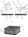
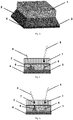
- the scintillator module comprises a pixellated scintillation array (1), a scintillator plate (2), and can also comprise an additional light guide (3).
- the whole assembly can be seen in Figures 2 and 3 , where also the incoming photons (5), preferably gamma photons, and the photodetector based on a SiPM array (4) are shown.
- Figure 9 shows a set of modules arranged on a ring forming a PET detector ring, also according to the first embodiment of the scintillator module.
- the example of the first preferred embodiment of the hybrid scintillation module as shown in Fig.
- the monolithic plate scintillator is also functioning as an active material detecting a fraction of the incoming radiation, preferably gamma radiation, that traversed the pixellated array without producing interactions.
- Figs. 10 and 11 show examples of operation of the embodiment from Fig.2 and 4 . They show the first reduction to practice of the first preferred embodiment using SensL SiPM array.
- images of the two components of the hybrid scintillator can be seen, both at 511 keV: 1.6mm pitch pixellated LYSO array coupled in front of the 12mm thick monolithic LYSO plate. 1.5mm pixels are seen well separated. At the bottom one can see only the image obtained at 511 keV from the pixellated component, plus the profile through one pixel row. Most pixels are shown well separated.
- the plot shows the raw image obtained at the energy of 511 keV, clearly indicating that the individual LYSO pixels are well separated in the image.
- an example of the individual energy spectrum obtained from one of the 1.5mm x 1.5mm x 10mm LYSO pixels is shown at right.
- the energy resolution of ⁇ 16% FWHM @ 511 keV is extracted from the data. While not yet optimized, the pilot results clearly demonstrate that the concept of the array-monolithic hybrid scintillator works.
- the pixellated scintillation array could be further vertically split into a stack of two or even more shifted arrays to improve DOI resolution of the detector module, as illustrated in Fig. 14 .
- the pixellated scintillation array as a stack of two shifted arrays on top of each other, typically both arrays will have the same pixel pitch and the shift is half a pitch in both X-Y planar coordinates.
Description
- Primarily this invention relates to the implementation of enhanced scintillation detectors in nuclear medicine imaging. It is specifically related to the special construction and method of coupling of scintillation crystals to photodetectors to provide highly accurate determination of the 3D conversion position of the impinging high energy radiation, preferably, gamma photons. Using this concept in Positron Emission Tomography (PET) imaging will result in high 3D spatial resolution tomographic system with high efficiency and moderate cost.
- However it is to be understood that the present invention is also applicable in many other technical fields, as for example in astrophysics, radiation safety or homeland security.
- A wide range of technical solutions was proposed in the past for achieving high three-dimensional spatial resolution in imaging radiation detectors, preferably gamma detectors, while assuring high detection efficiency. Achieving high resolution in Single Photon Computerized Tomography (SPECT) when using pinhole collimators or in coincidence Positron Emission Tomography (PET) detectors, requires not only high standard resolution in the plane of the detector module but also accurate information on the depth-of-interaction (DOI) of the converting photons inside the active material such as crystal scintillator. Common aspect of these both situations (pinhole SPECT and PET) is that there are many inclined radiation trajectories involved and to achieve high resolution operation, the information on the third - depth - coordinate of the point inside the scintillator module where the radiation, preferably gamma ray, interacted/converted, is necessary. Many technical approaches were developed in the past to achieve high DOI resolution and are for example described in the referenced review papers [1-5]. In the current invention, we propose a hybrid scintillator configuration for the scintillation crystals forming the scintillation detection block.
- Most scintillating crystal blocks for high spatial resolution detectors, preferably gamma ray detectors, such as the ones used in small animal PET scanners, use a configuration based on crystal pixel arrays (for example Naviscan's breast PET imager, Siemens microPET and INVEON small animal scanners, LabPET small animal PET from TriFoil imaging, etc). A new recent design based on continuous (also known as monolithic) crystal slabs has also shown excellent position resolution (Oncovision's MAMMI PET breast imager and ALBIRA small animal PET imager, University of Washington research effort, and Delft University in Holland research project). However, both pixellated and monolithic configurations present important limitations for thick (around 15mm or more in the PET detector) crystal blocks, required for stopping (and hence detecting) with high efficiency the high energy annihilation 511keV photons emitted by the PET radioisotopes. Crystal pixel arrays do not offer DOI information and when the pixels are very thin and long they provide poor energy and timing resolution and are costly to manufacture. Monolithic crystal slabs show poor spatial resolution at the edges and near the entrance surface when using thick crystals.
- Therefore, there are important drawbacks in the current technology: to solve these problems, in particular the conflict between the thickness-dependent detection efficiency of the monolithic crystal and the poor energy and timing resolution of the crystal pixel arrays, in this invention, we propose a hybrid configuration in which the scintillation block is a hybrid scintillation module formed by a component (or multiple components) of crystal pixel arrays coupled to a component (or multiple components) of a continuous crystal slab (or several slabs). Such hybrid configuration overcomes the mentioned limitations by providing high stopping power (the stopping power can be defined as the probability for the incoming radiation to deposit most of its energy in the target material (dE/dx) with high 3D resolution of the conversion position of the radiation, preferably gamma ray, inside the whole crystal block, and with good energy and timing resolutions, at the same time.
- It is important to clarify that the term "hybrid detector" was also used in the past in other contexts. In an example of one such use of the term "hybrid" (
US6819738 : "Hybrid scintillator / photo sensor & direct conversion detector") it describes the combination of two or more different radiation detection modality systems into one combined CT system. Other examples are PET/CT or PET/MRI imager combinations where two modalities operate as one system. - Another use of the "hybrid" term is given to the radiation sensor that functions as two types of modalities, for example to detect gamma and X-ray radiation and produce emission (gamma) and transmission (X-ray) images with the same radiation sensor.
US-6946841-B2 discloses an apparatus for combined nuclear imaging and magnetic resonance imaging, and method thereof. A combined MR and nuclear imaging device comprising an MRI device and a nuclear imaging device, wherein the nuclear imaging device is capable of operating with the magnetic field of the MRI device or in a region where the magnitude of the magnetic field is lower. The combined system allows MRI examination and nuclear medicine examinations to be conducted quasi-simultaneously with no, or minimal, motion of the patient during the combined examination. The nuclear imaging device comprises nuclear detector modules capable of operating within a large magnetic field in the bore of the MRI scanner when the modules are oriented in the direction of the field, and are capable of operating in any direction when the magnitude of the field is below a certain threshold. - Other efforts listed below refer to the crystal treatment and coupling methods.
US-6713767-B2 : "Hybrid two-dimensional scintillator arrangement" describes a scintillator arrangement comprising: a plurality of detector strips comprising a plurality of scintillator slabs, the scintillator slabs being separated from one another by absorber layers; and a fitting form wherein at least two of said plurality of detector strips are arranged essentially parallel to one another in said fitting form and wherein the fitting form comprises transverse pieces and a frame, the transverse pieces being arranged essentially parallel to one another and being attached to opposite sides of the frame. In our invention there are not absorbers in between the scintillators: the light is transferred from one slab to another. That design is only addressing the issue of two dimensional and not three dimensional arrangement. The many slabs are vertical and in our case there are only two that are horizontal. The absorber layers disclosed inUS-6713767 introduce asymmetry in the transversal light propagation and would decrease the performance in case they would be used in our structure. Except for the name, these two structures are entirely different. -
US 3978336-A discloses a hybrid scintillation scanning apparatus" that comprises: a scintillation crystal bar of elongated form receiving the gamma radiation through a collimator and comprising a transparent upper face optically coupled by means of a light guide to a plurality of photomultipliers. The photomultipliers furnish their signals to an electronic combining circuit supplying, on one hand, an amplitude analyzer and, on the other hand, a computing circuit permitting the location of the scintillation along the axis of the bar. The scanning apparatus disclosed in this patent does not include a combination of scintillation modules: one continue scintillation module and one pixellated scintillation module as the present invention does. It is therefore a completely different object. -
US-7692156-B1 "Beam-oriented pixellated scintillators for radiation imaging" discloses a radiation detection device, comprising: a two-dimensional, beam-oriented pixellated scintillator, the scintillator having a first pixel having a first pixel axis and a second pixel having a second pixel axis, wherein the first and second axes are at an angle relative to each other, and wherein each axis is substantially parallel to a predetermined beam direction for illuminating the corresponding pixel. According to particular embodiments, the device ofUS-7692156-B1 the scintillator comprises inter-pixel grooves and the pixels have a two dimensional monolithic array. This is entirely different from the two component scintillation module of the present invention. We are not using inter-pixel groves. -
CN102707310 discloses a device wherein "the array scintillation crystals are formed by strip-type scintillation crystals arranged along the width and length directions, the array scintillation crystals and the continuous scintillation crystals are sequentially coupled along the height direction of the strip-type scintillation crystals to form the multilayer scintillation crystal (1)". - The expressions "monolithic crystals", "monolithic scintillation slab", "monolithic scintillation plate", "continuous crystal slab", "continuous scintillation plate", "continuous scintillator plate" and monolithic scintillator are used indistinctly along this specification. The expressions "pixellated scintillator array", "pixellated scintillation array", and "pìxelated scintillation plate" are used interchangeably.
- In this application the expression "scintillation module", "scintillator module", and "scintillation block" are used interchangeably.
- The objective technical problem to be solved is to provide an efficient method to build high resolution scintillation modules that also provide high stopping power to the incoming radiation, preferably gamma radiation, and to achieve it in an economical manner.
- This invention describes an apparatus to detect radiation, preferably gamma rays, based on a hybrid scintillation module or block composed of a combination of continuous (also referred as monolithic) scintillator plate(s) and pixellated scintillator array(s) coupled to a photodetector.
- The method of coupling the two scintillator module components produces several important advantages when properly executed.
- The present invention therefore refers to a hybrid scintillation module for the detection of radiation according to
claim 1. - The present invention also refers to a hybrid scintillation device that according to
claim 9 comprises a hybrid scintillation module as defined inclaim 1 and at least a photodetector. Further advantages are contemplated in the dependent claims. - A practical example of such a hybrid structure is a 10mm thick LYSO (cerium-doped lutetium yttrium orthosilicate) plate coupled to a matching size array of 1.5
mm pitch 10 mm long LYSO pixels, subsequently coupled through a spreader light guide/window to an array of 3mm Silicon Photomultiplier sensors (SiPMs) distributed with a 3.1-4.0 mm pitch. - For any embodiment of the hybrid scintillation module of the invention the monolithic scintillation plate may be split into at least two stacked layers.
- Additional particular embodiments refer to a hybrid scintillation module comprising pixellated scintillation arrays arranged as a stack of at least two shifted arrays on top of each other.
- For any embodiment of the hybrid scintillation module of the invention the two (or more) scintillation components - the monolithic scintillation plate(s) and the pixellated scintillation array(s) - can be made of the same scintillation material or can be made of different scintillation materials. For instance LYSO or GSO (gadolinium orthosilicate (Gd2SiO5:Ce) or BGO (bismuth germinate Bi4Ge3O12) could be used. In the case of different scintillation materials care must be taken to assure that the materials placed between the top scintillator components and the photodetector do not absorb the scintillation light from the top layer. As well the light guide and optical coupling compounds, such as acrylic or glass plates with thicknesses varying from 0.1 to 10 mm, must be transmitting the scintillation light to the photodetector without significant losses. Preferred range for the window thickness is 1-4 mm.
- When the monolithic scintillation plate(s) and the pixellated scintillation array(s) are made of different scintillation materials they may have different light time properties (rise time and/or fall/decay time constants of their scintillators). This feature, if the rise time and/or decay times differences for the scintillation materials are large enough, can provide another complementary method to distinguish the two scintillator components. Additional readout electronics channels may be necessary to provide this additional analysis of the time shape of the scintillation pulses.
- The hybrid scintillation module of the invention can further comprise hardware and software means for extracting 3D information on the position of the radiation, preferably gamma, conversion event from the planar 2D distribution of the scintillation light cone at the photodetector surface. Said means are in a particular embodiment a 3D spatial calculation algorithm that extracts the 3D information on the position of the radiation, preferably gamma, conversion event from the planar 2D distribution of the scintillation light cone at the photodetector surface. The set of individual readout channels from the photodetector measures the scintillation light distribution emerging from the scintillation module and based on this calculates the position in 3D of the scintillation light source inside the scintillation module. The software algorithm employs mathematical analysis of the measured light distribution to extract the originating position of the scintillation light. There are different algorithms that can be implemented but the preferred one is the one using the physical modelling (simulation) of the scintillation light generation and progression through the scintillation module on the way to the photodetector, and comparing the simulation results with the actual experimentally measured spatial distribution. After the repeated (iterative) simulation, the results converge with the experimental distribution, and the calculated or estimated position in 3D is extracted from the best fit. This calculation is done on the scintillation detected photons on an event by event basis. It requires very fast computing system. The method works best for the monolithic plates because monolithic scintillators inherently provide information of the 3-D impact coordinates of the photon interactions. The detected light is fitted to a theoretical expression based on the optics of scintillation light propagation in the scintillator. An example of algorithm is an optimization of the Levenberg-Marquardt method implemented in the open source numerical analysis and data processing library ALGLIB (www.alglib.net).
- According to particular embodiments of the hybrid scintillation module, it comprises a pixellated scintillation array in front of a monolithic scintillation plate, wherein the thickness of the pixellated scintillation array is lower than the thickness of the monolithic scintillation plate. In other word, the hybrid module of the invention may use the dual "high resolution/full resolution" concept by utilizing thin pixellated array in front of the thicker plate scintillator. In this way three images are produced: high resolution part of the imager only that produces a high resolution image, moderate resolution part of the imager only producing a moderate resolution image, and finally the full system resolution by combining the two above mentioned parts of the detector and producing a full resolution image.
- The hybrid scintillation device of the invention can further comprise a fiberoptic light guide inserted in front of the photodetector to transport light further away from the scintillator before coupling it to the photodetector.
- According to additional particular embodiments or the hybrid scintillation module, it can further comprise an optically transmitting radiofrequency (RF) shield layer, or layers, inserted between the fiberoptic lightguide and the scintillator module to improve the RF shielding between the detector modules and the MRI scanner RF fields due to its electromagnetic properties, making the modules MR-compatible and allowing the construction of the PET/MR (Positron Emission Tomography (PET) / Magnetic Resonance) dual-modality imager.
- The pixellated scintillation arrays need proper surface treatments to operate in an optimal way. The surface treatment of the scintillators and especially of the pixellated scintillation array needs to be optimized as it has large effect on the scintillation module performance. A very important and non-standard novel concept disclosed here and demonstrated already in the "reduction to practice" comparative experiments, is that when the side surfaces of the scintillation pixels in the pixellated scintillation array are rough-cut ("as-cut") and not polished, especially when scintillation array is placed on top of the monolithic scintillation plate, the detector operation is better: higher detected scintillation signal and better scintillation pixel separation in the images. The explanation is that the scintillation light cone exiting from the pixels and then propagating across the monolithic scintillator gap on a way to the photodetector is wider for the "as-cut" side surface treatment as compared to the polished surface treatment The cone opening angle is made wider when the scintillation photon bunch is propagating through the scintillation pixel and bouncing multiple times off the pixel side walls with rougher treatment as scintillation photons undergo wider angle scattering, while in the polished pixel case the photon propagation is governed by the total internal light reflection process, producing narrower and defined by the refractive index angle limits. Wider cone produces larger scintillation light imprint on the surface of the photodetector and subsequently allows for finer scintillation light signal sampling with the fixed-pitch photodetector and as a result produces better definition of the centre of gravity of the light distribution. By this, the achieved separation of the scintillation pixels is greatly improved in the rough surface treatment case. In fact our experimental evidence is that while in some tested cases where the only difference was the side surface treatment (same pixel pitch and size, same lightguide, same photodetector, etc) the standard polished variant provided poor pixel separation while with the "as-cut" variant the pixel separation as well as energy resolution were excellent.
- Preferred embodiments are disclosed in the dependent claims. Some of these claims cover the particular conditions that need to be met for the hybrid scintillator concept to operate optimally.
- The invention has the following key advantages:
- allows application of two and more scintillation components and increasing stopping power and detection efficiency of the whole module, while not decreasing spatial resolution; the individual components have typical thicknesses of 5-15mm each (in the case of the LYSO scintillator); in a typical arrangement, preferred also from the cost point of view, both components will be 10mm thick.
- enables a "high resolution/full resolution" dual operation mode approach through application of thinner (app. <=5mm) pixellated front component that provides very high upfront 2D spatial resolution performance, for a substantial fraction (30-60%) of the total detected annihilation photons by the module; using only this detector component will produce separate high resolution images albeit with lower efficiency,
- to improve DOI resolution of the pixellated component it can be split into two or more sub-layers and separated on the basis of relative spatial (x-y) shifts and/or by scintillation light characteristics (for example by using two or more different scintillator materials with different time shapes of the scintillation pulses that can be recorded),
- the monolithic component will provide additional stopping power with a coarser but sufficient 2D spatial resolution and with good Depth-of-Interaction (DOI) resolution;
- using additive image processing algorithm, a combination of the previously obtained high resolution images and of the moderate resolution images coming from the coarser resolution component of the detector will produce full efficiency images, however with the high resolution component of the reconstructed images dominating detection of the hot features, such as small structures or lesions. The added system sensitivity due to the additional stopping power of the second scintillation component albeit with lower spatial resolution - is increasing the statistical strength of the detected signal in the form of increased Signal-to-Noise (S/N) ratio and higher "contrast values". Contrast is defined as the relative difference in counts per image pixel or difference in intensity between two points in an image. ·"Contrast resolution" is defined as the ability to distinguish between areas in an image (such as different tissues) due to the difference in count densities of the two areas.
- A hybrid scintillation module according to the invention has the following key advantages:
- allows application of the economical yet high performing monolithic component having optimal thickness (on the order of 50% of the total thickness), while increasing stopping power of the whole module,
- through application of the monolithic front component it provides high upfront 3D spatial resolution performance, including DOI, for the major fraction of the detected events by the imager,
- the pixellated second component placed behind the monolithic component provides additional stopping power with high 2D spatial resolution and coarser but sufficient in many imaging tasks DOI resolution;
- to improve DOI resolution of the pixellated component is split into two or more sub-layers and separated on the basis of relative spatial (x-y) shifts and/or by scintillation light characteristics (for example by using two or more different scintillator materials).
- An advantage of the hybrid scintillation module of the present invention is that it improves the spatial resolution and response uniformity across the whole detector module, and especially in the edge regions, while maintaining high efficiency and energy resolution across the module.
- The present invention further refers to the use of the hybrid scintillation module defined herein or the device comprising said hybrid scintillation module in nuclear medicine imaging, preferably Single-Photon Emission Computed Tomography, SPECT, or Positron Emission Tomography, PET.
-
-
Fig.1 : Concept of the Depth-of-Interaction (DOI) 10 in two generic examples of radiation, preferably gamma, detection modules. Radiation, preferably gamma rays, 5 typically arrive at some angle and interact at the different depths. Light from scintillation modules 1-2 is detected inphotodetectors 4. Example of the first preferred embodiment with the pixellated scintillation array(s) placed upfront facing the incident ray, preferably gamma ray beam, and, thus, on top of the monolithic plate(s) with the photodetector on the other side of the monolithic plate and receiving scintillation light from both components of the scintillator module.
Readout for one component (left) and two-component (right) scintillation module. -
Fig. 2 : Particular example of the first embodiment: a pixellated scintillation component in front (1), is followed by the monolithic scintillation component (2), the spreader window or light guide (3) and the photodetector (4). -
Fig. 3 : A variant of the first preferred embodiment of the hybrid scintillator module with a tapered monolithic scintillator. -
Fig. 4 : Simplified representation of scintillation light propagation (6) in the first embodiment with radiation, preferably gamma rays (5) converting in both scintillator components. -
Fig. 5 : Sketch of scintillation light propagation mechanism's; in the rough surface pixels (7) it produces wider opening angle scintillation light cone entering into the monolithic scintillator component where it propagates with the same angle opening (in the case of the same scintillator material in both components) until it reaches the multi-element photodetector. The light cone with a larger imprint on the photodetector produces more precise (less image non-uniformity) definition of the centre of gravity of the scintillation light spot and by this it provides better separation of the detection events produced in the neighbouring scintillation pixels. -
Fig. 6 : shows a particular example in which the pixellated scintillator array is split into two stacked layers, (1) and (8). -
Fig. 7 : shows a fiberoptic lightguide (9) that can be used between the scintillator module and the photodetector in some situations requiring stand-off distance between the scintillator and electronics (to minimize mechanical edge effects or to avoid electromagnetic interference). -
Fig. 8 : shows modules arranged in a PET detector ring according to the first embodiment of the scintillation module. -
Fig. 9 : shows the tapered shape of the monolithic section fromFig. 3 and how it enables higher packing fraction of the modules placed on a ring and how it minimizes the physical gaps between the modules. -
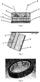
Fig. 10 : shows the first reduction to practice of the first preferred embodiment using SensL (Cork, Ireland) Silicon Photomultiplier (SiPM) array. The monolithic in between the crystal array and the photodetector has 12mm thickness. Top: Sketch, 2D contour plot of the crystal array at 511 keV where most pixels of 2 mm size are shown well separated, and energy spectrum showing both monolithic and pixellated contributions. Bottom: Profiles of one row and one column of the pixellated contribution. -
Fig. 11 : First reduction to practice as inFigure 13 but using 1.5mm x 1.5mm crystal pixels. -
Fig. 12 : Demonstration of the importance of surface treatment of the pixellated component of the hybrid scintillator module with the pixellated scintillation array being on top of the monolithic scintillation plate. From two otherwise identical 10x10 LYSO arrays of 1.5x1.5x10mm pixels from Proteus, one had side walls of the "as-cut" quality, while the second had all sides polished. The one with "as-cut" surfaces had about factor two higher signal response in the MPPC (Multi-Pixel Photon Counter) photodetector and the individual pixels were distinguished in the raw image (center) while in the all-sides-polished case the pixels were not separated (right) even at a higher energy of 1274 keV. In this measurement the LYSO plate of 12 mm was used demonstrating the limitation of the hybrid approach with greater scintillator thickness. (Measurement was performed at temperature of 22 degrees C). -
Fig. 13 . Generic drawing of a ring of modules showing scintillation blocks A (one or many layers) coupled to the photodetector modules with electronics B, through the fiberoptic light guides C. The fiberoptic light guides built from arranged arrays of fibers or individual optical channels are image-preserving and their purpose is to transport in parallel fashion scintillation light as it is emerging from the scintillation module, to the photodetector placed at the other end of the light guide. Implementation of the fiberoptic light guide provides stand-off distance between the scintillator modules and the photodetector modules and in typical situations will minimize the dead regions - breaks between the scintillation modules. Considering the application of the PET insert in MRI, a relatively thin additional optical window may be inserted between the scintillator and the fiberoptic lightguide, that can also serve as a component of the RF shield D between the photodetector/electronics modules and the RF field of the MRI. This window will be based on special materials that provide RF shield and are optically transparent to the scintillation light. -
Figure 14 shows an example of a scintillator module structure with thepixellated array 1 split into two pixellated arrays placed on top of each other and shifted sideways, and then coupled to themonolithic scintillator plate 2. Scintillation light from the top pixellated array propagates into bottom pixellated array and then continues into thescintillation plate 2 and to thephotodetector 4 vialightguide 3. Thescintillation light cones 6 from the two sub-arrays are shifted relatively to each other at the photodetector surface and this allows to differentiate the gamma interactions in the top array from the interactions in the bottom array. -
- 1) Pixel crystal array. A pixel crystal array is a scintillation block made out of many small crystal scintillation crystals-elements, merged (glued) together, typically with all walls and faces polished. The dimensions of each crystal pixel will depend on the resolution goal. The outer dimensions of the pixel array will depend on the selected configuration and system geometry.
- 2) Monolithic crystal. This is a single, continuous, block of scintillation material. As shown in
Figure 4 the shape of this crystal can vary depending on the chosen configuration. Rectangular and trapezoidal shapes are the most suggested, but others could also be possible. - 3) Spreader window or light guide. Spreader windows are typically made out of acrylic or glass material. Their thickness can vary from few tenths of a millimetre to few millimeters.
- 4) Photodetector. Several types of photodetectors can be employed, such as position sensitive photomultipliers (PSPMTs), photodiodes with and without gain (avalanche photodiodes, APDs), and silicon photomultipliers (SiPMs). Their common feature is that they are position sensitive and provide spatial information on the scintillation light distribution. The preferred option for the photodetector for our concept is array of Silicon Photomultipliers (SiPMs).
- 5) Impinging rays, preferably gamma rays. The photons, preferably gamma photons, are emitted by the objects that were injected or otherwise inserted mechanically or chemically with the radioactive compounds. In the case of Positron Emission Tomography (PET) typically the positron emitting radolabeled compounds are injected in patients and the emitted annihilation 511 keV photons are emitted from the uptake sites in the patient body. The purpose of the detector modules is to stop and detect these photons, preferably gamma photons. Annihilation photons can come (impinge) at different angles to the front of the detector module. Typically the angle range is within +/- 45 deg measured from the vertical to the detector module.
- 6) Scintillation light distribution, light cones. The scintillation light comes out of the scintillator in a cone-like shape, more regular in the scintillator centre and distorted - compressed at the edges. Measurement of this light distribution to back-calculate the original conversion point of the impinging photon inside the scintillation module is the main purpose of the photodetector and the associated electronics.
- 7) Pixel crystal where the lateral faces are "as-cut" in contrast to polished.
- 8) Pixel crystal array with different scintillation material compared to (1).
- 9) Additional light guide, such as fiberoptic light guide to transport light further away from the scintillator module to minimize edge effects or remove photodetector with front-end electronics further from the object and for example out of the central MRI magnetic and radiofrequency field.
- According to the first embodiment, the scintillator module comprises a pixellated scintillation array (1), a scintillator plate (2), and can also comprise an additional light guide (3). The whole assembly can be seen in
Figures 2 and3 , where also the incoming photons (5), preferably gamma photons, and the photodetector based on a SiPM array (4) are shown.Figure 9 shows a set of modules arranged on a ring forming a PET detector ring, also according to the first embodiment of the scintillator module. According to the example of the first preferred embodiment of the hybrid scintillation module as shown inFig. 2 and4 , there is a pixellated array on top of the monolithic scintillator. The scintillation light from the array on its way to the photodetector passes through the monolithic crystal acting here as an optical window. At the same time, the monolithic plate scintillator is also functioning as an active material detecting a fraction of the incoming radiation, preferably gamma radiation, that traversed the pixellated array without producing interactions. - Small LYSO array of 1.5mm step and 10mm long pixels was placed on top of a 10mm thick monolithic plate of LYSO scintillator. On the other side of the monolithic plate a Silicon Photomultiplier photodetector was placed composed of a 4x4 array of 3mm MPPC sensors from Hamamatsu. Na22 source of annihilation 511 keV photons (and 1274 keV gammas) was placed above the LYSO array.
-
Figs. 10 and11 show examples of operation of the embodiment fromFig.2 and4 . They show the first reduction to practice of the first preferred embodiment using SensL SiPM array. At the top raw, images of the two components of the hybrid scintillator can be seen, both at 511 keV: 1.6mm pitch pixellated LYSO array coupled in front of the 12mm thick monolithic LYSO plate. 1.5mm pixels are seen well separated. At the bottom one can see only the image obtained at 511 keV from the pixellated component, plus the profile through one pixel row. Most pixels are shown well separated. - The plot shows the raw image obtained at the energy of 511 keV, clearly indicating that the individual LYSO pixels are well separated in the image. In addition, an example of the individual energy spectrum obtained from one of the 1.5mm x 1.5mm x 10mm LYSO pixels is shown at right. After correcting for the energy non-linearity present when using the special diode based 4ch charge division readout (from AiT Instruments), the energy resolution of ∼16% FWHM @ 511 keV is extracted from the data. While not yet optimized, the pilot results clearly demonstrate that the concept of the array-monolithic hybrid scintillator works.
- The pixellated scintillation array could be further vertically split into a stack of two or even more shifted arrays to improve DOI resolution of the detector module, as illustrated in
Fig. 14 . With the pixellated scintillation array as a stack of two shifted arrays on top of each other, typically both arrays will have the same pixel pitch and the shift is half a pitch in both X-Y planar coordinates. -
- 1. Mikiko Ito, Seong Jong Hong and Jae Sung Lee, Positron Emission Tomography (PET) Detectors with Depth-of- Interaction (DOI) Capability, Biomed Eng Lett (2011) 1:70-81. DOI 10.1007/s13534-011-0019-6
- 2. Jae Sung Lee, Technical Advances in Current PET and Hybrid Imaging Systems, The Open Nuclear Medicine Journal, 2010, 2, 192-20.
- 3. Thomas K. Lewellen, The Challenge of Detector Designs for PET, AJR 2010; 195:301-309.
- 4. Hao Peng and Craig S. Levin, Recent Developments in PET Instrumentation, Current Pharmaceutical Biotechnology, 2010, 11, 555-571.
- 5. Craig S. Levin, New Imaging Technologies to Enhance the Molecular Sensitivity of Positron Emission Tomography, Proceedings of the IEEE, Vol. 96, No. 3, March 2008, 439-467.
Claims (14)
- A hybrid scintillation module for the detection of radiation, comprising a combination of:- pixellated scintillation arrays (1)- at least a first monolithic scintillation plate (2), that has a trapezoidal shapewherein the pixellated scintillation arrays (1) are at the front of the hybrid scintillation module and the monolithic plate (2) is behind the pixellated scintillation arrays (1),
characterized in that
the pixellated scintillator arrays (1) are arranged as a stack of at least two shifted arrays. - A hybrid scintillation module according to claim 1 , characterized in that the monolithic scintillation plate (2) is split into at least two stacked layers (8).
- A hybrid scintillation module according to any of the preceding claims, characterized in that it further comprises at least a light spreader window.
- A hybrid scintillation module according to any of the preceding claims, characterized in that it further comprises at least a refractive optical coupling compound which has a refractive index n, within the range 1.4<n<1.8.
- A hybrid scintillation module according to any of the preceding claims, characterized in that the monolithic scintillation plate (2) and the pixellated scintillation array are made of the same scintillation material or of different scintillation materials.
- A hybrid scintillation module, according to claim 1 wherein the thickness of the pixellated scintillation arrays (1) is lower than the thickness of the monolithic scintillation plate (2).
- A hybrid scintillation module according to claim 1 characterized in that the pixellated scintillation arrays (1) are arranged as a stack of at least two shifted arrays on top of each other.
- A hybrid scintillation module according to claim 1, characterized in that the scintillation array is rough-cut and not polished.
- A hybrid scintillation device, characterized in that it comprises a hybrid scintillation module defined in any of claims 1 to 8 and at least a photodetector (4).
- A hybrid scintillation device according to claim 9, further comprising means for extracting 3D information on the position of the radiation conversion event from the planar 2D distribution of the scintillation light cone at the photodetector surface.
- A hybrid scintillation device according claim 10 wherein said means are a 3D spatial differentiation algorithm for extracting the 3D information on the position of the radiation conversion event from the planar 2D distribution of the scintillation light cone at the photodetector surface.
- A hybrid scintillation module according to any of the preceding claims 1 to 8, or a hybrid scintillation device, according to any of the preceding claims 9 to 11, characterized in that the radiation is gamma radiation.
- A hybrid scintillation device, according to any of claims 9 to 12 that further comprises fiberoptic lightguide (9) between the hybrid scintillation module and the photodetector (4) to transport light further away from the scintillator sensor.
- Use of the hybrid scintillation module defined in any of claims 1 to 8 or the device defined in claim 9 to 13 in nuclear medicine imaging, preferably Single-Photon Emission Computed Tomography, SPECT, or Positron Emission Tomography, PET.
Priority Applications (5)
| Application Number | Priority Date | Filing Date | Title |
|---|---|---|---|
| ES14382440T ES2743542T3 (en) | 2014-11-06 | 2014-11-06 | Hybrid Scintillation Module |
| EP14382440.7A EP3018496B1 (en) | 2014-11-06 | 2014-11-06 | Hybrid scintillation module |
| JP2017524467A JP6670307B2 (en) | 2014-11-06 | 2015-11-06 | Hybrid scintillation module |
| PCT/EP2015/075916 WO2016071494A1 (en) | 2014-11-06 | 2015-11-06 | Hybrid scintillation module |
| US15/586,908 US10228471B2 (en) | 2014-11-06 | 2017-05-04 | Hybrid scintillation module |
Applications Claiming Priority (1)
| Application Number | Priority Date | Filing Date | Title |
|---|---|---|---|
| EP14382440.7A EP3018496B1 (en) | 2014-11-06 | 2014-11-06 | Hybrid scintillation module |
Publications (2)
| Publication Number | Publication Date |
|---|---|
| EP3018496A1 EP3018496A1 (en) | 2016-05-11 |
| EP3018496B1 true EP3018496B1 (en) | 2019-06-05 |
Family
ID=51893961
Family Applications (1)
| Application Number | Title | Priority Date | Filing Date |
|---|---|---|---|
| EP14382440.7A Active EP3018496B1 (en) | 2014-11-06 | 2014-11-06 | Hybrid scintillation module |
Country Status (5)
| Country | Link |
|---|---|
| US (1) | US10228471B2 (en) |
| EP (1) | EP3018496B1 (en) |
| JP (1) | JP6670307B2 (en) |
| ES (1) | ES2743542T3 (en) |
| WO (1) | WO2016071494A1 (en) |
Families Citing this family (10)
| Publication number | Priority date | Publication date | Assignee | Title |
|---|---|---|---|---|
| KR101882351B1 (en) * | 2017-01-02 | 2018-07-26 | 서강대학교산학협력단 | Hybrid scintillator for radiation imaging device |
| JP2020529607A (en) | 2017-08-03 | 2020-10-08 | ザ・リサーチ・ファウンデーション・フォー・ザ・ステイト・ユニヴァーシティ・オブ・ニューヨーク | Dual screen digital radiation imaging with asymmetric reflective screen |
| EP3495849A1 (en) * | 2017-12-11 | 2019-06-12 | Koninklijke Philips N.V. | Multilayer pixelated scintillator with enlarged fill factor |
| KR20230110665A (en) * | 2018-04-02 | 2023-07-24 | 에이에스엠엘 네델란즈 비.브이. | Architecture for large active area high speed detector |
| IT201900000076A1 (en) * | 2019-01-04 | 2020-07-04 | Univ Degli Studi Padova | DEVICE AND PROCEDURE FOR MEASURING THE WATER CONTENT OF THE SOIL, VEGETATION AND SNOW COVER |
| WO2020208203A1 (en) * | 2019-04-12 | 2020-10-15 | Arktis Radiation Detectors Ltd. | Panel radiation detector |
| CN111025370A (en) * | 2019-12-10 | 2020-04-17 | 南昌大学 | Radiation sensing device made of two-state functional material and assembling method thereof |
| ES2847577A1 (en) * | 2020-02-03 | 2021-08-03 | Univ Valencia Politecnica | DEVICE FOR DETECTION OF GAMMA RAYS BASED ON BLOCKS OF METACENTELLEO DETECTION (Machine-translation by Google Translate, not legally binding) |
| US20220120921A1 (en) * | 2020-10-16 | 2022-04-21 | Brown Universtiy | High resolution x-ray detector system |
| WO2023244268A1 (en) * | 2022-06-14 | 2023-12-21 | Siemens Medical Solutions Usa, Inc. | Emission tomography with generalized time encoded aperture imaging |
Family Cites Families (22)
| Publication number | Priority date | Publication date | Assignee | Title |
|---|---|---|---|---|
| FR2323158A1 (en) | 1974-01-10 | 1977-04-01 | Radiologie Cie Gle | HYBRID SCAN SCINTIGRAPHY UNIT |
| JPH0961533A (en) * | 1995-08-25 | 1997-03-07 | Hamamatsu Photonics Kk | Scintillator and scintillation detector |
| US5652429A (en) * | 1995-10-19 | 1997-07-29 | Digital Scintigraphics, Inc. | Liquid interface scintillation camera |
| DE10121018A1 (en) | 2001-04-28 | 2002-10-31 | Philips Corp Intellectual Pty | Hybrid 2D scintillator arrangement has detector strips arranged parallel with each other in defined shape consisting of frame with mutually parallel bridges joined to ends of frame |
| JP2003021682A (en) * | 2001-07-09 | 2003-01-24 | Natl Inst Of Radiological Sciences | Radiation three-dimensional position detector |
| US6946841B2 (en) | 2001-08-17 | 2005-09-20 | Igor Rubashov | Apparatus for combined nuclear imaging and magnetic resonance imaging, and method thereof |
| US6819738B2 (en) | 2002-08-15 | 2004-11-16 | Ge Medical Systems Global Technology Company, Llc | Hybrid scintillator/photo sensor & direct conversion detector |
| JP2004125722A (en) * | 2002-10-07 | 2004-04-22 | Hitachi Medical Corp | Radiation detector and x-ray ct system using it |
| JP2007514143A (en) * | 2003-11-25 | 2007-05-31 | コーニンクレッカ フィリップス エレクトロニクス エヌ ヴィ | Scintillation layer for PET detector |
| WO2006107727A2 (en) * | 2005-04-01 | 2006-10-12 | San Diego State University Foundation | Edge-on sar scintillator devices and systems for enhanced spect, pet, and compton gamma cameras |
| US7692156B1 (en) | 2006-08-23 | 2010-04-06 | Radiation Monitoring Devices, Inc. | Beam-oriented pixellated scintillators for radiation imaging |
| AU2008204559A1 (en) * | 2007-01-10 | 2008-07-17 | Tomtom International B.V. | Navigation device and method |
| US8008542B2 (en) * | 2007-01-10 | 2011-08-30 | The Salk Institute For Biological Studies | Compositions, cells, and plants that include BKI1, a negative regulator of BRI1-mediated BR signaling |
| US8183531B2 (en) * | 2007-05-21 | 2012-05-22 | The Board Of Trustees Of The Leland Stanford Junior University | System and method for tomography combining single and paired photons |
| US9497419B2 (en) * | 2007-06-27 | 2016-11-15 | Arris Enterprises, Inc. | Method and apparatus for delivering programming code objects to set-top terminals and the like |
| JP5595082B2 (en) * | 2010-03-29 | 2014-09-24 | キヤノン株式会社 | Novel benzoxazolylcarbazole compound and organic light emitting device having the same |
| JP2013019796A (en) * | 2011-07-12 | 2013-01-31 | Canon Inc | Radiation detector |
| CN102707310B (en) * | 2012-06-21 | 2014-06-11 | 苏州瑞派宁科技有限公司 | Positron emission tomography detector for multilayer scintillation crystal |
| WO2014052029A1 (en) * | 2012-09-30 | 2014-04-03 | Saint-Gobain Ceramics & Plastics, Inc. | Scintillation pixel array, radiation sensing apparatus including the scintillation pixel array and a method of forming a scintillation pixel array |
| JP6057207B2 (en) * | 2012-10-02 | 2017-01-11 | 国立大学法人名古屋大学 | Radiation position detector |
| KR101542836B1 (en) * | 2013-05-27 | 2015-08-10 | 서강대학교산학협력단 | Detector for Positron Emission Tomography and Positron Emission Tomography system using the same |
| WO2016015061A1 (en) * | 2014-07-25 | 2016-01-28 | The Regents Of The University Of California | Multiple spatial resolution scintillation detectors |
-
2014
- 2014-11-06 ES ES14382440T patent/ES2743542T3/en active Active
- 2014-11-06 EP EP14382440.7A patent/EP3018496B1/en active Active
-
2015
- 2015-11-06 WO PCT/EP2015/075916 patent/WO2016071494A1/en active Application Filing
- 2015-11-06 JP JP2017524467A patent/JP6670307B2/en active Active
-
2017
- 2017-05-04 US US15/586,908 patent/US10228471B2/en active Active
Non-Patent Citations (1)
| Title |
|---|
| ZHANG H ET AL: "Performance Characteristics of BGO Detectors for a Low Cost Preclinical PET Scanner", IEEE TRANSACTIONS ON NUCLEAR SCIENCE, IEEE SERVICE CENTER, NEW YORK, NY, US, vol. 57, no. 3, 1 June 2010 (2010-06-01), pages 1038 - 1044, XP011311667, ISSN: 0018-9499 * |
Also Published As
| Publication number | Publication date |
|---|---|
| ES2743542T3 (en) | 2020-02-19 |
| US20170234991A1 (en) | 2017-08-17 |
| JP2018500545A (en) | 2018-01-11 |
| JP6670307B2 (en) | 2020-03-18 |
| WO2016071494A1 (en) | 2016-05-12 |
| US10228471B2 (en) | 2019-03-12 |
| EP3018496A1 (en) | 2016-05-11 |
Similar Documents
| Publication | Publication Date | Title |
|---|---|---|
| US10228471B2 (en) | Hybrid scintillation module | |
| US9442198B2 (en) | Optical-interface patterning for radiation detector crystals | |
| US9535169B2 (en) | Radiation detector | |
| US10281594B2 (en) | Gamma-ray Compton TOF camera system | |
| US11385362B2 (en) | Scintillation detector and associated scintillation detector ring and method | |
| US7635848B2 (en) | Edge-on SAR scintillator devices and systems for enhanced SPECT, PET, and compton gamma cameras | |
| US9442199B2 (en) | Depth-of-interaction scintillation detectors | |
| US20100012846A1 (en) | Novel scintillation detector array and associate signal processing method for gamma ray detection with encoding the energy, position, and time coordinaties of the interaction | |
| EP3210042B1 (en) | Detector component for an x-ray or gamma ray detector | |
| US9304211B2 (en) | Scintillation detector with active light guide | |
| US8063377B2 (en) | Crystal identification for high resolution nuclear imaging | |
| US20030193029A1 (en) | Edge resolved dual scintillator gamma ray detection system and method | |
| EP2536337A1 (en) | A method and system for nuclear imaging using multi-zone detector architecture | |
| US11819346B2 (en) | Scintillation detector based systems and methods for using the same | |
| EP3908856A1 (en) | Prismatoid light guide | |
| US9612344B2 (en) | Positron emission tomography and single photon emission computed tomography based on intensity attenuation shadowing methods and effects | |
| Zaidi et al. | The new challenges of brain PET imaging technology | |
| WO2020013689A1 (en) | Active collimator system comprising a monolayer of monolithic converters | |
| WO2016112135A1 (en) | Compact trapezoidal pet detector with light sharing | |
| Benlloch Baviera et al. | Hybrid scintillation module | |
| EP4095565A1 (en) | Device for the detection of gamma rays with interaction depth and time-of-flight encoding | |
| Andreas | Novel High Resolution Photon Detectors for PET Imaging |
Legal Events
| Date | Code | Title | Description |
|---|---|---|---|
| PUAI | Public reference made under article 153(3) epc to a published international application that has entered the european phase |
Free format text: ORIGINAL CODE: 0009012 |
|
| AK | Designated contracting states |
Kind code of ref document: A1 Designated state(s): AL AT BE BG CH CY CZ DE DK EE ES FI FR GB GR HR HU IE IS IT LI LT LU LV MC MK MT NL NO PL PT RO RS SE SI SK SM TR |
|
| AX | Request for extension of the european patent |
Extension state: BA ME |
|
| STAA | Information on the status of an ep patent application or granted ep patent |
Free format text: STATUS: REQUEST FOR EXAMINATION WAS MADE |
|
| 17P | Request for examination filed |
Effective date: 20161109 |
|
| RBV | Designated contracting states (corrected) |
Designated state(s): AL AT BE BG CH CY CZ DE DK EE ES FI FR GB GR HR HU IE IS IT LI LT LU LV MC MK MT NL NO PL PT RO RS SE SI SK SM TR |
|
| STAA | Information on the status of an ep patent application or granted ep patent |
Free format text: STATUS: EXAMINATION IS IN PROGRESS |
|
| RAP1 | Party data changed (applicant data changed or rights of an application transferred) |
Owner name: CONSEJO SUPERIOR DE INVESTIGACIONES CIENTIFICAS (C Owner name: UNIVERSITAT POLITECNICA DE VALENCIA Owner name: WEST VIRGINIA UNIVERSITY Owner name: GENERAL EQUIPMENT FOR MEDICAL IMAGING, S.A. |
|
| 17Q | First examination report despatched |
Effective date: 20180201 |
|
| REG | Reference to a national code |
Ref country code: DE Ref legal event code: R079 Ref document number: 602014047782 Country of ref document: DE Free format text: PREVIOUS MAIN CLASS: G01T0001164000 Ipc: G01T0001200000 |
|
| GRAP | Despatch of communication of intention to grant a patent |
Free format text: ORIGINAL CODE: EPIDOSNIGR1 |
|
| STAA | Information on the status of an ep patent application or granted ep patent |
Free format text: STATUS: GRANT OF PATENT IS INTENDED |
|
| RIC1 | Information provided on ipc code assigned before grant |
Ipc: G01T 1/20 20060101AFI20180925BHEP |
|
| INTG | Intention to grant announced |
Effective date: 20181030 |
|
| GRAS | Grant fee paid |
Free format text: ORIGINAL CODE: EPIDOSNIGR3 |
|
| RAP1 | Party data changed (applicant data changed or rights of an application transferred) |
Owner name: CONSEJO SUPERIOR DE INVESTIGACIONES CIENTIFICAS (C Owner name: UNIVERSITAT POLITECNICA DE VALENCIA Owner name: GENERAL EQUIPMENT FOR MEDICAL IMAGING, S.A. Owner name: WEST VIRGINIA UNIVERSITY |
|
| GRAA | (expected) grant |
Free format text: ORIGINAL CODE: 0009210 |
|
| STAA | Information on the status of an ep patent application or granted ep patent |
Free format text: STATUS: THE PATENT HAS BEEN GRANTED |
|
| AK | Designated contracting states |
Kind code of ref document: B1 Designated state(s): AL AT BE BG CH CY CZ DE DK EE ES FI FR GB GR HR HU IE IS IT LI LT LU LV MC MK MT NL NO PL PT RO RS SE SI SK SM TR |
|
| RAP1 | Party data changed (applicant data changed or rights of an application transferred) |
Owner name: GENERAL EQUIPMENT FOR MEDICAL IMAGING, S.A. Owner name: UNIVERSITAT POLITECNICA DE VALENCIA Owner name: CONSEJO SUPERIOR DE INVESTIGACIONES CIENTIFICAS (C Owner name: WEST VIRGINIA UNIVERSITY Owner name: BRUKER BIOSPIN AG |
|
| REG | Reference to a national code |
Ref country code: GB Ref legal event code: FG4D |
|
| REG | Reference to a national code |
Ref country code: CH Ref legal event code: EP |
|
| REG | Reference to a national code |
Ref country code: AT Ref legal event code: REF Ref document number: 1140571 Country of ref document: AT Kind code of ref document: T Effective date: 20190615 |
|
| REG | Reference to a national code |
Ref country code: DE Ref legal event code: R096 Ref document number: 602014047782 Country of ref document: DE |
|
| REG | Reference to a national code |
Ref country code: IE Ref legal event code: FG4D |
|
| REG | Reference to a national code |
Ref country code: NL Ref legal event code: MP Effective date: 20190605 |
|
| REG | Reference to a national code |
Ref country code: LT Ref legal event code: MG4D |
|
| PG25 | Lapsed in a contracting state [announced via postgrant information from national office to epo] |
Ref country code: SE Free format text: LAPSE BECAUSE OF FAILURE TO SUBMIT A TRANSLATION OF THE DESCRIPTION OR TO PAY THE FEE WITHIN THE PRESCRIBED TIME-LIMIT Effective date: 20190605 Ref country code: LT Free format text: LAPSE BECAUSE OF FAILURE TO SUBMIT A TRANSLATION OF THE DESCRIPTION OR TO PAY THE FEE WITHIN THE PRESCRIBED TIME-LIMIT Effective date: 20190605 Ref country code: AL Free format text: LAPSE BECAUSE OF FAILURE TO SUBMIT A TRANSLATION OF THE DESCRIPTION OR TO PAY THE FEE WITHIN THE PRESCRIBED TIME-LIMIT Effective date: 20190605 Ref country code: NO Free format text: LAPSE BECAUSE OF FAILURE TO SUBMIT A TRANSLATION OF THE DESCRIPTION OR TO PAY THE FEE WITHIN THE PRESCRIBED TIME-LIMIT Effective date: 20190905 Ref country code: HR Free format text: LAPSE BECAUSE OF FAILURE TO SUBMIT A TRANSLATION OF THE DESCRIPTION OR TO PAY THE FEE WITHIN THE PRESCRIBED TIME-LIMIT Effective date: 20190605 Ref country code: FI Free format text: LAPSE BECAUSE OF FAILURE TO SUBMIT A TRANSLATION OF THE DESCRIPTION OR TO PAY THE FEE WITHIN THE PRESCRIBED TIME-LIMIT Effective date: 20190605 |
|
| PG25 | Lapsed in a contracting state [announced via postgrant information from national office to epo] |
Ref country code: LV Free format text: LAPSE BECAUSE OF FAILURE TO SUBMIT A TRANSLATION OF THE DESCRIPTION OR TO PAY THE FEE WITHIN THE PRESCRIBED TIME-LIMIT Effective date: 20190605 Ref country code: BG Free format text: LAPSE BECAUSE OF FAILURE TO SUBMIT A TRANSLATION OF THE DESCRIPTION OR TO PAY THE FEE WITHIN THE PRESCRIBED TIME-LIMIT Effective date: 20190905 Ref country code: RS Free format text: LAPSE BECAUSE OF FAILURE TO SUBMIT A TRANSLATION OF THE DESCRIPTION OR TO PAY THE FEE WITHIN THE PRESCRIBED TIME-LIMIT Effective date: 20190605 |
|
| RAP2 | Party data changed (patent owner data changed or rights of a patent transferred) |
Owner name: WEST VIRGINIA UNIVERSITY Owner name: GENERAL EQUIPMENT FOR MEDICAL IMAGING, S.A. Owner name: UNIVERSITAT POLITECNICA DE VALENCIA Owner name: BRUKER SWITZERLAND AG Owner name: CONSEJO SUPERIOR DE INVESTIGACIONES CIENTIFICAS (C |
|
| REG | Reference to a national code |
Ref country code: AT Ref legal event code: MK05 Ref document number: 1140571 Country of ref document: AT Kind code of ref document: T Effective date: 20190605 |
|
| PG25 | Lapsed in a contracting state [announced via postgrant information from national office to epo] |
Ref country code: AT Free format text: LAPSE BECAUSE OF FAILURE TO SUBMIT A TRANSLATION OF THE DESCRIPTION OR TO PAY THE FEE WITHIN THE PRESCRIBED TIME-LIMIT Effective date: 20190605 Ref country code: NL Free format text: LAPSE BECAUSE OF FAILURE TO SUBMIT A TRANSLATION OF THE DESCRIPTION OR TO PAY THE FEE WITHIN THE PRESCRIBED TIME-LIMIT Effective date: 20190605 Ref country code: EE Free format text: LAPSE BECAUSE OF FAILURE TO SUBMIT A TRANSLATION OF THE DESCRIPTION OR TO PAY THE FEE WITHIN THE PRESCRIBED TIME-LIMIT Effective date: 20190605 Ref country code: RO Free format text: LAPSE BECAUSE OF FAILURE TO SUBMIT A TRANSLATION OF THE DESCRIPTION OR TO PAY THE FEE WITHIN THE PRESCRIBED TIME-LIMIT Effective date: 20190605 Ref country code: SK Free format text: LAPSE BECAUSE OF FAILURE TO SUBMIT A TRANSLATION OF THE DESCRIPTION OR TO PAY THE FEE WITHIN THE PRESCRIBED TIME-LIMIT Effective date: 20190605 Ref country code: PT Free format text: LAPSE BECAUSE OF FAILURE TO SUBMIT A TRANSLATION OF THE DESCRIPTION OR TO PAY THE FEE WITHIN THE PRESCRIBED TIME-LIMIT Effective date: 20191007 Ref country code: CZ Free format text: LAPSE BECAUSE OF FAILURE TO SUBMIT A TRANSLATION OF THE DESCRIPTION OR TO PAY THE FEE WITHIN THE PRESCRIBED TIME-LIMIT Effective date: 20190605 |
|
| REG | Reference to a national code |
Ref country code: ES Ref legal event code: FG2A Ref document number: 2743542 Country of ref document: ES Kind code of ref document: T3 Effective date: 20200219 |
|
| PG25 | Lapsed in a contracting state [announced via postgrant information from national office to epo] |
Ref country code: IT Free format text: LAPSE BECAUSE OF FAILURE TO SUBMIT A TRANSLATION OF THE DESCRIPTION OR TO PAY THE FEE WITHIN THE PRESCRIBED TIME-LIMIT Effective date: 20190605 Ref country code: SM Free format text: LAPSE BECAUSE OF FAILURE TO SUBMIT A TRANSLATION OF THE DESCRIPTION OR TO PAY THE FEE WITHIN THE PRESCRIBED TIME-LIMIT Effective date: 20190605 Ref country code: IS Free format text: LAPSE BECAUSE OF FAILURE TO SUBMIT A TRANSLATION OF THE DESCRIPTION OR TO PAY THE FEE WITHIN THE PRESCRIBED TIME-LIMIT Effective date: 20191005 |
|
| REG | Reference to a national code |
Ref country code: DE Ref legal event code: R097 Ref document number: 602014047782 Country of ref document: DE |
|
| PG25 | Lapsed in a contracting state [announced via postgrant information from national office to epo] |
Ref country code: TR Free format text: LAPSE BECAUSE OF FAILURE TO SUBMIT A TRANSLATION OF THE DESCRIPTION OR TO PAY THE FEE WITHIN THE PRESCRIBED TIME-LIMIT Effective date: 20190605 |
|
| PLBE | No opposition filed within time limit |
Free format text: ORIGINAL CODE: 0009261 |
|
| STAA | Information on the status of an ep patent application or granted ep patent |
Free format text: STATUS: NO OPPOSITION FILED WITHIN TIME LIMIT |
|
| PG25 | Lapsed in a contracting state [announced via postgrant information from national office to epo] |
Ref country code: PL Free format text: LAPSE BECAUSE OF FAILURE TO SUBMIT A TRANSLATION OF THE DESCRIPTION OR TO PAY THE FEE WITHIN THE PRESCRIBED TIME-LIMIT Effective date: 20190605 Ref country code: DK Free format text: LAPSE BECAUSE OF FAILURE TO SUBMIT A TRANSLATION OF THE DESCRIPTION OR TO PAY THE FEE WITHIN THE PRESCRIBED TIME-LIMIT Effective date: 20190605 |
|
| 26N | No opposition filed |
Effective date: 20200306 |
|
| PG25 | Lapsed in a contracting state [announced via postgrant information from national office to epo] |
Ref country code: SI Free format text: LAPSE BECAUSE OF FAILURE TO SUBMIT A TRANSLATION OF THE DESCRIPTION OR TO PAY THE FEE WITHIN THE PRESCRIBED TIME-LIMIT Effective date: 20190605 |
|
| PG25 | Lapsed in a contracting state [announced via postgrant information from national office to epo] |
Ref country code: MC Free format text: LAPSE BECAUSE OF FAILURE TO SUBMIT A TRANSLATION OF THE DESCRIPTION OR TO PAY THE FEE WITHIN THE PRESCRIBED TIME-LIMIT Effective date: 20190605 Ref country code: LU Free format text: LAPSE BECAUSE OF NON-PAYMENT OF DUE FEES Effective date: 20191106 |
|
| REG | Reference to a national code |
Ref country code: BE Ref legal event code: MM Effective date: 20191130 |
|
| PG25 | Lapsed in a contracting state [announced via postgrant information from national office to epo] |
Ref country code: IE Free format text: LAPSE BECAUSE OF NON-PAYMENT OF DUE FEES Effective date: 20191106 |
|
| PG25 | Lapsed in a contracting state [announced via postgrant information from national office to epo] |
Ref country code: BE Free format text: LAPSE BECAUSE OF NON-PAYMENT OF DUE FEES Effective date: 20191130 |
|
| PG25 | Lapsed in a contracting state [announced via postgrant information from national office to epo] |
Ref country code: CY Free format text: LAPSE BECAUSE OF FAILURE TO SUBMIT A TRANSLATION OF THE DESCRIPTION OR TO PAY THE FEE WITHIN THE PRESCRIBED TIME-LIMIT Effective date: 20190605 |
|
| PG25 | Lapsed in a contracting state [announced via postgrant information from national office to epo] |
Ref country code: GR Free format text: LAPSE BECAUSE OF FAILURE TO SUBMIT A TRANSLATION OF THE DESCRIPTION OR TO PAY THE FEE WITHIN THE PRESCRIBED TIME-LIMIT Effective date: 20190605 |
|
| PG25 | Lapsed in a contracting state [announced via postgrant information from national office to epo] |
Ref country code: HU Free format text: LAPSE BECAUSE OF FAILURE TO SUBMIT A TRANSLATION OF THE DESCRIPTION OR TO PAY THE FEE WITHIN THE PRESCRIBED TIME-LIMIT; INVALID AB INITIO Effective date: 20141106 Ref country code: MT Free format text: LAPSE BECAUSE OF FAILURE TO SUBMIT A TRANSLATION OF THE DESCRIPTION OR TO PAY THE FEE WITHIN THE PRESCRIBED TIME-LIMIT Effective date: 20190605 |
|
| PGFP | Annual fee paid to national office [announced via postgrant information from national office to epo] |
Ref country code: ES Payment date: 20211220 Year of fee payment: 8 |
|
| PG25 | Lapsed in a contracting state [announced via postgrant information from national office to epo] |
Ref country code: MK Free format text: LAPSE BECAUSE OF FAILURE TO SUBMIT A TRANSLATION OF THE DESCRIPTION OR TO PAY THE FEE WITHIN THE PRESCRIBED TIME-LIMIT Effective date: 20190605 |
|
| PGFP | Annual fee paid to national office [announced via postgrant information from national office to epo] |
Ref country code: CH Payment date: 20221109 Year of fee payment: 9 |
|
| P01 | Opt-out of the competence of the unified patent court (upc) registered |
Effective date: 20230710 |
|
| REG | Reference to a national code |
Ref country code: ES Ref legal event code: FD2A Effective date: 20231228 |
|
| PGFP | Annual fee paid to national office [announced via postgrant information from national office to epo] |
Ref country code: GB Payment date: 20231024 Year of fee payment: 10 |
|
| PG25 | Lapsed in a contracting state [announced via postgrant information from national office to epo] |
Ref country code: ES Free format text: LAPSE BECAUSE OF NON-PAYMENT OF DUE FEES Effective date: 20221107 |
|
| PG25 | Lapsed in a contracting state [announced via postgrant information from national office to epo] |
Ref country code: ES Free format text: LAPSE BECAUSE OF NON-PAYMENT OF DUE FEES Effective date: 20221107 |
|
| PGFP | Annual fee paid to national office [announced via postgrant information from national office to epo] |
Ref country code: FR Payment date: 20231024 Year of fee payment: 10 Ref country code: DE Payment date: 20231025 Year of fee payment: 10 |