EP2963739B1 - Dual thickness double-ended male blade terminal and method of manufacturing it - Google Patents
Dual thickness double-ended male blade terminal and method of manufacturing it Download PDFInfo
- Publication number
- EP2963739B1 EP2963739B1 EP15173604.8A EP15173604A EP2963739B1 EP 2963739 B1 EP2963739 B1 EP 2963739B1 EP 15173604 A EP15173604 A EP 15173604A EP 2963739 B1 EP2963739 B1 EP 2963739B1
- Authority
- EP
- European Patent Office
- Prior art keywords
- blade
- terminal
- thickness
- electrical
- electrical terminal
- Prior art date
- Legal status (The legal status is an assumption and is not a legal conclusion. Google has not performed a legal analysis and makes no representation as to the accuracy of the status listed.)
- Active
Links
Images
Classifications
-
- H—ELECTRICITY
- H01—ELECTRIC ELEMENTS
- H01R—ELECTRICALLY-CONDUCTIVE CONNECTIONS; STRUCTURAL ASSOCIATIONS OF A PLURALITY OF MUTUALLY-INSULATED ELECTRICAL CONNECTING ELEMENTS; COUPLING DEVICES; CURRENT COLLECTORS
- H01R13/00—Details of coupling devices of the kinds covered by groups H01R12/70 or H01R24/00 - H01R33/00
- H01R13/02—Contact members
- H01R13/04—Pins or blades for co-operation with sockets
-
- H—ELECTRICITY
- H01—ELECTRIC ELEMENTS
- H01R—ELECTRICALLY-CONDUCTIVE CONNECTIONS; STRUCTURAL ASSOCIATIONS OF A PLURALITY OF MUTUALLY-INSULATED ELECTRICAL CONNECTING ELEMENTS; COUPLING DEVICES; CURRENT COLLECTORS
- H01R12/00—Structural associations of a plurality of mutually-insulated electrical connecting elements, specially adapted for printed circuits, e.g. printed circuit boards [PCB], flat or ribbon cables, or like generally planar structures, e.g. terminal strips, terminal blocks; Coupling devices specially adapted for printed circuits, flat or ribbon cables, or like generally planar structures; Terminals specially adapted for contact with, or insertion into, printed circuits, flat or ribbon cables, or like generally planar structures
- H01R12/50—Fixed connections
- H01R12/51—Fixed connections for rigid printed circuits or like structures
- H01R12/55—Fixed connections for rigid printed circuits or like structures characterised by the terminals
- H01R12/58—Fixed connections for rigid printed circuits or like structures characterised by the terminals terminals for insertion into holes
- H01R12/585—Terminals having a press fit or a compliant portion and a shank passing through a hole in the printed circuit board
-
- H—ELECTRICITY
- H01—ELECTRIC ELEMENTS
- H01R—ELECTRICALLY-CONDUCTIVE CONNECTIONS; STRUCTURAL ASSOCIATIONS OF A PLURALITY OF MUTUALLY-INSULATED ELECTRICAL CONNECTING ELEMENTS; COUPLING DEVICES; CURRENT COLLECTORS
- H01R12/00—Structural associations of a plurality of mutually-insulated electrical connecting elements, specially adapted for printed circuits, e.g. printed circuit boards [PCB], flat or ribbon cables, or like generally planar structures, e.g. terminal strips, terminal blocks; Coupling devices specially adapted for printed circuits, flat or ribbon cables, or like generally planar structures; Terminals specially adapted for contact with, or insertion into, printed circuits, flat or ribbon cables, or like generally planar structures
- H01R12/50—Fixed connections
- H01R12/51—Fixed connections for rigid printed circuits or like structures
- H01R12/55—Fixed connections for rigid printed circuits or like structures characterised by the terminals
- H01R12/58—Fixed connections for rigid printed circuits or like structures characterised by the terminals terminals for insertion into holes
-
- H—ELECTRICITY
- H01—ELECTRIC ELEMENTS
- H01R—ELECTRICALLY-CONDUCTIVE CONNECTIONS; STRUCTURAL ASSOCIATIONS OF A PLURALITY OF MUTUALLY-INSULATED ELECTRICAL CONNECTING ELEMENTS; COUPLING DEVICES; CURRENT COLLECTORS
- H01R43/00—Apparatus or processes specially adapted for manufacturing, assembling, maintaining, or repairing of line connectors or current collectors or for joining electric conductors
- H01R43/16—Apparatus or processes specially adapted for manufacturing, assembling, maintaining, or repairing of line connectors or current collectors or for joining electric conductors for manufacturing contact members, e.g. by punching and by bending
-
- B—PERFORMING OPERATIONS; TRANSPORTING
- B60—VEHICLES IN GENERAL
- B60R—VEHICLES, VEHICLE FITTINGS, OR VEHICLE PARTS, NOT OTHERWISE PROVIDED FOR
- B60R16/00—Electric or fluid circuits specially adapted for vehicles and not otherwise provided for; Arrangement of elements of electric or fluid circuits specially adapted for vehicles and not otherwise provided for
- B60R16/02—Electric or fluid circuits specially adapted for vehicles and not otherwise provided for; Arrangement of elements of electric or fluid circuits specially adapted for vehicles and not otherwise provided for electric constitutive elements
- B60R16/023—Electric or fluid circuits specially adapted for vehicles and not otherwise provided for; Arrangement of elements of electric or fluid circuits specially adapted for vehicles and not otherwise provided for electric constitutive elements for transmission of signals between vehicle parts or subsystems
- B60R16/0238—Electrical distribution centers
-
- H—ELECTRICITY
- H01—ELECTRIC ELEMENTS
- H01R—ELECTRICALLY-CONDUCTIVE CONNECTIONS; STRUCTURAL ASSOCIATIONS OF A PLURALITY OF MUTUALLY-INSULATED ELECTRICAL CONNECTING ELEMENTS; COUPLING DEVICES; CURRENT COLLECTORS
- H01R13/00—Details of coupling devices of the kinds covered by groups H01R12/70 or H01R24/00 - H01R33/00
- H01R13/02—Contact members
- H01R13/04—Pins or blades for co-operation with sockets
- H01R13/05—Resilient pins or blades
- H01R13/055—Resilient pins or blades co-operating with sockets having a rectangular transverse section
Definitions
- Both the double-ended male blade terminal 30 and the single-ended male blade terminal 36 are formed of a conductive material, such as copper alloys, brass, or beryllium copper.
- the double-ended terminal 30 and single-ended terminal 36 may be plated, for example with a tin-based alloy, to provide corrosion resistance.
- the double-ended terminal 30 is not connected to a PCB trace while the single-ended terminal 36 is connected to a PCB trace 38.
- Alternative embodiments of the PCB assembly may be envisioned wherein the double-ended male blade terminal is connected to a conductive trace on the PCB.
- STEP 102 FORM A DOUBLE-ENDED MALE BLADE ELECTRICAL TERMINAL FROM A SHEET OF CONDUCTIVE MATERIAL HAVING A UNIFORM FIRST THICKNESS, includes forming the double-ended terminal 30 from a sheet of conductive material having the uniform first thickness T1.
- the double-ended terminal 30 may be formed from a sheet of a conductive material, such as copper alloys, brass, or beryllium copper.
- the double-ended terminal 30 may be formed by cutting, stamping, fine blanking, or any other method of forming a terminal blank from a sheet of conductive material known to those skilled in the art.
- the first thickness T1 of the sheet is about 0.8 mm (0.8 +0.052/- 0.0 mm).
- the second blade width W2 may be greater than the first blade width W1 and one side of the first blade 40 and one side of the second blade 42 may be coplanar.
Landscapes
- Engineering & Computer Science (AREA)
- Manufacturing & Machinery (AREA)
- Coupling Device And Connection With Printed Circuit (AREA)
- Manufacturing Of Electrical Connectors (AREA)
- Structures For Mounting Electric Components On Printed Circuit Boards (AREA)
Description
- The invention generally relates to electrical terminals, and more particularly relates to a double ended male blade terminal having one blade with a different thickness than the other blade.
- Electrical centers are used in motor vehicles to interconnect various electrical circuits. The electrical center includes a number of electrical wiring harness connectors that connect the vehicle wiring with circuit switching devices, such as relays, and circuit protection devices, such as fuses.
- Printed circuit boards (PCB) are used to mechanically support and electrically connect electronic components thru pathways/traces of copper connected to metal terminals that provide the connection to the various functions and locations via cables. PCB terminals are used as a mechanical support of electronic devices (e.g., fuses and relays) and electrical connections between the devices and the wiring harness connectors. Typically, the electrical centers are designed so that the wiring harness connectors are grouped on one side of the PCB while the electronic devices are grouped on the other.
- PCBs are typically purchased as a laminate material with copper already applied to both sides; the unwanted copper is removed by various methods leaving only the desired copper traces. To accommodate circuits of different current carry capability, it may be desirable to use several PCBs with varying copper thickness to economically build a compact 3-dimensional electrical center or a similar component.
- There are many PCB terminals designed with different thicknesses and width dependent upon the electrical component mating to it as well as the current carrying capacity required. All electronic devices (fuses, relays, etc.) are designed with a specific mating terminal thickness (tuning fork/female terminal or male blade) as a standard. Some of these electronic devices terminals range from 0.8 millimeters (mm) to 1.2 mm thick stock metal material. When the electronic device requires a certain thickness blade and the output female socket terminal connecting to the wire that supplies the connection to the function needs a different thickness than the electronic device, typically two separate terminals are placed in the PCB and are connected by a conductive trace. This requires space on the PCB and may increase number of PCB layers needed, thereby increasing manufacturing assembly time and cost, the number of terminals, materials (e.g. solder paste and/or conformal coating) and possibly increasing the dimensions of the electrical center.
- Document
US 2 811 702 A discloses a double-ended male blade electrical terminal according to the preamble of claim 1. - In accordance with one embodiment of this invention, a double-ended male blade electrical terminal is provided. The double-ended male blade electrical terminal includes a first blade characterized by a substantially uniform first thickness and a second blade having an embossed mesial region that characterizes a uniform second thickness, wherein the second thickness is greater than the first thickness. According to one particular embodiment, the first thickness is about 0.8 millimeters and the second thickness is about 1.2 millimeters. One side of the first blade and one side of the second blade may be coplanar. The electrical terminal may define a shoulder intermediate the first blade and the second blade. This shoulder has a shoulder width that is greater than a first blade width and a second blade width.
- A first distal end of the first blade and a second distal end of the second blade are beveled. A leading end of the embossed region proximate the second distal end defines a rounded isosceles triangle shape, sides of the embossed region are parallel to sides of the second blade and a trailing end of the embossed region is characterized as having rounded corners. According to a particular embodiment of the electrical terminal, two sides of the leading end of the embossed region define a 30 degree angle relative to a longitudinal axis of the electrical terminal and the second blade width is greater than the first blade width.
- In another embodiment of the present invention, a printed circuit board (PCB) assembly is provided. The PCB assembly includes a dielectric substrate, a conductive trace disposed upon a surface of the substrate, and a double-ended male blade electrical terminal disposed within an aperture defined by the substrate. The electrical terminal has a first blade characterized by a substantially uniform first thickness and a second blade having an embossed mesial region that characterizes a uniform second thickness, wherein the second thickness is greater than the first thickness. The electrical terminal may not be in intimate contact with said conductive trace. The first blade protrudes from a first surface of the substrate and the second blade protrudes from a second surface of the substrate opposite the first surface. The second blade is configured to be connected to a corresponding socket terminal within an electrical connector while the first blade is configured to be connected to a corresponding socket terminal within an electrical device. According to one embodiment of the PCB assembly the electrical device includes a fusible link and according to another embodiment the electrical device includes an electromechanical relay.
- In yet another embodiment of the present invention, a method of manufacturing a double-ended male blade electrical terminal having a first blade characterized by a uniform first thickness and a second blade characterized by a uniform second thickness, wherein the second thickness is greater than the first thickness is provided. The method includes the steps of forming the double-ended male blade electrical terminal from a sheet of conductive material having the uniform first thickness; and embossing a mesial region of the second blade so that the mesial region is characterized by the uniform second thickness. One side of the first blade and one side of the second blade may be coplanar. The electrical terminal may formed to define a shoulder intermediate the first blade and the second blade, said shoulder having a shoulder width that is greater than a first blade width and a second blade width. According to one particular embodiment, the conductive sheet has first thickness of about 0.8 millimeters and the mesial region is embossed to a second thickness of about 1.2 millimeters.
- The method further includes the step of beveling a first distal end of the first blade and a second distal end of the second blade. A leading end of the embossed region proximate the second distal end is embossed to define a rounded isosceles triangle shape. A trailing end of the embossed region is embossed to form a pair of rounded corners. The sides of the embossed region are parallel to sides of the second blade. Two sides of the leading end of the embossed region may be embossed to define a 30 degree angle relative to a longitudinal axis of the electrical terminal. According to one particular embodiment, electrical terminal is formed so that the second blade width is greater than the first blade width.
- Further features and advantages of the invention will appear more clearly on a reading of the following detailed description of the preferred embodiment of the invention, which is given with reference to the accompanying drawings.
- The present invention will now be described, by way of example with reference to the accompanying drawings, in which:
-
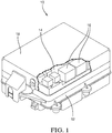
Fig. 1 is cut-away perspective view of an electrical center in accordance with one embodiment; -
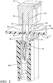
Fig. 2 is a cut-away view of a printed circuit board (PCB) assembly of the electrical center ofFig. 1 in accordance with one embodiment; -
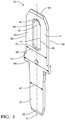
Fig. 3 is a perspective view of a double-ended male blade electrical terminal of the printed circuit board (PCB) assembly ofFig. 2 in accordance with one embodiment; -
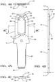
Fig. 4A is view of the double-ended male blade electrical terminal ofFig. 3 in accordance with one embodiment; -
Fig. 4B is end view of the double-ended male blade electrical terminal ofFig. 3 in accordance with one embodiment; -
Fig. 4C is cross sectional view of the double-ended male blade electrical terminal ofFig. 3 in accordance with one embodiment; and -
Fig. 4D is side view of the double-ended male blade electrical terminal ofFig. 3 in accordance with one embodiment; -
Fig. 5 is a flow chart of a method of manufacturing a double-ended male blade electrical terminal in accordance with another embodiment. - A double-ended male blade electrical terminal is presented herein. The terminal has two terminal blades with different effective thickness. The electrical terminal is suited for use in the printed circuit board of a vehicle's electrical center. A first blade of the terminal having a first thickness may be used to connect to a mating socket connector of the vehicle's wiring harness on one side of the PCB while a second blade having the different second thickness on the other side of the PCB may plug directly into the socket connector of an electrical device such as a fuse of a relay. This terminal eliminates the need for two separate blade terminals with different thickness and reduces the PCB real estate and conductive traces required to mount and connect them.
-
Fig. 1 illustrates a non-limiting example of anelectrical center 10 configured for use in a motor vehicle (not shown). The electrical center includes ahousing 12 containing a printed circuit board (PCB)assembly 14. ThePCB assembly 14 contains conductive traces (not shown) configured to connectelectronic devices 16, such as a relay or fuse, and electrical terminals (not shown) which may or may not be connected to the conductive traces. The PCB may be made from epoxy or polyimide resins. The resin may be reinforced with a woven glass cloth or other matrix such as chopped fibers. PCBs formed of such materials are typically called FR-4 or G-10 type circuit boards. The PCB may alternately be constructed of ceramic or rigid polymers. This listing of acceptable PCB materials is not exhaustive and other materials may also be used successfully. The materials and manufacturing techniques used to form printed circuit boards are well known to those skilled in the art. The electrical center also includes acover 18 that can be removed top allow access to the electronic devices as may be required for installation and service of the electronic devices. The electronic devices are located on oneside 20 of the PCB while the electrical terminals configured to interconnect theelectrical center 10 to the vehicle's wiring harness connectors are located on theopposite side 22 of the PCB. -
Fig. 2 illustrates non-limiting example of thePCB assembly 14 in a cut-away view wherein anelectronic device 16, such as a fuse, having a firstfemale socket terminal 24 is directly connected to anotherfemale socket terminal 26 in awiring harness connector 28 by a double-endedmale blade terminal 30 mounted though anaperture 32 or "via" in the PCB. Afirst blade 40 protrudes from afirst surface 20 of the PCB and thesecond blade 42 protrudes from asecond surface 22 of the PCB opposite thefirst surface 20. Asecond socket terminal 34 of theelectronic device 16 is connected to a single-endedmale blade terminal 36 that is mounted on thefirst surface 20 of the PCB. Both the double-endedmale blade terminal 30 and the single-endedmale blade terminal 36 are formed of a conductive material, such as copper alloys, brass, or beryllium copper. The double-endedterminal 30 and single-endedterminal 36 may be plated, for example with a tin-based alloy, to provide corrosion resistance. In example illustrated inFig. 2 , the double-endedterminal 30 is not connected to a PCB trace while the single-endedterminal 36 is connected to aPCB trace 38. Alternative embodiments of the PCB assembly may be envisioned wherein the double-ended male blade terminal is connected to a conductive trace on the PCB. - As shown in
Fig. 4D , thefirst blade 40 of the double-endedterminal 30 connected to the firstfemale socket terminal 24 of theelectronic device 16 has a substantially uniform first thickness T1, according to the illustrated example about 0.8 mm (0.8 +0.052/- 0.000 mm). As used herein, a uniform thickness is ± 0.026 mm Thesecond blade 42 of the double-endedterminal 30 configured to be connected to thefemale socket terminal 26 in awiring harness connector 28 hasregion 44 in the central, or mesial, portion of thesecond blade 42 wherein thesecond blade 42 is embossed or raised from the surrounding material of thesecond blade 42. This embossedregion 44 increases the effective thickness of thesecond blade 42 to a uniform second thickness T2, according to the illustrated example about 1.2 mm (1.2 ± 0.026 mm), which is greater than the first thickness T1. As used herein, embossed means that thesecond blade 42 is deformed by punch, die, or other metal deforming process so that afirst side 46 of thesecond blade 42 has a protrudedregion 48 while asecond side 50 opposite thefirst side 46 defines a correspondingindented region 52. - As best illustrated in
Figs 4B and 4C , the embossedregion 44 contains aplanar portion 54 that is parallel to thefirst side 46 and thesecond side 50 of thesecond blade 42. A second side of thefirst blade 40 is coplanar with the second side of thesecond blade 42. The second thickness T2 is the distance from the first side of thesecond blade 42 to theplanar portion 54 of the embossedregion 44. The embossedregion 44 is substantially non-compliant and is continuously attached to thesecond blade 42. As used herein, substantially non-compliant means that the embossedregion 44 will not deform under forces exerted on it by the mating socket connector in normal operation. The embossedregion 44 is not characterized as an arcuate fixed beam or a cantilevered beam. The embossedregion 44 is not configured to exert a spring force against the correspondingmating socket terminal 26; rather the correspondingmating socket terminal 26 is configured to exert a spring force against thesecond blade 42, including the embossedregion 44. - As best shown in
Figs. 4A and 4D , a firstdistal end 56 at the tip of thefirst blade 40 and a seconddistal end 58 at the tip of thesecond blade 42 are beveled, that is angled, so as to reduce the thickness T1 and the width W1, W2 of theblades blades mating socket terminals - As shown in
Fig. 4A , a leadingend 60 of the embossedregion 44 that is proximate, or nearest to, the seconddistal end 58 of thesecond blade 42 defines a roundedisosceles triangle shape 62. In the illustrated example, twosides 64 of theleading end 60 of the embossedregion 44 define a 30 degree angle relative to a longitudinal axis A of the double-endedterminal 30. Thetriangular shape 62 of theleading end 60 facilitates insertion of thesecond blade 42 into the correspondingmating socket terminal 26. Thesides 66 of the embossedregion 44 are substantially parallel to thesides 68 of thesecond blade 42. A trailingend 70 of the embossedregion 44 is characterized as having roundedcorners 72. Therounded corners 72 of the trailingend 70 facilitate removal of thesecond blade 42 from the correspondingmating socket terminal 26 during disconnection. - Returning now to
Fig. 3 , the double-endedterminal 30 defines ashoulder 74 intermediate thefirst blade 40 and thesecond blade 42. Thisshoulder 74 has ashoulder 74 width Ws that is greater than afirst blade 40 width W1 and asecond blade 42 width W2. According to the illustrated example, thesecond blade 42 width W2 is greater than thefirst blade 40 width W1. Alternatively, the shoulder may be defined by the wider of the first or second blades. Alternative embodiments of the electrical terminal may have a first blade that is wider than a second blade having an embossed region to increase thickness of the second blade or may have a first blade with the same width as a second blade. Theshoulder 74 may be mechanically and/or electrically attached to a copper pad on the PCB surrounding theaperture 32 by a soldering process. -
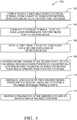
Fig. 5 illustrates a non-limiting example of amethod 100 of manufacturing a double-ended male bladeelectrical terminal 30 having afirst blade 40 with a uniform first thickness T1 and asecond blade 42 characterized by a uniform second thickness T2, wherein the effective thickness of thesecond blade 42 is greater than the thickness of thefirst blade 40. Themethod 100 includes the following steps: -
STEP 102, FORM A DOUBLE-ENDED MALE BLADE ELECTRICAL TERMINAL FROM A SHEET OF CONDUCTIVE MATERIAL HAVING A UNIFORM FIRST THICKNESS, includes forming the double-ended terminal 30 from a sheet of conductive material having the uniform first thickness T1. The double-endedterminal 30 may be formed from a sheet of a conductive material, such as copper alloys, brass, or beryllium copper. The double-endedterminal 30 may be formed by cutting, stamping, fine blanking, or any other method of forming a terminal blank from a sheet of conductive material known to those skilled in the art. According to one particular embodiment the first thickness T1 of the sheet is about 0.8 mm (0.8 +0.052/- 0.0 mm). The second blade width W2 may be greater than the first blade width W1 and one side of thefirst blade 40 and one side of thesecond blade 42 may be coplanar. -
STEP 104, FORM THE ELECTRICAL TERMINAL TO DEFINE A SHOULDER INTERMEDIATE THE FIRST BLADE AND THE SECOND BLADE, is an optional step that includes forming the double-endedelectrical terminal 30 to define ashoulder 74 intermediate thefirst blade 40 and thesecond blade 42, wherein theshoulder 74 has a width Ws that is greater than a first blade width W1 and a second blade width W2. -
STEP 106, BEVEL A FIRST DISTAL END OF THE FIRST BLADE AND A SECOND DISTAL END OF THE SECOND BLADE, is an optional step that includes beveling a firstdistal end 56 on the tip of thefirst blade 40 and a seconddistal end 58 on the tip of thesecond blade 42. -
STEP 108, EMBOSS A MESIAL REGION OF THE SECOND BLADE SO THAT THE MESIAL REGION IS CHARACTERIZED BY A UNIFORM SECOND THICKNESS, WHEREIN THE SECOND THICKNESS IS GREATER THAN THE FIRST THICKNESS includes embossing a centralmesial region 44 of thesecond blade 42 so that the embossedmesial region 44 is characterized by the uniform second thickness. The embossedregion 44 may be formed using conventional embossing methods such as a punch and die. According to one particular embodiment, the embossedregion 44 provides a second thickness is about 1.2 mm (1.2 ± 0.026 mm) from a second side of thesecond blade 42 to aplanar portion 54 of the embossedregion 44. -
STEP 110, EMBOSS A LEADING END OF THE EMBOSSED REGION PROXIMATE THE SECOND DISTAL END TO DEFINE A ROUNDED ISOSCELES TRIANGLE SHAPE, includes embossing aleading end 60 of the embossedregion 44 proximate the seconddistal end 58 to define a roundedisosceles triangle shape 62. According to one particular embodiment, twosides 64 of theleading end 60 of the embossedregion 44 define a 30 degree angle relative to a longitudinal axis A of the double-endedterminal 30. -
STEP 112, EMBOSS A TRAILING END OF THE EMBOSSED REGION TO DEFINE A PAIR OF ROUNDED CORNERS, includes embossing a trailingend 70 of the embossedregion 44 to define a pair ofrounded corners 72, wherein thesides 66 of the embossedregion 44 are substantially parallel to thesides 68 of thesecond blade 42. - While the examples of the double-ended male blade terminal are illustrated within a PCB assembly that is part of a vehicle electrical center, other embodiments of the double-ended male blade terminal made be envisioned wherein the PCB is used in applications other than a vehicle electrical center or wherein the double-ended male blade terminal is used to directly connect two corresponding socket connectors without a PCB.
- Accordingly, a
PCB assembly 14, a double-ended male bladeelectrical terminal 30, and amethod 100 of manufacturing such a terminal are provided. The double-endedterminal 30 of thePCB assembly 14 provides the benefit of directly connecting afemale socket terminal 26 in awiring harness connector 28 to afemale socket terminal 24 in anelectronic device 16 of thePCB assembly 14, such as a fuse or relay, wherein thefemale socket terminal 26 of thewiring harness connector 28 requires a different male blade terminal thickness than the socket terminal of the electrical device. The double-endedterminal 30 does not require as much "real estate", i.e. space on thesurfaces PCB assembly 14 as two separate male blade terminals mounted on each side of the PCB and does not require a conductive trace on the PCB in order to interconnect thefemale socket terminal 26 of thewiring harness connector 28 to theelectronic device 16. Themethod 100 of manufacturing the double-endedterminal 30 provides the benefit of forming the double-ended terminal 30 from a sheet of conductive material having a single uniform thickness using conventional metal forming techniques such as stamping and embossing. - The use of the terms first, second, etc. does not denote any order of importance, but rather the terms first, second, etc. are used to distinguish one element from another. Furthermore, the use of the terms a, an, etc. do not denote a limitation of quantity, but rather denote the presence of at least one of the referenced items.
Claims (11)
- Double-ended male blade electrical terminal (30), comprising:a first blade (40) wherein the first blade is configured to be connected to a corresponding socket terminal within an electrical device, having a uniform first thickness (T1); anda second blade (42) wherein the second blade is configured to be connected to a corresponding socket terminal within an electrical connector, having an embossed mesial region (44) that characterizes a uniform second thickness (T2), wherein the second thickness (T2) is greater than the first thickness (T1), characterized in that a first distal end (56) of the first blade (40) and a second distal end (58) of the second blade (42) are beveled and wherein a leading end (60) of the embossed region (44) proximate the second distal end (58) defines a rounded isosceles triangle shape (62), sides (66) of the embossed region (44) are parallel to sides (68) of the second blade (42) and a trailing end (70) of the embossed region (44) is having rounded corners (72).
- Electrical terminal (30) in accordance with claim 1, wherein the first thickness (T1) is about 0.8 millimeters and the second thickness (T2) is about 1.2 millimeters.
- Electrical terminal (30) in accordance with any of claims 1-2, wherein one side of the first blade (40) and one side of the second blade (42) are coplanar.
- Electrical terminal (30) in accordance with any of claims 1-3, wherein the electrical terminal (30) defines a shoulder (74) intermediate the first blade (40) and the second blade (42), said shoulder (74) having a shoulder width (Ws) that is greater than a first blade width (W1) and a second blade width (W2).
- Electrical terminal (30) in accordance with claim 1, wherein two sides (64) of the leading end (60) of the embossed region (44) define a 30 degree angle relative to a longitudinal axis of the electrical terminal (30).
- Electrical terminal (30) in accordance with any of claims 4-5, wherein the second blade width (W2) is greater than the first blade width (W1).
- Printed circuit board (PCB) assembly (14), comprising:a dielectric substrate (20);a conductive trace (38) disposed upon a surface of the substrate (20); anda double-ended male blade electrical terminal (30) according to any of claims 1-6, said electrical terminal (30) disposed within an aperture (32) defined by the substrate (20, wherein the second blade (42) is configured to be connected to a corresponding socket terminal within an electrical connector and wherein the first blade (40) is configured to be connected to a corresponding socket terminal within an electrical device.
- PCB assembly (14) in accordance with claim 7, wherein the first blade (40) protrudes from a first surface (20) of the substrate (20) and the second blade (42) protrudes from a second surface (22) of the substrate (20) opposite the first surface (20).
- PCB assembly (14) in accordance with claim 8, wherein the electrical device includes a fusible link and/or an electromechanical relay.
- Method (100) of manufacturing a double-ended male blade electrical terminal (30) according to any of claims 1-6, said method (100) comprising the steps of:forming (102) the double-ended male blade electrical terminal (30) from a sheet of conductive material having the uniform first thickness (T1); andembossing (108) a mesial region (44) of the second blade (42) so that the mesial region (44) is characterized by the uniform second thickness (T2, further comprising the steps of:beveling (106) a first distal end (56) of the first blade (40) and a second distal end (58) of the second blade (42);characterized by the steps: embossing (110) a leading end (60) of the embossed region (44) proximate the second distal end (58) to define a rounded isosceles triangle shape (62); andembossing (112) a trailing end (70) of the embossed region (44) to define a pair of rounded corners (72), wherein sides (66) of the embossed region (44) are parallel to sides (68) of the second blade (42)).
- Method (100) in accordance with claim 10, further comprising the step of forming (104) the electrical terminal (30) to define a shoulder (74) intermediate the first blade (40) and the second blade (42), said shoulder (74) having a shoulder width (Ws) that is greater than a first blade width (W1) and a second blade width (W2).
Applications Claiming Priority (1)
| Application Number | Priority Date | Filing Date | Title |
|---|---|---|---|
| US14/321,922 US9331413B2 (en) | 2014-07-02 | 2014-07-02 | Dual thickness double-ended male blade terminal |
Publications (2)
| Publication Number | Publication Date |
|---|---|
| EP2963739A1 EP2963739A1 (en) | 2016-01-06 |
| EP2963739B1 true EP2963739B1 (en) | 2018-12-19 |
Family
ID=53539484
Family Applications (1)
| Application Number | Title | Priority Date | Filing Date |
|---|---|---|---|
| EP15173604.8A Active EP2963739B1 (en) | 2014-07-02 | 2015-06-24 | Dual thickness double-ended male blade terminal and method of manufacturing it |
Country Status (6)
| Country | Link |
|---|---|
| US (1) | US9331413B2 (en) |
| EP (1) | EP2963739B1 (en) |
| JP (1) | JP6124953B2 (en) |
| KR (1) | KR101683386B1 (en) |
| CN (1) | CN105322330B (en) |
| BR (1) | BR102015013010A2 (en) |
Families Citing this family (5)
| Publication number | Priority date | Publication date | Assignee | Title |
|---|---|---|---|---|
| JP6183667B2 (en) * | 2015-10-01 | 2017-08-23 | 住友電装株式会社 | connector |
| US10349539B2 (en) * | 2017-10-03 | 2019-07-09 | Aptiv Technologies Limited | Vehicle electrical center and method of manufacturing same |
| EP3637564B1 (en) | 2018-10-08 | 2021-06-09 | Aptiv Technologies Limited | Process of manufacturing an electrical wiring assembly |
| CN117293575A (en) * | 2020-03-26 | 2023-12-26 | 上海莫仕连接器有限公司 | Electric connection device and terminal |
| US20210408710A1 (en) * | 2020-06-29 | 2021-12-30 | Microsoft Technology Licensing, Llc | Systems and methods for improving safety on electronic device connections |
Family Cites Families (22)
| Publication number | Priority date | Publication date | Assignee | Title |
|---|---|---|---|---|
| US2130424A (en) * | 1936-06-29 | 1938-09-20 | Albert T Otto & Sons Inc | Attachment plug |
| US2752580A (en) | 1953-04-27 | 1956-06-26 | Charles A Shewmaker | Printed circuit board and terminal connections |
| US2811702A (en) | 1956-06-21 | 1957-10-29 | Malco Tool & Mfg Co | Terminal pin for printed circuit board |
| US3977075A (en) * | 1971-10-28 | 1976-08-31 | Amp Incorporated | Method of fabricating multi-layer printed circuit board |
| JPS5968187A (en) * | 1982-10-13 | 1984-04-18 | 富士通株式会社 | Terminal structure |
| US4923414A (en) | 1989-07-03 | 1990-05-08 | E. I. Du Pont De Nemours And Company | Compliant section for circuit board contact elements |
| US5023752A (en) * | 1989-10-31 | 1991-06-11 | General Motors Corporation | Electrical power distribution center |
| US5046960A (en) * | 1990-12-20 | 1991-09-10 | Amp Incorporated | High density connector system |
| US5207603A (en) * | 1992-06-02 | 1993-05-04 | Molex Incorporated | Dual thickness blade type electrical terminal |
| EP0713263B1 (en) * | 1994-11-17 | 2000-09-06 | Molex Incorporated | Self-locking mating terminal structure |
| US5582519A (en) * | 1994-12-15 | 1996-12-10 | The Whitaker Corporation | Make-first-break-last ground connections |
| US5831814A (en) | 1997-03-14 | 1998-11-03 | General Motors Corporation | Electrical center bus plate assembly |
| US6008982A (en) * | 1998-05-20 | 1999-12-28 | General Motors Corporation | Low profile electrical distribution center and method of making a bus subassembly therefor |
| US6062916A (en) * | 1998-07-14 | 2000-05-16 | General Motors Corporation | Printed circuit board with pass through bussed terminal system for a bussed electrical distribution center |
| JP2002058134A (en) * | 2000-08-09 | 2002-02-22 | Auto Network Gijutsu Kenkyusho:Kk | Installation structure for electric control unit |
| US7955133B2 (en) * | 2008-04-23 | 2011-06-07 | Littelfuse, Inc. | Flexible power distribution module |
| JP5077190B2 (en) * | 2008-10-28 | 2012-11-21 | 住友電装株式会社 | Printed board |
| JP5224067B2 (en) * | 2009-11-11 | 2013-07-03 | 住友電装株式会社 | Board terminal and board connector having the same |
| JP5570395B2 (en) | 2010-10-08 | 2014-08-13 | モレックス インコーポレイテド | Sheet connector |
| US20120268864A1 (en) | 2011-04-21 | 2012-10-25 | Delphi Technologies, Inc. | Apparatus having plurality of openings to access removable electronic devices some of which have electrical connections using no circuit board trace |
| US8961197B2 (en) * | 2012-06-08 | 2015-02-24 | Lear Corporation | Fuse housing assembly |
| CN202662858U (en) * | 2012-06-25 | 2013-01-09 | 德尔福派克电气系统有限公司 | Conducting part contact mechanism of high-current product |
-
2014
- 2014-07-02 US US14/321,922 patent/US9331413B2/en active Active
-
2015
- 2015-06-03 BR BR102015013010A patent/BR102015013010A2/en not_active Application Discontinuation
- 2015-06-12 CN CN201510323420.8A patent/CN105322330B/en active Active
- 2015-06-24 EP EP15173604.8A patent/EP2963739B1/en active Active
- 2015-06-29 KR KR1020150091744A patent/KR101683386B1/en active IP Right Grant
- 2015-07-01 JP JP2015132463A patent/JP6124953B2/en active Active
Non-Patent Citations (1)
| Title |
|---|
| None * |
Also Published As
| Publication number | Publication date |
|---|---|
| US20160006155A1 (en) | 2016-01-07 |
| CN105322330A (en) | 2016-02-10 |
| US9331413B2 (en) | 2016-05-03 |
| CN105322330B (en) | 2018-06-12 |
| JP2016028381A (en) | 2016-02-25 |
| KR20160004196A (en) | 2016-01-12 |
| EP2963739A1 (en) | 2016-01-06 |
| KR101683386B1 (en) | 2016-12-06 |
| BR102015013010A2 (en) | 2016-07-19 |
| JP6124953B2 (en) | 2017-05-10 |
Similar Documents
| Publication | Publication Date | Title |
|---|---|---|
| US6062916A (en) | Printed circuit board with pass through bussed terminal system for a bussed electrical distribution center | |
| EP2963739B1 (en) | Dual thickness double-ended male blade terminal and method of manufacturing it | |
| CN101364679B (en) | Electrical connection assembly | |
| EP1506597B1 (en) | Electrical power connector | |
| US7556543B2 (en) | One-piece PC board magnet wire terminal | |
| JP5140125B2 (en) | Connector terminal manufacturing method and connector terminal | |
| EP2284952A1 (en) | High frequency module and wireless device | |
| JP2005353567A (en) | Press-fit terminal and circuit board module using it | |
| US11050200B2 (en) | Electrical connector with hermaphroditic terminal and housing | |
| KR200293510Y1 (en) | Electrical Connector Assembly having Terminal Pins Mounted in Flexible Substrate | |
| US8371871B1 (en) | Terminal with compliant barb | |
| US20160181710A1 (en) | Printed Circuit Board Assembly Having Improved Terminals | |
| KR100304514B1 (en) | Method of fabricating electronic device employing a flat flexible circuit and including the device itself | |
| US6203386B1 (en) | Terminal blades mounted on flexible substrates | |
| JP5622051B2 (en) | Board terminal and board connector using the same | |
| US20170346203A1 (en) | Board terminal | |
| US11791575B2 (en) | Circuit board with U-shaped electrical terminal | |
| US20240120671A1 (en) | Connector and electronic device | |
| US20140291002A1 (en) | Printed circuit board module | |
| JP2023167498A (en) | Wiring connection method and plug connector | |
| WO2013004576A1 (en) | Electrical contact element | |
| CN115693320A (en) | Connection structure between members | |
| JP2008277040A (en) | Connector | |
| JP2015201333A (en) | connector terminal | |
| JP2018055938A (en) | Electronic device and pressure contact terminal |
Legal Events
| Date | Code | Title | Description |
|---|---|---|---|
| PUAI | Public reference made under article 153(3) epc to a published international application that has entered the european phase |
Free format text: ORIGINAL CODE: 0009012 |
|
| AK | Designated contracting states |
Kind code of ref document: A1 Designated state(s): AL AT BE BG CH CY CZ DE DK EE ES FI FR GB GR HR HU IE IS IT LI LT LU LV MC MK MT NL NO PL PT RO RS SE SI SK SM TR |
|
| AX | Request for extension of the european patent |
Extension state: BA ME |
|
| 17P | Request for examination filed |
Effective date: 20160706 |
|
| RBV | Designated contracting states (corrected) |
Designated state(s): AL AT BE BG CH CY CZ DE DK EE ES FI FR GB GR HR HU IE IS IT LI LT LU LV MC MK MT NL NO PL PT RO RS SE SI SK SM TR |
|
| STAA | Information on the status of an ep patent application or granted ep patent |
Free format text: STATUS: EXAMINATION IS IN PROGRESS |
|
| 17Q | First examination report despatched |
Effective date: 20180125 |
|
| GRAP | Despatch of communication of intention to grant a patent |
Free format text: ORIGINAL CODE: EPIDOSNIGR1 |
|
| STAA | Information on the status of an ep patent application or granted ep patent |
Free format text: STATUS: GRANT OF PATENT IS INTENDED |
|
| RIC1 | Information provided on ipc code assigned before grant |
Ipc: H01R 13/05 20060101ALI20180705BHEP Ipc: H01R 13/04 20060101ALI20180705BHEP Ipc: H01R 12/58 20110101AFI20180705BHEP Ipc: H01R 43/16 20060101ALI20180705BHEP |
|
| INTG | Intention to grant announced |
Effective date: 20180731 |
|
| GRAS | Grant fee paid |
Free format text: ORIGINAL CODE: EPIDOSNIGR3 |
|
| GRAA | (expected) grant |
Free format text: ORIGINAL CODE: 0009210 |
|
| STAA | Information on the status of an ep patent application or granted ep patent |
Free format text: STATUS: THE PATENT HAS BEEN GRANTED |
|
| AK | Designated contracting states |
Kind code of ref document: B1 Designated state(s): AL AT BE BG CH CY CZ DE DK EE ES FI FR GB GR HR HU IE IS IT LI LT LU LV MC MK MT NL NO PL PT RO RS SE SI SK SM TR |
|
| RAP1 | Party data changed (applicant data changed or rights of an application transferred) |
Owner name: APTIV TECHNOLOGIES LIMITED |
|
| REG | Reference to a national code |
Ref country code: GB Ref legal event code: FG4D |
|
| REG | Reference to a national code |
Ref country code: CH Ref legal event code: EP |
|
| REG | Reference to a national code |
Ref country code: IE Ref legal event code: FG4D |
|
| REG | Reference to a national code |
Ref country code: DE Ref legal event code: R096 Ref document number: 602015021765 Country of ref document: DE |
|
| REG | Reference to a national code |
Ref country code: AT Ref legal event code: REF Ref document number: 1079689 Country of ref document: AT Kind code of ref document: T Effective date: 20190115 |
|
| REG | Reference to a national code |
Ref country code: NL Ref legal event code: MP Effective date: 20181219 |
|
| PG25 | Lapsed in a contracting state [announced via postgrant information from national office to epo] |
Ref country code: FI Free format text: LAPSE BECAUSE OF FAILURE TO SUBMIT A TRANSLATION OF THE DESCRIPTION OR TO PAY THE FEE WITHIN THE PRESCRIBED TIME-LIMIT Effective date: 20181219 Ref country code: HR Free format text: LAPSE BECAUSE OF FAILURE TO SUBMIT A TRANSLATION OF THE DESCRIPTION OR TO PAY THE FEE WITHIN THE PRESCRIBED TIME-LIMIT Effective date: 20181219 Ref country code: NO Free format text: LAPSE BECAUSE OF FAILURE TO SUBMIT A TRANSLATION OF THE DESCRIPTION OR TO PAY THE FEE WITHIN THE PRESCRIBED TIME-LIMIT Effective date: 20190319 Ref country code: LV Free format text: LAPSE BECAUSE OF FAILURE TO SUBMIT A TRANSLATION OF THE DESCRIPTION OR TO PAY THE FEE WITHIN THE PRESCRIBED TIME-LIMIT Effective date: 20181219 Ref country code: BG Free format text: LAPSE BECAUSE OF FAILURE TO SUBMIT A TRANSLATION OF THE DESCRIPTION OR TO PAY THE FEE WITHIN THE PRESCRIBED TIME-LIMIT Effective date: 20190319 Ref country code: LT Free format text: LAPSE BECAUSE OF FAILURE TO SUBMIT A TRANSLATION OF THE DESCRIPTION OR TO PAY THE FEE WITHIN THE PRESCRIBED TIME-LIMIT Effective date: 20181219 |
|
| REG | Reference to a national code |
Ref country code: LT Ref legal event code: MG4D |
|
| REG | Reference to a national code |
Ref country code: AT Ref legal event code: MK05 Ref document number: 1079689 Country of ref document: AT Kind code of ref document: T Effective date: 20181219 |
|
| PG25 | Lapsed in a contracting state [announced via postgrant information from national office to epo] |
Ref country code: AL Free format text: LAPSE BECAUSE OF FAILURE TO SUBMIT A TRANSLATION OF THE DESCRIPTION OR TO PAY THE FEE WITHIN THE PRESCRIBED TIME-LIMIT Effective date: 20181219 Ref country code: GR Free format text: LAPSE BECAUSE OF FAILURE TO SUBMIT A TRANSLATION OF THE DESCRIPTION OR TO PAY THE FEE WITHIN THE PRESCRIBED TIME-LIMIT Effective date: 20190320 Ref country code: SE Free format text: LAPSE BECAUSE OF FAILURE TO SUBMIT A TRANSLATION OF THE DESCRIPTION OR TO PAY THE FEE WITHIN THE PRESCRIBED TIME-LIMIT Effective date: 20181219 Ref country code: RS Free format text: LAPSE BECAUSE OF FAILURE TO SUBMIT A TRANSLATION OF THE DESCRIPTION OR TO PAY THE FEE WITHIN THE PRESCRIBED TIME-LIMIT Effective date: 20181219 |
|
| PG25 | Lapsed in a contracting state [announced via postgrant information from national office to epo] |
Ref country code: NL Free format text: LAPSE BECAUSE OF FAILURE TO SUBMIT A TRANSLATION OF THE DESCRIPTION OR TO PAY THE FEE WITHIN THE PRESCRIBED TIME-LIMIT Effective date: 20181219 |
|
| PG25 | Lapsed in a contracting state [announced via postgrant information from national office to epo] |
Ref country code: IT Free format text: LAPSE BECAUSE OF FAILURE TO SUBMIT A TRANSLATION OF THE DESCRIPTION OR TO PAY THE FEE WITHIN THE PRESCRIBED TIME-LIMIT Effective date: 20181219 Ref country code: CZ Free format text: LAPSE BECAUSE OF FAILURE TO SUBMIT A TRANSLATION OF THE DESCRIPTION OR TO PAY THE FEE WITHIN THE PRESCRIBED TIME-LIMIT Effective date: 20181219 Ref country code: PT Free format text: LAPSE BECAUSE OF FAILURE TO SUBMIT A TRANSLATION OF THE DESCRIPTION OR TO PAY THE FEE WITHIN THE PRESCRIBED TIME-LIMIT Effective date: 20190419 Ref country code: PL Free format text: LAPSE BECAUSE OF FAILURE TO SUBMIT A TRANSLATION OF THE DESCRIPTION OR TO PAY THE FEE WITHIN THE PRESCRIBED TIME-LIMIT Effective date: 20181219 Ref country code: ES Free format text: LAPSE BECAUSE OF FAILURE TO SUBMIT A TRANSLATION OF THE DESCRIPTION OR TO PAY THE FEE WITHIN THE PRESCRIBED TIME-LIMIT Effective date: 20181219 |
|
| PG25 | Lapsed in a contracting state [announced via postgrant information from national office to epo] |
Ref country code: EE Free format text: LAPSE BECAUSE OF FAILURE TO SUBMIT A TRANSLATION OF THE DESCRIPTION OR TO PAY THE FEE WITHIN THE PRESCRIBED TIME-LIMIT Effective date: 20181219 Ref country code: SM Free format text: LAPSE BECAUSE OF FAILURE TO SUBMIT A TRANSLATION OF THE DESCRIPTION OR TO PAY THE FEE WITHIN THE PRESCRIBED TIME-LIMIT Effective date: 20181219 Ref country code: RO Free format text: LAPSE BECAUSE OF FAILURE TO SUBMIT A TRANSLATION OF THE DESCRIPTION OR TO PAY THE FEE WITHIN THE PRESCRIBED TIME-LIMIT Effective date: 20181219 Ref country code: SK Free format text: LAPSE BECAUSE OF FAILURE TO SUBMIT A TRANSLATION OF THE DESCRIPTION OR TO PAY THE FEE WITHIN THE PRESCRIBED TIME-LIMIT Effective date: 20181219 Ref country code: IS Free format text: LAPSE BECAUSE OF FAILURE TO SUBMIT A TRANSLATION OF THE DESCRIPTION OR TO PAY THE FEE WITHIN THE PRESCRIBED TIME-LIMIT Effective date: 20190419 |
|
| REG | Reference to a national code |
Ref country code: DE Ref legal event code: R097 Ref document number: 602015021765 Country of ref document: DE |
|
| PLBE | No opposition filed within time limit |
Free format text: ORIGINAL CODE: 0009261 |
|
| STAA | Information on the status of an ep patent application or granted ep patent |
Free format text: STATUS: NO OPPOSITION FILED WITHIN TIME LIMIT |
|
| PG25 | Lapsed in a contracting state [announced via postgrant information from national office to epo] |
Ref country code: DK Free format text: LAPSE BECAUSE OF FAILURE TO SUBMIT A TRANSLATION OF THE DESCRIPTION OR TO PAY THE FEE WITHIN THE PRESCRIBED TIME-LIMIT Effective date: 20181219 Ref country code: AT Free format text: LAPSE BECAUSE OF FAILURE TO SUBMIT A TRANSLATION OF THE DESCRIPTION OR TO PAY THE FEE WITHIN THE PRESCRIBED TIME-LIMIT Effective date: 20181219 |
|
| 26N | No opposition filed |
Effective date: 20190920 |
|
| PG25 | Lapsed in a contracting state [announced via postgrant information from national office to epo] |
Ref country code: MC Free format text: LAPSE BECAUSE OF FAILURE TO SUBMIT A TRANSLATION OF THE DESCRIPTION OR TO PAY THE FEE WITHIN THE PRESCRIBED TIME-LIMIT Effective date: 20181219 |
|
| REG | Reference to a national code |
Ref country code: CH Ref legal event code: PL |
|
| PG25 | Lapsed in a contracting state [announced via postgrant information from national office to epo] |
Ref country code: SI Free format text: LAPSE BECAUSE OF FAILURE TO SUBMIT A TRANSLATION OF THE DESCRIPTION OR TO PAY THE FEE WITHIN THE PRESCRIBED TIME-LIMIT Effective date: 20181219 |
|
| REG | Reference to a national code |
Ref country code: BE Ref legal event code: MM Effective date: 20190630 |
|
| PG25 | Lapsed in a contracting state [announced via postgrant information from national office to epo] |
Ref country code: TR Free format text: LAPSE BECAUSE OF FAILURE TO SUBMIT A TRANSLATION OF THE DESCRIPTION OR TO PAY THE FEE WITHIN THE PRESCRIBED TIME-LIMIT Effective date: 20181219 |
|
| PG25 | Lapsed in a contracting state [announced via postgrant information from national office to epo] |
Ref country code: IE Free format text: LAPSE BECAUSE OF NON-PAYMENT OF DUE FEES Effective date: 20190624 |
|
| PG25 | Lapsed in a contracting state [announced via postgrant information from national office to epo] |
Ref country code: CH Free format text: LAPSE BECAUSE OF NON-PAYMENT OF DUE FEES Effective date: 20190630 Ref country code: LI Free format text: LAPSE BECAUSE OF NON-PAYMENT OF DUE FEES Effective date: 20190630 Ref country code: BE Free format text: LAPSE BECAUSE OF NON-PAYMENT OF DUE FEES Effective date: 20190630 Ref country code: LU Free format text: LAPSE BECAUSE OF NON-PAYMENT OF DUE FEES Effective date: 20190624 |
|
| PG25 | Lapsed in a contracting state [announced via postgrant information from national office to epo] |
Ref country code: CY Free format text: LAPSE BECAUSE OF FAILURE TO SUBMIT A TRANSLATION OF THE DESCRIPTION OR TO PAY THE FEE WITHIN THE PRESCRIBED TIME-LIMIT Effective date: 20181219 |
|
| PG25 | Lapsed in a contracting state [announced via postgrant information from national office to epo] |
Ref country code: HU Free format text: LAPSE BECAUSE OF FAILURE TO SUBMIT A TRANSLATION OF THE DESCRIPTION OR TO PAY THE FEE WITHIN THE PRESCRIBED TIME-LIMIT; INVALID AB INITIO Effective date: 20150624 Ref country code: MT Free format text: LAPSE BECAUSE OF FAILURE TO SUBMIT A TRANSLATION OF THE DESCRIPTION OR TO PAY THE FEE WITHIN THE PRESCRIBED TIME-LIMIT Effective date: 20181219 |
|
| PG25 | Lapsed in a contracting state [announced via postgrant information from national office to epo] |
Ref country code: MK Free format text: LAPSE BECAUSE OF FAILURE TO SUBMIT A TRANSLATION OF THE DESCRIPTION OR TO PAY THE FEE WITHIN THE PRESCRIBED TIME-LIMIT Effective date: 20181219 |
|
| P01 | Opt-out of the competence of the unified patent court (upc) registered |
Effective date: 20230424 |
|
| PGFP | Annual fee paid to national office [announced via postgrant information from national office to epo] |
Ref country code: FR Payment date: 20230628 Year of fee payment: 9 Ref country code: DE Payment date: 20230621 Year of fee payment: 9 |
|
| PGFP | Annual fee paid to national office [announced via postgrant information from national office to epo] |
Ref country code: GB Payment date: 20230621 Year of fee payment: 9 |