EP2933836B1 - Power semiconductor module - Google Patents
Power semiconductor module Download PDFInfo
- Publication number
- EP2933836B1 EP2933836B1 EP14164812.1A EP14164812A EP2933836B1 EP 2933836 B1 EP2933836 B1 EP 2933836B1 EP 14164812 A EP14164812 A EP 14164812A EP 2933836 B1 EP2933836 B1 EP 2933836B1
- Authority
- EP
- European Patent Office
- Prior art keywords
- power semiconductor
- contact
- semiconductor module
- lug
- contact elements
- Prior art date
- Legal status (The legal status is an assumption and is not a legal conclusion. Google has not performed a legal analysis and makes no representation as to the accuracy of the status listed.)
- Active
Links
- 239000004065 semiconductor Substances 0.000 title claims description 53
- 239000000758 substrate Substances 0.000 claims description 23
- 229910000679 solder Inorganic materials 0.000 claims description 9
- 229910052751 metal Inorganic materials 0.000 claims description 8
- 239000002184 metal Substances 0.000 claims description 8
- 239000000919 ceramic Substances 0.000 claims description 3
- 238000007747 plating Methods 0.000 claims description 3
- 238000013459 approach Methods 0.000 description 16
- 238000005476 soldering Methods 0.000 description 10
- 238000000034 method Methods 0.000 description 8
- 238000005516 engineering process Methods 0.000 description 6
- 239000010949 copper Substances 0.000 description 5
- 238000001465 metallisation Methods 0.000 description 5
- 238000003466 welding Methods 0.000 description 5
- 229910052802 copper Inorganic materials 0.000 description 4
- RYGMFSIKBFXOCR-UHFFFAOYSA-N Copper Chemical compound [Cu] RYGMFSIKBFXOCR-UHFFFAOYSA-N 0.000 description 3
- PXHVJJICTQNCMI-UHFFFAOYSA-N Nickel Chemical compound [Ni] PXHVJJICTQNCMI-UHFFFAOYSA-N 0.000 description 2
- 229910052782 aluminium Inorganic materials 0.000 description 2
- 238000004519 manufacturing process Methods 0.000 description 2
- 230000000284 resting effect Effects 0.000 description 2
- 208000004067 Flatfoot Diseases 0.000 description 1
- XAGFODPZIPBFFR-UHFFFAOYSA-N aluminium Chemical compound [Al] XAGFODPZIPBFFR-UHFFFAOYSA-N 0.000 description 1
- 239000000969 carrier Substances 0.000 description 1
- 238000005266 casting Methods 0.000 description 1
- 239000011248 coating agent Substances 0.000 description 1
- 238000000576 coating method Methods 0.000 description 1
- 239000004020 conductor Substances 0.000 description 1
- 238000010276 construction Methods 0.000 description 1
- 230000001419 dependent effect Effects 0.000 description 1
- 238000010292 electrical insulation Methods 0.000 description 1
- 239000011521 glass Substances 0.000 description 1
- 230000017525 heat dissipation Effects 0.000 description 1
- 238000000465 moulding Methods 0.000 description 1
- 229910052759 nickel Inorganic materials 0.000 description 1
- 230000003647 oxidation Effects 0.000 description 1
- 238000007254 oxidation reaction Methods 0.000 description 1
- TWNQGVIAIRXVLR-UHFFFAOYSA-N oxo(oxoalumanyloxy)alumane Chemical compound O=[Al]O[Al]=O TWNQGVIAIRXVLR-UHFFFAOYSA-N 0.000 description 1
- 229920003002 synthetic resin Polymers 0.000 description 1
- 239000000057 synthetic resin Substances 0.000 description 1
Images


Classifications
-
- H—ELECTRICITY
- H01—ELECTRIC ELEMENTS
- H01L—SEMICONDUCTOR DEVICES NOT COVERED BY CLASS H10
- H01L25/00—Assemblies consisting of a plurality of individual semiconductor or other solid state devices ; Multistep manufacturing processes thereof
- H01L25/03—Assemblies consisting of a plurality of individual semiconductor or other solid state devices ; Multistep manufacturing processes thereof all the devices being of a type provided for in the same subgroup of groups H01L27/00 - H01L33/00, or in a single subclass of H10K, H10N, e.g. assemblies of rectifier diodes
- H01L25/04—Assemblies consisting of a plurality of individual semiconductor or other solid state devices ; Multistep manufacturing processes thereof all the devices being of a type provided for in the same subgroup of groups H01L27/00 - H01L33/00, or in a single subclass of H10K, H10N, e.g. assemblies of rectifier diodes the devices not having separate containers
- H01L25/07—Assemblies consisting of a plurality of individual semiconductor or other solid state devices ; Multistep manufacturing processes thereof all the devices being of a type provided for in the same subgroup of groups H01L27/00 - H01L33/00, or in a single subclass of H10K, H10N, e.g. assemblies of rectifier diodes the devices not having separate containers the devices being of a type provided for in group H01L29/00
- H01L25/072—Assemblies consisting of a plurality of individual semiconductor or other solid state devices ; Multistep manufacturing processes thereof all the devices being of a type provided for in the same subgroup of groups H01L27/00 - H01L33/00, or in a single subclass of H10K, H10N, e.g. assemblies of rectifier diodes the devices not having separate containers the devices being of a type provided for in group H01L29/00 the devices being arranged next to each other
-
- H—ELECTRICITY
- H01—ELECTRIC ELEMENTS
- H01L—SEMICONDUCTOR DEVICES NOT COVERED BY CLASS H10
- H01L23/00—Details of semiconductor or other solid state devices
- H01L23/34—Arrangements for cooling, heating, ventilating or temperature compensation ; Temperature sensing arrangements
- H01L23/36—Selection of materials, or shaping, to facilitate cooling or heating, e.g. heatsinks
- H01L23/373—Cooling facilitated by selection of materials for the device or materials for thermal expansion adaptation, e.g. carbon
- H01L23/3735—Laminates or multilayers, e.g. direct bond copper ceramic substrates
-
- H—ELECTRICITY
- H01—ELECTRIC ELEMENTS
- H01L—SEMICONDUCTOR DEVICES NOT COVERED BY CLASS H10
- H01L23/00—Details of semiconductor or other solid state devices
- H01L23/48—Arrangements for conducting electric current to or from the solid state body in operation, e.g. leads, terminal arrangements ; Selection of materials therefor
- H01L23/488—Arrangements for conducting electric current to or from the solid state body in operation, e.g. leads, terminal arrangements ; Selection of materials therefor consisting of soldered or bonded constructions
- H01L23/498—Leads, i.e. metallisations or lead-frames on insulating substrates, e.g. chip carriers
- H01L23/49811—Additional leads joined to the metallisation on the insulating substrate, e.g. pins, bumps, wires, flat leads
-
- H—ELECTRICITY
- H01—ELECTRIC ELEMENTS
- H01L—SEMICONDUCTOR DEVICES NOT COVERED BY CLASS H10
- H01L24/00—Arrangements for connecting or disconnecting semiconductor or solid-state bodies; Methods or apparatus related thereto
- H01L24/01—Means for bonding being attached to, or being formed on, the surface to be connected, e.g. chip-to-package, die-attach, "first-level" interconnects; Manufacturing methods related thereto
- H01L24/34—Strap connectors, e.g. copper straps for grounding power devices; Manufacturing methods related thereto
- H01L24/36—Structure, shape, material or disposition of the strap connectors prior to the connecting process
- H01L24/37—Structure, shape, material or disposition of the strap connectors prior to the connecting process of an individual strap connector
-
- H—ELECTRICITY
- H01—ELECTRIC ELEMENTS
- H01L—SEMICONDUCTOR DEVICES NOT COVERED BY CLASS H10
- H01L24/00—Arrangements for connecting or disconnecting semiconductor or solid-state bodies; Methods or apparatus related thereto
- H01L24/01—Means for bonding being attached to, or being formed on, the surface to be connected, e.g. chip-to-package, die-attach, "first-level" interconnects; Manufacturing methods related thereto
- H01L24/34—Strap connectors, e.g. copper straps for grounding power devices; Manufacturing methods related thereto
- H01L24/39—Structure, shape, material or disposition of the strap connectors after the connecting process
- H01L24/40—Structure, shape, material or disposition of the strap connectors after the connecting process of an individual strap connector
-
- H—ELECTRICITY
- H01—ELECTRIC ELEMENTS
- H01L—SEMICONDUCTOR DEVICES NOT COVERED BY CLASS H10
- H01L2224/00—Indexing scheme for arrangements for connecting or disconnecting semiconductor or solid-state bodies and methods related thereto as covered by H01L24/00
- H01L2224/01—Means for bonding being attached to, or being formed on, the surface to be connected, e.g. chip-to-package, die-attach, "first-level" interconnects; Manufacturing methods related thereto
- H01L2224/26—Layer connectors, e.g. plate connectors, solder or adhesive layers; Manufacturing methods related thereto
- H01L2224/28—Structure, shape, material or disposition of the layer connectors prior to the connecting process
- H01L2224/29—Structure, shape, material or disposition of the layer connectors prior to the connecting process of an individual layer connector
- H01L2224/29001—Core members of the layer connector
- H01L2224/29099—Material
- H01L2224/291—Material with a principal constituent of the material being a metal or a metalloid, e.g. boron [B], silicon [Si], germanium [Ge], arsenic [As], antimony [Sb], tellurium [Te] and polonium [Po], and alloys thereof
-
- H—ELECTRICITY
- H01—ELECTRIC ELEMENTS
- H01L—SEMICONDUCTOR DEVICES NOT COVERED BY CLASS H10
- H01L2224/00—Indexing scheme for arrangements for connecting or disconnecting semiconductor or solid-state bodies and methods related thereto as covered by H01L24/00
- H01L2224/01—Means for bonding being attached to, or being formed on, the surface to be connected, e.g. chip-to-package, die-attach, "first-level" interconnects; Manufacturing methods related thereto
- H01L2224/26—Layer connectors, e.g. plate connectors, solder or adhesive layers; Manufacturing methods related thereto
- H01L2224/31—Structure, shape, material or disposition of the layer connectors after the connecting process
- H01L2224/32—Structure, shape, material or disposition of the layer connectors after the connecting process of an individual layer connector
- H01L2224/321—Disposition
- H01L2224/32151—Disposition the layer connector connecting between a semiconductor or solid-state body and an item not being a semiconductor or solid-state body, e.g. chip-to-substrate, chip-to-passive
- H01L2224/32221—Disposition the layer connector connecting between a semiconductor or solid-state body and an item not being a semiconductor or solid-state body, e.g. chip-to-substrate, chip-to-passive the body and the item being stacked
- H01L2224/32225—Disposition the layer connector connecting between a semiconductor or solid-state body and an item not being a semiconductor or solid-state body, e.g. chip-to-substrate, chip-to-passive the body and the item being stacked the item being non-metallic, e.g. insulating substrate with or without metallisation
- H01L2224/32227—Disposition the layer connector connecting between a semiconductor or solid-state body and an item not being a semiconductor or solid-state body, e.g. chip-to-substrate, chip-to-passive the body and the item being stacked the item being non-metallic, e.g. insulating substrate with or without metallisation the layer connector connecting to a bond pad of the item
-
- H—ELECTRICITY
- H01—ELECTRIC ELEMENTS
- H01L—SEMICONDUCTOR DEVICES NOT COVERED BY CLASS H10
- H01L2224/00—Indexing scheme for arrangements for connecting or disconnecting semiconductor or solid-state bodies and methods related thereto as covered by H01L24/00
- H01L2224/01—Means for bonding being attached to, or being formed on, the surface to be connected, e.g. chip-to-package, die-attach, "first-level" interconnects; Manufacturing methods related thereto
- H01L2224/34—Strap connectors, e.g. copper straps for grounding power devices; Manufacturing methods related thereto
- H01L2224/36—Structure, shape, material or disposition of the strap connectors prior to the connecting process
- H01L2224/37—Structure, shape, material or disposition of the strap connectors prior to the connecting process of an individual strap connector
- H01L2224/37001—Core members of the connector
- H01L2224/3701—Shape
- H01L2224/37011—Shape comprising apertures or cavities
-
- H—ELECTRICITY
- H01—ELECTRIC ELEMENTS
- H01L—SEMICONDUCTOR DEVICES NOT COVERED BY CLASS H10
- H01L2224/00—Indexing scheme for arrangements for connecting or disconnecting semiconductor or solid-state bodies and methods related thereto as covered by H01L24/00
- H01L2224/01—Means for bonding being attached to, or being formed on, the surface to be connected, e.g. chip-to-package, die-attach, "first-level" interconnects; Manufacturing methods related thereto
- H01L2224/34—Strap connectors, e.g. copper straps for grounding power devices; Manufacturing methods related thereto
- H01L2224/36—Structure, shape, material or disposition of the strap connectors prior to the connecting process
- H01L2224/37—Structure, shape, material or disposition of the strap connectors prior to the connecting process of an individual strap connector
- H01L2224/37001—Core members of the connector
- H01L2224/3701—Shape
- H01L2224/37012—Cross-sectional shape
-
- H—ELECTRICITY
- H01—ELECTRIC ELEMENTS
- H01L—SEMICONDUCTOR DEVICES NOT COVERED BY CLASS H10
- H01L2224/00—Indexing scheme for arrangements for connecting or disconnecting semiconductor or solid-state bodies and methods related thereto as covered by H01L24/00
- H01L2224/01—Means for bonding being attached to, or being formed on, the surface to be connected, e.g. chip-to-package, die-attach, "first-level" interconnects; Manufacturing methods related thereto
- H01L2224/34—Strap connectors, e.g. copper straps for grounding power devices; Manufacturing methods related thereto
- H01L2224/36—Structure, shape, material or disposition of the strap connectors prior to the connecting process
- H01L2224/37—Structure, shape, material or disposition of the strap connectors prior to the connecting process of an individual strap connector
- H01L2224/37001—Core members of the connector
- H01L2224/37099—Material
- H01L2224/371—Material with a principal constituent of the material being a metal or a metalloid, e.g. boron [B], silicon [Si], germanium [Ge], arsenic [As], antimony [Sb], tellurium [Te] and polonium [Po], and alloys thereof
- H01L2224/37138—Material with a principal constituent of the material being a metal or a metalloid, e.g. boron [B], silicon [Si], germanium [Ge], arsenic [As], antimony [Sb], tellurium [Te] and polonium [Po], and alloys thereof the principal constituent melting at a temperature of greater than or equal to 950°C and less than 1550°C
- H01L2224/37147—Copper [Cu] as principal constituent
-
- H—ELECTRICITY
- H01—ELECTRIC ELEMENTS
- H01L—SEMICONDUCTOR DEVICES NOT COVERED BY CLASS H10
- H01L2224/00—Indexing scheme for arrangements for connecting or disconnecting semiconductor or solid-state bodies and methods related thereto as covered by H01L24/00
- H01L2224/01—Means for bonding being attached to, or being formed on, the surface to be connected, e.g. chip-to-package, die-attach, "first-level" interconnects; Manufacturing methods related thereto
- H01L2224/34—Strap connectors, e.g. copper straps for grounding power devices; Manufacturing methods related thereto
- H01L2224/36—Structure, shape, material or disposition of the strap connectors prior to the connecting process
- H01L2224/37—Structure, shape, material or disposition of the strap connectors prior to the connecting process of an individual strap connector
- H01L2224/3754—Coating
- H01L2224/37599—Material
- H01L2224/376—Material with a principal constituent of the material being a metal or a metalloid, e.g. boron [B], silicon [Si], germanium [Ge], arsenic [As], antimony [Sb], tellurium [Te] and polonium [Po], and alloys thereof
- H01L2224/37638—Material with a principal constituent of the material being a metal or a metalloid, e.g. boron [B], silicon [Si], germanium [Ge], arsenic [As], antimony [Sb], tellurium [Te] and polonium [Po], and alloys thereof the principal constituent melting at a temperature of greater than or equal to 950°C and less than 1550°C
- H01L2224/37655—Nickel [Ni] as principal constituent
-
- H—ELECTRICITY
- H01—ELECTRIC ELEMENTS
- H01L—SEMICONDUCTOR DEVICES NOT COVERED BY CLASS H10
- H01L2224/00—Indexing scheme for arrangements for connecting or disconnecting semiconductor or solid-state bodies and methods related thereto as covered by H01L24/00
- H01L2224/01—Means for bonding being attached to, or being formed on, the surface to be connected, e.g. chip-to-package, die-attach, "first-level" interconnects; Manufacturing methods related thereto
- H01L2224/34—Strap connectors, e.g. copper straps for grounding power devices; Manufacturing methods related thereto
- H01L2224/39—Structure, shape, material or disposition of the strap connectors after the connecting process
- H01L2224/40—Structure, shape, material or disposition of the strap connectors after the connecting process of an individual strap connector
- H01L2224/401—Disposition
- H01L2224/40135—Connecting between different semiconductor or solid-state bodies, i.e. chip-to-chip
- H01L2224/40137—Connecting between different semiconductor or solid-state bodies, i.e. chip-to-chip the bodies being arranged next to each other, e.g. on a common substrate
-
- H—ELECTRICITY
- H01—ELECTRIC ELEMENTS
- H01L—SEMICONDUCTOR DEVICES NOT COVERED BY CLASS H10
- H01L2224/00—Indexing scheme for arrangements for connecting or disconnecting semiconductor or solid-state bodies and methods related thereto as covered by H01L24/00
- H01L2224/01—Means for bonding being attached to, or being formed on, the surface to be connected, e.g. chip-to-package, die-attach, "first-level" interconnects; Manufacturing methods related thereto
- H01L2224/34—Strap connectors, e.g. copper straps for grounding power devices; Manufacturing methods related thereto
- H01L2224/39—Structure, shape, material or disposition of the strap connectors after the connecting process
- H01L2224/40—Structure, shape, material or disposition of the strap connectors after the connecting process of an individual strap connector
- H01L2224/401—Disposition
- H01L2224/40151—Connecting between a semiconductor or solid-state body and an item not being a semiconductor or solid-state body, e.g. chip-to-substrate, chip-to-passive
- H01L2224/40221—Connecting between a semiconductor or solid-state body and an item not being a semiconductor or solid-state body, e.g. chip-to-substrate, chip-to-passive the body and the item being stacked
- H01L2224/40225—Connecting between a semiconductor or solid-state body and an item not being a semiconductor or solid-state body, e.g. chip-to-substrate, chip-to-passive the body and the item being stacked the item being non-metallic, e.g. insulating substrate with or without metallisation
- H01L2224/40227—Connecting the strap to a bond pad of the item
-
- H—ELECTRICITY
- H01—ELECTRIC ELEMENTS
- H01L—SEMICONDUCTOR DEVICES NOT COVERED BY CLASS H10
- H01L2224/00—Indexing scheme for arrangements for connecting or disconnecting semiconductor or solid-state bodies and methods related thereto as covered by H01L24/00
- H01L2224/01—Means for bonding being attached to, or being formed on, the surface to be connected, e.g. chip-to-package, die-attach, "first-level" interconnects; Manufacturing methods related thereto
- H01L2224/34—Strap connectors, e.g. copper straps for grounding power devices; Manufacturing methods related thereto
- H01L2224/39—Structure, shape, material or disposition of the strap connectors after the connecting process
- H01L2224/40—Structure, shape, material or disposition of the strap connectors after the connecting process of an individual strap connector
- H01L2224/404—Connecting portions
- H01L2224/40475—Connecting portions connected to auxiliary connecting means on the bonding areas
- H01L2224/40499—Material of the auxiliary connecting means
-
- H—ELECTRICITY
- H01—ELECTRIC ELEMENTS
- H01L—SEMICONDUCTOR DEVICES NOT COVERED BY CLASS H10
- H01L2224/00—Indexing scheme for arrangements for connecting or disconnecting semiconductor or solid-state bodies and methods related thereto as covered by H01L24/00
- H01L2224/73—Means for bonding being of different types provided for in two or more of groups H01L2224/10, H01L2224/18, H01L2224/26, H01L2224/34, H01L2224/42, H01L2224/50, H01L2224/63, H01L2224/71
- H01L2224/732—Location after the connecting process
- H01L2224/73251—Location after the connecting process on different surfaces
- H01L2224/73263—Layer and strap connectors
-
- H—ELECTRICITY
- H01—ELECTRIC ELEMENTS
- H01L—SEMICONDUCTOR DEVICES NOT COVERED BY CLASS H10
- H01L2224/00—Indexing scheme for arrangements for connecting or disconnecting semiconductor or solid-state bodies and methods related thereto as covered by H01L24/00
- H01L2224/80—Methods for connecting semiconductor or other solid state bodies using means for bonding being attached to, or being formed on, the surface to be connected
- H01L2224/84—Methods for connecting semiconductor or other solid state bodies using means for bonding being attached to, or being formed on, the surface to be connected using a strap connector
- H01L2224/8412—Aligning
- H01L2224/84143—Passive alignment, i.e. self alignment, e.g. using surface energy, chemical reactions, thermal equilibrium
-
- H—ELECTRICITY
- H01—ELECTRIC ELEMENTS
- H01L—SEMICONDUCTOR DEVICES NOT COVERED BY CLASS H10
- H01L2224/00—Indexing scheme for arrangements for connecting or disconnecting semiconductor or solid-state bodies and methods related thereto as covered by H01L24/00
- H01L2224/80—Methods for connecting semiconductor or other solid state bodies using means for bonding being attached to, or being formed on, the surface to be connected
- H01L2224/84—Methods for connecting semiconductor or other solid state bodies using means for bonding being attached to, or being formed on, the surface to be connected using a strap connector
- H01L2224/842—Applying energy for connecting
- H01L2224/84201—Compression bonding
- H01L2224/84205—Ultrasonic bonding
-
- H—ELECTRICITY
- H01—ELECTRIC ELEMENTS
- H01L—SEMICONDUCTOR DEVICES NOT COVERED BY CLASS H10
- H01L2224/00—Indexing scheme for arrangements for connecting or disconnecting semiconductor or solid-state bodies and methods related thereto as covered by H01L24/00
- H01L2224/80—Methods for connecting semiconductor or other solid state bodies using means for bonding being attached to, or being formed on, the surface to be connected
- H01L2224/84—Methods for connecting semiconductor or other solid state bodies using means for bonding being attached to, or being formed on, the surface to be connected using a strap connector
- H01L2224/848—Bonding techniques
- H01L2224/84801—Soldering or alloying
-
- H—ELECTRICITY
- H01—ELECTRIC ELEMENTS
- H01L—SEMICONDUCTOR DEVICES NOT COVERED BY CLASS H10
- H01L24/00—Arrangements for connecting or disconnecting semiconductor or solid-state bodies; Methods or apparatus related thereto
- H01L24/80—Methods for connecting semiconductor or other solid state bodies using means for bonding being attached to, or being formed on, the surface to be connected
- H01L24/84—Methods for connecting semiconductor or other solid state bodies using means for bonding being attached to, or being formed on, the surface to be connected using a strap connector
-
- H—ELECTRICITY
- H01—ELECTRIC ELEMENTS
- H01L—SEMICONDUCTOR DEVICES NOT COVERED BY CLASS H10
- H01L2924/00—Indexing scheme for arrangements or methods for connecting or disconnecting semiconductor or solid-state bodies as covered by H01L24/00
- H01L2924/15—Details of package parts other than the semiconductor or other solid state devices to be connected
- H01L2924/181—Encapsulation
Definitions
- the invention relates to a power semiconductor module with a carrier having electrical contact areas, at least one power semiconductor component arranged on the carrier and at least two contact elements, each having a first and a second attachment, which are electrically connected to a contact area of the at least one power semiconductor component or a contact area of the carrier .
- the invention relates in particular to semiconductor modules for higher power requirements with continuous limit currents that can be above 1 ampere, the active semiconductor chips and possibly passive circuit elements as well as the internal and external connections on flat, electrically insulating carriers (substrates) by means of soft soldering or other suitable methods can be applied to provide electrical circuits for current and voltage control.
- the known methods for contacting semiconductor chips include, for example, ultrasonic welding methods in which aluminum bond wire connections are produced by means of ultrasonic welding. Instead of aluminum wires, copper strips can also be used ( DE 10 2005 045 100 A1 ). Connections made by means of a laser welding process between metallic contact surfaces on the substrate are also known ( DE 101 03 084 B4 ). Spring contacts are also used for connections to the outside ( DE 103 16 355 B3 ), which are less suitable for internal connections from point to point. Ultrasonic wire bond connections can be automated very well, but a disadvantage is the almost punctiform contact point on the chips or the substrate metallization, which locally reduces the current-carrying capacity. Therefore, several bond contacts are often attached in parallel, which, however, because of the wider ultrasonic sonotrodes, requires greater distances between the contacts and thus a greater space requirement.
- metal brackets have long been known, many of which are made of copper, which is usually nickel-plated to improve solderability. These so-called clips are mounted using soft soldering technology and soldering molds. However, soldering forms are complex and less suitable for mass production due to manual assembly. There are also known solder-free constructions. However, these can either only be used for larger components or difficult to handle with the necessary precision during assembly and during the soldering process.
- the EP 0 155 473 A1 describes a power semiconductor module with contact elements that are designed as so-called clips.
- the contact clips have small openings at their flat foot ends, but these are only intended to receive solder.
- the US 2007/0138624 A1 describes a power semiconductor module which has a carrier having electrical contact areas, a power semiconductor component arranged on the carrier and contact elements, the ends of which are electrically connected to a contact area of the power semiconductor component or of the carrier.
- One of the contact elements is an elongated connecting piece which has two elongated sections at one end, while another contact element is a conventional bonding wire.
- the elongated sections of the connecting piece should laterally enclose the bonding wire in order to protect the bonding wire so that it cannot be deformed or damaged by synthetic resin during casting.
- two bonding wires are provided to establish the electrical connection.
- the invention is based on the object of avoiding the disadvantages of the known contacting methods and of creating contact elements that can both be processed automatically and also meet the necessary requirements for easy handling, great reliability and high current-carrying capacity when densely populated on substrates.
- the power semiconductor module according to the invention has a carrier having electrical contact areas, at least one power semiconductor component arranged on the carrier, and at least two contact elements.
- the at least two contact elements according to the invention each have a first and a second attachment, which are electrically connected to a contact surface of the at least one power semiconductor component or a contact surface of the carrier.
- the contact elements can be used for all internal and external connections for contacting active semiconductor chips and passive circuit elements.
- Each contact element has an elongated connecting piece, at the ends of which the first and second extensions are provided.
- the elongated connecting piece with the first and second extensions is designed as a flat, bent piece of metal.
- the contact elements are arranged on the carrier and the shoulders of the contact elements are designed such that the first extension of one contact element is at least partially circumferentially surrounded by the second extension of the other contact element on a contact surface of the power semiconductor component or of the carrier.
- the handling is simplified in that the ends of the contact elements adjust themselves before the electrical connection is established, in that one end of one contact element forms a stop for the other end of the other contact element, since one end at least partially separates from the other end is enclosed.
- the approaches of the contact elements are preferably soldered to the respective contact surface of the structured metallization or the chip. With a soldered connection, another solder preform is avoided, which would otherwise be required if the two ends of the contact elements overlap.
- the respective approaches of the contact element pair can be designed differently as long as the approach of one contact element is at least partially enclosed by the approach of the other contact element.
- the first and the second approach are integrally formed on the elongated connecting piece so as to project to one side, so that there is a distance between the substrate and the connecting piece.
- the cranked approaches allow certain areas on the substrate to be bridged.
- One embodiment of the invention provides that the shoulders of the contact elements are designed such that the first extension of one contact element is laterally fixed in the second extension of the other contact element transversely to the longitudinal direction of the contact element. This ensures that the contact elements cannot be offset laterally to one another during assembly, but rather lie on a line. To compensate for component tolerances, there should also be a certain amount of play here.
- the first extension of one contact element can be guided loosely in the second extension of the second contact element, so that the contact elements can be aligned in the longitudinal direction.
- the elongated connecting piece with the first and second extensions is coated with soft solder, so that the production of the electrical connection is simplified.
- the first approach of the contact element can have a U-shaped cross section.
- the first approach can, however, be designed differently.
- the only decisive factor is that it can be used appropriately in the second approach of the other contact element without jamming.
- the second extension of the contact element is preferably a plate-shaped or plate-shaped extension which rests flat on the contact surface and has a recess which receives the first extension of the other contact element.
- the recess of the second attachment is preferably a rectangular recess.
- the recess can also be round or oval, for example.
- a round recess allows the contact elements to be arranged not just on a line, but in one wide angular range to each other. For example, the adjacent contact elements can enclose a right angle.
- the second extension of the contact element is designed in the manner of a mouth which laterally encloses the first extension of the other contact element.
- the mouth-shaped extension can have an outwardly tapering cutout which also fixes the first extension in the longitudinal direction.
- the carrier having contact surfaces can be designed differently.
- the carrier is preferably a substrate which has a metallic structure on at least one side, in particular a ceramic substrate which is metallized on both sides and which can be produced using DCB technology.
- the carrier can, however, also be a metallic carrier that does not have a structured metallization but is punched to create the contact surfaces.
- the line semiconductor module can have a housing which at least partially encloses the carrier, from which connections, for example power and / or control connections, are led out, which are electrically connected to a contact surface of the at least one power semiconductor component or of the carrier.
- the contact elements according to the invention can also form the lateral connections.
- FIGS 1 and 2 show the contact element according to the invention with which the electrical connections are made in the power semiconductor module according to the invention, which is in the Figures 3 to 6 is shown.
- the contact element 1 has one in the Figures 1 and 2 Underside 2, not shown, facing carrier, and an upper side 3 facing away from the carrier.
- the contact element 1 is designed as a flat, curved piece of metal.
- the metal piece is punched from a strip of copper coated on one side with soft solder, so that the underside 2 facing the carrier of the contact element is already solderable.
- separate solder platelets which are also referred to as preforms, can be dispensed with during soft soldering.
- the thickness of the Cu tape can be 0.25 mm, for example.
- an electrical connection by ultrasonic welding is also possible, in which case a one-sided coating with soft solder or nickel plating, which is provided as oxidation protection for the use of solder platelets for soldering, is not required.
- the bent metal piece of the contact element 1 has an elongated, arcuate connecting piece 4, on which in the Figures 1 and 2 right end a first approach 5 and at the left end of a second approach 6 is formed. Both lugs 5, 6 spring back downwards, so that the contact element 1 only rests on the lugs 5, 6 on the substrate. In this way, for example, electrical insulation areas on the substrate or (glass) passivated edge areas of chips can be bridged. On both sides of the connecting piece 4 there are protruding portions 4A which have remained after being punched out of a "tape and reel" tape.
- the first projection 5 is designed in the shape of a hook. But it can also be plate-shaped or blunt.
- the first extension 5 has a U-shaped cross section in order to be able to be contacted with a solderable chip surface.
- the first projection 5 can also be designed to be flatter in order to create a larger contact area for soft soldering.
- the second extension 6 is plate-shaped, with a recess 7 being provided in the plate-shaped extension 6.
- the recess 7 is rectangular in the present embodiment.
- the width of the first extension 5 corresponds to the width of the recess 7 of the second extension 6, so that the first extension 5 of a contact element 1 can be inserted in a suitable manner into the second extension 6 of another contact element 1.
- the first approach 5 should have a certain amount of play in the second approach 6, taking possible tolerances into account, so that it cannot jam.
- the power semiconductor module according to the invention has at least two identical or similar contact elements 1, which are distinguished by the special design of the projections 5, 6.
- the Figures 3 and 4 show the use of the contact elements 1 according to the invention in a power semiconductor module which comprises a three-phase bridge circuit made up of six power diodes 8.
- a ceramic plate for example made of aluminum oxide, which is metallized on both sides by means of DCB technology (Direct Copper Bonding), the top side of which is structured in accordance with the required circuit pattern, serves as the carrier 9.
- the Figures 3 and 4 show that the metallization 10 is structured on the upper side of the substrate 9 in the form of conductor tracks or contact areas.
- the diodes 8 are arranged on the substrate 9 in two rows, each of which lies on one half of the substrate. They are contacted on the top and bottom of the chips. All electrical connections are made with contact elements 1 of the same type.
- the plate-shaped projection 6 of the first contact element 1 contacts the upper contact surface of the first diode 8 and the hook-shaped projection 5 of the first contact element 1 sits in the recess 7 of the plate-shaped projection 6 of the second contact element 1 ', which is the contact surface of the second diode 8
- the hook-shaped projection 5 of the second contact element 1 ′ is in turn seated in the recess 7 of the plate-shaped projection 6 of the third contact element 1 ′′, which contacts the top of the third diode 8.
- the hook-shaped projection 5 of the third contact element 1 ′′ is electrically connected to an external connection lug 11 for the minus pole.
- the semiconductor module also has an external connection lug 12 for the positive pole and further external connection lugs 13 for the AC voltage connections, which are derived from the Figures 3 and 4 Housing 14, not shown, are led out laterally.
- the arrangement and design of the contact elements 1 has the advantage that it saves space and at the same time has a maximum current carrying capacity.
- the distances between the inner edge areas of the respective adjacent shoulders 5, 6 of the contact elements 1 are very small at the connection point, which leads to minimal contact resistance.
- the contact area with the rectangular chips is optimally used by the plate-shaped, preferably also rectangular, projections 6 of the contact elements 1.
- the substrate 9 with the semiconductor components 8 and contact elements 1 is generally encapsulated by means of press-molding technology and the external connections attached using the comb technology are then separated, which is shown, for example, in FIG EP 1 976 358 A2 is described in detail.
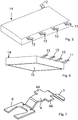
- Fig. 5 shows the housing 14 of the completely pressed power semiconductor module in plan view.
- the connection lugs 11, 12, 13 are led out laterally from the housing.
- the connections of the connection lugs 11, 12, 13 are on the side of the housing 14 opposite the substrate 9, so that the component can easily be soldered onto a circuit board, for example using SMD technology.
- Fig. 6 shows the same component from the underside, wherein the flat DCB surface 15 on the underside of the housing can be pressed against a heat sink for improved heat dissipation.
- the connection lugs are led out on the top of the housing.
- the Figures 7 to 9 show an alternative embodiment of the contact element 1, which differs from that with reference to FIG Figures 1 and 2
- the contact element described differs in that its first extension 5 is flat and its second extension 6 is mouth-shaped.
- the corresponding sections are provided with the same reference symbols.
- a mouth-shaped projection 6 prevents movement of the projection of the adjacent contact element transversely to the longitudinal direction of the contact element.
- the mouth-shaped extension 6 has an outwardly tapering cutout 6A, so that an offset is joined together
- Contact elements is also avoided in the longitudinal direction.
- the first attachment 5 has rounded corners, the contour of which corresponds to the contour of the inner section of the cutout 6A of the second attachment 6.
- the first extension 5 of one contact element 1 fits exactly into the second extension 6 of the other contact element 1. With the larger contact surface of the first extension 5, the contact with the substrate 9 is further improved.
- FIG. 9 shows that the first flat projection 5 of the contact element 1 is set lower than the second plate-shaped projection 6, ie the distance between the first projection 5 and the connecting piece 4 is greater than the distance between the second projection 6 and the connecting piece 8. Differences in height on the substrate 9 can thus be compensated for.
- Fig. 10 shows a possible application of the contact element 1 of FIG Figures 7 to 9 for contacting the diodes 8 on the plus side of the substrate 9, the lower-lying approach 5 of the contact elements 1 resting on the lower-lying contact surface of the metallization 10 and the higher-lying approach 6 resting on the higher-lying contact surface of the diode (chip) 8.
- the contact element 1 ′′ On the minus side of the substrate 9 there is a similar application for the contact element 1 ′′, which electrically connects one of the diodes 8 to the external connection lug 11.
- the contact element 1 ′′ in contrast to the exemplary embodiment from FIG Fig. 3 to a landing point on the connection tab 11 that is level with the contact surface of the chip can be avoided.
- the lower-lying projection 5 of the contact element 1 allows contact to be made on the wide flat contact surface of the substrate 9, which also saves a solder preform.
Landscapes
- Engineering & Computer Science (AREA)
- Microelectronics & Electronic Packaging (AREA)
- Power Engineering (AREA)
- Computer Hardware Design (AREA)
- Physics & Mathematics (AREA)
- Condensed Matter Physics & Semiconductors (AREA)
- General Physics & Mathematics (AREA)
- Chemical & Material Sciences (AREA)
- Ceramic Engineering (AREA)
- Materials Engineering (AREA)
- Structures For Mounting Electric Components On Printed Circuit Boards (AREA)
Description
Die Erfindung betrifft ein Leistungshalbleitermodul mit einem elektrische Kontaktflächen aufweisenden Träger, mindestens einem auf dem Träger angeordneten Leistungshalbleiterbauteil und mindestens zwei Kontaktelementen, die jeweils einen ersten und einen zweiten Ansatz aufweisen, die elektrisch mit einer Kontaktfläche des mindestens einen Leistungshalbleiterbauteils oder einer Kontaktfläche des Trägers verbunden sind. Die Erfindung bezieht sich insbesondere auf Halbleitermodule für höhere Leistungsanforderungen mit Dauergrenzströmen, die über 1 Ampere liegen können, wobei die aktiven Halbleiterchips und ggf. passiven Schaltungselemente sowie die internen wie externen Verbindungen auf flache, elektrisch isolierende Träger (Substrate) mittels Weichlöttechnik oder anderer geeigneter Verfahren aufgebracht werden, um elektrische Schaltungen zur Strom- und Spannungssteuerung bereit zu stellen.The invention relates to a power semiconductor module with a carrier having electrical contact areas, at least one power semiconductor component arranged on the carrier and at least two contact elements, each having a first and a second attachment, which are electrically connected to a contact area of the at least one power semiconductor component or a contact area of the carrier . The invention relates in particular to semiconductor modules for higher power requirements with continuous limit currents that can be above 1 ampere, the active semiconductor chips and possibly passive circuit elements as well as the internal and external connections on flat, electrically insulating carriers (substrates) by means of soft soldering or other suitable methods can be applied to provide electrical circuits for current and voltage control.
Zu den bekannten Verfahren zur Kontaktierung von Halbleiterchips gehören beispielsweise Ultraschall-Schweißverfahren, bei denen Aluminium-Bonddrahtverbindungen mittels Ultraschallschweißen hergestellt werden. Anstelle von Aluminiumdrähten können auch Kupferbänder Anwendung finden (
Alternativ sind schon seit langem Metallbügel bekannt, die vielfach aus Kupfer bestehen, das zur Verbesserung der Lötfähigkeit meist vernickelt ist. Diese sogenannten Clips werden mittels Weichlöttechnik und Lötformen montiert. Lötformen sind aber aufwendig herzustellen und für die Massenproduktion wegen manueller Bestückung weniger geeignet. Es sind auch lötformfreie Konstruktionen bekannt. Diese sind aber entweder nur für größere Bauteile verwendbar oder bei der Bestückung und während des Lötvorgangs schwierig in der nötigen Präzision zu handhaben.Alternatively, metal brackets have long been known, many of which are made of copper, which is usually nickel-plated to improve solderability. These so-called clips are mounted using soft soldering technology and soldering molds. However, soldering forms are complex and less suitable for mass production due to manual assembly. There are also known solder-free constructions. However, these can either only be used for larger components or difficult to handle with the necessary precision during assembly and during the soldering process.
Die
Die sogenannte "Clip"-Technik hat sich in der Praxis nicht als vorteilhaft erwiesen, wenn sehr dichte Anordnungen, beispielsweise Reihenschaltungen, auf Substraten realisiert werden müssen, die gleichzeitig noch über eine ausreichende Stromtragfähigkeit verfügen sollen.The so-called "clip" technique has not proven to be advantageous in practice when very dense arrangements, for example series connections, have to be implemented on substrates which at the same time should still have sufficient current carrying capacity.
Darüber hinaus sind auch Lösungen mit stumpf ausgestalteten Clip-Enden bekannt, um platzsparende Anordnungen zu schaffen (
Die
Der Erfindung liegt die Aufgabe zugrunde, die Nachteile der bekannten Kontaktierungsverfahren zu vermeiden und Kontaktelemente zu schaffen, die sowohl automatisiert verarbeitet werden können als auch bei dichter Bestückung auf Substraten den notwendigen Anforderungen an leichte Handhabbarkeit, große Zuverlässigkeit und hohe Stromtragfähigkeit genügen.The invention is based on the object of avoiding the disadvantages of the known contacting methods and of creating contact elements that can both be processed automatically and also meet the necessary requirements for easy handling, great reliability and high current-carrying capacity when densely populated on substrates.
Die Lösung dieser Aufgabe erfolgt mit den Merkmalen des Anspruchs 1. Die abhängigen Ansprüche betreffen vorteilhafte Ausführungsformen der Erfindung.This object is achieved with the features of
Das erfindungsgemäße Leistungshalbleitermodul verfügt über einen elektrische Kontaktflächen aufweisenden Träger, mindestens ein auf dem Träger angeordnetes Leistungshalbleiterbauteil und mindestens zwei Kontaktelemente.The power semiconductor module according to the invention has a carrier having electrical contact areas, at least one power semiconductor component arranged on the carrier, and at least two contact elements.
Die mindestens zwei erfindungsgemäßen Kontaktelemente weisen jeweils einen ersten und einen zweiten Ansatz auf, die elektrisch mit einer Kontaktfläche des mindestens einen Leistungshalbleiterbauteils oder einer Kontaktfläche des Trägers verbunden sind. Die Kontaktelemente können für sämtliche interne und externe Verbindungen zur Kontaktierung von aktiven Halbleiterchips und passiven Schaltungselementen dienen.The at least two contact elements according to the invention each have a first and a second attachment, which are electrically connected to a contact surface of the at least one power semiconductor component or a contact surface of the carrier. The contact elements can be used for all internal and external connections for contacting active semiconductor chips and passive circuit elements.
Jedes Kontaktelement weist ein langgestrecktes Verbindungsstück auf, an dessen Enden der erste und zweite Ansatz vorgesehen ist. Das langgestreckte Verbindungsstück mit dem ersten und zweiten Ansatz ist als ein flaches, gebogenes Metallstück ausgebildet.Each contact element has an elongated connecting piece, at the ends of which the first and second extensions are provided. The elongated connecting piece with the first and second extensions is designed as a flat, bent piece of metal.
Die Kontaktelemente sind derart auf dem Träger angeordnet und die Ansätze der Kontaktelemente sind derart ausgebildet, dass an einer Kontaktfläche des Leistungshalbleiterbauteils oder des Trägers der erste Ansatz des einen Kontaktelements von dem zweiten Ansatz des anderen Kontaktelements umfangsmäßig zumindest teilweise umschlossen wird. Dadurch wird eine besonders platzsparende elektrische Verbindung von jeweils zwei Kontaktelementen mit einer Kontaktstelle des Leistungshalbleiterbauteils oder des Trägers geschaffen, wobei die elektrische Verbindung mittels Weichlöten hergestellt werden kann. Anstelle einer Weichlötung kann für die elektrische Verbindung auch ein Ultraschall-Schweißverfahren eingesetzt werden. Aus der Anordnung der beiden Enden der Kontaktelemente in dichter Nachbarschaft ergibt sich eine hohe Stromtragfähigkeit. Die Handhabbarkeit wird dadurch vereinfacht, dass sich die Enden der Kontaktelemente vor der Herstellung der elektrischen Verbindung selbst justieren, in dem das eine Ende des einen Kontaktelements einen Anschlag für das andere Ende des anderen Kontaktelements bildet, da das eine Ende von dem anderen Ende zumindest teilweise umschlossen wird. Die Ansätze der Kontaktelemente sind mit der jeweiligen Kontaktfläche der strukturierten Metallisierung oder des Chips vorzugsweise verlötet. Bei einer Lötverbindung wird eine weitere Lot-Preform vermieden, die man sonst bei einer Überlappung der beiden Enden der Kontaktelemente benötigen würde.The contact elements are arranged on the carrier and the shoulders of the contact elements are designed such that the first extension of one contact element is at least partially circumferentially surrounded by the second extension of the other contact element on a contact surface of the power semiconductor component or of the carrier. This creates a particularly space-saving electrical connection between two contact elements and a contact point of the power semiconductor component or of the carrier, with the electrical connection being able to be established by means of soft soldering. Instead of soft soldering, an ultrasonic welding process can also be used for the electrical connection. From the arrangement of the two Ends of the contact elements in close proximity results in a high current carrying capacity. The handling is simplified in that the ends of the contact elements adjust themselves before the electrical connection is established, in that one end of one contact element forms a stop for the other end of the other contact element, since one end at least partially separates from the other end is enclosed. The approaches of the contact elements are preferably soldered to the respective contact surface of the structured metallization or the chip. With a soldered connection, another solder preform is avoided, which would otherwise be required if the two ends of the contact elements overlap.
Die jeweiligen Ansätze des Kontaktelement-Paars können unterschiedlich ausgebildet sein, solange der Ansatz des einen Kontaktelements von dem Ansatz des anderen Kontaktelements zumindest teilweise umschlossen wird.The respective approaches of the contact element pair can be designed differently as long as the approach of one contact element is at least partially enclosed by the approach of the other contact element.
Der erste und der zweite Ansatz sind an das langgestreckte Verbindungsstück nach einer Seite vorspringend angeformt sind, so dass zwischen dem Substrat und dem Verbindungsstück ein Abstand ist. Die gekröpften Ansätze erlauben die Überbrückung von bestimmten Bereichen auf dem Substrat.The first and the second approach are integrally formed on the elongated connecting piece so as to project to one side, so that there is a distance between the substrate and the connecting piece. The cranked approaches allow certain areas on the substrate to be bridged.
Eine Ausführungsform der Erfindung sieht vor, dass die Ansätze der Kontaktelemente derart ausgebildet sind, dass der erste Ansatz des einen Kontaktelements in dem zweiten Ansatz des anderen Kontaktelements quer zur Längsrichtung des Kontaktelements seitlich fixiert ist. Damit ist sichergestellt, dass die Kontaktelemente bei der Montage nicht seitlich zueinander versetzt werden können, sondern auf einer Linie liegen. Zum Ausgleich von Bauteiltoleranzen sollte aber auch hier ein gewisses Spiel vorhanden sein. In Längsrichtung des Kontaktelements kann der erste Ansatz des einen Kontaktelements in dem zweiten Ansatz des zweiten Kontaktelements lose geführt sein, so dass sich die Kontaktelemente in Längsrichtung ausrichten lassen.One embodiment of the invention provides that the shoulders of the contact elements are designed such that the first extension of one contact element is laterally fixed in the second extension of the other contact element transversely to the longitudinal direction of the contact element. This ensures that the contact elements cannot be offset laterally to one another during assembly, but rather lie on a line. To compensate for component tolerances, there should also be a certain amount of play here. In the longitudinal direction of the contact element, the first extension of one contact element can be guided loosely in the second extension of the second contact element, so that the contact elements can be aligned in the longitudinal direction.
Bei einer bevorzugten Ausführungsform ist das langgestreckte Verbindungsstück mit dem ersten und zweiten Ansatz mit Weichlot beschichtet, so dass die Herstellung der elektrischen Verbindung vereinfacht wird.In a preferred embodiment, the elongated connecting piece with the first and second extensions is coated with soft solder, so that the production of the electrical connection is simplified.
Der erste Ansatz des Kontaktelements kann einen U-förmigen Querschnitt aufweisen. Der erste Ansatz kann aber anders ausgebildet sein. Entscheidend ist nur, dass er in den zweiten Ansatz des anderen Kontaktelements ohne zu Verklemmen passend eingesetzt werden kann.The first approach of the contact element can have a U-shaped cross section. The first approach can, however, be designed differently. The only decisive factor is that it can be used appropriately in the second approach of the other contact element without jamming.
Der zweite Ansatz des Kontaktelements ist vorzugsweise ein plattenförmiger oder tellerförmiger Ansatz, der flach auf der Kontaktfläche aufliegt und eine Ausnehmung aufweist, die den ersten Ansatz des anderen Kontaktelements aufnimmt. Vorzugsweise ist die Ausnehmung des zweiten Ansatzes eine rechteckförmige Ausnehmung. Die Ausnehmung kann aber auch beispielsweise rund oder oval sein. Eine runde Ausnehmung erlaubt die Anordnung der Kontaktelemente nicht nur auf einer Linie, sondern in einem weiten Winkelbereich zueinander. Beispielsweise können die benachbarten Kontaktelemente einen rechten Winkel einschließen.The second extension of the contact element is preferably a plate-shaped or plate-shaped extension which rests flat on the contact surface and has a recess which receives the first extension of the other contact element. The recess of the second attachment is preferably a rectangular recess. The recess can also be round or oval, for example. A round recess allows the contact elements to be arranged not just on a line, but in one wide angular range to each other. For example, the adjacent contact elements can enclose a right angle.
Bei einer weiteren Ausführungsform ist der zweite Ansatz des Kontaktelements in der Art eines Mauls ausgebildet, das den ersten Ansatz des anderen Kontaktelements seitlich umschließt. Der maulförmige Ansatz kann einen sich nach außen verjüngenden Ausschnitt aufweisen, der den ersten Ansatz auch in Längsrichtung fixiert.In a further embodiment, the second extension of the contact element is designed in the manner of a mouth which laterally encloses the first extension of the other contact element. The mouth-shaped extension can have an outwardly tapering cutout which also fixes the first extension in the longitudinal direction.
Der Kontaktflächen aufweisende Träger kann unterschiedlich ausgebildet sein. Vorzugsweise ist der Träger ein Substrat, das an mindestens einer Seite eine metallische Strukturierung aufweist, insbesondere ein beidseitig metallisiertes Keramiksubstrat, das in der DCB-Technik hergestellt sein kann. Der Träger kann aber auch ein metallischer Träger sein, der nicht über eine strukturierte Metallisierung verfügt, sondern zur Schaffung der Kontaktflächen gestanzt ist.The carrier having contact surfaces can be designed differently. The carrier is preferably a substrate which has a metallic structure on at least one side, in particular a ceramic substrate which is metallized on both sides and which can be produced using DCB technology. The carrier can, however, also be a metallic carrier that does not have a structured metallization but is punched to create the contact surfaces.
Das Leitungshalbleitermodul kann ein den Träger zumindest teilweise umschließendes Gehäuse aufweisen, aus dem Anschlüsse, beispielsweise Leistungs- und/oder Steueranschlüsse, herausgeführt sind, die mit einer Kontaktfläche des mindestens einen Leistungshalbleiterbauteils oder des Trägers elektrisch verbunden sind. Die erfindungsgemäßen Kontaktelemente können auch die seitlichen Anschlüsse bilden.The line semiconductor module can have a housing which at least partially encloses the carrier, from which connections, for example power and / or control connections, are led out, which are electrically connected to a contact surface of the at least one power semiconductor component or of the carrier. The contact elements according to the invention can also form the lateral connections.
Nachfolgend werden unter Bezugnahme auf die Zeichnungen Ausführungsbeispiele des erfindungsgemäßen Leistungshalbleitermoduls näher beschrieben.Embodiments of the power semiconductor module according to the invention are described in more detail below with reference to the drawings.
Es zeigen:
- Fig. 1
- das erfindungsgemäße Kontaktelement des erfindungsgemäßen Leistungshalbleitermoduls in der Draufsicht,
- Fig. 2
- einen Schnitt durch das Kontaktelement von
Fig. 1 , - Fig. 3
- der die Leistungshalbleiter tragende Träger des erfindungsgemäßen Leistungshalbleitermoduls, wobei die serielle Verschaltung mehrerer Leistungshalbleiter mit den erfindungsgemäßen Kontaktelementen gezeigt ist,
- Fig. 4
- einen Ausschnitt von
Fig. 3 in vergrößerter Darstellung, - Fig. 5
- das in einem Gehäuse gekapselte Leistungshalbleitermodul in der Draufsicht,
- Fig. 6
- das Leistungshalbleitermodul von
Fig. 5 in der Unteransicht, - Fig. 7
- eine alternative Ausführungsform des erfindungsgemäßen Kontaktelements mit einem maulförmigen Ansatz,
- Fig. 8
- das Kontaktelement von
Fig. 7 in der Draufsicht, - Fig. 9
- einen Schnitt durch das Kontaktelement von
Fig. 7 und - Fig. 10
- der Träger mit den Leistungshalbleitern und den Kontaktelementen eines weiteren Ausführungsbeispiels des erfindungsgemäßen Leistungshalbleitermoduls.
- Fig. 1
- the contact element according to the invention of the power semiconductor module according to the invention in plan view,
- Fig. 2
- a section through the contact element of
Fig. 1 , - Fig. 3
- the carrier of the power semiconductor module according to the invention carrying the power semiconductors, the serial interconnection of several power semiconductors with the contact elements according to the invention being shown,
- Fig. 4
- a section of
Fig. 3 in an enlarged view, - Fig. 5
- the power semiconductor module encapsulated in a housing in plan view,
- Fig. 6
- the power semiconductor module from
Fig. 5 in the bottom view, - Fig. 7
- an alternative embodiment of the contact element according to the invention with a mouth-shaped approach,
- Fig. 8
- the contact element of
Fig. 7 in plan view, - Fig. 9
- a section through the contact element of
Fig. 7 and - Fig. 10
- the carrier with the power semiconductors and the contact elements of a further exemplary embodiment of the power semiconductor module according to the invention.
Die
Das Kontaktelement 1 weist eine dem in den
Das gebogene Metallstück des Kontaktelements 1 weist ein langgestrecktes, bogenförmiges Verbindungsstück 4 auf, an dessen in den
Der erste Ansatz 5 ist bei dem vorliegenden Ausführungsbeispiel hakenförmig ausgebildet. Er kann aber auch plattenförmig oder stumpf sein. Bei dem vorliegenden Ausführungsbeispiel hat der erste Ansatz 5 einen U-förmigen Querschnitt, um mit einer lotfähigen Chipoberfläche kontaktiert werden zu können. Der erste Ansatz 5 kann auch flacher ausgebildet sein, um für eine Weichlötung eine größere Kontaktfläche zu schaffen.In the present exemplary embodiment, the
Der zweite Ansatz 6 ist plattenförmig ausgebildet, wobei in dem plattenförmigen Ansatz 6 eine Ausnehmung 7 vorgesehen ist. Die Ausnehmung 7 ist bei dem vorliegenden Ausführungsbeispiel rechteckförmig. Die Breite des ersten Ansatzes 5 entspricht der Breite der Ausnehmung 7 des zweiten Ansatzes 6, so dass der erste Ansatz 5 eines Kontaktelements 1 in den zweiten Ansatz 6 eines anderen Kontaktelements 1 passend eingesetzt werden kann. Dabei sollte der erste Ansatz 5 in dem zweiten Ansatz 6 unter Berücksichtigung möglicher Toleranzen ein gewisses Spiel haben, so dass er nicht verklemmen kann.The
Das erfindungsgemäße Leistungshalbleitermodul verfügt über mindestens zwei gleiche oder gleichartige Kontaktelemente 1, die sich durch die besondere Ausbildung der Ansätze 5, 6 auszeichnen. Die
Als Träger 9 dient eine beidseitig mittels DCB-Technik (Direct Copper Bonding) metallisierte Keramikplatte, beispielsweise aus Aluminiumoxid, deren Oberseite entsprechend dem erforderlichen Schaltungsmuster strukturiert ist. Die
Auf der Seite der Wechselspannungseingänge sind mehrere Kontaktelemente 1, 1', 1" in einer Reihe angeordnet, um den Minus-Pol der Brücke herzustellen. Dabei sitzt der erste Ansatz 5 des einen Kontaktelements 1 exakt in der Ausnehmung 7 des zweiten Ansatzes 6 des benachbarten Kontaktelements 1. Der plattenförmige Ansatz 6 des ersten Kontaktelements 1 kontaktiert die obere Kontaktfläche der ersten Diode 8 und der hakenförmige Ansatz 5 des ersten Kontaktelements 1 sitzt in der Ausnehmung 7 des plattenförmigen Ansatzes 6 des zweiten Kontaktelements 1', das die Kontaktfläche der zweiten Diode 8 kontaktiert. Der hakenförmige Ansatz 5 des zweiten Kontaktelements 1' sitzt wiederum in der Ausnehmung 7 des plattenförmigen Ansatzes 6 des dritten Kontaktelements 1", das die Oberseite der dritten Diode 8 kontaktiert. Dabei ist der hakenförmige Ansatz 5 des dritten Kontaktelements 1" elektrisch mit einer externen Anschlusslasche 11 für den Minus-Pol verbunden. Mit gleichartigen Kontaktelementen 1 werden auch weitere elektrische Verbindungen zu den anderen Dioden 8 hergestellt, wobei die Kontaktelemente aber nicht in einer Reihe angeordnet sind. Das Halbleitermodul verfügt noch über eine externe Anschlusslasche 12 für den Plus-Pol und weitere externe Anschlusslaschen 13 für die Wechselspannungsanschlüsse, die aus dem in den
Die Anordnung und Ausbildung der Kontaktelemente 1 hat den Vorteil, dass sie platzsparend ist und gleichzeitig eine maximale Stromtragfähigkeit aufweist. Die Abstände zwischen den inneren Randbereichen der jeweils benachbarten Ansätze 5, 6 der Kontaktelemente 1 sind an der Verbindungsstelle sehr klein, was zu minimalen Übergangswiderständen führt. Darüber hinaus ist die Kontaktfläche zu den rechteckigen Chips durch die plattenförmigen vorzugsweise ebenfalls rechteckförmigen Ansätze 6 der Kontaktelemente 1 optimal ausgenutzt.The arrangement and design of the
Das Substrat 9 mit den Halbleiterbauelementen 8 und Kontaktelementen 1 wird im Allgemeinen mittels Umpresstechnik verkapselt und die in Kammtechnik angebrachten Außenanschlüsse anschließend getrennt, was beispielsweise in der
Die
Die Schnittdarstellung von
Claims (12)
- A power semiconductor module comprising a support (9) with electric contact surfaces, at least one power semiconductor component (8) located on the support (9) and at least two contact elements (1, 1', 1"), which each have a first and a second lug (5, 6), which are electrically connected to a contact surface of the at least one power semiconductor component (8) or to a contact surface of the support (9),
characterised in that the at least two contact elements (1) have an elongated connecting portion (4) at the ends of which the first and the second lug (5, 6) are provided,
in that the elongated connecting portion (4) with the first and second lugs (5, 6) is designed as a flat, bent metal piece, wherein the lugs (5, 6) of the at least two contact elements (1, 1', 1") are designed such that on one contact surface of the power semiconductor component (8) or of the support (9) the first lug (5) of the one contact element (1; 1') is at least partially surrounded around the circumference by the second lug (6) of the other contact element (1'; 1"), and
in that the first and second lugs (5, 6) are shaped onto the elongated connecting portion (4) so that they protrude to one side. - The power semiconductor module according to claim 1, characterised in that the lugs (5, 6) of the at least two contact elements (1, 1', 1") are designed such that the first lug (5) of the one contact element (1; 1') is fixed laterally into the second lug (6) of the other contact element (1'; 1") crosswise to the longitudinal direction of the at least two contact elements (1, 1', 1").
- The power semiconductor module according to claim 1 or 2, characterised in that the lugs (5, 6) of the at least two contact elements (1, 1', 1") are designed such that the first lug (5) of the one contact element (1; 1') is loosely positioned into the second lug (6) of the other contact element (1'; 1") in the longitudinal direction of the at least two contact elements (1, 1', 1").
- The power semiconductor module according to one of claims 1 to 3, characterised in that the elongated connecting portion (4) with the first and second lugs (5, 6) is coated with soft solder.
- The power semiconductor module according to one of claims 1 to 4, characterised in that the first lug (5) of the at least two contact elements (1, 1', 1") has a U-shaped cross-section.
- The power semiconductor module according to one of claims 1 to 5, characterised in that the second lug (6) of the at least two contact elements (1, 1', 1") is a plate-shaped or dishshaped lug with a recess (7).
- The power semiconductor module according to claim 6, characterised in that the recess (7) of the second lug (6) is a rectangular recess.
- The power semiconductor module according to claim 6 or 7, characterised in that the second lug (6) of the at least two contact elements (1, 1', 1") is designed in the form of a jaw.
- The power semiconductor module according to one of claims 1 to 8, characterised in that the lugs (5, 6) of the at least two contact elements (1, 1', 1") are soldered to the contact surface of the power semiconductor (8) or of the support (9).
- The power semiconductor module according to one of claims 1 to 9, characterised in that the support is a substrate (9) which has a structured metal plating (10) on at least one side, and in particular is a ceramic substrate with metal plating on both sides.
- The power semiconductor module according to one of claims 1 to 10, characterised in that the support (9) is a punched metallic support.
- The power semiconductor module according to one of claims 1 to 11, characterised in that the power semiconductor module has a housing (14) surrounding the support (9) at least in part, out of which housing connections (11, 12, 13) are routed which are electrically connected to a contact surface of the at least one power semiconductor component (8) or a contact surface of the support.
Priority Applications (1)
| Application Number | Priority Date | Filing Date | Title |
|---|---|---|---|
| EP14164812.1A EP2933836B1 (en) | 2014-04-15 | 2014-04-15 | Power semiconductor module |
Applications Claiming Priority (1)
| Application Number | Priority Date | Filing Date | Title |
|---|---|---|---|
| EP14164812.1A EP2933836B1 (en) | 2014-04-15 | 2014-04-15 | Power semiconductor module |
Publications (2)
| Publication Number | Publication Date |
|---|---|
| EP2933836A1 EP2933836A1 (en) | 2015-10-21 |
| EP2933836B1 true EP2933836B1 (en) | 2020-10-14 |
Family
ID=50543442
Family Applications (1)
| Application Number | Title | Priority Date | Filing Date |
|---|---|---|---|
| EP14164812.1A Active EP2933836B1 (en) | 2014-04-15 | 2014-04-15 | Power semiconductor module |
Country Status (1)
| Country | Link |
|---|---|
| EP (1) | EP2933836B1 (en) |
Families Citing this family (1)
| Publication number | Priority date | Publication date | Assignee | Title |
|---|---|---|---|---|
| DE102021206587A1 (en) | 2021-06-25 | 2022-12-29 | Robert Bosch Gesellschaft mit beschränkter Haftung | Electrical arrangement with positioning aid and manufacturing method |
Family Cites Families (8)
| Publication number | Priority date | Publication date | Assignee | Title |
|---|---|---|---|---|
| DE3406538A1 (en) | 1984-02-23 | 1985-08-29 | Bbc Brown Boveri & Cie | PERFORMANCE SEMICONDUCTOR MODULE AND PRODUCTION METHOD |
| DE10103084B4 (en) | 2001-01-24 | 2006-08-03 | Infineon Technologies Ag | Semiconductor module and method for its production |
| DE10316355C5 (en) | 2003-04-10 | 2008-03-06 | Semikron Elektronik Gmbh & Co. Kg | Power semiconductor module with flexible external pin assignment |
| DE102005016650B4 (en) * | 2005-04-12 | 2009-11-19 | Semikron Elektronik Gmbh & Co. Kg | Power semiconductor module with butt soldered connection and connection elements |
| DE102005045100A1 (en) | 2005-09-21 | 2007-03-29 | Infineon Technologies Ag | Method for producing a power semiconductor module |
| JP4455488B2 (en) * | 2005-12-19 | 2010-04-21 | 三菱電機株式会社 | Semiconductor device |
| DE102007014789B3 (en) | 2007-03-28 | 2008-11-06 | Ixys Ch Gmbh | Arrangement of at least one power semiconductor module and a printed circuit board and power semiconductor module |
| KR101278393B1 (en) * | 2010-11-01 | 2013-06-24 | 삼성전기주식회사 | Power package module and a fabricating mothod the same |
-
2014
- 2014-04-15 EP EP14164812.1A patent/EP2933836B1/en active Active
Non-Patent Citations (1)
| Title |
|---|
| None * |
Also Published As
| Publication number | Publication date |
|---|---|
| EP2933836A1 (en) | 2015-10-21 |
Similar Documents
| Publication | Publication Date | Title |
|---|---|---|
| DE102014202651B4 (en) | Semiconductor devices and semiconductor module | |
| EP3262666B1 (en) | Electrical element and method for manufacturing it | |
| DE112013001612B4 (en) | Semiconductor component and method for its manufacture | |
| DE102011082781B4 (en) | SEMICONDUCTOR DEVICE WITH A PLATE ELECTRODE FOR CONNECTING A MULTIPLE OF SEMICONDUCTOR CHIPS | |
| DE3913221A1 (en) | SEMICONDUCTOR ARRANGEMENT | |
| DE102015122259B4 (en) | Semiconductor devices having a porous insulating layer | |
| DE102016112289B4 (en) | Lead frame and method of making the same | |
| DE102012105929A1 (en) | Semiconductor device with a contact clip with projections and manufacture thereof | |
| DE102013100701B4 (en) | SEMICONDUCTOR MODULE ARRANGEMENT AND METHOD FOR MANUFACTURING A SEMICONDUCTOR MODULE ARRANGEMENT | |
| DE102014104399B4 (en) | Semiconductor chip package comprising a leadframe | |
| WO2004109812A2 (en) | Housing for a radiation-emitting component, method for the production thereof, and radiation-emitting component | |
| DE102011113269A1 (en) | Semiconductor module and method for its production | |
| DE102019112935B4 (en) | Semiconductor module | |
| DE102008035911A1 (en) | Method for manufacturing an integrated circuit module | |
| DE4207198A1 (en) | FEEDER FRAME AND SEMICONDUCTOR DEVICE USING THE FEEDER FRAME | |
| DE102009047555A1 (en) | Low height electrical connector | |
| DE102014223863B4 (en) | power semiconductor devices | |
| DE102018206482B4 (en) | Semiconductor component with a composite clip made of composite material | |
| DE102020105267A1 (en) | Semiconductor device and method of manufacturing the same | |
| DE10205698A1 (en) | Light-emitting diode has electrical wirings formed on surface of insulated cup for electrical connection to LED chip stored in insulated cup | |
| DE102015223300B4 (en) | semiconductor device | |
| EP3619739B1 (en) | Semiconductor module | |
| EP2933836B1 (en) | Power semiconductor module | |
| DE112020002845T5 (en) | SEMICONDUCTOR DEVICE | |
| DE4300516C2 (en) | Power semiconductor module |
Legal Events
| Date | Code | Title | Description |
|---|---|---|---|
| PUAI | Public reference made under article 153(3) epc to a published international application that has entered the european phase |
Free format text: ORIGINAL CODE: 0009012 |
|
| AK | Designated contracting states |
Kind code of ref document: A1 Designated state(s): AL AT BE BG CH CY CZ DE DK EE ES FI FR GB GR HR HU IE IS IT LI LT LU LV MC MK MT NL NO PL PT RO RS SE SI SK SM TR |
|
| AX | Request for extension of the european patent |
Extension state: BA ME |
|
| 17P | Request for examination filed |
Effective date: 20160408 |
|
| RBV | Designated contracting states (corrected) |
Designated state(s): AL AT BE BG CH CY CZ DE DK EE ES FI FR GB GR HR HU IE IS IT LI LT LU LV MC MK MT NL NO PL PT RO RS SE SI SK SM TR |
|
| STAA | Information on the status of an ep patent application or granted ep patent |
Free format text: STATUS: EXAMINATION IS IN PROGRESS |
|
| 17Q | First examination report despatched |
Effective date: 20190919 |
|
| GRAP | Despatch of communication of intention to grant a patent |
Free format text: ORIGINAL CODE: EPIDOSNIGR1 |
|
| STAA | Information on the status of an ep patent application or granted ep patent |
Free format text: STATUS: GRANT OF PATENT IS INTENDED |
|
| INTG | Intention to grant announced |
Effective date: 20200507 |
|
| GRAS | Grant fee paid |
Free format text: ORIGINAL CODE: EPIDOSNIGR3 |
|
| GRAA | (expected) grant |
Free format text: ORIGINAL CODE: 0009210 |
|
| STAA | Information on the status of an ep patent application or granted ep patent |
Free format text: STATUS: THE PATENT HAS BEEN GRANTED |
|
| AK | Designated contracting states |
Kind code of ref document: B1 Designated state(s): AL AT BE BG CH CY CZ DE DK EE ES FI FR GB GR HR HU IE IS IT LI LT LU LV MC MK MT NL NO PL PT RO RS SE SI SK SM TR |
|
| REG | Reference to a national code |
Ref country code: GB Ref legal event code: FG4D Free format text: NOT ENGLISH |
|
| REG | Reference to a national code |
Ref country code: AT Ref legal event code: REF Ref document number: 1324416 Country of ref document: AT Kind code of ref document: T Effective date: 20201015 Ref country code: CH Ref legal event code: EP |
|
| REG | Reference to a national code |
Ref country code: DE Ref legal event code: R096 Ref document number: 502014014875 Country of ref document: DE |
|
| REG | Reference to a national code |
Ref country code: IE Ref legal event code: FG4D Free format text: LANGUAGE OF EP DOCUMENT: GERMAN |
|
| REG | Reference to a national code |
Ref country code: NL Ref legal event code: MP Effective date: 20201014 |
|
| PG25 | Lapsed in a contracting state [announced via postgrant information from national office to epo] |
Ref country code: GR Free format text: LAPSE BECAUSE OF FAILURE TO SUBMIT A TRANSLATION OF THE DESCRIPTION OR TO PAY THE FEE WITHIN THE PRESCRIBED TIME-LIMIT Effective date: 20210115 Ref country code: FI Free format text: LAPSE BECAUSE OF FAILURE TO SUBMIT A TRANSLATION OF THE DESCRIPTION OR TO PAY THE FEE WITHIN THE PRESCRIBED TIME-LIMIT Effective date: 20201014 Ref country code: RS Free format text: LAPSE BECAUSE OF FAILURE TO SUBMIT A TRANSLATION OF THE DESCRIPTION OR TO PAY THE FEE WITHIN THE PRESCRIBED TIME-LIMIT Effective date: 20201014 Ref country code: NO Free format text: LAPSE BECAUSE OF FAILURE TO SUBMIT A TRANSLATION OF THE DESCRIPTION OR TO PAY THE FEE WITHIN THE PRESCRIBED TIME-LIMIT Effective date: 20210114 Ref country code: NL Free format text: LAPSE BECAUSE OF FAILURE TO SUBMIT A TRANSLATION OF THE DESCRIPTION OR TO PAY THE FEE WITHIN THE PRESCRIBED TIME-LIMIT Effective date: 20201014 Ref country code: PT Free format text: LAPSE BECAUSE OF FAILURE TO SUBMIT A TRANSLATION OF THE DESCRIPTION OR TO PAY THE FEE WITHIN THE PRESCRIBED TIME-LIMIT Effective date: 20210215 |
|
| REG | Reference to a national code |
Ref country code: LT Ref legal event code: MG4D |
|
| PG25 | Lapsed in a contracting state [announced via postgrant information from national office to epo] |
Ref country code: SE Free format text: LAPSE BECAUSE OF FAILURE TO SUBMIT A TRANSLATION OF THE DESCRIPTION OR TO PAY THE FEE WITHIN THE PRESCRIBED TIME-LIMIT Effective date: 20201014 Ref country code: LV Free format text: LAPSE BECAUSE OF FAILURE TO SUBMIT A TRANSLATION OF THE DESCRIPTION OR TO PAY THE FEE WITHIN THE PRESCRIBED TIME-LIMIT Effective date: 20201014 Ref country code: IS Free format text: LAPSE BECAUSE OF FAILURE TO SUBMIT A TRANSLATION OF THE DESCRIPTION OR TO PAY THE FEE WITHIN THE PRESCRIBED TIME-LIMIT Effective date: 20210214 Ref country code: PL Free format text: LAPSE BECAUSE OF FAILURE TO SUBMIT A TRANSLATION OF THE DESCRIPTION OR TO PAY THE FEE WITHIN THE PRESCRIBED TIME-LIMIT Effective date: 20201014 Ref country code: ES Free format text: LAPSE BECAUSE OF FAILURE TO SUBMIT A TRANSLATION OF THE DESCRIPTION OR TO PAY THE FEE WITHIN THE PRESCRIBED TIME-LIMIT Effective date: 20201014 Ref country code: BG Free format text: LAPSE BECAUSE OF FAILURE TO SUBMIT A TRANSLATION OF THE DESCRIPTION OR TO PAY THE FEE WITHIN THE PRESCRIBED TIME-LIMIT Effective date: 20210114 |
|
| PG25 | Lapsed in a contracting state [announced via postgrant information from national office to epo] |
Ref country code: HR Free format text: LAPSE BECAUSE OF FAILURE TO SUBMIT A TRANSLATION OF THE DESCRIPTION OR TO PAY THE FEE WITHIN THE PRESCRIBED TIME-LIMIT Effective date: 20201014 |
|
| REG | Reference to a national code |
Ref country code: DE Ref legal event code: R097 Ref document number: 502014014875 Country of ref document: DE |
|
| PG25 | Lapsed in a contracting state [announced via postgrant information from national office to epo] |
Ref country code: SK Free format text: LAPSE BECAUSE OF FAILURE TO SUBMIT A TRANSLATION OF THE DESCRIPTION OR TO PAY THE FEE WITHIN THE PRESCRIBED TIME-LIMIT Effective date: 20201014 Ref country code: RO Free format text: LAPSE BECAUSE OF FAILURE TO SUBMIT A TRANSLATION OF THE DESCRIPTION OR TO PAY THE FEE WITHIN THE PRESCRIBED TIME-LIMIT Effective date: 20201014 Ref country code: LT Free format text: LAPSE BECAUSE OF FAILURE TO SUBMIT A TRANSLATION OF THE DESCRIPTION OR TO PAY THE FEE WITHIN THE PRESCRIBED TIME-LIMIT Effective date: 20201014 Ref country code: EE Free format text: LAPSE BECAUSE OF FAILURE TO SUBMIT A TRANSLATION OF THE DESCRIPTION OR TO PAY THE FEE WITHIN THE PRESCRIBED TIME-LIMIT Effective date: 20201014 Ref country code: CZ Free format text: LAPSE BECAUSE OF FAILURE TO SUBMIT A TRANSLATION OF THE DESCRIPTION OR TO PAY THE FEE WITHIN THE PRESCRIBED TIME-LIMIT Effective date: 20201014 Ref country code: SM Free format text: LAPSE BECAUSE OF FAILURE TO SUBMIT A TRANSLATION OF THE DESCRIPTION OR TO PAY THE FEE WITHIN THE PRESCRIBED TIME-LIMIT Effective date: 20201014 |
|
| PLBE | No opposition filed within time limit |
Free format text: ORIGINAL CODE: 0009261 |
|
| STAA | Information on the status of an ep patent application or granted ep patent |
Free format text: STATUS: NO OPPOSITION FILED WITHIN TIME LIMIT |
|
| PG25 | Lapsed in a contracting state [announced via postgrant information from national office to epo] |
Ref country code: DK Free format text: LAPSE BECAUSE OF FAILURE TO SUBMIT A TRANSLATION OF THE DESCRIPTION OR TO PAY THE FEE WITHIN THE PRESCRIBED TIME-LIMIT Effective date: 20201014 |
|
| 26N | No opposition filed |
Effective date: 20210715 |
|
| PG25 | Lapsed in a contracting state [announced via postgrant information from national office to epo] |
Ref country code: AL Free format text: LAPSE BECAUSE OF FAILURE TO SUBMIT A TRANSLATION OF THE DESCRIPTION OR TO PAY THE FEE WITHIN THE PRESCRIBED TIME-LIMIT Effective date: 20201014 |
|
| PG25 | Lapsed in a contracting state [announced via postgrant information from national office to epo] |
Ref country code: SI Free format text: LAPSE BECAUSE OF FAILURE TO SUBMIT A TRANSLATION OF THE DESCRIPTION OR TO PAY THE FEE WITHIN THE PRESCRIBED TIME-LIMIT Effective date: 20201014 Ref country code: MC Free format text: LAPSE BECAUSE OF FAILURE TO SUBMIT A TRANSLATION OF THE DESCRIPTION OR TO PAY THE FEE WITHIN THE PRESCRIBED TIME-LIMIT Effective date: 20201014 |
|
| PG25 | Lapsed in a contracting state [announced via postgrant information from national office to epo] |
Ref country code: LU Free format text: LAPSE BECAUSE OF NON-PAYMENT OF DUE FEES Effective date: 20210415 |
|
| REG | Reference to a national code |
Ref country code: BE Ref legal event code: MM Effective date: 20210430 |
|
| PG25 | Lapsed in a contracting state [announced via postgrant information from national office to epo] |
Ref country code: LI Free format text: LAPSE BECAUSE OF NON-PAYMENT OF DUE FEES Effective date: 20210430 Ref country code: CH Free format text: LAPSE BECAUSE OF NON-PAYMENT OF DUE FEES Effective date: 20210430 |
|
| PG25 | Lapsed in a contracting state [announced via postgrant information from national office to epo] |
Ref country code: IE Free format text: LAPSE BECAUSE OF NON-PAYMENT OF DUE FEES Effective date: 20210415 |
|
| PG25 | Lapsed in a contracting state [announced via postgrant information from national office to epo] |
Ref country code: IS Free format text: LAPSE BECAUSE OF FAILURE TO SUBMIT A TRANSLATION OF THE DESCRIPTION OR TO PAY THE FEE WITHIN THE PRESCRIBED TIME-LIMIT Effective date: 20210214 |
|
| REG | Reference to a national code |
Ref country code: AT Ref legal event code: MM01 Ref document number: 1324416 Country of ref document: AT Kind code of ref document: T Effective date: 20210415 |
|
| PG25 | Lapsed in a contracting state [announced via postgrant information from national office to epo] |
Ref country code: BE Free format text: LAPSE BECAUSE OF NON-PAYMENT OF DUE FEES Effective date: 20210430 |
|
| PG25 | Lapsed in a contracting state [announced via postgrant information from national office to epo] |
Ref country code: AT Free format text: LAPSE BECAUSE OF NON-PAYMENT OF DUE FEES Effective date: 20210415 |
|
| PGFP | Annual fee paid to national office [announced via postgrant information from national office to epo] |
Ref country code: FR Payment date: 20230309 Year of fee payment: 10 |
|
| PG25 | Lapsed in a contracting state [announced via postgrant information from national office to epo] |
Ref country code: HU Free format text: LAPSE BECAUSE OF FAILURE TO SUBMIT A TRANSLATION OF THE DESCRIPTION OR TO PAY THE FEE WITHIN THE PRESCRIBED TIME-LIMIT; INVALID AB INITIO Effective date: 20140415 |
|
| PGFP | Annual fee paid to national office [announced via postgrant information from national office to epo] |
Ref country code: IT Payment date: 20230310 Year of fee payment: 10 |
|
| PG25 | Lapsed in a contracting state [announced via postgrant information from national office to epo] |
Ref country code: CY Free format text: LAPSE BECAUSE OF FAILURE TO SUBMIT A TRANSLATION OF THE DESCRIPTION OR TO PAY THE FEE WITHIN THE PRESCRIBED TIME-LIMIT Effective date: 20201014 |
|
| P01 | Opt-out of the competence of the unified patent court (upc) registered |
Effective date: 20230607 |
|
| PGFP | Annual fee paid to national office [announced via postgrant information from national office to epo] |
Ref country code: DE Payment date: 20230307 Year of fee payment: 10 |
|
| PG25 | Lapsed in a contracting state [announced via postgrant information from national office to epo] |
Ref country code: MK Free format text: LAPSE BECAUSE OF FAILURE TO SUBMIT A TRANSLATION OF THE DESCRIPTION OR TO PAY THE FEE WITHIN THE PRESCRIBED TIME-LIMIT Effective date: 20201014 |
|
| PGFP | Annual fee paid to national office [announced via postgrant information from national office to epo] |
Ref country code: GB Payment date: 20240229 Year of fee payment: 11 |