EP2907294B1 - Ear position and gesture detection with mobile device - Google Patents
Ear position and gesture detection with mobile device Download PDFInfo
- Publication number
- EP2907294B1 EP2907294B1 EP13779493.9A EP13779493A EP2907294B1 EP 2907294 B1 EP2907294 B1 EP 2907294B1 EP 13779493 A EP13779493 A EP 13779493A EP 2907294 B1 EP2907294 B1 EP 2907294B1
- Authority
- EP
- European Patent Office
- Prior art keywords
- ear
- array
- implementations
- cell phone
- voltage
- Prior art date
- Legal status (The legal status is an assumption and is not a legal conclusion. Google has not performed a legal analysis and makes no representation as to the accuracy of the status listed.)
- Active
Links
- 238000001514 detection method Methods 0.000 title description 6
- 238000000034 method Methods 0.000 claims description 109
- 239000010410 layer Substances 0.000 description 161
- 230000003287 optical effect Effects 0.000 description 51
- 230000008569 process Effects 0.000 description 50
- 238000010586 diagram Methods 0.000 description 26
- 239000000463 material Substances 0.000 description 23
- 239000000758 substrate Substances 0.000 description 18
- VYPSYNLAJGMNEJ-UHFFFAOYSA-N Silicium dioxide Chemical compound O=[Si]=O VYPSYNLAJGMNEJ-UHFFFAOYSA-N 0.000 description 13
- 230000008859 change Effects 0.000 description 12
- 238000000151 deposition Methods 0.000 description 11
- 230000006870 function Effects 0.000 description 9
- 238000003860 storage Methods 0.000 description 9
- 238000013475 authorization Methods 0.000 description 8
- 230000015572 biosynthetic process Effects 0.000 description 8
- 238000004519 manufacturing process Methods 0.000 description 8
- 238000000059 patterning Methods 0.000 description 8
- 239000006096 absorbing agent Substances 0.000 description 7
- 238000005530 etching Methods 0.000 description 7
- 229910052751 metal Inorganic materials 0.000 description 7
- 239000002184 metal Substances 0.000 description 7
- 238000013461 design Methods 0.000 description 6
- 230000033001 locomotion Effects 0.000 description 6
- 238000012545 processing Methods 0.000 description 6
- 239000000377 silicon dioxide Substances 0.000 description 6
- 230000008901 benefit Effects 0.000 description 5
- 230000001413 cellular effect Effects 0.000 description 5
- 230000003750 conditioning effect Effects 0.000 description 5
- 230000008021 deposition Effects 0.000 description 5
- 239000003990 capacitor Substances 0.000 description 4
- 238000004590 computer program Methods 0.000 description 4
- 238000000926 separation method Methods 0.000 description 4
- BLIQUJLAJXRXSG-UHFFFAOYSA-N 1-benzyl-3-(trifluoromethyl)pyrrolidin-1-ium-3-carboxylate Chemical compound C1C(C(=O)O)(C(F)(F)F)CCN1CC1=CC=CC=C1 BLIQUJLAJXRXSG-UHFFFAOYSA-N 0.000 description 3
- 229910000838 Al alloy Inorganic materials 0.000 description 3
- 229910052782 aluminium Inorganic materials 0.000 description 3
- XAGFODPZIPBFFR-UHFFFAOYSA-N aluminium Chemical compound [Al] XAGFODPZIPBFFR-UHFFFAOYSA-N 0.000 description 3
- 239000004020 conductor Substances 0.000 description 3
- -1 e.g. Substances 0.000 description 3
- 230000000694 effects Effects 0.000 description 3
- 230000000873 masking effect Effects 0.000 description 3
- 239000012528 membrane Substances 0.000 description 3
- 238000005240 physical vapour deposition Methods 0.000 description 3
- 238000000623 plasma-assisted chemical vapour deposition Methods 0.000 description 3
- 239000004033 plastic Substances 0.000 description 3
- 238000003825 pressing Methods 0.000 description 3
- 230000002829 reductive effect Effects 0.000 description 3
- 238000002230 thermal chemical vapour deposition Methods 0.000 description 3
- 229910021417 amorphous silicon Inorganic materials 0.000 description 2
- 239000011651 chromium Substances 0.000 description 2
- 239000010949 copper Substances 0.000 description 2
- 239000003989 dielectric material Substances 0.000 description 2
- 238000005516 engineering process Methods 0.000 description 2
- 239000011521 glass Substances 0.000 description 2
- 230000003993 interaction Effects 0.000 description 2
- 239000004973 liquid crystal related substance Substances 0.000 description 2
- 239000007769 metal material Substances 0.000 description 2
- 150000002739 metals Chemical class 0.000 description 2
- 230000036961 partial effect Effects 0.000 description 2
- 239000004065 semiconductor Substances 0.000 description 2
- 230000035945 sensitivity Effects 0.000 description 2
- 238000004528 spin coating Methods 0.000 description 2
- FAQYAMRNWDIXMY-UHFFFAOYSA-N trichloroborane Chemical compound ClB(Cl)Cl FAQYAMRNWDIXMY-UHFFFAOYSA-N 0.000 description 2
- 238000001429 visible spectrum Methods 0.000 description 2
- IRLPACMLTUPBCL-KQYNXXCUSA-N 5'-adenylyl sulfate Chemical compound C1=NC=2C(N)=NC=NC=2N1[C@@H]1O[C@H](COP(O)(=O)OS(O)(=O)=O)[C@@H](O)[C@H]1O IRLPACMLTUPBCL-KQYNXXCUSA-N 0.000 description 1
- KZBUYRJDOAKODT-UHFFFAOYSA-N Chlorine Chemical compound ClCl KZBUYRJDOAKODT-UHFFFAOYSA-N 0.000 description 1
- ZAMOUSCENKQFHK-UHFFFAOYSA-N Chlorine atom Chemical compound [Cl] ZAMOUSCENKQFHK-UHFFFAOYSA-N 0.000 description 1
- VYZAMTAEIAYCRO-UHFFFAOYSA-N Chromium Chemical compound [Cr] VYZAMTAEIAYCRO-UHFFFAOYSA-N 0.000 description 1
- RYGMFSIKBFXOCR-UHFFFAOYSA-N Copper Chemical compound [Cu] RYGMFSIKBFXOCR-UHFFFAOYSA-N 0.000 description 1
- 206010017472 Fumbling Diseases 0.000 description 1
- HBBGRARXTFLTSG-UHFFFAOYSA-N Lithium ion Chemical compound [Li+] HBBGRARXTFLTSG-UHFFFAOYSA-N 0.000 description 1
- ZOKXTWBITQBERF-UHFFFAOYSA-N Molybdenum Chemical compound [Mo] ZOKXTWBITQBERF-UHFFFAOYSA-N 0.000 description 1
- XUIMIQQOPSSXEZ-UHFFFAOYSA-N Silicon Chemical compound [Si] XUIMIQQOPSSXEZ-UHFFFAOYSA-N 0.000 description 1
- IIGJROFZMAKYMN-UHFFFAOYSA-N [C].FC(F)(F)F Chemical compound [C].FC(F)(F)F IIGJROFZMAKYMN-UHFFFAOYSA-N 0.000 description 1
- 238000009825 accumulation Methods 0.000 description 1
- 229910045601 alloy Inorganic materials 0.000 description 1
- 239000000956 alloy Substances 0.000 description 1
- 230000003466 anti-cipated effect Effects 0.000 description 1
- QVGXLLKOCUKJST-UHFFFAOYSA-N atomic oxygen Chemical compound [O] QVGXLLKOCUKJST-UHFFFAOYSA-N 0.000 description 1
- 238000009638 autodisplay Methods 0.000 description 1
- 230000006399 behavior Effects 0.000 description 1
- 230000005540 biological transmission Effects 0.000 description 1
- BJQHLKABXJIVAM-UHFFFAOYSA-N bis(2-ethylhexyl) phthalate Chemical compound CCCCC(CC)COC(=O)C1=CC=CC=C1C(=O)OCC(CC)CCCC BJQHLKABXJIVAM-UHFFFAOYSA-N 0.000 description 1
- OJIJEKBXJYRIBZ-UHFFFAOYSA-N cadmium nickel Chemical compound [Ni].[Cd] OJIJEKBXJYRIBZ-UHFFFAOYSA-N 0.000 description 1
- 239000000919 ceramic Substances 0.000 description 1
- 238000003486 chemical etching Methods 0.000 description 1
- 239000000460 chlorine Substances 0.000 description 1
- 229910052801 chlorine Inorganic materials 0.000 description 1
- 229910052804 chromium Inorganic materials 0.000 description 1
- VNTLIPZTSJSULJ-UHFFFAOYSA-N chromium molybdenum Chemical compound [Cr].[Mo] VNTLIPZTSJSULJ-UHFFFAOYSA-N 0.000 description 1
- 238000004140 cleaning Methods 0.000 description 1
- 239000003086 colorant Substances 0.000 description 1
- 238000004891 communication Methods 0.000 description 1
- 229910052802 copper Inorganic materials 0.000 description 1
- 230000007423 decrease Effects 0.000 description 1
- 230000003247 decreasing effect Effects 0.000 description 1
- 230000001419 dependent effect Effects 0.000 description 1
- 238000005137 deposition process Methods 0.000 description 1
- 230000001066 destructive effect Effects 0.000 description 1
- 238000009826 distribution Methods 0.000 description 1
- 238000001312 dry etching Methods 0.000 description 1
- 238000004146 energy storage Methods 0.000 description 1
- 210000004247 hand Anatomy 0.000 description 1
- 230000003116 impacting effect Effects 0.000 description 1
- AMGQUBHHOARCQH-UHFFFAOYSA-N indium;oxotin Chemical compound [In].[Sn]=O AMGQUBHHOARCQH-UHFFFAOYSA-N 0.000 description 1
- 230000002401 inhibitory effect Effects 0.000 description 1
- 230000000977 initiatory effect Effects 0.000 description 1
- 238000001746 injection moulding Methods 0.000 description 1
- 229910010272 inorganic material Inorganic materials 0.000 description 1
- 239000011147 inorganic material Substances 0.000 description 1
- 229910001416 lithium ion Inorganic materials 0.000 description 1
- 238000001459 lithography Methods 0.000 description 1
- 230000007774 longterm Effects 0.000 description 1
- 238000010801 machine learning Methods 0.000 description 1
- 239000011159 matrix material Substances 0.000 description 1
- 230000005226 mechanical processes and functions Effects 0.000 description 1
- 238000005459 micromachining Methods 0.000 description 1
- 238000010295 mobile communication Methods 0.000 description 1
- 238000012986 modification Methods 0.000 description 1
- 230000004048 modification Effects 0.000 description 1
- 229910052750 molybdenum Inorganic materials 0.000 description 1
- 239000011733 molybdenum Substances 0.000 description 1
- 238000005457 optimization Methods 0.000 description 1
- 229910052760 oxygen Inorganic materials 0.000 description 1
- 239000001301 oxygen Substances 0.000 description 1
- 238000004806 packaging method and process Methods 0.000 description 1
- 239000003973 paint Substances 0.000 description 1
- 238000003909 pattern recognition Methods 0.000 description 1
- 238000000206 photolithography Methods 0.000 description 1
- 238000001020 plasma etching Methods 0.000 description 1
- 229920000642 polymer Polymers 0.000 description 1
- 238000002360 preparation method Methods 0.000 description 1
- 239000005060 rubber Substances 0.000 description 1
- 229910052710 silicon Inorganic materials 0.000 description 1
- 239000010703 silicon Substances 0.000 description 1
- 235000012239 silicon dioxide Nutrition 0.000 description 1
- 229910052814 silicon oxide Inorganic materials 0.000 description 1
- 239000002356 single layer Substances 0.000 description 1
- 239000007787 solid Substances 0.000 description 1
- 125000006850 spacer group Chemical group 0.000 description 1
- 238000004544 sputter deposition Methods 0.000 description 1
- 238000012360 testing method Methods 0.000 description 1
- TXEYQDLBPFQVAA-UHFFFAOYSA-N tetrafluoromethane Chemical compound FC(F)(F)F TXEYQDLBPFQVAA-UHFFFAOYSA-N 0.000 description 1
- 238000012546 transfer Methods 0.000 description 1
- 238000013519 translation Methods 0.000 description 1
- 238000007666 vacuum forming Methods 0.000 description 1
- 230000000007 visual effect Effects 0.000 description 1
- 238000001039 wet etching Methods 0.000 description 1
- 210000000707 wrist Anatomy 0.000 description 1
Images


Classifications
-
- H—ELECTRICITY
- H04—ELECTRIC COMMUNICATION TECHNIQUE
- H04M—TELEPHONIC COMMUNICATION
- H04M1/00—Substation equipment, e.g. for use by subscribers
- H04M1/60—Substation equipment, e.g. for use by subscribers including speech amplifiers
- H04M1/6033—Substation equipment, e.g. for use by subscribers including speech amplifiers for providing handsfree use or a loudspeaker mode in telephone sets
- H04M1/6041—Portable telephones adapted for handsfree use
- H04M1/605—Portable telephones adapted for handsfree use involving control of the receiver volume to provide a dual operational mode at close or far distance from the user
-
- G—PHYSICS
- G06—COMPUTING; CALCULATING OR COUNTING
- G06F—ELECTRIC DIGITAL DATA PROCESSING
- G06F3/00—Input arrangements for transferring data to be processed into a form capable of being handled by the computer; Output arrangements for transferring data from processing unit to output unit, e.g. interface arrangements
- G06F3/01—Input arrangements or combined input and output arrangements for interaction between user and computer
- G06F3/03—Arrangements for converting the position or the displacement of a member into a coded form
- G06F3/041—Digitisers, e.g. for touch screens or touch pads, characterised by the transducing means
- G06F3/044—Digitisers, e.g. for touch screens or touch pads, characterised by the transducing means by capacitive means
- G06F3/0443—Digitisers, e.g. for touch screens or touch pads, characterised by the transducing means by capacitive means using a single layer of sensing electrodes
-
- G—PHYSICS
- G06—COMPUTING; CALCULATING OR COUNTING
- G06F—ELECTRIC DIGITAL DATA PROCESSING
- G06F3/00—Input arrangements for transferring data to be processed into a form capable of being handled by the computer; Output arrangements for transferring data from processing unit to output unit, e.g. interface arrangements
- G06F3/01—Input arrangements or combined input and output arrangements for interaction between user and computer
- G06F3/03—Arrangements for converting the position or the displacement of a member into a coded form
- G06F3/041—Digitisers, e.g. for touch screens or touch pads, characterised by the transducing means
- G06F3/044—Digitisers, e.g. for touch screens or touch pads, characterised by the transducing means by capacitive means
- G06F3/0446—Digitisers, e.g. for touch screens or touch pads, characterised by the transducing means by capacitive means using a grid-like structure of electrodes in at least two directions, e.g. using row and column electrodes
-
- G—PHYSICS
- G06—COMPUTING; CALCULATING OR COUNTING
- G06F—ELECTRIC DIGITAL DATA PROCESSING
- G06F3/00—Input arrangements for transferring data to be processed into a form capable of being handled by the computer; Output arrangements for transferring data from processing unit to output unit, e.g. interface arrangements
- G06F3/01—Input arrangements or combined input and output arrangements for interaction between user and computer
- G06F3/048—Interaction techniques based on graphical user interfaces [GUI]
- G06F3/0484—Interaction techniques based on graphical user interfaces [GUI] for the control of specific functions or operations, e.g. selecting or manipulating an object, an image or a displayed text element, setting a parameter value or selecting a range
-
- G—PHYSICS
- G06—COMPUTING; CALCULATING OR COUNTING
- G06F—ELECTRIC DIGITAL DATA PROCESSING
- G06F3/00—Input arrangements for transferring data to be processed into a form capable of being handled by the computer; Output arrangements for transferring data from processing unit to output unit, e.g. interface arrangements
- G06F3/01—Input arrangements or combined input and output arrangements for interaction between user and computer
- G06F3/048—Interaction techniques based on graphical user interfaces [GUI]
- G06F3/0487—Interaction techniques based on graphical user interfaces [GUI] using specific features provided by the input device, e.g. functions controlled by the rotation of a mouse with dual sensing arrangements, or of the nature of the input device, e.g. tap gestures based on pressure sensed by a digitiser
- G06F3/0488—Interaction techniques based on graphical user interfaces [GUI] using specific features provided by the input device, e.g. functions controlled by the rotation of a mouse with dual sensing arrangements, or of the nature of the input device, e.g. tap gestures based on pressure sensed by a digitiser using a touch-screen or digitiser, e.g. input of commands through traced gestures
- G06F3/04883—Interaction techniques based on graphical user interfaces [GUI] using specific features provided by the input device, e.g. functions controlled by the rotation of a mouse with dual sensing arrangements, or of the nature of the input device, e.g. tap gestures based on pressure sensed by a digitiser using a touch-screen or digitiser, e.g. input of commands through traced gestures for inputting data by handwriting, e.g. gesture or text
-
- G—PHYSICS
- G06—COMPUTING; CALCULATING OR COUNTING
- G06F—ELECTRIC DIGITAL DATA PROCESSING
- G06F2203/00—Indexing scheme relating to G06F3/00 - G06F3/048
- G06F2203/041—Indexing scheme relating to G06F3/041 - G06F3/045
- G06F2203/04103—Manufacturing, i.e. details related to manufacturing processes specially suited for touch sensitive devices
-
- H—ELECTRICITY
- H04—ELECTRIC COMMUNICATION TECHNIQUE
- H04M—TELEPHONIC COMMUNICATION
- H04M2250/00—Details of telephonic subscriber devices
- H04M2250/22—Details of telephonic subscriber devices including a touch pad, a touch sensor or a touch detector
Definitions
- This disclosure relates to display devices, including but not limited to display devices that incorporate touch screens.
- Electromechanical systems include devices having electrical and mechanical elements, actuators, transducers, sensors, optical components (e.g., mirrors) and electronics. EMS can be manufactured at a variety of scales including, but not limited to, microscales and nanoscales.
- microelectromechanical systems (MEMS) devices can include structures having sizes ranging from about a micron to hundreds of microns or more.
- Nanoelectromechanical systems (NEMS) devices can include structures having sizes smaller than a micron including, for example, sizes smaller than several hundred nanometers.
- Electromechanical elements may be created using deposition, etching, lithography, and/or other micromachining processes that etch away parts of substrates and/or deposited material layers, or that add layers to form electrical and electromechanical devices.
- an interferometric modulator refers to a device that selectively absorbs and/or reflects light using the principles of optical interference.
- an IMOD may include a pair of conductive plates, one or both of which may be transparent and/or reflective, wholly or in part, and capable of relative motion upon application of an appropriate electrical signal.
- one plate may include a stationary layer deposited on a substrate and the other plate may include a reflective membrane separated from the stationary layer by an air gap. The position of one plate in relation to another can change the optical interference of light incident on the IMOD.
- IMOD devices have a wide range of applications, and are anticipated to be used in improving existing products and creating new products, especially those with display capabilities.
- Patent application US 2010/149126 relates to a touch sensitive display with coplanar capacitive touch and proximity sensor pads and related touch panels.
- cellular telephones also referred to herein as cell phones
- cell phones generally held the cell phone next to the ear when using the cell phone.
- the audio level and/or sound directivity from the cell phone's speaker may require adjustment.
- a user may benefit from invoking a cell phone operation other than pressing a button or performing a gesture with one or more fingers on a touch screen.
- the following description is directed to certain implementations for the purposes of describing the innovative aspects of this disclosure.
- a person having ordinary skill in the art will readily recognize that the teachings herein can be applied in a multitude of different ways.
- the described implementations may be implemented in any device or system that can be configured to display an image, whether in motion (e.g., video) or stationary (e.g., still image), and whether textual, graphical or pictorial.
- the described implementations may be included in or associated with a variety of electronic devices such as, but not limited to: mobile telephones, multimedia Internet enabled cellular telephones, mobile television receivers, wireless devices, smartphones, Bluetooth® devices, personal data assistants (PDAs), wireless electronic mail receivers, hand-held or portable computers, netbooks, notebooks, smartbooks, tablets, printers, copiers, scanners, facsimile devices, GPS receivers/navigators, cameras, MP3 players, camcorders, game consoles, wrist watches, clocks, calculators, television monitors, flat panel displays, electronic reading devices (i.e., e-readers), computer monitors, auto displays (including odometer and speedometer displays, etc.), cockpit controls and/or displays, camera view displays (such as the display of a rear view camera in a vehicle), electronic photographs, electronic billboards or signs, projectors, architectural structures, microwaves, refrigerators, stereo systems, cassette recorders or players, DVD players, CD players, VCRs, radios, portable
- teachings herein also can be used in non-display applications such as, but not limited to, electronic switching devices, radio frequency filters, sensors, accelerometers, gyroscopes, motion-sensing devices, magnetometers, inertial components for consumer electronics, parts of consumer electronics products, varactors, liquid crystal devices, electrophoretic devices, drive schemes, manufacturing processes and electronic test equipment.
- a mobile device such as a cell phone, may include one or more sensors.
- the mobile device may include a sensor array.
- the sensor array may include a touch sensor array, such as a projected capacitive touch (PCT) sensor array.
- PCT projected capacitive touch
- the mobile device may be configured to determine whether one or more sensor signals from the sensor array indicate an ear gesture and/or the presence of an ear. One or more device operations may be invoked according to the determination.
- the device operation may involve controlling at least one speaker of a cell phone.
- the device operation may involve switching to a speaker phone mode, switching to a normal audio mode, adjusting a volume of an audio output device, adjusting a directionality of an audio output device, adjusting a directionality of a microphone, etc. For example, if the presence of an ear is detected, the volume of a cell phone speaker may be reduced.
- the device operation may involve tracking an ear position and/or orientation. Microphone, speaker and/or other device functionality may be adjusted according to the ear position and/or orientation.
- the device operation may involve recognizing an ear, recognizing a characteristic pattern of an ear and a portion of a face, detecting a left ear, detecting a right ear, recognizing a particular ear, etc.
- ear recognition may be used as a type of user authentication.
- an ear recognition process may be used in lieu of (or in addition to) an authorization code, such as a personal identification number (PIN).
- PIN personal identification number
- the ear recognition process may invoke device operations for accessing a mobile device, unlocking a mobile device, etc.
- the device operation may involve learning processes.
- the device operation may involve learning a characteristic pattern of an ear and/or a portion of a face, storing ear pattern data and/or face pattern data, etc.
- Some implementations may involve associating an ear gesture with a device operation.
- Learning processes may include receiving and storing user input regarding device functionality. For example, some such processes may involve receiving user input regarding a first desired speaker volume level to be applied when a cell phone is next to the user's ear and/or regarding a second desired speaker volume level to be applied when the cell phone is not next to the user's ear.
- a device may control voice recognition functionality according to whether an ear and/or an ear gesture is detected. For example, a voice-recognition feature may be turned on or turned off if an ear is detected.
- the audio level and/or sound directivity from the cell phone's speaker may be automatically adjusted upon detecting the presence or absence of an ear.
- Such functionality eliminates the need for a user to manually change the audio settings.
- Providing various types of cell phone functionality according to detected ear gestures may allow a user to unlock a cell phone, receive a phone call, initiate a phone call, terminate a phone call, etc., without requiring the use of two hands or one or more fingers touching the surface of a touch screen.
- Implementations that enable ear and/or face recognition to be used as a type of user authentication can provide varying levels of device security.
- an ear recognition process alone may invoke device operations for accessing a mobile device, unlocking a mobile device, etc.
- Using an ear recognition process in addition to an authorization code can provide a higher level of security.
- a user of a cell phone with ear or ear gesture recognition capability may allow the user to interact with the phone without excessive glancing at the phone or the need to touch the face of the display with a finger, which can add to convenience and safety while in a mobile vehicle, for example.
- Figure 1 shows an example of an isometric view depicting two adjacent pixels in a series of pixels of an IMOD display device.
- the IMOD display device includes one or more interferometric MEMS display elements.
- the pixels of the MEMS display elements can be in either a bright or dark state.
- the display element In the bright (“relaxed,” “open” or “on”) state, the display element reflects a large portion of incident visible light, e.g., to a user.
- the dark (“actuated,” “closed” or “off”) state the display element reflects little incident visible light.
- the light reflectance properties of the on and off states may be reversed.
- MEMS pixels can be configured to reflect predominantly at particular wavelengths allowing for a color display in addition to black and white.
- the IMOD display device can include a row/column array of IMODs.
- Each IMOD can include a pair of reflective layers, i.e., a movable reflective layer and a fixed partially reflective layer, positioned at a variable and controllable distance from each other to form an air gap (also referred to as an optical gap or cavity).
- the movable reflective layer may be moved between at least two positions. In a first position, i.e., a relaxed position, the movable reflective layer can be positioned at a relatively large distance from the fixed partially reflective layer. In a second position, i.e., an actuated position, the movable reflective layer can be positioned more closely to the partially reflective layer.
- Incident light that reflects from the two layers can interfere constructively or destructively depending on the position of the movable reflective layer, producing either an overall reflective or non-reflective state for each pixel.
- the IMOD may be in a reflective state when unactuated, reflecting light within the visible spectrum, and may be in a dark state when unactuated, reflecting light outside of the visible range (e.g., infrared light). In some other implementations, however, an IMOD may be in a dark state when unactuated, and in a reflective state when actuated.
- the introduction of an applied voltage can drive the pixels to change states.
- an applied charge can drive the pixels to change states.
- the depicted portion of the pixel array in Figure 1 includes two adjacent IMODs 12.
- a movable reflective layer 14 is illustrated in a relaxed position at a predetermined distance from an optical stack 16, which includes a partially reflective layer.
- the voltage V 0 applied across the IMOD 12 on the left is insufficient to cause actuation of the movable reflective layer 14.
- the movable reflective layer 14 is illustrated in an actuated position near or adjacent the optical stack 16.
- the voltage V bias applied across the IMOD 12 on the right is sufficient to maintain the movable reflective layer 14 in the actuated position.
- the reflective properties of pixels 12 are generally illustrated with arrows 13 indicating light incident upon the pixels 12, and light 15 reflecting from the IMOD 12 on the left.
- arrows 13 indicating light incident upon the pixels 12, and light 15 reflecting from the IMOD 12 on the left.
- most of the light 13 incident upon the pixels 12 will be transmitted through the transparent substrate 20, toward the optical stack 16.
- a portion of the light incident upon the optical stack 16 will be transmitted through the partially reflective layer of the optical stack 16, and a portion will be reflected back through the transparent substrate 20.
- the portion of light 13 that is transmitted through the optical stack 16 will be reflected at the movable reflective layer 14, back toward (and through) the transparent substrate 20.
- Interference constructive or destructive
- between the light reflected from the partially reflective layer of the optical stack 16 and the light reflected from the movable reflective layer 14 will determine the wavelength(s) of light 15 reflected from the IMOD 12.
- the optical stack 16 can include a single layer or several layers.
- the layer(s) can include one or more of an electrode layer, a partially reflective and partially transmissive layer and a transparent dielectric layer.
- the optical stack 16 is electrically conductive, partially transparent and partially reflective, and may be fabricated, for example, by depositing one or more of the above layers onto a transparent substrate 20.
- the electrode layer can be formed from a variety of materials, such as various metals, for example indium tin oxide (ITO).
- the partially reflective layer can be formed from a variety of materials that are partially reflective, such as various metals, e.g., chromium (Cr), semiconductors, and dielectrics.
- the partially reflective layer can be formed of one or more layers of materials, and each of the layers can be formed of a single material or a combination of materials.
- the optical stack 16 can include a single semi-transparent thickness of metal or semiconductor which serves as both an optical absorber and conductor, while different, more conductive layers or portions (e.g., of the optical stack 16 or of other structures of the IMOD) can serve to bus signals between IMOD pixels.
- the optical stack 16 also can include one or more insulating or dielectric layers covering one or more conductive layers or a conductive/absorptive layer.
- the layer(s) of the optical stack 16 can be patterned into parallel strips, and may form row electrodes in a display device as described further below.
- the term "patterned" is used herein to refer to masking as well as etching processes.
- a highly conductive and reflective material such as aluminum (Al) may be used for the movable reflective layer 14, and these strips may form column electrodes in a display device.
- the movable reflective layer 14 may be formed as a series of parallel strips of a deposited metal layer or layers (orthogonal to the row electrodes of the optical stack 16) to form columns deposited on top of posts 18 and an intervening sacrificial material deposited between the posts 18.
- a defined gap 19, or optical cavity can be formed between the movable reflective layer 14 and the optical stack 16.
- the spacing between posts 18 may be approximately 1-1000 um, while the gap 19 may be less than 10,000 Angstroms ( ⁇ ).
- each pixel of the IMOD is essentially a capacitor formed by the fixed and moving reflective layers.
- the movable reflective layer 14 When no voltage is applied, the movable reflective layer 14 remains in a mechanically relaxed state, as illustrated by the IMOD 12 on the left in Figure 1 , with the gap 19 between the movable reflective layer 14 and optical stack 16.
- a potential difference e.g., voltage
- the capacitor formed at the intersection of the row and column electrodes at the corresponding pixel becomes charged, and electrostatic forces pull the electrodes together. If the applied voltage exceeds a threshold, the movable reflective layer 14 can deform and move near or against the optical stack 16.
- a dielectric layer (not shown) within the optical stack 16 may prevent shorting and control the separation distance between the layers 14 and 16, as illustrated by the actuated IMOD 12 on the right in Figure 1 .
- the behavior is the same regardless of the polarity of the applied potential difference.
- a series of pixels in an array may be referred to in some instances as “rows” or “columns,” a person having ordinary skill in the art will readily understand that referring to one direction as a "row” and another as a “column” is arbitrary. Restated, in some orientations, the rows can be considered columns, and the columns considered to be rows.
- the display elements may be evenly arranged in orthogonal rows and columns (an “array"), or arranged in non-linear configurations, for example, having certain positional offsets with respect to one another (a “mosaic”).
- array and “mosaic” may refer to either configuration.
- the display is referred to as including an “array” or “mosaic,” the elements themselves need not be arranged orthogonally to one another, or disposed in an even distribution, in any instance, but may include arrangements having asymmetric shapes and unevenly distributed elements.
- Figure 2 shows an example of a system block diagram illustrating an electronic device incorporating a 3x3 IMOD display.
- the electronic device includes a processor 21 that may be configured to execute one or more software modules.
- the processor 21 may be configured to execute one or more software applications, including a web browser, a telephone application, an email program, or other software application.
- the processor 21 can be configured to communicate with an array driver 22.
- the array driver 22 can include a row driver circuit 24 and a column driver circuit 26 that provide signals to, e.g., a display array or panel 30.
- the cross section of the IMOD display device illustrated in Figure 1 is shown by the lines 1-1 in Figure 2 .
- Figure 2 illustrates a 3x3 array of IMODs for the sake of clarity, the display array 30 may contain a very large number of IMODs, and may have a different number of IMODs in rows than in columns, and vice versa.
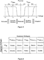
- Figure 3 shows an example of a diagram illustrating movable reflective layer position versus applied voltage for the IMOD of Figure 1 .
- the row/column (i.e., common/segment) write procedure may take advantage of a hysteresis property of these devices as illustrated in Figure 3 .
- An IMOD may require, for example, about a 10-volt potential difference to cause the movable reflective layer, or mirror, to change from the relaxed state to the actuated state.
- the movable reflective layer maintains its state as the voltage drops back below, e.g., 10 volts. However, the movable reflective layer does not relax completely until the voltage drops below 2 volts.
- a range of voltage approximately 3 to 7 volts, as shown in Figure 3 , exists where there is a window of applied voltage within which the device is stable in either the relaxed or actuated state. This is referred to herein as the "hysteresis window” or “stability window.”
- the row/column write procedure can be designed to address one or more rows at a time, such that during the addressing of a given row, pixels in the addressed row that are to be actuated are exposed to a voltage difference of about 10 volts, and pixels that are to be relaxed are exposed to a voltage difference of near zero volts.
- each pixel After addressing, the pixels are exposed to a steady state or bias voltage difference of approximately 5-volts such that they remain in the previous strobing state. In this example, after being addressed, each pixel sees a potential difference within the "stability window" of about 3-7 volts.
- This hysteresis property feature enables the pixel design, e.g., illustrated in Figure 1 , to remain stable in either an actuated or relaxed pre-existing state under the same applied voltage conditions. Since each IMOD pixel, whether in the actuated or relaxed state, is essentially a capacitor formed by the fixed and moving reflective layers, this stable state can be held at a steady voltage within the hysteresis window without substantially consuming or losing power. Moreover, essentially little or no current flows into the IMOD pixel if the applied voltage potential remains substantially fixed.
- a frame of an image may be created by applying data signals in the form of "segment" voltages along the set of column electrodes, in accordance with the desired change (if any) to the state of the pixels in a given row.
- Each row of the array can be addressed in turn, such that the frame is written one row at a time.
- segment voltages corresponding to the desired state of the pixels in the first row can be applied on the column electrodes, and a first row pulse in the form of a specific "common" voltage or signal can be applied to the first row electrode.
- the set of segment voltages can then be changed to correspond to the desired change (if any) to the state of the pixels in the second row, and a second common voltage can be applied to the second row electrode.
- the pixels in the first row are unaffected by the change in the segment voltages applied along the column electrodes, and remain in the state they were set to during the first common voltage row pulse.
- This process may be repeated for the entire series of rows, or alternatively, columns, in a sequential fashion to produce the image frame.
- the frames can be refreshed and/or updated with new image data by continually repeating this process at some desired number of frames per second.
- FIG. 4 shows an example of a table illustrating various states of an IMOD when various common and segment voltages are applied.
- the "segment” voltages can be applied to either the column electrodes or the row electrodes, and the “common” voltages can be applied to the other of the column electrodes or the row electrodes.
- the potential voltage across the modulator (alternatively referred to as a pixel voltage) is within the relaxation window (see Figure 3 , also referred to as a release window) both when the high segment voltage VS H and the low segment voltage VS L are applied along the corresponding segment line for that pixel.
- a hold voltage When a hold voltage is applied on a common line, such as a high hold voltage VC HOLD_H or a low hold voltage VC HOLD_L , the state of the IMOD will remain constant. For example, a relaxed IMOD will remain in a relaxed position, and an actuated IMOD will remain in an actuated position.
- the hold voltages can be selected such that the pixel voltage will remain within a stability window both when the high segment voltage VS H and the low segment voltage VS L are applied along the corresponding segment line.
- the segment voltage swing i.e., the difference between the high VS H and low segment voltage VS L , is less than the width of either the positive or the negative stability window.
- a common line such as a high addressing voltage VC ADD_H or a low addressing voltage VC ADD_L
- data can be selectively written to the modulators along that line by application of segment voltages along the respective segment lines.
- the segment voltages may be selected such that actuation is dependent upon the segment voltage applied.
- an addressing voltage is applied along a common line
- application of one segment voltage will result in a pixel voltage within a stability window, causing the pixel to remain unactuated.
- application of the other segment voltage will result in a pixel voltage beyond the stability window, resulting in actuation of the pixel.
- the particular segment voltage which causes actuation can vary depending upon which addressing voltage is used.
- the effect of the segment voltages can be the opposite when a low addressing voltage VC ADD_L is applied, with high segment voltage VS H causing actuation of the modulator, and low segment voltage VS L having no effect (i.e., remaining stable) on the state of the modulator.
- hold voltages, address voltages, and segment voltages may be used which always produce the same polarity potential difference across the modulators.
- signals can be used which alternate the polarity of the potential difference of the modulators. Alternation of the polarity across the modulators (that is, alternation of the polarity of write procedures) may reduce or inhibit charge accumulation which could occur after repeated write operations of a single polarity.
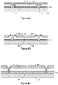
- Figure 5A shows an example of a diagram illustrating a frame of display data in the 3x3 IMOD display of Figure 2 .
- Figure 5B shows an example of a timing diagram for common and segment signals that may be used to write the frame of display data illustrated in Figure 5A .
- the signals can be applied to the, e.g., 3x3 array of Figure 2 , which will ultimately result in the line time 60e display arrangement illustrated in Figure 5A .
- the actuated modulators in Figure 5A are in a dark-state, i.e., where a substantial portion of the reflected light is outside of the visible spectrum so as to result in a dark appearance to, e.g., a viewer.
- the pixels Prior to writing the frame illustrated in Figure 5A , the pixels can be in any state, but the write procedure illustrated in the timing diagram of Figure 5B presumes that each modulator has been released and resides in an unactuated state before the first line time 60a.
- a release voltage 70 is applied on common line 1; the voltage applied on common line 2 begins at a high hold voltage 72 and moves to a release voltage 70; and a low hold voltage 76 is applied along common line 3.
- the modulators (common 1, segment 1), (1,2) and (1,3) along common line 1 remain in a relaxed, or unactuated, state for the duration of the first line time 60a, the modulators (2,1), (2,2) and (2,3) along common line 2 will move to a relaxed state, and the modulators (3,1), (3,2) and (3,3) along common line 3 will remain in their previous state.
- segment voltages applied along segment lines 1, 2 and 3 will have no effect on the state of the IMODs, as none of common lines 1, 2 or 3 are being exposed to voltage levels causing actuation during line time 60a (i.e., VC REL - relax and VC HOLD_L - stable).
- the voltage on common line 1 moves to a high hold voltage 72, and all modulators along common line 1 remain in a relaxed state regardless of the segment voltage applied because no addressing, or actuation, voltage was applied on the common line 1.
- the modulators along common line 2 remain in a relaxed state due to the application of the release voltage 70, and the modulators (3,1), (3,2) and (3,3) along common line 3 will relax when the voltage along common line 3 moves to a release voltage 70.
- common line 1 is addressed by applying a high address voltage 74 on common line 1. Because a low segment voltage 64 is applied along segment lines 1 and 2 during the application of this address voltage, the pixel voltage across modulators (1,1) and (1,2) is greater than the high end of the positive stability window (i.e., the voltage differential exceeded a predefined threshold) of the modulators, and the modulators (1,1) and (1,2) are actuated. Conversely, because a high segment voltage 62 is applied along segment line 3, the pixel voltage across modulator (1,3) is less than that of modulators (1,1) and (1,2), and remains within the positive stability window of the modulator; modulator (1,3) thus remains relaxed. Also during line time 60c, the voltage along common line 2 decreases to a low hold voltage 76, and the voltage along common line 3 remains at a release voltage 70, leaving the modulators along common lines 2 and 3 in a relaxed position.
- the voltage on common line 1 returns to a high hold voltage 72, leaving the modulators along common line 1 in their respective addressed states.
- the voltage on common line 2 is decreased to a low address voltage 78. Because a high segment voltage 62 is applied along segment line 2, the pixel voltage across modulator (2,2) is below the lower end of the negative stability window of the modulator, causing the modulator (2,2) to actuate. Conversely, because a low segment voltage 64 is applied along segment lines 1 and 3, the modulators (2,1) and (2,3) remain in a relaxed position.
- the voltage on common line 3 increases to a high hold voltage 72, leaving the modulators along common line 3 in a relaxed state.
- the voltage on common line 1 remains at high hold voltage 72, and the voltage on common line 2 remains at a low hold voltage 76, leaving the modulators along common lines 1 and 2 in their respective addressed states.
- the voltage on common line 3 increases to a high address voltage 74 to address the modulators along common line 3.
- the modulators (3,2) and (3,3) actuate, while the high segment voltage 62 applied along segment line 1 causes modulator (3,1) to remain in a relaxed position.
- the 3x3 pixel array is in the state shown in Figure 5A , and will remain in that state as long as the hold voltages are applied along the common lines, regardless of variations in the segment voltage which may occur when modulators along other common lines (not shown) are being addressed.
- a given write procedure (i.e., line times 60a-60e) can include the use of either high hold and address voltages, or low hold and address voltages.
- the pixel voltage remains within a given stability window, and does not pass through the relaxation window until a release voltage is applied on that common line.
- the actuation time of a modulator may determine the necessary line time.
- the release voltage may be applied for longer than a single line time, as depicted in Figure 5B .
- voltages applied along common lines or segment lines may vary to account for variations in the actuation and release voltages of different modulators, such as modulators of different colors.
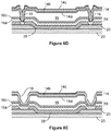
- Figures 6A-6E show examples of cross-sections of varying implementations of IMODs, including the movable reflective layer 14 and its supporting structures.
- Figure 6A shows an example of a partial cross-section of the IMOD display of Figure 1 , where a strip of metal material, i.e., the movable reflective layer 14 is deposited on supports 18 extending orthogonally from the substrate 20.
- the movable reflective layer 14 of each IMOD is generally square or rectangular in shape and attached to supports at or near the corners, on tethers 32.
- the movable reflective layer 14 is generally square or rectangular in shape and suspended from a deformable layer 34, which may include a flexible metal.
- the deformable layer 34 can connect, directly or indirectly, to the substrate 20 around the perimeter of the movable reflective layer 14. These connections are herein referred to as support posts.
- the implementation shown in Figure 6C has additional benefits deriving from the decoupling of the optical functions of the movable reflective layer 14 from its mechanical functions, which are carried out by the deformable layer 34. This decoupling allows the structural design and materials used for the reflective layer 14 and those used for the deformable layer 34 to be optimized independently of one another.
- Figure 6D shows another example of an IMOD, where the movable reflective layer 14 includes a reflective sub-layer 14a.
- the movable reflective layer 14 rests on a support structure, such as support posts 18.
- the support posts 18 provide separation of the movable reflective layer 14 from the lower stationary electrode (i.e., part of the optical stack 16 in the illustrated IMOD) so that a gap 19 is formed between the movable reflective layer 14 and the optical stack 16, for example when the movable reflective layer 14 is in a relaxed position.
- the movable reflective layer 14 also can include a conductive layer 14c, which may be configured to serve as an electrode, and a support layer 14b.
- the conductive layer 14c is disposed on one side of the support layer 14b, distal from the substrate 20, and the reflective sub-layer 14a is disposed on the other side of the support layer 14b, proximal to the substrate 20.
- the reflective sub-layer 14a can be conductive and can be disposed between the support layer 14b and the optical stack 16.
- the support layer 14b can include one or more layers of a dielectric material, for example, silicon oxynitride (SiON) or silicon dioxide (SiO 2 ).
- the support layer 14b can be a stack of layers, such as, for example, an SiO 2 /SiON/SiO 2 tri-layer stack.
- Either or both of the reflective sub-layer 14a and the conductive layer 14c can include, e.g., an aluminum (Al) alloy with about 0.5% copper (Cu), or another reflective metallic material.
- Al aluminum
- Cu copper
- Employing conductive layers 14a, 14c above and below the dielectric support layer 14b can balance stresses and provide enhanced conduction.
- the reflective sub-layer 14a and the conductive layer 14c can be formed of different materials for a variety of design purposes, such as achieving specific stress profiles within the movable reflective layer 14.
- some implementations also can include a black mask structure 23.
- the black mask structure 23 can be formed in optically inactive regions (e.g., between pixels or under posts 18) to absorb ambient or stray light.
- the black mask structure 23 also can improve the optical properties of a display device by inhibiting light from being reflected from or transmitted through inactive portions of the display, thereby increasing the contrast ratio.
- the black mask structure 23 can be conductive and be configured to function as an electrical bussing layer.
- the row electrodes can be connected to the black mask structure 23 to reduce the resistance of the connected row electrode.
- the black mask structure 23 can be formed using a variety of methods, including deposition and patterning techniques.
- the black mask structure 23 can include one or more layers.
- the black mask structure 23 includes a molybdenum-chromium (MoCr) layer that serves as an optical absorber, an SiO 2 layer, and an aluminum alloy that serves as a reflector and a bussing layer, with a thickness in the range of about 30-80 ⁇ , 500-1000 ⁇ , and 500-6000 ⁇ , respectively.
- the one or more layers can be patterned using a variety of techniques, including photolithography and dry etching, including, for example, carbon tetrafluoromethane (CF 4 ) and/or oxygen (O 2 ) for the MoCr and SiO 2 layers and chlorine (Cl 2 ) and/or boron trichloride (BCl 3 ) for the aluminum alloy layer.
- the black mask 23 can be an etalon or interferometric stack structure.
- the conductive absorbers can be used to transmit or bus signals between lower, stationary electrodes in the optical stack 16 of each row or column.
- a spacer layer 35 can serve to generally electrically isolate the absorber layer 16a from the conductive layers in the black mask 23.
- Figure 6E shows another example of an IMOD, where the movable reflective layer 14 is self-supporting.
- the implementation of Figure 6E does not include support posts 18. Instead, the movable reflective layer 14 contacts the underlying optical stack 16 at multiple locations, and the curvature of the movable reflective layer 14 provides sufficient support that the movable reflective layer 14 returns to the unactuated position of Figure 6E when the voltage across the IMOD is insufficient to cause actuation.
- the IMODs function as direct-view devices, in which images are viewed from the front side of the transparent substrate 20, i.e., the side opposite to that upon which the modulator is arranged.
- the back portions of the device that is, any portion of the display device behind the movable reflective layer 14, including, for example, the deformable layer 34 illustrated in Figure 6C
- the reflective layer 14 optically shields those portions of the device.
- a bus structure (not illustrated) can be included behind the movable reflective layer 14 which provides the ability to separate the optical properties of the modulator from the electromechanical properties of the modulator, such as voltage addressing and the movements that result from such addressing.
- the implementations of Figures 6A-6E can simplify processing, such as patterning.
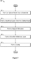
- Figure 7 shows an example of a flow diagram illustrating a manufacturing process 80 for an IMOD
- Figures 8A-8E show examples of cross-sectional schematic illustrations of corresponding stages of such a manufacturing process 80.
- the manufacturing process 80 can be implemented to manufacture, e.g., IMODs of the general type illustrated in Figures 1 and 6 , in addition to other blocks not shown in Figure 7 .
- the process 80 begins at block 82 with the formation of the optical stack 16 over the substrate 20.
- Figure 8A illustrates such an optical stack 16 formed over the substrate 20.
- the substrate 20 may be a transparent substrate such as glass or plastic, it may be flexible or relatively stiff and unbending, and may have been subjected to prior preparation processes, e.g., cleaning, to facilitate efficient formation of the optical stack 16.
- the optical stack 16 can be electrically conductive, partially transparent and partially reflective and may be fabricated, for example, by depositing one or more layers having the desired properties onto the transparent substrate 20.
- the optical stack 16 includes a multilayer structure having sub-layers 16a and 16b, although more or fewer sub-layers may be included in some other implementations.
- one of the sub-layers 16a, 16b can be configured with both optically absorptive and conductive properties, such as the combined conductor/absorber sub-layer 16a. Additionally, one or more of the sub-layers 16a, 16b can be patterned into parallel strips, and may form row electrodes in a display device. Such patterning can be performed by a masking and etching process or another suitable process known in the art. In some implementations, one of the sub-layers 16a, 16b can be an insulating or dielectric layer, such as sub-layer 16b that is deposited over one or more metal layers (e.g., one or more reflective and/or conductive layers). In addition, the optical stack 16 can be patterned into individual and parallel strips that form the rows of the display.
- the process 80 continues at block 84 with the formation of a sacrificial layer 25 over the optical stack 16.
- the sacrificial layer 25 is later removed (e.g., at block 90) to form the cavity 19 and thus the sacrificial layer 25 is not shown in the resulting IMODs 12 illustrated in Figure 1 .
- Figure 8B illustrates a partially fabricated device including a sacrificial layer 25 formed over the optical stack 16.
- the formation of the sacrificial layer 25 over the optical stack 16 may include deposition of a xenon difluoride (XeF 2 )-etchable material such as molybdenum (Mo) or amorphous silicon (Si), in a thickness selected to provide, after subsequent removal, a gap or cavity 19 (see also Figures 1 and 8E ) having a desired design size.
- XeF 2 xenon difluoride
- Mo molybdenum
- Si amorphous silicon
- Deposition of the sacrificial material may be carried out using deposition techniques such as physical vapor deposition (PVD, e.g., sputtering), plasma-enhanced chemical vapor deposition (PECVD), thermal chemical vapor deposition (thermal CVD), or spin-coating.
- PVD physical vapor deposition
- PECVD plasma-enhanced chemical vapor deposition
- thermal CVD thermal chemical vapor deposition
- the process 80 continues at block 86 with the formation of a support structure e.g., a post 18 as illustrated in Figures 1 , 6 and 8C .
- the formation of the post 18 may include patterning the sacrificial layer 25 to form a support structure aperture, then depositing a material (e.g., a polymer or an inorganic material, e.g., silicon oxide) into the aperture to form the post 18, using a deposition method such as PVD, PECVD, thermal CVD, or spin-coating.
- a material e.g., a polymer or an inorganic material, e.g., silicon oxide
- the support structure aperture formed in the sacrificial layer can extend through both the sacrificial layer 25 and the optical stack 16 to the underlying substrate 20, so that the lower end of the post 18 contacts the substrate 20 as illustrated in Figure 6A .
- the aperture formed in the sacrificial layer 25 can extend through the sacrificial layer 25, but not through the optical stack 16.
- Figure 8E illustrates the lower ends of the support posts 18 in contact with an upper surface of the optical stack 16.
- the post 18, or other support structures may be formed by depositing a layer of support structure material over the sacrificial layer 25 and patterning portions of the support structure material located away from apertures in the sacrificial layer 25.
- the support structures may be located within the apertures, as illustrated in Figure 8C , but also can, at least partially, extend over a portion of the sacrificial layer 25.
- the patterning of the sacrificial layer 25 and/or the support posts 18 can be performed by a patterning and etching process, but also may be performed by alternative etching methods.
- the process 80 continues at block 88 with the formation of a movable reflective layer or membrane such as the movable reflective layer 14 illustrated in Figures 1 , 6 and 8D .
- the movable reflective layer 14 may be formed by employing one or more deposition processes, e.g., reflective layer (e.g., aluminum, aluminum alloy) deposition, along with one or more patterning, masking, and/or etching processes.
- the movable reflective layer 14 can be electrically conductive, and referred to as an electrically conductive layer.
- the movable reflective layer 14 may include a plurality of sub-layers 14a, 14b, 14c as shown in Figure 8D .
- one or more of the sub-layers may include highly reflective sub-layers selected for their optical properties, and another sub-layer 14b may include a mechanical sub-layer selected for its mechanical properties. Since the sacrificial layer 25 is still present in the partially fabricated IMOD formed at block 88, the movable reflective layer 14 is typically not movable at this stage. A partially fabricated IMOD that contains a sacrificial layer 25 also may be referred to herein as an "unreleased" IMOD. As described above in connection with Figure 1 , the movable reflective layer 14 can be patterned into individual and parallel strips that form the columns of the display.
- the process 80 continues at block 90 with the formation of a cavity, e.g., cavity 19 as illustrated in Figures 1 , 6 and 8E .
- the cavity 19 may be formed by exposing the sacrificial material 25 (deposited at block 84) to an etchant.
- an etchable sacrificial material such as Mo or amorphous Si may be removed by dry chemical etching, e.g., by exposing the sacrificial layer 25 to a gaseous or vaporous etchant, such as vapors derived from solid XeF 2 for a period of time that is effective to remove the desired amount of material, typically selectively removed relative to the structures surrounding the cavity 19.
- etchable sacrificial material and etching methods e.g. wet etching and/or plasma etching
- etching methods e.g. wet etching and/or plasma etching
- the movable reflective layer 14 is typically movable after this stage.
- the resulting fully or partially fabricated IMOD may be referred to herein as a "released" IMOD.
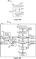
- Figure 9 shows an example of a flow diagram illustrating blocks of a method of invoking device operations when the presence of an ear is detected.
- the method 900 may be performed, at least in part, by a logic system of a mobile device, such as the display devices 40 shown in Figures 10A-10K, 16A or 16B .
- the logic system may include a general purpose single- or multi-chip processor, a digital signal processor (DSP), an application specific integrated circuit (ASIC), a field programmable gate array (FPGA) or other programmable logic device, discrete gate or transistor logic, discrete hardware components, or any combination thereof.
- DSP digital signal processor
- ASIC application specific integrated circuit
- FPGA field programmable gate array
- the blocks of method 900 are not necessarily performed in the order shown.
- Alternative implementations of the method 900 may include more or fewer blocks.
- block 905 involves scanning a touch sensor array, such as a projected capacitive touch sensor array.
- block 910 involves detecting array capacitances of a touch sensor array.
- blocks 905 and/or 910 also may involve receiving sensor signals from other types of sensors, such as a pressure sensor, an infrared (IR) sensor, an accelerometer, a gyroscope, an orientation sensor, and/or a camera.
- the sensor signals from the other types of sensors may be received to augment the signals from the touch sensor array.
- the sensor signals may then be analyzed.
- array capacitances of the touch sensor array are analyzed. It may then be determined whether the array capacitances indicate the presence of an ear, such as an ear of a user of a mobile device.
- Blocks 915 and/or 920 may involve a number of sub-processes, such as determining a pattern of array capacitance values and comparing the pattern to ear pattern data and/or face pattern data stored in a memory.
- the ear pattern data and/or face pattern data may have been previously acquired and stored during a "setup" or registration process.
- a device operation may involve controlling at least one speaker of a cell phone.
- a device operation may involve switching to a speaker phone mode, switching to a normal audio mode, adjusting a volume of an audio output device, adjusting a directionality of an audio output device, adjusting a directionality of a microphone, etc. For example, when the presence of an ear is detected, the volume of a cell phone speaker may be reduced. In a second example, when the presence of an ear or of a particular ear is detected, the cell phone may be unlocked or powered up. In a third example, a voice recognition capability may be invoked or negated when the presence of an ear is detected. Other examples are described below.
- a logic system of a mobile device may receive user input indicating that the method 900 will terminate.
- the logic system may receive input that the mobile device will be switched off, that the mobile device will be operated in a gaming mode, etc. If so, the method 900 may end, as shown in block 935.
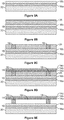
- FIGS 10A-10D show examples of various ear detection states of a projected capacitive touch sensor array and corresponding speaker settings.
- the display device 40 includes a cell phone with a touch sensor array 1000 positioned over the display array 30.
- the touch sensor array 1000 is a projected capacitive touch sensor array.
- alternative implementations may include another type of touch sensor array, such as a digital resistive touch (DRT) sensor array.
- DDT digital resistive touch
- the row 1010 includes a rectangle for each of Figures 10A-10D . Each rectangle indicates a corresponding audio volume for the speaker 45.
- the row 1015 indicates whether the cell phone will be used in "speaker phone" mode: the large rectangle in the row 1015 of Figure 10A indicates that the cell phone is configured for speaker phone mode, whereas the small rectangles in the row 1015 of Figures 10B-10D indicate that the cell phone is not configured for speaker phone mode.
- the sensitivity of the microphone 46 may be increased when the cell phone is configured for speaker phone mode.
- the touch sensor array 1000 includes a plurality of sensor elements or "sensels" 1005.
- each sensel 1005 is shown with a number between zero and nine. This number represents the detected capacitance change for each sensel 1005 from a baseline level. Such changes may be caused by the presence of a conductive material, such as a finger, a conductive stylus, an ear, the side of a face, etc. These numbers are shown merely by way of illustration; an actual touch sensor would generally not display such numbers, nor do the changes need be represented by a number between 0 and 9 inclusively.
- the values of the capacitance or capacitance changes may be represented by a signed or unsigned binary number with four to fourteen bits of data.
- all of the sensels 1005 indicate a value of zero, which is the baseline value in this example.
- Figure 10A represents an instance during which the array capacitances indicate the presence of no external material in the vicinity of the touch sensor array 1000.
- the logic system may determine that the array capacitances do not indicate the presence of an ear.
- the cell phone of the display device 40 when the cell phone of the display device 40 is in use, the cell phone may be configured for speaker phone mode when no ear is detected.
- FIG 10B many of the sensels 1005 indicate non-zero array capacitance values.
- Figure 10B represents an instance during which the array capacitances indicate an ear lightly touching the touch sensor array 1000.
- an ear touch zone 1020a will be determined, e.g., according to a contouring or pattern recognition program.
- ear touch zone 1020a roughly corresponds to a surface contact area between an ear and the display array 30.
- a device operation is invoked: the cell phone will not be configured for speaker phone mode because an ear is detected.
- the audio volume is set at a relatively low level.
- a light ear touch corresponds to a fewer number of sensels 1005 detecting contact, or a value change from baseline that is relatively lower than a value corresponding to a heavier ear touch.
- the audio volume level will be based, at least in part, on the area of the ear touch zone 1020a.
- Figure 10C many of the sensels 1005 indicate higher array capacitance values than those of Figure 10B . Therefore, the area of the ear touch zone 1020b is determined to be relatively larger than that of the ear touch zone 1020a.
- Figure 10C represents an instance during which an ear is being pressed against the touch sensor array 1000 with a moderate force. Accordingly, in block 925 of Figure 9 , a slightly different device operation is invoked: because a moderate ear touch has been detected, the audio volume is set at a relatively higher level than in the example shown in Figure 10B .
- the audio volume level will be increased, based on an assumption that a user is pressing his or her ear against the cell phone with increased force in an attempt to hear more clearly the sounds from the speaker 45.
- the audio volume may be adjusted differently in alternative implementations.
- Figure 10D many of the sensels 1005 indicate yet higher array capacitance values than those of Figure 10C . Therefore, the area of the ear touch zone 1020c is determined to be even larger than that of the ear touch zone 1020b.
- Figure 10D represents an instance during which an ear is being pressed against the touch sensor array 1000 with a substantial, heavy force. In this example, part of the user's face is also being pressed against the touch sensor array 1000, such that a face touch zone 1025 is detected in block 920 of Figure 9 .
- the device operation may involve tracking an ear position and/or orientation.
- Microphone, speaker and/or other device functionality may be adjusted according to the ear position and/or orientation. For example, referring to Figure 10B , when it is determined that the ear touch zone 1020a moves downward, such as in the direction of the arrow 1030, the user's ear will be farther from the speaker 45. In some implementations, the audio volume may be increased in order to compensate for this change in ear position relative to the speaker 45.
- Microphone sensitivity also may be adjusted according to a determined change in a user's mouth position, which may be inferred from an ear rotation or translation.
- the device operations invoked in block 925 may involve voice commands and/or voice recognition functionality.
- a device may control voice recognition functionality according to whether an ear and/or an ear gesture is detected. For example, a voice recognition feature may be turned on or turned off when an ear is detected.
- the device operation of block 925 may involve recognizing a characteristic pattern of an ear and/or a portion of a face.
- block 925 may involve detecting a left ear, detecting a right ear, and/or recognizing a particular ear.
- ear recognition may be used as a type of user authentication.
- an ear recognition process may be used in lieu of (or in addition to) an authorization code, such as a personal identification number (PIN).
- the ear recognition process may invoke device operations for accessing a mobile device, unlocking a mobile device, etc.
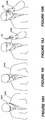
- Figures 10E-10G show an example of unlocking or turning on a mobile device for a phone conversation when the presence of an ear is detected.
- the mobile display device 40 with speaker 45 and microphone 46 has a display array 30 including an overlaid or integral touch sensor array 1000.
- the sensor elements or sensels 1005 of the touch sensor array 1000 illustratively show in Figure 10E small or essentially zero capacitance changes at each sensel.
- the display device 40 may be positioned near an ear of the user as indicated by ear touch zone 1020 in Figure 10F to unlock, power up, or otherwise initiate one or more functions of the device, and allow the user to commence with speaking or listening to a phone conversation, as indicated in Figure 10G .
- the user may listen, for example, to sound emanating from speaker 45 or speak into microphone 46.
- the user's ear may continue to be pressed against the ear touch zone 1020' of the mobile device, or pulled away from the mobile device for speaker phone operation or for interaction with the touch sensor array 1000 using one or more fingers.
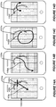
- Figures 10H-10K show an example of a user of a mobile device with and without an ear-detection capability.
- a user 1040 with an ear 1045 may fumble with a mobile device as shown in Figures 10H and 10I , before bringing the mobile display device 40 towards the user's head, as shown in Figure 10J .
- a user 1040 with a mobile display device 40 having ear position or gesture detection capability may immediately bring the mobile device to the ear without fumbling with the device, as shown in Figure 10K , thereby avoiding the need to either look at the mobile device or touch particular locations on a touchscreen of the mobile device before device operation is allowed.
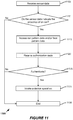
- FIG. 11 shows an example of a flow diagram illustrating blocks of an ear authentication method.
- Method 1100 may be performed, at least in part, by a logic system of a display device 40.
- method 1100 begins with block 1105, in which sensor data are received by the logic system.
- the sensor data may include signals from a touch sensor, such as the touch sensor array 1000.
- the sensor data also may include data from a camera, an infrared (IR) sensor, a pressure sensor, an accelerometer, a gyroscope, an orientation sensor, and/or another type of sensor.
- IR infrared
- the logic system determines whether the sensor data indicated the presence of an ear. If so, ear pattern and/or face pattern data are accessed by the logic system in block 1115. Such data may be stored in a storage medium of the display device or of another device, e.g., by a storage device accessible by the logic system via a network.
- Implementations that enable ear and/or face recognition to be used as a type of user authentication can provide varying levels of device security.
- an ear recognition/authentication process alone may be sufficient to invoke device operations, such as allowing device access or unlocking or powering up a mobile device.
- Using an ear recognition process in addition to an authorization code can provide a relatively higher level of security.
- requiring the use of an authorization code may be less convenient for users.
- method 1100 includes an optional process of receiving an additional authorization code, such as a PIN, an alphanumeric password or passcode, a voice recognition input, etc. as shown in optional block 1120.
- the logic system determines whether the stored ear pattern data match the sensor data received in block 1105.
- the logic system also may determine whether the authorization code is correct.
- block 1130 may involve allowing access to other functions of a mobile device.
- a user may, for example, be able to initiate a cell phone call, unlock a device, use a web browser, access an account, etc.
- method 1100 ends (block 1135) after the device operation is invoked.
- Method 1100 also ends if the authentication process of block 1125 fails, e.g., for a predetermined number of times or the sensor data do not indicate the presence of an ear in block 1110.
- method 1100 may continue if, for example, the sensor data do not initially indicate the presence of an ear in block 1110.
- Sensor data may continue to be received in block 1105 and evaluated in block 1110 for a predetermined time and/or until the occurrence of one or more predetermined conditions.
- the ear authentication method described above involves the use of previously-acquired ear pattern and/or face pattern data. Some implementations described herein provide methods for acquiring and storing such data.
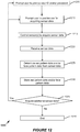
- Figure 12 shows an example of a flow diagram illustrating blocks of a method for acquiring and storing ear pattern data and/or face pattern data.
- Method 1200 may be performed, at least in part, by a logic system of a display device 40. In some implementations, the blocks of method 1200 may be sub-processes of block 925 (see Figure 9 ).
- method 1200 begins with optional block 1205, in which a user is prompted to enter a user identification code and/or a password. Such information may, for example, be used to associate a particular user with a set of ear pattern and/or face pattern data.
- a user is prompted to position an ear for acquiring sensor data. The prompts may, for example, indicate where the user's ear should be positioned.
- block 1210 may involve a visual prompt that is displayed on a display device.
- block 1210 may involve audio prompts.
- Audio prompts may be advantageous if ear pattern data are to be acquired from a sensor or a sensor array that is located near a display.
- audio prompts may be advantageous if ear pattern data are to be acquired from a touch sensor array, because a user will not generally be able to see the touch sensor array when the user's ear is pressed against the display device. Even if the sensor data will be acquired by another type of sensor, audio prompts may still be advantageous. Due to the small size of many display devices 40, it may be difficult for a user to see prompts displayed on the display array 30 while sensor data are being acquired from the user's ear.
- the prompts may indicate how hard the user should press an ear against the touch sensor array.
- the display device 40 may include one or more pressure or force sensors. When a user is pressing the ear against the touch sensor array, the pressure sensor(s) may indicate corresponding pressure data.
- a logic system of the display device 40 may be configured to receive the pressure data from the pressure sensor(s), to determine whether the ear is being pressed hard enough against the touch sensor array, too hard, etc.
- the logic system may be configured to control the speaker 45 to provide corresponding voice prompts to the user.
- the logic system may control the sensor(s) to acquire the sensor data (block 1215).
- the raw sensor data may be stored.
- a logic system will receive the sensor data (block 1220) and determine ear pattern data and/or face pattern data from the sensor data (block 1225).
- the logic system may determine the ear pattern data and/or face pattern data according to an algorithm, such as a contouring or pattern recognition algorithm.
- sensor array data such as array capacitances, may be input into the algorithm.
- the ear touch zones 1020a-1020c shown in Figures 10B-10D provide examples of contoured ear patterns that may be output from such algorithms.
- the ear pattern data and/or face pattern data may be stored in block 1230.
- block 1235 it is determined whether additional sensor data will be acquired. This determination may be made by the logic system and/or according to user input. In some implementations, more than one type of sensor data will be acquired for a user. In other implementations, multiple instances of the same type of sensor data will be acquired for a user. For example, a user may be prompted so that sensor data may be acquired with the user's ear in more than one position. The user may be prompted so that data may be acquired for a left ear and a right ear. The user may be prompted so that data may be acquired at varying pressures, such as the varying pressures indicated in Figures 10B-10D . If sensor data will be acquired for another user, in some implementations the process will revert to block 1205. The process ends with block 1240.
- FIG. 13 shows an example of a flow diagram illustrating blocks of a method of invoking device operations when an ear gesture is detected.
- Method 1300 may be performed, at least in part, by a logic system of a mobile device.
- the method 1300 begins with a process of scanning a sensor array (block 1305) and detecting sensor signals from the array (block 1310).
- block 1305 involves scanning a touch sensor array, such as a projected capacitive touch sensor array.
- blocks 1305 and/or 1310 also may involve receiving sensor signals from other types of sensors, such as a pressure sensor, an IR sensor, an accelerometer, a gyroscope, an orientation sensor, and/or a camera.
- the sensor signals may then be analyzed (block 1315).
- array capacitances of the touch sensor array are analyzed. It may then be determined whether the array capacitances indicate not only the presence of an ear, but of an ear gesture (block 1320).
- the ear gesture may be, for example, an ear touch, an ear press, an ear swipe, an ear rotation, an ear position, an ear distance, and/or an ear motion.
- an ear gesture may be caused primarily by force and/or motion of a hand holding a mobile device against the ear while the ear remains relatively stationary. Alternatively, or additionally, the ear gesture may actually be caused, at least in part, by force and/or motion of the ear while the mobile device remains relatively stationary.
- Figures 14A-14D show examples of ear gestures.
- each of the ear gestures, as well as other ear gestures not shown in these examples, may be associated with a device operation.
- the ear touch zone 1020a corresponds to the "light force" condition of Figure 10B , as detected by a touch sensor.
- ear gestures may be detected by a variety of sensors. If the ear gestures are detected by a touch sensor, ear gestures also may be made when the ear is pressed against the touch sensor with a moderate force or a heavy force, for example as shown in Figures 10C and 10D .
- Figure 14A shows examples of linear ear swipes.
- the ear gesture 1405a is a substantially linear swipe along columns of the touch sensor array 1000
- the ear gesture 1405b is a substantially linear swipe along rows of the touch sensor array 1000
- the ear gesture 1405c is a substantially diagonal swipe along rows and columns of the touch sensor array 1000.
- Each of these ear gestures may be associated with device operations.
- the direction of the swipe may or may not matter, depending on the implementation.
- the same device operation(s) may be associated with the ear gesture 1405a, regardless of whether an upward or a downward ear swipe is detected.
- a downward swipe may be associated with a first device operation and an upward swipe may be associated with a second device operation.
- the logic system may determine that the corresponding sensor signals indicate a type of ear gesture in block 1320 (see Figure 13 ).
- a corresponding device operation may be invoked in block 1325.
- the trajectories of the ear gestures 1405a-1405c are merely made by way of example; for example, diagonal ear swipes having other trajectories could be registered as ear gestures and associated with device operations.
- ear gestures do not necessarily involve swipes along substantially straight lines.
- the ear gesture 1405d is a swipe along a curved line.
- Other ear gestures may involve swipes along simpler or more complex trajectories or patterns.
- the ear gesture 1405e is a swipe in a generally oval pattern.
- Alternative ear gestures may involve swipes in other types of patterns, such as circular patterns, square patterns, rectangular patterns, triangular patterns, sequences of gestures separated by temporary withdrawal of the device from the ear, etc.
- an ear gesture may be associated with the shape of a pattern and not necessarily with the orientation of the pattern.
- a triangular ear gesture may be recognized by a detected triangular pattern, regardless of the orientation of each side of the triangle relative to rows or columns of a sensor array.
- ear gesture 1405f of Figure 14D provides an example of rotational ear gestures.
- a clockwise ear gesture may be associated with a first device operation and a counterclockwise ear gesture may be associated with a second device operation.
- a counterclockwise gesture may be associated with accepting an incoming call, and a clockwise gesture may be associated with hanging up the phone or ending the call.
- Figures 10B-10D also provide examples of ear gestures. These drawings show examples of "ear press" types of ear gestures.
- the logic system may determine that the corresponding sensor signals indicate a type of ear gesture in block 1320 (see Figure 13 ). Accordingly, a device operation may be invoked in block 1325. The device operation may involve switching to a speaker phone mode, switching to a normal audio mode, adjusting a volume of an audio output device, adjusting a directionality of an audio output device, adjusting a directionality of a microphone, etc.
- block 1330 of Figure 13 it is determined whether the method 1300 will continue. This determination may be made by the logic system and/or according to user input. In this example, if method 1300 will continue, the process reverts to block 1305. If not, the process ends, as in block 1335.
- Some implementations may involve machine learning processes for associating a detected ear or a detected ear gesture with a device operation. Some such learning processes may include receiving and storing user input regarding device functionality. Some implementations may include registration or calibration procedures.
- Figure 15 shows an example of a flow diagram illustrating blocks of an ear gesture registration method.
- Method 1500 may be performed, at least in part, by a logic system of a mobile device such as the display device 40.
- method 1500 begins when the logic system receives user input for initiating an ear gesture registration process, as in block 1505.
- Such input may, for example, be received as sensor signals corresponding to a user's interaction with the touch sensor array 1000, as a voice command received via the microphone 46, etc.
- block 1510 the user is prompted to select an ear gesture type and a device operation to associate with the ear gesture.
- the user may be prompted to indicate whether the ear gesture will be a substantially linear ear swipe, a curved ear swipe, a pattern (circular, oval, triangular, etc.), an ear press, a sequence of gestures, etc.
- block 1510 may involve receiving user input regarding a first desired speaker volume level to be applied when a cell phone is pressed against the user's ear with a first pressure and/or regarding a second desired speaker volume level to be applied when the cell phone is pressed against the user's ear with a second pressure.
- the user may not be prompted to indicate the type of ear gesture. Instead, the ear gesture trajectory and/or pattern type may be determined according to received sensor data.
- Some implementations also may involve associating the ear gesture type and the device operation(s) with a particular user. For example, the user may be prompted to enter user information, such as a user name, a user ID and/or a password or passcode.
- the user may be prompted to make the ear gesture.
- One or more sensors may be controlled to acquire sensor data (block 1520), which may be received by a logic device in block 1525.
- the logic device may analyze the sensor data to determine a corresponding ear gesture trajectory and/or pattern (block 1530). For example, block 1530 may involve determining whether the ear gesture trajectory and/or pattern type detected by the sensor(s) corresponds to the type indicated by the user in block 1510. If not, the logic system may determine that additional sensor data should be acquired (block 1535). Accordingly, the process may revert to block 1515.
- the logic system may acquire multiple instances of an ear gesture trajectory and/or pattern even if the first instance is satisfactory.
- the ear gesture trajectory and/or pattern data may be stored and associated with the indicated device operation(s), as shown in block 1540.
- block 1545 it is determined whether the process will continue. For example, the logic system may prompt the user for input regarding whether additional ear gesture trajectory and/or pattern data is or will be acquired. If so, the process may revert to block 1510. If not, the process may end, as in block 1550.
- FIGS 16A and 16B show examples of system block diagrams that illustrate a display device that may be configured to perform at least some methods described herein.
- the display device 40 can be, for example, a cellular or mobile telephone.
- the same components of the display device 40 or slight variations thereof are also illustrative of various types of display devices such as televisions, e-readers and portable media players.
- the display device 40 includes a housing 41, a display 30, a touch sensor array 1000, an antenna 43, a speaker 45, an input device 48, and a microphone 46.
- the housing 41 can be formed from any of a variety of manufacturing processes, including injection molding, and vacuum forming.
- the housing 41 may be made from any of a variety of materials, including, but not limited to: plastic, metal, glass, rubber, and ceramic, or a combination thereof.
- the housing 41 can include removable portions (not shown) that may be interchanged with other removable portions of different color, or containing different logos, pictures, or symbols.
- the display 30 may be any of a variety of displays, including a bi-stable or analog display, as described herein.
- the display 30 also can be configured to include a flat-panel display, such as plasma, EL, OLED, STN LCD, or TFT LCD, or a non-flat-panel display, such as a CRT or other tube device.
- the display 30 can include an IMOD display, as described herein.
- the components of the display device 40 are schematically illustrated in Figure 16B .
- the display device 40 includes a housing 41 and can include additional components at least partially enclosed therein.
- the display device 40 includes a network interface 27 that includes an antenna 43 which is coupled to a transceiver 47.
- the transceiver 47 is connected to a processor 21, which is connected to conditioning hardware 52.
- the conditioning hardware 52 may be configured to condition a signal (e.g., filter a signal).
- the conditioning hardware 52 is connected to a speaker 45 and a microphone 46.
- the processor 21 is also connected to an input device 48 and a driver controller 29.
- the driver controller 29 is coupled to a frame buffer 28, and to an array driver 22, which in turn is coupled to a display array 30.
- a power supply 50 can provide power to all components as required by the particular display device 40 design.
- the display device 40 also includes a sensor system 77.
- the sensor system 77 includes the touch sensor array 1000.
- the sensor system 77 also may include other types of sensors, such as one or more cameras, pressure sensors, infrared (IR) sensors, accelerometers, gyroscopes, orientation sensors, etc.
- the sensor system 77 may include part of the logic system of the display device 40.
- the sensor system 77 may include a touch controller that is configured to control, at least in part, the operations of the touch sensor array 1000.
- the processor 21 (or another such device) may be configured to provide some or all of this functionality.
- the network interface 27 includes the antenna 43 and the transceiver 47 so that the display device 40 can communicate with one or more devices over a network.
- the network interface 27 also may have some processing capabilities to relieve, e.g., data processing requirements of the processor 21.
- the antenna 43 can transmit and receive signals.
- the antenna 43 transmits and receives RF signals according to the IEEE 16.11 standard, including IEEE 16.11 (a), (b), or (g), or the IEEE 802.11 standard, including IEEE 802.11 a, b, g or n.
- the antenna 43 transmits and receives RF signals according to the BLUETOOTH standard.
- the antenna 43 is designed to receive code division multiple access (CDMA), frequency division multiple access (FDMA), time division multiple access (TDMA), Global System for Mobile communications (GSM), GSM/General Packet Radio Service (GPRS), Enhanced Data GSM Environment (EDGE), Terrestrial Trunked Radio (TETRA), Wideband-CDMA (W-CDMA), Evolution Data Optimized (EV-DO), 1xEV-DO, EV-DO Rev A, EV-DO Rev B, High Speed Packet Access (HSPA), High Speed Downlink Packet Access (HSDPA), High Speed Uplink Packet Access (HSUPA), Evolved High Speed Packet Access (HSPA+), Long Term Evolution (LTE), AMPS, or other known signals that are used to communicate within a wireless network, such as a system utilizing 3G or 4G technology.
- CDMA code division multiple access
- FDMA frequency division multiple access
- TDMA Time division multiple access
- GSM Global System for Mobile communications
- GPRS GSM/General Packet
- the transceiver 47 can pre-process the signals received from the antenna 43 so that they may be received by and further manipulated by the processor 21.
- the transceiver 47 also can process signals received from the processor 21 so that they may be transmitted from the display device 40 via the antenna 43.
- the processor 21 may be configured to receive time data, e.g., from a time server, via the network interface 27.
- the transceiver 47 can be replaced by a receiver.
- the network interface 27 can be replaced by an image source, which can store or generate image data to be sent to the processor 21.
- the processor 21 can control the overall operation of the display device 40.
- the processor 21 receives data, such as compressed image data from the network interface 27 or an image source, and processes the data into raw image data or into a format that is readily processed into raw image data.
- the processor 21 can send the processed data to the driver controller 29 or to the frame buffer 28 for storage.
- Raw data typically refers to the information that identifies the image characteristics at each location within an image. For example, such image characteristics can include color, saturation, and gray-scale level.
- the processor 21 can include a microcontroller, CPU, or logic unit to control operation of the display device 40.
- the conditioning hardware 52 may include amplifiers and filters for transmitting signals to the speaker 45, and for receiving signals from the microphone 46.
- the conditioning hardware 52 may be discrete components within the display device 40, or may be incorporated within the processor 21 or other components.
- the driver controller 29 can take the raw image data generated by the processor 21 either directly from the processor 21 or from the frame buffer 28 and can re-format the raw image data appropriately for high speed transmission to the array driver 22. In some implementations, the driver controller 29 can re-format the raw image data into a data flow having a raster-like format, such that it has a time order suitable for scanning across the display array 30. Then the driver controller 29 sends the formatted information to the array driver 22.
- a driver controller 29, such as an LCD controller is often associated with the system processor 21 as a stand-alone integrated circuit (IC), such controllers may be implemented in many ways. For example, controllers may be embedded in the processor 21 as hardware, embedded in the processor 21 as software, or fully integrated in hardware with the array driver 22.
- the array driver 22 can receive the formatted information from the driver controller 29 and can re-format the video data into a parallel set of waveforms that are applied many times per second to the hundreds, and sometimes thousands (or more), of leads coming from the display's x-y matrix of pixels.
- the driver controller 29, the array driver 22, and the display array 30 are appropriate for any of the types of displays described herein.
- the driver controller 29 can be a conventional display controller or a bi-stable display controller (e.g., an IMOD controller).
- the array driver 22 can be a conventional driver or a bi-stable display driver (e.g., an IMOD display driver).
- the display array 30 can be a conventional display array or a bi-stable display array (e.g., a display including an array of IMODs).
- the driver controller 29 can be integrated with the array driver 22. Such an implementation is common in highly integrated systems such as cellular phones, watches and other small-area displays.
- the input device 48 can be configured to allow, e.g., a user to control the operation of the display device 40.
- the input device 48 can include a keypad, such as a QWERTY keyboard or a telephone keypad, a button, a switch, a rocker, a touch-sensitive screen, or a pressure- or heat-sensitive membrane.
- the microphone 46 can be configured as an input device for the display device 40. In some implementations, voice commands through the microphone 46 can be used for controlling operations of the display device 40.
- the power supply 50 can include a variety of energy storage devices as are well known in the art.
- the power supply 50 can be a rechargeable battery, such as a nickel-cadmium battery or a lithium-ion battery.
- the power supply 50 also can be a renewable energy source, a capacitor, or a solar cell, including a plastic solar cell or solar-cell paint.
- the power supply 50 also can be configured to receive power from a wall outlet.
- control programmability resides in the driver controller 29 which can be located in several places in the electronic display system. In some other implementations, control programmability resides in the array driver 22.
- the above-described optimization may be implemented in any number of hardware and/or software components and in various configurations.
- the hardware and data processing apparatus used to implement the various illustrative logics, logical blocks, modules and circuits described in connection with the aspects disclosed herein may be implemented or performed with a general purpose single- or multi-chip processor, a digital signal processor (DSP), an application specific integrated circuit (ASIC), a field programmable gate array (FPGA) or other programmable logic device, discrete gate or transistor logic, discrete hardware components, or any combination thereof designed to perform the functions described herein.
- a general purpose processor may be a microprocessor, or, any conventional processor, controller, microcontroller, or state machine.
- a processor also may be implemented as a combination of computing devices, e.g., a combination of a DSP and a microprocessor, a plurality of microprocessors, one or more microprocessors in conjunction with a DSP core, or any other such configuration.
- particular processes and methods may be performed by circuitry that is specific to a given function.
- the functions described may be implemented in hardware, digital electronic circuitry, computer software, firmware, including the structures disclosed in this specification and their structural equivalents thereof, or in any combination thereof. Implementations of the subject matter described in this specification also can be implemented as one or more computer programs, i.e., one or more modules of computer program instructions, encoded on a computer storage media for execution by, or to control the operation of, data processing apparatus.
- the functions may be stored on or transmitted over as one or more instructions or code on a non-transitory computer-readable medium.
- the processes of a method or algorithm disclosed herein may be implemented in a processor-executable software module which may reside on a computer-readable medium.
- Computer-readable media includes both computer storage media and communication media including any medium that can be enabled to transfer a computer program from one place to another. Storage media may be any available media that may be accessed by a computer.
- non-transitory computer-readable media may include RAM, ROM, EEPROM, CD-ROM or other optical disk storage, magnetic disk storage or other magnetic storage devices, or any other medium that may be used to store desired program code in the form of instructions or data structures and that may be accessed by a computer.
- any connection can be properly termed a computer-readable medium.
- Disk and disc includes compact disc (CD), laser disc, optical disc, digital versatile disc (DVD), floppy disk, and blu-ray disc where disks usually reproduce data magnetically, while discs reproduce data optically with lasers. Combinations of the above should also be included within the scope of computer-readable media.
- the operations of a method or algorithm may reside as one or any combination or set of codes and instructions on a machine readable medium and computer-readable medium, which may be incorporated into a computer program product.
Landscapes
- Engineering & Computer Science (AREA)
- General Engineering & Computer Science (AREA)
- Theoretical Computer Science (AREA)
- Human Computer Interaction (AREA)
- Physics & Mathematics (AREA)
- General Physics & Mathematics (AREA)
- Signal Processing (AREA)
- Control Of Indicators Other Than Cathode Ray Tubes (AREA)
- Micromachines (AREA)
- User Interface Of Digital Computer (AREA)
- Telephone Function (AREA)
Description
- This disclosure relates to display devices, including but not limited to display devices that incorporate touch screens.
- Electromechanical systems (EMS) include devices having electrical and mechanical elements, actuators, transducers, sensors, optical components (e.g., mirrors) and electronics. EMS can be manufactured at a variety of scales including, but not limited to, microscales and nanoscales. For example, microelectromechanical systems (MEMS) devices can include structures having sizes ranging from about a micron to hundreds of microns or more. Nanoelectromechanical systems (NEMS) devices can include structures having sizes smaller than a micron including, for example, sizes smaller than several hundred nanometers. Electromechanical elements may be created using deposition, etching, lithography, and/or other micromachining processes that etch away parts of substrates and/or deposited material layers, or that add layers to form electrical and electromechanical devices.
- One type of EMS device is called an interferometric modulator (IMOD). As used herein, the term IMOD or interferometric light modulator refers to a device that selectively absorbs and/or reflects light using the principles of optical interference. In some implementations, an IMOD may include a pair of conductive plates, one or both of which may be transparent and/or reflective, wholly or in part, and capable of relative motion upon application of an appropriate electrical signal. In an implementation, one plate may include a stationary layer deposited on a substrate and the other plate may include a reflective membrane separated from the stationary layer by an air gap. The position of one plate in relation to another can change the optical interference of light incident on the IMOD. IMOD devices have a wide range of applications, and are anticipated to be used in improving existing products and creating new products, especially those with display capabilities.
- Patent application
US 2010/149126 relates to a touch sensitive display with coplanar capacitive touch and proximity sensor pads and related touch panels. - In the past, users of cellular telephones (also referred to herein as cell phones) generally held the cell phone next to the ear when using the cell phone. However, it is becoming more common for cell phone users to look at video or other content on their cell phone display, with the cell phone held away from the ear, even while having a cell phone conversation. If the user switches between watching the display and holding the cell phone next to the ear, the audio level and/or sound directivity from the cell phone's speaker may require adjustment. In some situations, a user may benefit from invoking a cell phone operation other than pressing a button or performing a gesture with one or more fingers on a touch screen.
- Aspects of the present invention are set out in the appended claims.
- Details of one or more implementations of the subject matter described in this specification are set forth in the accompanying drawings and the description below. Although the examples provided in this summary are primarily described in terms of MEMS-based displays, the concepts provided herein may apply to other types of displays, such as liquid crystal displays (LCD), organic light-emitting diode (OLED) displays, electrophoretic displays, and field emission displays. Other features, aspects, and advantages will become apparent from the description, the drawings, and the claims. Note that the relative dimensions of the following figures may not be drawn to scale.
-
-
Figure 1 shows an example of an isometric view depicting two adjacent pixels in a series of pixels of an interferometric modulator (IMOD) display device. -
Figure 2 shows an example of a system block diagram illustrating an electronic device incorporating a 3x3 IMOD display. -
Figure 3 shows an example of a diagram illustrating movable reflective layer position versus applied voltage for the IMOD ofFigure 1 . -
Figure 4 shows an example of a table illustrating various states of an IMOD when various common and segment voltages are applied. -
Figure 5A shows an example of a diagram illustrating a frame of display data in the 3x3 IMOD display ofFigure 2 . -
Figure 5B shows an example of a timing diagram for common and segment signals that may be used to write the frame of display data illustrated inFigure 5A . -
Figure 6A shows an example of a partial cross-section of the IMOD display ofFigure 1 . -
Figures 6B-6E show examples of cross-sections of varying implementations of IMODs. -
Figure 7 shows an example of a flow diagram illustrating a manufacturing process for an IMOD. -
Figures 8A-8E show examples of cross-sectional schematic illustrations of various stages in a method of making an IMOD. -
Figure 9 shows an example of a flow diagram illustrating blocks of a method of invoking device operations if the presence of an ear is detected. -
Figures 10A-10D show examples of various ear detection states of a projected capacitive touch sensor array and corresponding speaker settings. -
Figures 10E-10G show an example of unlocking or turning on a mobile device for a phone conversation when the presence of an ear is detected -
Figures 10H-10K show an example of a user of a mobile device with and without an ear-detection capability. -
Figure 11 shows an example of a flow diagram illustrating blocks of an ear authentication method. -
Figure 12 shows an example of a flow diagram illustrating blocks of a method for acquiring and storing ear pattern data and/or face pattern data. -
Figure 13 shows an example of a flow diagram illustrating blocks of a method of invoking device operations if an ear gesture is detected. -
Figures 14A-14D show examples of ear gestures. -
Figure 15 shows an example of a flow diagram illustrating blocks of an ear gesture registration method. -
Figures 16A and 16B show examples of system block diagrams that illustrate a display device that may be configured to perform at least some methods described herein. - Like reference numbers and designations in the various drawings indicate like elements.
- The following description is directed to certain implementations for the purposes of describing the innovative aspects of this disclosure. However, a person having ordinary skill in the art will readily recognize that the teachings herein can be applied in a multitude of different ways. The described implementations may be implemented in any device or system that can be configured to display an image, whether in motion (e.g., video) or stationary (e.g., still image), and whether textual, graphical or pictorial. More particularly, it is contemplated that the described implementations may be included in or associated with a variety of electronic devices such as, but not limited to: mobile telephones, multimedia Internet enabled cellular telephones, mobile television receivers, wireless devices, smartphones, Bluetooth® devices, personal data assistants (PDAs), wireless electronic mail receivers, hand-held or portable computers, netbooks, notebooks, smartbooks, tablets, printers, copiers, scanners, facsimile devices, GPS receivers/navigators, cameras, MP3 players, camcorders, game consoles, wrist watches, clocks, calculators, television monitors, flat panel displays, electronic reading devices (i.e., e-readers), computer monitors, auto displays (including odometer and speedometer displays, etc.), cockpit controls and/or displays, camera view displays (such as the display of a rear view camera in a vehicle), electronic photographs, electronic billboards or signs, projectors, architectural structures, microwaves, refrigerators, stereo systems, cassette recorders or players, DVD players, CD players, VCRs, radios, portable memory chips, washers, dryers, washer/dryers, parking meters, packaging (such as in electromechanical systems (EMS), microelectromechanical systems (MEMS) and non-MEMS applications), aesthetic structures (e.g., display of images on a piece of jewelry) and a variety of EMS devices. The teachings herein also can be used in non-display applications such as, but not limited to, electronic switching devices, radio frequency filters, sensors, accelerometers, gyroscopes, motion-sensing devices, magnetometers, inertial components for consumer electronics, parts of consumer electronics products, varactors, liquid crystal devices, electrophoretic devices, drive schemes, manufacturing processes and electronic test equipment. Thus, the teachings are not intended to be limited to the implementations depicted solely in the Figures, but instead have wide applicability as will be readily apparent to one having ordinary skill in the art.
- According to some implementations provided herein, a mobile device, such as a cell phone, may include one or more sensors. In some implementations, the mobile device may include a sensor array. The sensor array may include a touch sensor array, such as a projected capacitive touch (PCT) sensor array. The mobile device may be configured to determine whether one or more sensor signals from the sensor array indicate an ear gesture and/or the presence of an ear. One or more device operations may be invoked according to the determination.
- The device operation may involve controlling at least one speaker of a cell phone. The device operation may involve switching to a speaker phone mode, switching to a normal audio mode, adjusting a volume of an audio output device, adjusting a directionality of an audio output device, adjusting a directionality of a microphone, etc. For example, if the presence of an ear is detected, the volume of a cell phone speaker may be reduced. The device operation may involve tracking an ear position and/or orientation. Microphone, speaker and/or other device functionality may be adjusted according to the ear position and/or orientation.
- Alternatively, or additionally, the device operation may involve recognizing an ear, recognizing a characteristic pattern of an ear and a portion of a face, detecting a left ear, detecting a right ear, recognizing a particular ear, etc. In some such implementations, ear recognition may be used as a type of user authentication. For example, an ear recognition process may be used in lieu of (or in addition to) an authorization code, such as a personal identification number (PIN). In some implementations, the ear recognition process may invoke device operations for accessing a mobile device, unlocking a mobile device, etc.
- The device operation may involve learning processes. For example, the device operation may involve learning a characteristic pattern of an ear and/or a portion of a face, storing ear pattern data and/or face pattern data, etc. Some implementations may involve associating an ear gesture with a device operation. Learning processes may include receiving and storing user input regarding device functionality. For example, some such processes may involve receiving user input regarding a first desired speaker volume level to be applied when a cell phone is next to the user's ear and/or regarding a second desired speaker volume level to be applied when the cell phone is not next to the user's ear.
- In some implementations, a device may control voice recognition functionality according to whether an ear and/or an ear gesture is detected. For example, a voice-recognition feature may be turned on or turned off if an ear is detected.
- Particular implementations of the subject matter described in this disclosure can be implemented to realize one or more of the following potential advantages. If a user switches between watching a cell phone display and holding the cell phone next to the ear, the audio level and/or sound directivity from the cell phone's speaker may be automatically adjusted upon detecting the presence or absence of an ear. Such functionality eliminates the need for a user to manually change the audio settings. Providing various types of cell phone functionality according to detected ear gestures may allow a user to unlock a cell phone, receive a phone call, initiate a phone call, terminate a phone call, etc., without requiring the use of two hands or one or more fingers touching the surface of a touch screen.
- Implementations that enable ear and/or face recognition to be used as a type of user authentication can provide varying levels of device security. In some implementations, an ear recognition process alone may invoke device operations for accessing a mobile device, unlocking a mobile device, etc. Using an ear recognition process in addition to an authorization code can provide a higher level of security. In some implementations, a user of a cell phone with ear or ear gesture recognition capability may allow the user to interact with the phone without excessive glancing at the phone or the need to touch the face of the display with a finger, which can add to convenience and safety while in a mobile vehicle, for example.
-
Figure 1 shows an example of an isometric view depicting two adjacent pixels in a series of pixels of an IMOD display device. The IMOD display device includes one or more interferometric MEMS display elements. In these devices, the pixels of the MEMS display elements can be in either a bright or dark state. In the bright ("relaxed," "open" or "on") state, the display element reflects a large portion of incident visible light, e.g., to a user. Conversely, in the dark ("actuated," "closed" or "off") state, the display element reflects little incident visible light. In some implementations, the light reflectance properties of the on and off states may be reversed. MEMS pixels can be configured to reflect predominantly at particular wavelengths allowing for a color display in addition to black and white. - The IMOD display device can include a row/column array of IMODs. Each IMOD can include a pair of reflective layers, i.e., a movable reflective layer and a fixed partially reflective layer, positioned at a variable and controllable distance from each other to form an air gap (also referred to as an optical gap or cavity). The movable reflective layer may be moved between at least two positions. In a first position, i.e., a relaxed position, the movable reflective layer can be positioned at a relatively large distance from the fixed partially reflective layer. In a second position, i.e., an actuated position, the movable reflective layer can be positioned more closely to the partially reflective layer. Incident light that reflects from the two layers can interfere constructively or destructively depending on the position of the movable reflective layer, producing either an overall reflective or non-reflective state for each pixel. In some implementations, the IMOD may be in a reflective state when unactuated, reflecting light within the visible spectrum, and may be in a dark state when unactuated, reflecting light outside of the visible range (e.g., infrared light). In some other implementations, however, an IMOD may be in a dark state when unactuated, and in a reflective state when actuated. In some implementations, the introduction of an applied voltage can drive the pixels to change states. In some other implementations, an applied charge can drive the pixels to change states.
- The depicted portion of the pixel array in
Figure 1 includes twoadjacent IMODs 12. In theIMOD 12 on the left (as illustrated), a movablereflective layer 14 is illustrated in a relaxed position at a predetermined distance from anoptical stack 16, which includes a partially reflective layer. The voltage V0 applied across theIMOD 12 on the left is insufficient to cause actuation of the movablereflective layer 14. In theIMOD 12 on the right, the movablereflective layer 14 is illustrated in an actuated position near or adjacent theoptical stack 16. The voltage Vbias applied across theIMOD 12 on the right is sufficient to maintain the movablereflective layer 14 in the actuated position. - In
Figure 1 , the reflective properties ofpixels 12 are generally illustrated witharrows 13 indicating light incident upon thepixels 12, and light 15 reflecting from theIMOD 12 on the left. Although not illustrated in detail, it will be understood by one having ordinary skill in the art that most of the light 13 incident upon thepixels 12 will be transmitted through thetransparent substrate 20, toward theoptical stack 16. A portion of the light incident upon theoptical stack 16 will be transmitted through the partially reflective layer of theoptical stack 16, and a portion will be reflected back through thetransparent substrate 20. The portion of light 13 that is transmitted through theoptical stack 16 will be reflected at the movablereflective layer 14, back toward (and through) thetransparent substrate 20. Interference (constructive or destructive) between the light reflected from the partially reflective layer of theoptical stack 16 and the light reflected from the movablereflective layer 14 will determine the wavelength(s) oflight 15 reflected from theIMOD 12. - The
optical stack 16 can include a single layer or several layers. The layer(s) can include one or more of an electrode layer, a partially reflective and partially transmissive layer and a transparent dielectric layer. In some implementations, theoptical stack 16 is electrically conductive, partially transparent and partially reflective, and may be fabricated, for example, by depositing one or more of the above layers onto atransparent substrate 20. The electrode layer can be formed from a variety of materials, such as various metals, for example indium tin oxide (ITO). The partially reflective layer can be formed from a variety of materials that are partially reflective, such as various metals, e.g., chromium (Cr), semiconductors, and dielectrics. The partially reflective layer can be formed of one or more layers of materials, and each of the layers can be formed of a single material or a combination of materials. In some implementations, theoptical stack 16 can include a single semi-transparent thickness of metal or semiconductor which serves as both an optical absorber and conductor, while different, more conductive layers or portions (e.g., of theoptical stack 16 or of other structures of the IMOD) can serve to bus signals between IMOD pixels. Theoptical stack 16 also can include one or more insulating or dielectric layers covering one or more conductive layers or a conductive/absorptive layer. - In some implementations, the layer(s) of the
optical stack 16 can be patterned into parallel strips, and may form row electrodes in a display device as described further below. As will be understood by one having skill in the art, the term "patterned" is used herein to refer to masking as well as etching processes. In some implementations, a highly conductive and reflective material, such as aluminum (Al), may be used for the movablereflective layer 14, and these strips may form column electrodes in a display device. The movablereflective layer 14 may be formed as a series of parallel strips of a deposited metal layer or layers (orthogonal to the row electrodes of the optical stack 16) to form columns deposited on top ofposts 18 and an intervening sacrificial material deposited between theposts 18. When the sacrificial material is etched away, a definedgap 19, or optical cavity, can be formed between the movablereflective layer 14 and theoptical stack 16. In some implementations, the spacing betweenposts 18 may be approximately 1-1000 um, while thegap 19 may be less than 10,000 Angstroms (Å). - In some implementations, each pixel of the IMOD, whether in the actuated or relaxed state, is essentially a capacitor formed by the fixed and moving reflective layers. When no voltage is applied, the movable
reflective layer 14 remains in a mechanically relaxed state, as illustrated by theIMOD 12 on the left inFigure 1 , with thegap 19 between the movablereflective layer 14 andoptical stack 16. However, when a potential difference, e.g., voltage, is applied to at least one of a selected row and column, the capacitor formed at the intersection of the row and column electrodes at the corresponding pixel becomes charged, and electrostatic forces pull the electrodes together. If the applied voltage exceeds a threshold, the movablereflective layer 14 can deform and move near or against theoptical stack 16. A dielectric layer (not shown) within theoptical stack 16 may prevent shorting and control the separation distance between thelayers IMOD 12 on the right inFigure 1 . The behavior is the same regardless of the polarity of the applied potential difference. Though a series of pixels in an array may be referred to in some instances as "rows" or "columns," a person having ordinary skill in the art will readily understand that referring to one direction as a "row" and another as a "column" is arbitrary. Restated, in some orientations, the rows can be considered columns, and the columns considered to be rows. Furthermore, the display elements may be evenly arranged in orthogonal rows and columns (an "array"), or arranged in non-linear configurations, for example, having certain positional offsets with respect to one another (a "mosaic"). The terms "array" and "mosaic" may refer to either configuration. Thus, although the display is referred to as including an "array" or "mosaic," the elements themselves need not be arranged orthogonally to one another, or disposed in an even distribution, in any instance, but may include arrangements having asymmetric shapes and unevenly distributed elements. -
Figure 2 shows an example of a system block diagram illustrating an electronic device incorporating a 3x3 IMOD display. The electronic device includes aprocessor 21 that may be configured to execute one or more software modules. In addition to executing an operating system, theprocessor 21 may be configured to execute one or more software applications, including a web browser, a telephone application, an email program, or other software application. - The
processor 21 can be configured to communicate with anarray driver 22. Thearray driver 22 can include arow driver circuit 24 and acolumn driver circuit 26 that provide signals to, e.g., a display array orpanel 30. The cross section of the IMOD display device illustrated inFigure 1 is shown by the lines 1-1 inFigure 2 . AlthoughFigure 2 illustrates a 3x3 array of IMODs for the sake of clarity, thedisplay array 30 may contain a very large number of IMODs, and may have a different number of IMODs in rows than in columns, and vice versa. -
Figure 3 shows an example of a diagram illustrating movable reflective layer position versus applied voltage for the IMOD ofFigure 1 . For MEMS IMODs, the row/column (i.e., common/segment) write procedure may take advantage of a hysteresis property of these devices as illustrated inFigure 3 . An IMOD may require, for example, about a 10-volt potential difference to cause the movable reflective layer, or mirror, to change from the relaxed state to the actuated state. When the voltage is reduced from that value, the movable reflective layer maintains its state as the voltage drops back below, e.g., 10 volts. However, the movable reflective layer does not relax completely until the voltage drops below 2 volts. Thus, a range of voltage, approximately 3 to 7 volts, as shown inFigure 3 , exists where there is a window of applied voltage within which the device is stable in either the relaxed or actuated state. This is referred to herein as the "hysteresis window" or "stability window." For adisplay array 30 having the hysteresis characteristics ofFigure 3 , the row/column write procedure can be designed to address one or more rows at a time, such that during the addressing of a given row, pixels in the addressed row that are to be actuated are exposed to a voltage difference of about 10 volts, and pixels that are to be relaxed are exposed to a voltage difference of near zero volts. After addressing, the pixels are exposed to a steady state or bias voltage difference of approximately 5-volts such that they remain in the previous strobing state. In this example, after being addressed, each pixel sees a potential difference within the "stability window" of about 3-7 volts. This hysteresis property feature enables the pixel design, e.g., illustrated inFigure 1 , to remain stable in either an actuated or relaxed pre-existing state under the same applied voltage conditions. Since each IMOD pixel, whether in the actuated or relaxed state, is essentially a capacitor formed by the fixed and moving reflective layers, this stable state can be held at a steady voltage within the hysteresis window without substantially consuming or losing power. Moreover, essentially little or no current flows into the IMOD pixel if the applied voltage potential remains substantially fixed. - In some implementations, a frame of an image may be created by applying data signals in the form of "segment" voltages along the set of column electrodes, in accordance with the desired change (if any) to the state of the pixels in a given row. Each row of the array can be addressed in turn, such that the frame is written one row at a time. To write the desired data to the pixels in a first row, segment voltages corresponding to the desired state of the pixels in the first row can be applied on the column electrodes, and a first row pulse in the form of a specific "common" voltage or signal can be applied to the first row electrode. The set of segment voltages can then be changed to correspond to the desired change (if any) to the state of the pixels in the second row, and a second common voltage can be applied to the second row electrode. In some implementations, the pixels in the first row are unaffected by the change in the segment voltages applied along the column electrodes, and remain in the state they were set to during the first common voltage row pulse. This process may be repeated for the entire series of rows, or alternatively, columns, in a sequential fashion to produce the image frame. The frames can be refreshed and/or updated with new image data by continually repeating this process at some desired number of frames per second.
- The combination of segment and common signals applied across each pixel (that is, the potential difference across each pixel) determines the resulting state of each pixel.
Figure 4 shows an example of a table illustrating various states of an IMOD when various common and segment voltages are applied. As will be readily understood by one having ordinary skill in the art, the "segment" voltages can be applied to either the column electrodes or the row electrodes, and the "common" voltages can be applied to the other of the column electrodes or the row electrodes. - As illustrated in
Figure 4 (as well as in the timing diagram shown inFigure 5B ), when a release voltage VCREL is applied along a common line, all IMOD elements along the common line will be placed in a relaxed state, alternatively referred to as a released or unactuated state, regardless of the voltage applied along the segment lines, i.e., high segment voltage VSH and low segment voltage VSL. In particular, when the release voltage VCREL is applied along a common line, the potential voltage across the modulator (alternatively referred to as a pixel voltage) is within the relaxation window (seeFigure 3 , also referred to as a release window) both when the high segment voltage VSH and the low segment voltage VSL are applied along the corresponding segment line for that pixel. - When a hold voltage is applied on a common line, such as a high hold voltage VCHOLD_H or a low hold voltage VCHOLD_L, the state of the IMOD will remain constant. For example, a relaxed IMOD will remain in a relaxed position, and an actuated IMOD will remain in an actuated position. The hold voltages can be selected such that the pixel voltage will remain within a stability window both when the high segment voltage VSH and the low segment voltage VSL are applied along the corresponding segment line. Thus, the segment voltage swing, i.e., the difference between the high VSH and low segment voltage VSL, is less than the width of either the positive or the negative stability window.
- When an addressing, or actuation, voltage is applied on a common line, such as a high addressing voltage VCADD_H or a low addressing voltage VCADD_L, data can be selectively written to the modulators along that line by application of segment voltages along the respective segment lines. The segment voltages may be selected such that actuation is dependent upon the segment voltage applied. When an addressing voltage is applied along a common line, application of one segment voltage will result in a pixel voltage within a stability window, causing the pixel to remain unactuated. In contrast, application of the other segment voltage will result in a pixel voltage beyond the stability window, resulting in actuation of the pixel. The particular segment voltage which causes actuation can vary depending upon which addressing voltage is used. In some implementations, when the high addressing voltage VCADD_H is applied along the common line, application of the high segment voltage VSH can cause a modulator to remain in its current position, while application of the low segment voltage VSL can cause actuation of the modulator. As a corollary, the effect of the segment voltages can be the opposite when a low addressing voltage VCADD_L is applied, with high segment voltage VSH causing actuation of the modulator, and low segment voltage VSL having no effect (i.e., remaining stable) on the state of the modulator.
- In some implementations, hold voltages, address voltages, and segment voltages may be used which always produce the same polarity potential difference across the modulators. In some other implementations, signals can be used which alternate the polarity of the potential difference of the modulators. Alternation of the polarity across the modulators (that is, alternation of the polarity of write procedures) may reduce or inhibit charge accumulation which could occur after repeated write operations of a single polarity.
-
Figure 5A shows an example of a diagram illustrating a frame of display data in the 3x3 IMOD display ofFigure 2 .Figure 5B shows an example of a timing diagram for common and segment signals that may be used to write the frame of display data illustrated inFigure 5A . The signals can be applied to the, e.g., 3x3 array ofFigure 2 , which will ultimately result in the line time 60e display arrangement illustrated inFigure 5A . The actuated modulators inFigure 5A are in a dark-state, i.e., where a substantial portion of the reflected light is outside of the visible spectrum so as to result in a dark appearance to, e.g., a viewer. Prior to writing the frame illustrated inFigure 5A , the pixels can be in any state, but the write procedure illustrated in the timing diagram ofFigure 5B presumes that each modulator has been released and resides in an unactuated state before thefirst line time 60a. - During the
first line time 60a, arelease voltage 70 is applied oncommon line 1; the voltage applied oncommon line 2 begins at ahigh hold voltage 72 and moves to arelease voltage 70; and alow hold voltage 76 is applied alongcommon line 3. Thus, the modulators (common 1, segment 1), (1,2) and (1,3) alongcommon line 1 remain in a relaxed, or unactuated, state for the duration of thefirst line time 60a, the modulators (2,1), (2,2) and (2,3) alongcommon line 2 will move to a relaxed state, and the modulators (3,1), (3,2) and (3,3) alongcommon line 3 will remain in their previous state. With reference toFigure 4 , the segment voltages applied alongsegment lines common lines line time 60a (i.e., VCREL - relax and VCHOLD_L - stable). - During the
second line time 60b, the voltage oncommon line 1 moves to ahigh hold voltage 72, and all modulators alongcommon line 1 remain in a relaxed state regardless of the segment voltage applied because no addressing, or actuation, voltage was applied on thecommon line 1. The modulators alongcommon line 2 remain in a relaxed state due to the application of therelease voltage 70, and the modulators (3,1), (3,2) and (3,3) alongcommon line 3 will relax when the voltage alongcommon line 3 moves to arelease voltage 70. - During the third line time 60c,
common line 1 is addressed by applying ahigh address voltage 74 oncommon line 1. Because alow segment voltage 64 is applied alongsegment lines high segment voltage 62 is applied alongsegment line 3, the pixel voltage across modulator (1,3) is less than that of modulators (1,1) and (1,2), and remains within the positive stability window of the modulator; modulator (1,3) thus remains relaxed. Also during line time 60c, the voltage alongcommon line 2 decreases to alow hold voltage 76, and the voltage alongcommon line 3 remains at arelease voltage 70, leaving the modulators alongcommon lines - During the fourth line time 60d, the voltage on
common line 1 returns to ahigh hold voltage 72, leaving the modulators alongcommon line 1 in their respective addressed states. The voltage oncommon line 2 is decreased to alow address voltage 78. Because ahigh segment voltage 62 is applied alongsegment line 2, the pixel voltage across modulator (2,2) is below the lower end of the negative stability window of the modulator, causing the modulator (2,2) to actuate. Conversely, because alow segment voltage 64 is applied alongsegment lines common line 3 increases to ahigh hold voltage 72, leaving the modulators alongcommon line 3 in a relaxed state. - Finally, during the fifth line time 60e, the voltage on
common line 1 remains athigh hold voltage 72, and the voltage oncommon line 2 remains at alow hold voltage 76, leaving the modulators alongcommon lines common line 3 increases to ahigh address voltage 74 to address the modulators alongcommon line 3. As alow segment voltage 64 is applied onsegment lines high segment voltage 62 applied alongsegment line 1 causes modulator (3,1) to remain in a relaxed position. Thus, at the end of the fifth line time 60e, the 3x3 pixel array is in the state shown inFigure 5A , and will remain in that state as long as the hold voltages are applied along the common lines, regardless of variations in the segment voltage which may occur when modulators along other common lines (not shown) are being addressed. - In the timing diagram of
Figure 5B , a given write procedure (i.e.,line times 60a-60e) can include the use of either high hold and address voltages, or low hold and address voltages. Once the write procedure has been completed for a given common line (and the common voltage is set to the hold voltage having the same polarity as the actuation voltage), the pixel voltage remains within a given stability window, and does not pass through the relaxation window until a release voltage is applied on that common line. Furthermore, as each modulator is released as part of the write procedure prior to addressing the modulator, the actuation time of a modulator, rather than the release time, may determine the necessary line time. Specifically, in implementations in which the release time of a modulator is greater than the actuation time, the release voltage may be applied for longer than a single line time, as depicted inFigure 5B . In some other implementations, voltages applied along common lines or segment lines may vary to account for variations in the actuation and release voltages of different modulators, such as modulators of different colors. - The details of the structure of IMODs that operate in accordance with the principles set forth above may vary widely. For example,
Figures 6A-6E show examples of cross-sections of varying implementations of IMODs, including the movablereflective layer 14 and its supporting structures.Figure 6A shows an example of a partial cross-section of the IMOD display ofFigure 1 , where a strip of metal material, i.e., the movablereflective layer 14 is deposited onsupports 18 extending orthogonally from thesubstrate 20. InFigure 6B , the movablereflective layer 14 of each IMOD is generally square or rectangular in shape and attached to supports at or near the corners, ontethers 32. InFigure 6C , the movablereflective layer 14 is generally square or rectangular in shape and suspended from adeformable layer 34, which may include a flexible metal. Thedeformable layer 34 can connect, directly or indirectly, to thesubstrate 20 around the perimeter of the movablereflective layer 14. These connections are herein referred to as support posts. The implementation shown inFigure 6C has additional benefits deriving from the decoupling of the optical functions of the movablereflective layer 14 from its mechanical functions, which are carried out by thedeformable layer 34. This decoupling allows the structural design and materials used for thereflective layer 14 and those used for thedeformable layer 34 to be optimized independently of one another. -
Figure 6D shows another example of an IMOD, where the movablereflective layer 14 includes areflective sub-layer 14a. The movablereflective layer 14 rests on a support structure, such as support posts 18. The support posts 18 provide separation of the movablereflective layer 14 from the lower stationary electrode (i.e., part of theoptical stack 16 in the illustrated IMOD) so that agap 19 is formed between the movablereflective layer 14 and theoptical stack 16, for example when the movablereflective layer 14 is in a relaxed position. The movablereflective layer 14 also can include aconductive layer 14c, which may be configured to serve as an electrode, and asupport layer 14b. In this example, theconductive layer 14c is disposed on one side of thesupport layer 14b, distal from thesubstrate 20, and thereflective sub-layer 14a is disposed on the other side of thesupport layer 14b, proximal to thesubstrate 20. In some implementations, thereflective sub-layer 14a can be conductive and can be disposed between thesupport layer 14b and theoptical stack 16. Thesupport layer 14b can include one or more layers of a dielectric material, for example, silicon oxynitride (SiON) or silicon dioxide (SiO2). In some implementations, thesupport layer 14b can be a stack of layers, such as, for example, an SiO2/SiON/SiO2 tri-layer stack. Either or both of thereflective sub-layer 14a and theconductive layer 14c can include, e.g., an aluminum (Al) alloy with about 0.5% copper (Cu), or another reflective metallic material. Employingconductive layers dielectric support layer 14b can balance stresses and provide enhanced conduction. In some implementations, thereflective sub-layer 14a and theconductive layer 14c can be formed of different materials for a variety of design purposes, such as achieving specific stress profiles within the movablereflective layer 14. - As illustrated in
Figure 6D , some implementations also can include ablack mask structure 23. Theblack mask structure 23 can be formed in optically inactive regions (e.g., between pixels or under posts 18) to absorb ambient or stray light. Theblack mask structure 23 also can improve the optical properties of a display device by inhibiting light from being reflected from or transmitted through inactive portions of the display, thereby increasing the contrast ratio. Additionally, theblack mask structure 23 can be conductive and be configured to function as an electrical bussing layer. In some implementations, the row electrodes can be connected to theblack mask structure 23 to reduce the resistance of the connected row electrode. Theblack mask structure 23 can be formed using a variety of methods, including deposition and patterning techniques. Theblack mask structure 23 can include one or more layers. For example, in some implementations, theblack mask structure 23 includes a molybdenum-chromium (MoCr) layer that serves as an optical absorber, an SiO2 layer, and an aluminum alloy that serves as a reflector and a bussing layer, with a thickness in the range of about 30-80 Å, 500-1000 Å, and 500-6000 Å, respectively. The one or more layers can be patterned using a variety of techniques, including photolithography and dry etching, including, for example, carbon tetrafluoromethane (CF4) and/or oxygen (O2) for the MoCr and SiO2 layers and chlorine (Cl2) and/or boron trichloride (BCl3) for the aluminum alloy layer. In some implementations, theblack mask 23 can be an etalon or interferometric stack structure. In such interferometric stackblack mask structures 23, the conductive absorbers can be used to transmit or bus signals between lower, stationary electrodes in theoptical stack 16 of each row or column. In some implementations, aspacer layer 35 can serve to generally electrically isolate theabsorber layer 16a from the conductive layers in theblack mask 23. -
Figure 6E shows another example of an IMOD, where the movablereflective layer 14 is self-supporting. In contrast withFigure 6D , the implementation ofFigure 6E does not include support posts 18. Instead, the movablereflective layer 14 contacts the underlyingoptical stack 16 at multiple locations, and the curvature of the movablereflective layer 14 provides sufficient support that the movablereflective layer 14 returns to the unactuated position ofFigure 6E when the voltage across the IMOD is insufficient to cause actuation. Theoptical stack 16, which may contain a plurality of several different layers, is shown here for clarity including anoptical absorber 16a, and a dielectric 16b. In some implementations, theoptical absorber 16a may serve both as a fixed electrode and as a partially reflective layer. - In implementations such as those shown in
Figures 6A-6E , the IMODs function as direct-view devices, in which images are viewed from the front side of thetransparent substrate 20, i.e., the side opposite to that upon which the modulator is arranged. In these implementations, the back portions of the device (that is, any portion of the display device behind the movablereflective layer 14, including, for example, thedeformable layer 34 illustrated inFigure 6C ) can be configured and operated upon without impacting or negatively affecting the image quality of the display device, because thereflective layer 14 optically shields those portions of the device. For example, in some implementations a bus structure (not illustrated) can be included behind the movablereflective layer 14 which provides the ability to separate the optical properties of the modulator from the electromechanical properties of the modulator, such as voltage addressing and the movements that result from such addressing. Additionally, the implementations ofFigures 6A-6E can simplify processing, such as patterning. -
Figure 7 shows an example of a flow diagram illustrating amanufacturing process 80 for an IMOD, andFigures 8A-8E show examples of cross-sectional schematic illustrations of corresponding stages of such amanufacturing process 80. In some implementations, themanufacturing process 80 can be implemented to manufacture, e.g., IMODs of the general type illustrated inFigures 1 and6 , in addition to other blocks not shown inFigure 7 . With reference toFigures 1 ,6 and7 , theprocess 80 begins atblock 82 with the formation of theoptical stack 16 over thesubstrate 20.Figure 8A illustrates such anoptical stack 16 formed over thesubstrate 20. Thesubstrate 20 may be a transparent substrate such as glass or plastic, it may be flexible or relatively stiff and unbending, and may have been subjected to prior preparation processes, e.g., cleaning, to facilitate efficient formation of theoptical stack 16. As discussed above, theoptical stack 16 can be electrically conductive, partially transparent and partially reflective and may be fabricated, for example, by depositing one or more layers having the desired properties onto thetransparent substrate 20. InFigure 8A , theoptical stack 16 includes a multilayer structure having sub-layers 16a and 16b, although more or fewer sub-layers may be included in some other implementations. In some implementations, one of the sub-layers 16a, 16b can be configured with both optically absorptive and conductive properties, such as the combined conductor/absorber sub-layer 16a. Additionally, one or more of the sub-layers 16a, 16b can be patterned into parallel strips, and may form row electrodes in a display device. Such patterning can be performed by a masking and etching process or another suitable process known in the art. In some implementations, one of the sub-layers 16a, 16b can be an insulating or dielectric layer, such assub-layer 16b that is deposited over one or more metal layers (e.g., one or more reflective and/or conductive layers). In addition, theoptical stack 16 can be patterned into individual and parallel strips that form the rows of the display. - The
process 80 continues atblock 84 with the formation of asacrificial layer 25 over theoptical stack 16. Thesacrificial layer 25 is later removed (e.g., at block 90) to form thecavity 19 and thus thesacrificial layer 25 is not shown in the resultingIMODs 12 illustrated inFigure 1 .Figure 8B illustrates a partially fabricated device including asacrificial layer 25 formed over theoptical stack 16. The formation of thesacrificial layer 25 over theoptical stack 16 may include deposition of a xenon difluoride (XeF2)-etchable material such as molybdenum (Mo) or amorphous silicon (Si), in a thickness selected to provide, after subsequent removal, a gap or cavity 19 (see alsoFigures 1 and8E ) having a desired design size. Deposition of the sacrificial material may be carried out using deposition techniques such as physical vapor deposition (PVD, e.g., sputtering), plasma-enhanced chemical vapor deposition (PECVD), thermal chemical vapor deposition (thermal CVD), or spin-coating. - The
process 80 continues atblock 86 with the formation of a support structure e.g., apost 18 as illustrated inFigures 1 ,6 and8C . The formation of thepost 18 may include patterning thesacrificial layer 25 to form a support structure aperture, then depositing a material (e.g., a polymer or an inorganic material, e.g., silicon oxide) into the aperture to form thepost 18, using a deposition method such as PVD, PECVD, thermal CVD, or spin-coating. In some implementations, the support structure aperture formed in the sacrificial layer can extend through both thesacrificial layer 25 and theoptical stack 16 to theunderlying substrate 20, so that the lower end of thepost 18 contacts thesubstrate 20 as illustrated inFigure 6A . Alternatively, as depicted inFigure 8C , the aperture formed in thesacrificial layer 25 can extend through thesacrificial layer 25, but not through theoptical stack 16. For example,Figure 8E illustrates the lower ends of the support posts 18 in contact with an upper surface of theoptical stack 16. Thepost 18, or other support structures, may be formed by depositing a layer of support structure material over thesacrificial layer 25 and patterning portions of the support structure material located away from apertures in thesacrificial layer 25. The support structures may be located within the apertures, as illustrated inFigure 8C , but also can, at least partially, extend over a portion of thesacrificial layer 25. As noted above, the patterning of thesacrificial layer 25 and/or the support posts 18 can be performed by a patterning and etching process, but also may be performed by alternative etching methods. - The
process 80 continues atblock 88 with the formation of a movable reflective layer or membrane such as the movablereflective layer 14 illustrated inFigures 1 ,6 and8D . The movablereflective layer 14 may be formed by employing one or more deposition processes, e.g., reflective layer (e.g., aluminum, aluminum alloy) deposition, along with one or more patterning, masking, and/or etching processes. The movablereflective layer 14 can be electrically conductive, and referred to as an electrically conductive layer. In some implementations, the movablereflective layer 14 may include a plurality of sub-layers 14a, 14b, 14c as shown inFigure 8D . In some implementations, one or more of the sub-layers, such assub-layers sacrificial layer 25 is still present in the partially fabricated IMOD formed atblock 88, the movablereflective layer 14 is typically not movable at this stage. A partially fabricated IMOD that contains asacrificial layer 25 also may be referred to herein as an "unreleased" IMOD. As described above in connection withFigure 1 , the movablereflective layer 14 can be patterned into individual and parallel strips that form the columns of the display. - The
process 80 continues atblock 90 with the formation of a cavity, e.g.,cavity 19 as illustrated inFigures 1 ,6 and8E . Thecavity 19 may be formed by exposing the sacrificial material 25 (deposited at block 84) to an etchant. For example, an etchable sacrificial material such as Mo or amorphous Si may be removed by dry chemical etching, e.g., by exposing thesacrificial layer 25 to a gaseous or vaporous etchant, such as vapors derived from solid XeF2 for a period of time that is effective to remove the desired amount of material, typically selectively removed relative to the structures surrounding thecavity 19. Other combinations of etchable sacrificial material and etching methods, e.g. wet etching and/or plasma etching, also may be used. Since thesacrificial layer 25 is removed duringblock 90, the movablereflective layer 14 is typically movable after this stage. After removal of thesacrificial material 25, the resulting fully or partially fabricated IMOD may be referred to herein as a "released" IMOD. -
Figure 9 shows an example of a flow diagram illustrating blocks of a method of invoking device operations when the presence of an ear is detected. Themethod 900 may be performed, at least in part, by a logic system of a mobile device, such as thedisplay devices 40 shown inFigures 10A-10K, 16A or 16B . The logic system may include a general purpose single- or multi-chip processor, a digital signal processor (DSP), an application specific integrated circuit (ASIC), a field programmable gate array (FPGA) or other programmable logic device, discrete gate or transistor logic, discrete hardware components, or any combination thereof. As with other methods described herein, the blocks ofmethod 900 are not necessarily performed in the order shown. Alternative implementations of themethod 900 may include more or fewer blocks. - In this example, the
method 900 begins with a process of scanning a sensor array (block 905). In some implementations, block 905 involves scanning a touch sensor array, such as a projected capacitive touch sensor array. Accordingly, in thisexample block 910 involves detecting array capacitances of a touch sensor array. , blocks 905 and/or 910 also may involve receiving sensor signals from other types of sensors, such as a pressure sensor, an infrared (IR) sensor, an accelerometer, a gyroscope, an orientation sensor, and/or a camera. In some implementations, the sensor signals from the other types of sensors may be received to augment the signals from the touch sensor array. - The sensor signals may then be analyzed. In the example shown in
block 915, array capacitances of the touch sensor array are analyzed. It may then be determined whether the array capacitances indicate the presence of an ear, such as an ear of a user of a mobile device.Blocks 915 and/or 920 may involve a number of sub-processes, such as determining a pattern of array capacitance values and comparing the pattern to ear pattern data and/or face pattern data stored in a memory. The ear pattern data and/or face pattern data may have been previously acquired and stored during a "setup" or registration process. Some examples are described below with reference toFigure 12 . - When it is determined in
block 920 that the sensor signals (in this example, the array capacitances) indicate the presence of an ear, one or more device operations may be invoked inblock 925. A device operation may involve controlling at least one speaker of a cell phone. A device operation may involve switching to a speaker phone mode, switching to a normal audio mode, adjusting a volume of an audio output device, adjusting a directionality of an audio output device, adjusting a directionality of a microphone, etc. For example, when the presence of an ear is detected, the volume of a cell phone speaker may be reduced. In a second example, when the presence of an ear or of a particular ear is detected, the cell phone may be unlocked or powered up. In a third example, a voice recognition capability may be invoked or negated when the presence of an ear is detected. Other examples are described below. - In
block 930, it is determined whether themethod 900 will continue. For example, inblock 930, a logic system of a mobile device (such as thedisplay devices 40 shown inFigures 10A-10K, 16A or 16B ) may receive user input indicating that themethod 900 will terminate. For example, the logic system may receive input that the mobile device will be switched off, that the mobile device will be operated in a gaming mode, etc. If so, themethod 900 may end, as shown inblock 935. -
Figures 10A-10D show examples of various ear detection states of a projected capacitive touch sensor array and corresponding speaker settings. In these examples, thedisplay device 40 includes a cell phone with atouch sensor array 1000 positioned over thedisplay array 30. Here, thetouch sensor array 1000 is a projected capacitive touch sensor array. However, alternative implementations may include another type of touch sensor array, such as a digital resistive touch (DRT) sensor array. - The
row 1010 includes a rectangle for each ofFigures 10A-10D . Each rectangle indicates a corresponding audio volume for thespeaker 45. Therow 1015 indicates whether the cell phone will be used in "speaker phone" mode: the large rectangle in therow 1015 ofFigure 10A indicates that the cell phone is configured for speaker phone mode, whereas the small rectangles in therow 1015 ofFigures 10B-10D indicate that the cell phone is not configured for speaker phone mode. In addition to the increased audio volume indicated for the case ofFigure 10A , in some implementations the sensitivity of themicrophone 46 may be increased when the cell phone is configured for speaker phone mode. - The
touch sensor array 1000 includes a plurality of sensor elements or "sensels" 1005. InFigures 10A-10D , eachsensel 1005 is shown with a number between zero and nine. This number represents the detected capacitance change for each sensel 1005 from a baseline level. Such changes may be caused by the presence of a conductive material, such as a finger, a conductive stylus, an ear, the side of a face, etc. These numbers are shown merely by way of illustration; an actual touch sensor would generally not display such numbers, nor do the changes need be represented by a number between 0 and 9 inclusively. For example, the values of the capacitance or capacitance changes may be represented by a signed or unsigned binary number with four to fourteen bits of data. - In the example shown by
Figure 10A , all of thesensels 1005 indicate a value of zero, which is the baseline value in this example.Figure 10A represents an instance during which the array capacitances indicate the presence of no external material in the vicinity of thetouch sensor array 1000. Accordingly, inblock 920 ofFigure 9 , the logic system may determine that the array capacitances do not indicate the presence of an ear. In this example, when the cell phone of thedisplay device 40 is in use, the cell phone may be configured for speaker phone mode when no ear is detected. - In
Figure 10B , many of thesensels 1005 indicate non-zero array capacitance values. In this example,Figure 10B represents an instance during which the array capacitances indicate an ear lightly touching thetouch sensor array 1000. In some such implementations, anear touch zone 1020a will be determined, e.g., according to a contouring or pattern recognition program. In this example,ear touch zone 1020a roughly corresponds to a surface contact area between an ear and thedisplay array 30. Accordingly, inblock 925 ofFigure 9 , a device operation is invoked: the cell phone will not be configured for speaker phone mode because an ear is detected. In this example, because a light ear touch has been detected, the audio volume is set at a relatively low level. A light ear touch corresponds to a fewer number ofsensels 1005 detecting contact, or a value change from baseline that is relatively lower than a value corresponding to a heavier ear touch. In some implementations, the audio volume level will be based, at least in part, on the area of theear touch zone 1020a. - In
Figure 10C , many of thesensels 1005 indicate higher array capacitance values than those ofFigure 10B . Therefore, the area of theear touch zone 1020b is determined to be relatively larger than that of theear touch zone 1020a. In this example,Figure 10C represents an instance during which an ear is being pressed against thetouch sensor array 1000 with a moderate force. Accordingly, inblock 925 ofFigure 9 , a slightly different device operation is invoked: because a moderate ear touch has been detected, the audio volume is set at a relatively higher level than in the example shown inFigure 10B . In some such implementations, the audio volume level will be increased, based on an assumption that a user is pressing his or her ear against the cell phone with increased force in an attempt to hear more clearly the sounds from thespeaker 45. However, the audio volume may be adjusted differently in alternative implementations. - In
Figure 10D , many of thesensels 1005 indicate yet higher array capacitance values than those ofFigure 10C . Therefore, the area of theear touch zone 1020c is determined to be even larger than that of theear touch zone 1020b.Figure 10D represents an instance during which an ear is being pressed against thetouch sensor array 1000 with a substantial, heavy force. In this example, part of the user's face is also being pressed against thetouch sensor array 1000, such that aface touch zone 1025 is detected inblock 920 ofFigure 9 . Accordingly, inblock 925 ofFigure 9 , a slightly different device operation is invoked than in the example ofFigure 10C : because a heavier ear touch has been detected, the audio volume is set at a relatively higher level than in the example shown inFigure 10C . - In alternative implementations, other device operations may be invoked in
block 925. In some such implementations, the device operation may involve tracking an ear position and/or orientation. Microphone, speaker and/or other device functionality may be adjusted according to the ear position and/or orientation. For example, referring toFigure 10B , when it is determined that theear touch zone 1020a moves downward, such as in the direction of thearrow 1030, the user's ear will be farther from thespeaker 45. In some implementations, the audio volume may be increased in order to compensate for this change in ear position relative to thespeaker 45. Microphone sensitivity also may be adjusted according to a determined change in a user's mouth position, which may be inferred from an ear rotation or translation. - In some implementations, the device operations invoked in
block 925 may involve voice commands and/or voice recognition functionality. According to some such implementations, a device may control voice recognition functionality according to whether an ear and/or an ear gesture is detected. For example, a voice recognition feature may be turned on or turned off when an ear is detected. - Alternatively, or additionally, the device operation of
block 925 may involve recognizing a characteristic pattern of an ear and/or a portion of a face. In some implementations, block 925 may involve detecting a left ear, detecting a right ear, and/or recognizing a particular ear. In some such implementations, ear recognition may be used as a type of user authentication. For example, an ear recognition process may be used in lieu of (or in addition to) an authorization code, such as a personal identification number (PIN). In some implementations, the ear recognition process may invoke device operations for accessing a mobile device, unlocking a mobile device, etc. -
Figures 10E-10G show an example of unlocking or turning on a mobile device for a phone conversation when the presence of an ear is detected. Themobile display device 40 withspeaker 45 andmicrophone 46 has adisplay array 30 including an overlaid or integraltouch sensor array 1000. The sensor elements orsensels 1005 of thetouch sensor array 1000 illustratively show inFigure 10E small or essentially zero capacitance changes at each sensel. When a user, for example, hears a ringtone or an indicator of an incoming call or chooses to place an outgoing call, thedisplay device 40 may be positioned near an ear of the user as indicated byear touch zone 1020 inFigure 10F to unlock, power up, or otherwise initiate one or more functions of the device, and allow the user to commence with speaking or listening to a phone conversation, as indicated inFigure 10G . The user may listen, for example, to sound emanating fromspeaker 45 or speak intomicrophone 46. The user's ear may continue to be pressed against the ear touch zone 1020' of the mobile device, or pulled away from the mobile device for speaker phone operation or for interaction with thetouch sensor array 1000 using one or more fingers. -
Figures 10H-10K show an example of a user of a mobile device with and without an ear-detection capability. Auser 1040 with anear 1045 may fumble with a mobile device as shown inFigures 10H and 10I , before bringing themobile display device 40 towards the user's head, as shown inFigure 10J . Alternatively, auser 1040 with amobile display device 40 having ear position or gesture detection capability may immediately bring the mobile device to the ear without fumbling with the device, as shown inFigure 10K , thereby avoiding the need to either look at the mobile device or touch particular locations on a touchscreen of the mobile device before device operation is allowed. -
Figure 11 shows an example of a flow diagram illustrating blocks of an ear authentication method.Method 1100 may be performed, at least in part, by a logic system of adisplay device 40. In this example,method 1100 begins withblock 1105, in which sensor data are received by the logic system. The sensor data may include signals from a touch sensor, such as thetouch sensor array 1000. Alternatively, or additionally, the sensor data also may include data from a camera, an infrared (IR) sensor, a pressure sensor, an accelerometer, a gyroscope, an orientation sensor, and/or another type of sensor. - In
block 1110, the logic system determines whether the sensor data indicated the presence of an ear. If so, ear pattern and/or face pattern data are accessed by the logic system inblock 1115. Such data may be stored in a storage medium of the display device or of another device, e.g., by a storage device accessible by the logic system via a network. - Implementations that enable ear and/or face recognition to be used as a type of user authentication can provide varying levels of device security. In some implementations, an ear recognition/authentication process alone may be sufficient to invoke device operations, such as allowing device access or unlocking or powering up a mobile device. Using an ear recognition process in addition to an authorization code can provide a relatively higher level of security. However, requiring the use of an authorization code may be less convenient for users. Accordingly, in some
implementations method 1100 includes an optional process of receiving an additional authorization code, such as a PIN, an alphanumeric password or passcode, a voice recognition input, etc. as shown inoptional block 1120. - In
block 1125, the logic system determines whether the stored ear pattern data match the sensor data received inblock 1105. When an authorization code is received inoptional block 1120, the logic system also may determine whether the authorization code is correct. - If the authentication process of
block 1125 is successful, one or more device operations may be invoked inblock 1130. In some implementations, block 1130 may involve allowing access to other functions of a mobile device. A user may, for example, be able to initiate a cell phone call, unlock a device, use a web browser, access an account, etc. - In this example,
method 1100 ends (block 1135) after the device operation is invoked.Method 1100 also ends if the authentication process ofblock 1125 fails, e.g., for a predetermined number of times or the sensor data do not indicate the presence of an ear inblock 1110. However, in alternative implementations,method 1100 may continue if, for example, the sensor data do not initially indicate the presence of an ear inblock 1110. Sensor data may continue to be received inblock 1105 and evaluated inblock 1110 for a predetermined time and/or until the occurrence of one or more predetermined conditions. - The ear authentication method described above involves the use of previously-acquired ear pattern and/or face pattern data. Some implementations described herein provide methods for acquiring and storing such data.
Figure 12 shows an example of a flow diagram illustrating blocks of a method for acquiring and storing ear pattern data and/or face pattern data.Method 1200 may be performed, at least in part, by a logic system of adisplay device 40. In some implementations, the blocks ofmethod 1200 may be sub-processes of block 925 (seeFigure 9 ). - In this example,
method 1200 begins withoptional block 1205, in which a user is prompted to enter a user identification code and/or a password. Such information may, for example, be used to associate a particular user with a set of ear pattern and/or face pattern data. Inblock 1210, a user is prompted to position an ear for acquiring sensor data. The prompts may, for example, indicate where the user's ear should be positioned. In some implementations, block 1210 may involve a visual prompt that is displayed on a display device. - Alternatively, or additionally, block 1210 may involve audio prompts. Audio prompts may be advantageous if ear pattern data are to be acquired from a sensor or a sensor array that is located near a display. For example, audio prompts may be advantageous if ear pattern data are to be acquired from a touch sensor array, because a user will not generally be able to see the touch sensor array when the user's ear is pressed against the display device. Even if the sensor data will be acquired by another type of sensor, audio prompts may still be advantageous. Due to the small size of
many display devices 40, it may be difficult for a user to see prompts displayed on thedisplay array 30 while sensor data are being acquired from the user's ear. - If ear pattern data are to be acquired from a touch sensor array, in some implementations the prompts may indicate how hard the user should press an ear against the touch sensor array. For example, the
display device 40 may include one or more pressure or force sensors. When a user is pressing the ear against the touch sensor array, the pressure sensor(s) may indicate corresponding pressure data. A logic system of thedisplay device 40 may be configured to receive the pressure data from the pressure sensor(s), to determine whether the ear is being pressed hard enough against the touch sensor array, too hard, etc. In some implementations, the logic system may be configured to control thespeaker 45 to provide corresponding voice prompts to the user. - When the ear is positioned properly, the logic system may control the sensor(s) to acquire the sensor data (block 1215). In some implementations, the raw sensor data may be stored. In alternative implementations, as here, a logic system will receive the sensor data (block 1220) and determine ear pattern data and/or face pattern data from the sensor data (block 1225). In some implementations, the logic system may determine the ear pattern data and/or face pattern data according to an algorithm, such as a contouring or pattern recognition algorithm. In some such implementations, sensor array data, such as array capacitances, may be input into the algorithm. The
ear touch zones 1020a-1020c shown inFigures 10B-10D provide examples of contoured ear patterns that may be output from such algorithms. The ear pattern data and/or face pattern data may be stored inblock 1230. - In
block 1235, it is determined whether additional sensor data will be acquired. This determination may be made by the logic system and/or according to user input. In some implementations, more than one type of sensor data will be acquired for a user. In other implementations, multiple instances of the same type of sensor data will be acquired for a user. For example, a user may be prompted so that sensor data may be acquired with the user's ear in more than one position. The user may be prompted so that data may be acquired for a left ear and a right ear. The user may be prompted so that data may be acquired at varying pressures, such as the varying pressures indicated inFigures 10B-10D . If sensor data will be acquired for another user, in some implementations the process will revert to block 1205. The process ends withblock 1240. - Some implementations involve detecting an ear gesture and controlling a device according to the ear gestures.
Figure 13 shows an example of a flow diagram illustrating blocks of a method of invoking device operations when an ear gesture is detected.Method 1300 may be performed, at least in part, by a logic system of a mobile device. In this example, themethod 1300 begins with a process of scanning a sensor array (block 1305) and detecting sensor signals from the array (block 1310). In some implementations,block 1305 involves scanning a touch sensor array, such as a projected capacitive touch sensor array. However, blocks 1305 and/or 1310 also may involve receiving sensor signals from other types of sensors, such as a pressure sensor, an IR sensor, an accelerometer, a gyroscope, an orientation sensor, and/or a camera. - The sensor signals may then be analyzed (block 1315). In the example shown in
block 1315, array capacitances of the touch sensor array are analyzed. It may then be determined whether the array capacitances indicate not only the presence of an ear, but of an ear gesture (block 1320). The ear gesture may be, for example, an ear touch, an ear press, an ear swipe, an ear rotation, an ear position, an ear distance, and/or an ear motion. Although the term "ear gesture" is used herein, an ear gesture may be caused primarily by force and/or motion of a hand holding a mobile device against the ear while the ear remains relatively stationary. Alternatively, or additionally, the ear gesture may actually be caused, at least in part, by force and/or motion of the ear while the mobile device remains relatively stationary. -
Figures 14A-14D show examples of ear gestures. In some implementations, each of the ear gestures, as well as other ear gestures not shown in these examples, may be associated with a device operation. In these examples, theear touch zone 1020a corresponds to the "light force" condition ofFigure 10B , as detected by a touch sensor. However, ear gestures may be detected by a variety of sensors. If the ear gestures are detected by a touch sensor, ear gestures also may be made when the ear is pressed against the touch sensor with a moderate force or a heavy force, for example as shown inFigures 10C and 10D . -
Figure 14A shows examples of linear ear swipes. In these examples, theear gesture 1405a is a substantially linear swipe along columns of thetouch sensor array 1000, theear gesture 1405b is a substantially linear swipe along rows of thetouch sensor array 1000. Theear gesture 1405c is a substantially diagonal swipe along rows and columns of thetouch sensor array 1000. Each of these ear gestures may be associated with device operations. - The direction of the swipe may or may not matter, depending on the implementation. In some implementations, for example, the same device operation(s) may be associated with the
ear gesture 1405a, regardless of whether an upward or a downward ear swipe is detected. In alternative implementations, a downward swipe may be associated with a first device operation and an upward swipe may be associated with a second device operation. - When one of these ear gestures is detected, the logic system may determine that the corresponding sensor signals indicate a type of ear gesture in block 1320 (see
Figure 13 ). A corresponding device operation may be invoked inblock 1325. The trajectories of the ear gestures 1405a-1405c are merely made by way of example; for example, diagonal ear swipes having other trajectories could be registered as ear gestures and associated with device operations. - Other ear gestures do not necessarily involve swipes along substantially straight lines. For example, referring to
Figure 14B , theear gesture 1405d is a swipe along a curved line. Other ear gestures may involve swipes along simpler or more complex trajectories or patterns. In the example shown inFigure 14C , theear gesture 1405e is a swipe in a generally oval pattern. Alternative ear gestures may involve swipes in other types of patterns, such as circular patterns, square patterns, rectangular patterns, triangular patterns, sequences of gestures separated by temporary withdrawal of the device from the ear, etc. - In some implementations, an ear gesture may be associated with the shape of a pattern and not necessarily with the orientation of the pattern. For example, in some implementations a triangular ear gesture may be recognized by a detected triangular pattern, regardless of the orientation of each side of the triangle relative to rows or columns of a sensor array.
- Various other types of ear gestures are provided herein. Some such ear gestures do not necessarily involve swipes along substantially straight or curved lines. For example,
ear gesture 1405f ofFigure 14D provides an example of rotational ear gestures. In some such implementations, a clockwise ear gesture may be associated with a first device operation and a counterclockwise ear gesture may be associated with a second device operation. For example, a counterclockwise gesture may be associated with accepting an incoming call, and a clockwise gesture may be associated with hanging up the phone or ending the call. -
Figures 10B-10D also provide examples of ear gestures. These drawings show examples of "ear press" types of ear gestures. When a logic system of thedisplay device 40 determines that the ear pressure has changed from the "light force" condition ofFigure 10B to the condition ofFigure 10C or 10D , the logic system may determine that the corresponding sensor signals indicate a type of ear gesture in block 1320 (seeFigure 13 ). Accordingly, a device operation may be invoked inblock 1325. The device operation may involve switching to a speaker phone mode, switching to a normal audio mode, adjusting a volume of an audio output device, adjusting a directionality of an audio output device, adjusting a directionality of a microphone, etc. - In
block 1330 ofFigure 13 , it is determined whether themethod 1300 will continue. This determination may be made by the logic system and/or according to user input. In this example, ifmethod 1300 will continue, the process reverts to block 1305. If not, the process ends, as inblock 1335. - Some implementations may involve machine learning processes for associating a detected ear or a detected ear gesture with a device operation. Some such learning processes may include receiving and storing user input regarding device functionality. Some implementations may include registration or calibration procedures.
-
Figure 15 shows an example of a flow diagram illustrating blocks of an ear gesture registration method.Method 1500 may be performed, at least in part, by a logic system of a mobile device such as thedisplay device 40. In this example,method 1500 begins when the logic system receives user input for initiating an ear gesture registration process, as inblock 1505. Such input may, for example, be received as sensor signals corresponding to a user's interaction with thetouch sensor array 1000, as a voice command received via themicrophone 46, etc. - In this example, the user is prompted to select an ear gesture type and a device operation to associate with the ear gesture (block 1510). For example, the user may be prompted to indicate whether the ear gesture will be a substantially linear ear swipe, a curved ear swipe, a pattern (circular, oval, triangular, etc.), an ear press, a sequence of gestures, etc. In some implementations, block 1510 may involve receiving user input regarding a first desired speaker volume level to be applied when a cell phone is pressed against the user's ear with a first pressure and/or regarding a second desired speaker volume level to be applied when the cell phone is pressed against the user's ear with a second pressure.
- In some implementations, however, the user may not be prompted to indicate the type of ear gesture. Instead, the ear gesture trajectory and/or pattern type may be determined according to received sensor data.
- Some implementations also may involve associating the ear gesture type and the device operation(s) with a particular user. For example, the user may be prompted to enter user information, such as a user name, a user ID and/or a password or passcode.
- In
block 1515, the user may be prompted to make the ear gesture. One or more sensors may be controlled to acquire sensor data (block 1520), which may be received by a logic device inblock 1525. The logic device may analyze the sensor data to determine a corresponding ear gesture trajectory and/or pattern (block 1530). For example, block 1530 may involve determining whether the ear gesture trajectory and/or pattern type detected by the sensor(s) corresponds to the type indicated by the user inblock 1510. If not, the logic system may determine that additional sensor data should be acquired (block 1535). Accordingly, the process may revert to block 1515. In some implementations, the logic system may acquire multiple instances of an ear gesture trajectory and/or pattern even if the first instance is satisfactory. - If it is determined in
block 1535 that no additional sensor data will be acquired for the ear gesture trajectory and/or pattern, the ear gesture trajectory and/or pattern data may be stored and associated with the indicated device operation(s), as shown inblock 1540. Inblock 1545, it is determined whether the process will continue. For example, the logic system may prompt the user for input regarding whether additional ear gesture trajectory and/or pattern data is or will be acquired. If so, the process may revert to block 1510. If not, the process may end, as inblock 1550. -
Figures 16A and 16B show examples of system block diagrams that illustrate a display device that may be configured to perform at least some methods described herein. Thedisplay device 40 can be, for example, a cellular or mobile telephone. However, the same components of thedisplay device 40 or slight variations thereof are also illustrative of various types of display devices such as televisions, e-readers and portable media players. - The
display device 40 includes ahousing 41, adisplay 30, atouch sensor array 1000, anantenna 43, aspeaker 45, aninput device 48, and amicrophone 46. Thehousing 41 can be formed from any of a variety of manufacturing processes, including injection molding, and vacuum forming. In addition, thehousing 41 may be made from any of a variety of materials, including, but not limited to: plastic, metal, glass, rubber, and ceramic, or a combination thereof. Thehousing 41 can include removable portions (not shown) that may be interchanged with other removable portions of different color, or containing different logos, pictures, or symbols. - The
display 30 may be any of a variety of displays, including a bi-stable or analog display, as described herein. Thedisplay 30 also can be configured to include a flat-panel display, such as plasma, EL, OLED, STN LCD, or TFT LCD, or a non-flat-panel display, such as a CRT or other tube device. In addition, thedisplay 30 can include an IMOD display, as described herein. - The components of the
display device 40 are schematically illustrated inFigure 16B . Thedisplay device 40 includes ahousing 41 and can include additional components at least partially enclosed therein. For example, thedisplay device 40 includes anetwork interface 27 that includes anantenna 43 which is coupled to atransceiver 47. Thetransceiver 47 is connected to aprocessor 21, which is connected toconditioning hardware 52. Theconditioning hardware 52 may be configured to condition a signal (e.g., filter a signal). Theconditioning hardware 52 is connected to aspeaker 45 and amicrophone 46. Theprocessor 21 is also connected to aninput device 48 and adriver controller 29. Thedriver controller 29 is coupled to aframe buffer 28, and to anarray driver 22, which in turn is coupled to adisplay array 30. Apower supply 50 can provide power to all components as required by theparticular display device 40 design. - In this example, the
display device 40 also includes asensor system 77. In this example, thesensor system 77 includes thetouch sensor array 1000. Thesensor system 77 also may include other types of sensors, such as one or more cameras, pressure sensors, infrared (IR) sensors, accelerometers, gyroscopes, orientation sensors, etc. In some implementations, thesensor system 77 may include part of the logic system of thedisplay device 40. For example, thesensor system 77 may include a touch controller that is configured to control, at least in part, the operations of thetouch sensor array 1000. In alternative implementations, however, the processor 21 (or another such device) may be configured to provide some or all of this functionality. - The
network interface 27 includes theantenna 43 and thetransceiver 47 so that thedisplay device 40 can communicate with one or more devices over a network. Thenetwork interface 27 also may have some processing capabilities to relieve, e.g., data processing requirements of theprocessor 21. Theantenna 43 can transmit and receive signals. In some implementations, theantenna 43 transmits and receives RF signals according to the IEEE 16.11 standard, including IEEE 16.11 (a), (b), or (g), or the IEEE 802.11 standard, including IEEE 802.11 a, b, g or n. In some other implementations, theantenna 43 transmits and receives RF signals according to the BLUETOOTH standard. In the case of a cellular telephone, theantenna 43 is designed to receive code division multiple access (CDMA), frequency division multiple access (FDMA), time division multiple access (TDMA), Global System for Mobile communications (GSM), GSM/General Packet Radio Service (GPRS), Enhanced Data GSM Environment (EDGE), Terrestrial Trunked Radio (TETRA), Wideband-CDMA (W-CDMA), Evolution Data Optimized (EV-DO), 1xEV-DO, EV-DO Rev A, EV-DO Rev B, High Speed Packet Access (HSPA), High Speed Downlink Packet Access (HSDPA), High Speed Uplink Packet Access (HSUPA), Evolved High Speed Packet Access (HSPA+), Long Term Evolution (LTE), AMPS, or other known signals that are used to communicate within a wireless network, such as a system utilizing 3G or 4G technology. Thetransceiver 47 can pre-process the signals received from theantenna 43 so that they may be received by and further manipulated by theprocessor 21. Thetransceiver 47 also can process signals received from theprocessor 21 so that they may be transmitted from thedisplay device 40 via theantenna 43. Theprocessor 21 may be configured to receive time data, e.g., from a time server, via thenetwork interface 27. - In some implementations, the
transceiver 47 can be replaced by a receiver. In addition, thenetwork interface 27 can be replaced by an image source, which can store or generate image data to be sent to theprocessor 21. Theprocessor 21 can control the overall operation of thedisplay device 40. Theprocessor 21 receives data, such as compressed image data from thenetwork interface 27 or an image source, and processes the data into raw image data or into a format that is readily processed into raw image data. Theprocessor 21 can send the processed data to thedriver controller 29 or to theframe buffer 28 for storage. Raw data typically refers to the information that identifies the image characteristics at each location within an image. For example, such image characteristics can include color, saturation, and gray-scale level. - The
processor 21 can include a microcontroller, CPU, or logic unit to control operation of thedisplay device 40. Theconditioning hardware 52 may include amplifiers and filters for transmitting signals to thespeaker 45, and for receiving signals from themicrophone 46. Theconditioning hardware 52 may be discrete components within thedisplay device 40, or may be incorporated within theprocessor 21 or other components. - The
driver controller 29 can take the raw image data generated by theprocessor 21 either directly from theprocessor 21 or from theframe buffer 28 and can re-format the raw image data appropriately for high speed transmission to thearray driver 22. In some implementations, thedriver controller 29 can re-format the raw image data into a data flow having a raster-like format, such that it has a time order suitable for scanning across thedisplay array 30. Then thedriver controller 29 sends the formatted information to thearray driver 22. Although adriver controller 29, such as an LCD controller, is often associated with thesystem processor 21 as a stand-alone integrated circuit (IC), such controllers may be implemented in many ways. For example, controllers may be embedded in theprocessor 21 as hardware, embedded in theprocessor 21 as software, or fully integrated in hardware with thearray driver 22. - The
array driver 22 can receive the formatted information from thedriver controller 29 and can re-format the video data into a parallel set of waveforms that are applied many times per second to the hundreds, and sometimes thousands (or more), of leads coming from the display's x-y matrix of pixels. - In some implementations, the
driver controller 29, thearray driver 22, and thedisplay array 30 are appropriate for any of the types of displays described herein. For example, thedriver controller 29 can be a conventional display controller or a bi-stable display controller (e.g., an IMOD controller). Additionally, thearray driver 22 can be a conventional driver or a bi-stable display driver (e.g., an IMOD display driver). Moreover, thedisplay array 30 can be a conventional display array or a bi-stable display array (e.g., a display including an array of IMODs). In some implementations, thedriver controller 29 can be integrated with thearray driver 22. Such an implementation is common in highly integrated systems such as cellular phones, watches and other small-area displays. - In some implementations, the
input device 48 can be configured to allow, e.g., a user to control the operation of thedisplay device 40. Theinput device 48 can include a keypad, such as a QWERTY keyboard or a telephone keypad, a button, a switch, a rocker, a touch-sensitive screen, or a pressure- or heat-sensitive membrane. Themicrophone 46 can be configured as an input device for thedisplay device 40. In some implementations, voice commands through themicrophone 46 can be used for controlling operations of thedisplay device 40. - The
power supply 50 can include a variety of energy storage devices as are well known in the art. For example, thepower supply 50 can be a rechargeable battery, such as a nickel-cadmium battery or a lithium-ion battery. Thepower supply 50 also can be a renewable energy source, a capacitor, or a solar cell, including a plastic solar cell or solar-cell paint. Thepower supply 50 also can be configured to receive power from a wall outlet. - In some implementations, control programmability resides in the
driver controller 29 which can be located in several places in the electronic display system. In some other implementations, control programmability resides in thearray driver 22. The above-described optimization may be implemented in any number of hardware and/or software components and in various configurations. - The various illustrative logics, logical blocks, modules, circuits and algorithm processes described in connection with the implementations disclosed herein may be implemented as electronic hardware, computer software, or combinations of both. The interchangeability of hardware and software has been described generally, in terms of functionality, and illustrated in the various illustrative components, blocks, modules, circuits and processes described above. Whether such functionality is implemented in hardware or software depends upon the particular application and design constraints imposed on the overall system.
- The hardware and data processing apparatus used to implement the various illustrative logics, logical blocks, modules and circuits described in connection with the aspects disclosed herein may be implemented or performed with a general purpose single- or multi-chip processor, a digital signal processor (DSP), an application specific integrated circuit (ASIC), a field programmable gate array (FPGA) or other programmable logic device, discrete gate or transistor logic, discrete hardware components, or any combination thereof designed to perform the functions described herein. A general purpose processor may be a microprocessor, or, any conventional processor, controller, microcontroller, or state machine. A processor also may be implemented as a combination of computing devices, e.g., a combination of a DSP and a microprocessor, a plurality of microprocessors, one or more microprocessors in conjunction with a DSP core, or any other such configuration. In some implementations, particular processes and methods may be performed by circuitry that is specific to a given function.
- In one or more aspects, the functions described may be implemented in hardware, digital electronic circuitry, computer software, firmware, including the structures disclosed in this specification and their structural equivalents thereof, or in any combination thereof. Implementations of the subject matter described in this specification also can be implemented as one or more computer programs, i.e., one or more modules of computer program instructions, encoded on a computer storage media for execution by, or to control the operation of, data processing apparatus.
- If implemented in software, the functions may be stored on or transmitted over as one or more instructions or code on a non-transitory computer-readable medium. The processes of a method or algorithm disclosed herein may be implemented in a processor-executable software module which may reside on a computer-readable medium. Computer-readable media includes both computer storage media and communication media including any medium that can be enabled to transfer a computer program from one place to another. Storage media may be any available media that may be accessed by a computer. By way of example, and not limitation, such non-transitory computer-readable media may include RAM, ROM, EEPROM, CD-ROM or other optical disk storage, magnetic disk storage or other magnetic storage devices, or any other medium that may be used to store desired program code in the form of instructions or data structures and that may be accessed by a computer. Also, any connection can be properly termed a computer-readable medium. Disk and disc, as used herein, includes compact disc (CD), laser disc, optical disc, digital versatile disc (DVD), floppy disk, and blu-ray disc where disks usually reproduce data magnetically, while discs reproduce data optically with lasers. Combinations of the above should also be included within the scope of computer-readable media. Additionally, the operations of a method or algorithm may reside as one or any combination or set of codes and instructions on a machine readable medium and computer-readable medium, which may be incorporated into a computer program product.
- Various modifications to the implementations described in this disclosure may be readily apparent to those skilled in the art, and the generic principles defined herein may be applied to other implementations without departing from the spirit or scope of this disclosure. Thus, the claims are not intended to be limited to the implementations shown herein, but are to be accorded the widest scope consistent with this disclosure, the principles and the novel features disclosed herein.
- Additionally, a person having ordinary skill in the art will readily appreciate, the terms "upper" and "lower" are sometimes used for ease of describing the figures, and indicate relative positions corresponding to the orientation of the figure on a properly oriented page, and may not reflect the proper orientation of the IMOD (or any other device) as implemented.
- Certain features that are described in this specification in the context of separate implementations also can be implemented in combination in a single implementation. Conversely, various features that are described in the context of a single implementation also can be implemented in multiple implementations separately or in any suitable subcombination. Moreover, although features may be described above as acting in certain combinations and even initially claimed as such, one or more features from a claimed combination can in some cases be excised from the combination, and the claimed combination may be directed to a subcombination or variation of a subcombination.
- Similarly, while operations are depicted in the drawings in a particular order, this should not be understood as requiring that such operations be performed in the particular order shown or in sequential order, or that all illustrated operations be performed, to achieve desirable results. Further, the drawings may schematically depict one more example processes in the form of a flow diagram. However, other operations that are not depicted can be incorporated in the example processes that are schematically illustrated. For example, one or more additional operations can be performed before, after, simultaneously, or between any of the illustrated operations. In certain circumstances, multitasking and parallel processing may be advantageous. Moreover, the separation of various system components in the implementations described above should not be understood as requiring such separation in all implementations, and it should be understood that the described program components and systems can generally be integrated together in a single software product or packaged into multiple software products. Additionally, other implementations are within the scope of the following claims. In some cases, the actions recited in the claims can be performed in a different order and still achieve desirable results.
Claims (8)
- A method, comprising:scanning a sensor array (905);detecting array capacitances of the sensor array (910);analyzing the array capacitances (915);
characterised bydetermining that a pattern of array capacitance values in the array capacitances indicates the presence of an ear (920);determining whether the pattern of array capacitance values matches previously-acquired ear pattern data; andinvoking a device operation (925) if the pattern of array capacitance values matches the previously-acquired ear pattern data. - The method of claim 1, comprising one or more of the following:i) wherein the sensor array is a projected capacitive touch sensor array;ii) wherein the invoked device operation unlocks a mobile device;iii) wherein the device operation is a cell phone operation.
- The method of claim 2, item iii), comprising one or more of the following:i) wherein the cell phone operation involves controlling at least one speaker of the cell phone;ii) wherein the cell phone operation involves controlling voice recognition functionality of the cell phone.
- The method of claims 1, 2 or 3, further comprising:receiving a sensor signal from a sensor device; anddetermining whether the sensor signal indicates the presence of the ear.
- A mobile device (40), comprising:a projected capacitive touch sensor array (1000); anda logic system configured for:scanning the sensor array;detecting array capacitances of the sensor array;analyzing the array capacitances;
characterised by being further configured for:determining that the array capacitances indicates the presence of an ear;determining whether the pattern of array capacitance values matches previously-acquired ear pattern data; andinvoking a device operation if the pattern of array capacitance values matches the previously-acquired ear pattern data. - The mobile device of claim 5, wherein the mobile device includes a cell phone and wherein the device operation is a cell phone operation.
- The mobile device of claim 6, comprising one or more of the following:i) wherein the mobile device includes one or more speakers (45) and wherein the cell phone operation involves controlling at least one speaker of the one or more speakers:ii) wherein the cell phone operation involves unlocking the cell phone;iii) wherein the cell phone operation involves controlling voice recognition functionality of the cell phone.
- The mobile device of claim 7, item i), wherein the cell phone operation involves controlling at least one speaker of the one or more speakers according to an area of an ear touch zone or an amount of force that is being applied to the cell phone.
Applications Claiming Priority (2)
| Application Number | Priority Date | Filing Date | Title |
|---|---|---|---|
| US13/647,669 US20140099992A1 (en) | 2012-10-09 | 2012-10-09 | Ear position and gesture detection with mobile device |
| PCT/US2013/063730 WO2014058800A1 (en) | 2012-10-09 | 2013-10-07 | Ear position and gesture detection with mobile device |
Publications (2)
| Publication Number | Publication Date |
|---|---|
| EP2907294A1 EP2907294A1 (en) | 2015-08-19 |
| EP2907294B1 true EP2907294B1 (en) | 2017-05-03 |
Family
ID=49385421
Family Applications (1)
| Application Number | Title | Priority Date | Filing Date |
|---|---|---|---|
| EP13779493.9A Active EP2907294B1 (en) | 2012-10-09 | 2013-10-07 | Ear position and gesture detection with mobile device |
Country Status (9)
| Country | Link |
|---|---|
| US (1) | US20140099992A1 (en) |
| EP (1) | EP2907294B1 (en) |
| JP (1) | JP6392234B2 (en) |
| KR (1) | KR102147818B1 (en) |
| CN (1) | CN104704801B (en) |
| ES (1) | ES2634123T3 (en) |
| HU (1) | HUE033026T2 (en) |
| TW (1) | TW201429220A (en) |
| WO (1) | WO2014058800A1 (en) |
Cited By (15)
| Publication number | Priority date | Publication date | Assignee | Title |
|---|---|---|---|---|
| US10492010B2 (en) | 2015-12-30 | 2019-11-26 | Earlens Corporations | Damping in contact hearing systems |
| US10511913B2 (en) | 2008-09-22 | 2019-12-17 | Earlens Corporation | Devices and methods for hearing |
| US10516951B2 (en) | 2014-11-26 | 2019-12-24 | Earlens Corporation | Adjustable venting for hearing instruments |
| US10516949B2 (en) | 2008-06-17 | 2019-12-24 | Earlens Corporation | Optical electro-mechanical hearing devices with separate power and signal components |
| US10516950B2 (en) | 2007-10-12 | 2019-12-24 | Earlens Corporation | Multifunction system and method for integrated hearing and communication with noise cancellation and feedback management |
| US10531206B2 (en) | 2014-07-14 | 2020-01-07 | Earlens Corporation | Sliding bias and peak limiting for optical hearing devices |
| US10609492B2 (en) | 2010-12-20 | 2020-03-31 | Earlens Corporation | Anatomically customized ear canal hearing apparatus |
| US10779094B2 (en) | 2015-12-30 | 2020-09-15 | Earlens Corporation | Damping in contact hearing systems |
| US11058305B2 (en) | 2015-10-02 | 2021-07-13 | Earlens Corporation | Wearable customized ear canal apparatus |
| US11102594B2 (en) | 2016-09-09 | 2021-08-24 | Earlens Corporation | Contact hearing systems, apparatus and methods |
| US11166114B2 (en) | 2016-11-15 | 2021-11-02 | Earlens Corporation | Impression procedure |
| US11212626B2 (en) | 2018-04-09 | 2021-12-28 | Earlens Corporation | Dynamic filter |
| US11317224B2 (en) | 2014-03-18 | 2022-04-26 | Earlens Corporation | High fidelity and reduced feedback contact hearing apparatus and methods |
| US11350226B2 (en) | 2015-12-30 | 2022-05-31 | Earlens Corporation | Charging protocol for rechargeable hearing systems |
| US11516603B2 (en) | 2018-03-07 | 2022-11-29 | Earlens Corporation | Contact hearing device and retention structure materials |
Families Citing this family (39)
| Publication number | Priority date | Publication date | Assignee | Title |
|---|---|---|---|---|
| KR102015349B1 (en) * | 2012-11-16 | 2019-08-28 | 삼성전자 주식회사 | Call switching method and mobile terminal |
| US8577422B1 (en) * | 2013-03-27 | 2013-11-05 | Open Invention Network, Llc | Wireless device gesture detection and operational control |
| US9954990B2 (en) | 2013-05-30 | 2018-04-24 | Nokia Technologies Oy | Panel speaker ear location |
| US9912797B2 (en) | 2013-06-27 | 2018-03-06 | Nokia Technologies Oy | Audio tuning based upon device location |
| KR20150019352A (en) * | 2013-08-13 | 2015-02-25 | 삼성전자주식회사 | Method and apparatus for grip recognition in electronic device |
| JP2015106716A (en) * | 2013-11-28 | 2015-06-08 | 京セラドキュメントソリューションズ株式会社 | Electronic apparatus and operation reception program |
| US9530066B2 (en) * | 2013-12-11 | 2016-12-27 | Descartes Biometrics, Inc | Ear-scan-based biometric authentication |
| CN106030463A (en) * | 2014-04-16 | 2016-10-12 | 密克罗奇普技术公司 | Determining touch locations and forces thereto on touch and force sensing surface |
| CN105094301A (en) * | 2014-05-16 | 2015-11-25 | 中兴通讯股份有限公司 | Control method and device, and electronic equipment |
| CN105373323B (en) * | 2014-08-25 | 2019-07-26 | 联想(北京)有限公司 | Method of operating an electronic device, operating device and electronic equipment |
| US20160132285A1 (en) * | 2014-11-12 | 2016-05-12 | Blackberry Limited | Portable electronic device including touch-sensitive display and method of controlling audio output |
| US9817956B2 (en) * | 2014-12-12 | 2017-11-14 | Excalibur Ip, Llc | User authentication and data encryption |
| JP6515711B2 (en) * | 2015-07-07 | 2019-05-22 | 富士通コネクテッドテクノロジーズ株式会社 | Electronic device and contact state determination program |
| CN105162950B (en) * | 2015-07-08 | 2020-09-25 | Tcl移动通信科技(宁波)有限公司 | Mobile terminal and method for switching microphones in call |
| CN105120089B (en) * | 2015-08-17 | 2020-01-03 | 惠州Tcl移动通信有限公司 | Method for mobile terminal to automatically answer call and mobile terminal |
| CN105357364B (en) * | 2015-09-25 | 2019-08-27 | 努比亚技术有限公司 | Mobile terminal is answered or the method, device and mobile terminal of hanging up calling |
| WO2017126485A1 (en) * | 2016-01-20 | 2017-07-27 | 株式会社Nttドコモ | Communication terminal device and program |
| CN105791548A (en) * | 2016-02-25 | 2016-07-20 | 努比亚技术有限公司 | Voice information broadcast device and method |
| US10466839B2 (en) * | 2016-03-30 | 2019-11-05 | Synaptics Incorporated | Dynamic differential algorithm for side touch signals |
| US10209821B2 (en) * | 2016-04-05 | 2019-02-19 | Google Llc | Computing devices having swiping interfaces and methods of operating the same |
| CN106231098B (en) * | 2016-08-01 | 2019-06-04 | Tcl移动通信科技(宁波)有限公司 | A kind of volume adjusting method and system based on terminal device |
| CN106303881B (en) * | 2016-08-11 | 2019-06-11 | 华为技术有限公司 | A kind of ear coupling detecting method and terminal |
| CN106686493B (en) * | 2017-01-23 | 2019-08-27 | 瑞声科技(南京)有限公司 | The method and system of adjust automatically sound quality |
| US10219075B2 (en) * | 2017-05-26 | 2019-02-26 | International Business Machines Corporation | Method and system for speaker array assembly and porous display device |
| WO2019113868A1 (en) * | 2017-12-14 | 2019-06-20 | 清华大学 | Ear-based human-computer interaction technology for interaction with touch surface device |
| US10423823B1 (en) | 2018-03-19 | 2019-09-24 | University Of South Florida | Unconstrained ear recognition using a combination of deep learning and handcrafted features |
| US10810291B2 (en) | 2018-03-21 | 2020-10-20 | Cirrus Logic, Inc. | Ear proximity detection |
| CN108683795A (en) * | 2018-03-30 | 2018-10-19 | 中兴通讯股份有限公司 | Mobile terminal and its control method and computer readable storage medium |
| KR102473337B1 (en) | 2018-04-13 | 2022-12-05 | 삼성전자 주식회사 | Electronic device and method for processing stereo audio siginal |
| CN110896425B (en) * | 2018-09-12 | 2021-10-22 | 意法半导体股份有限公司 | System and method for recognizing a gesture for bringing a mobile electronic device to a user's ear |
| KR20200037890A (en) * | 2018-10-01 | 2020-04-10 | 삼성디스플레이 주식회사 | Display device |
| CN109542279B (en) * | 2018-10-30 | 2022-08-26 | 维沃移动通信有限公司 | Terminal device control method and terminal device |
| CN109413254A (en) * | 2018-12-19 | 2019-03-01 | 上海中航光电子有限公司 | A kind of method and system for the current noise improving touch control terminal |
| WO2020171510A1 (en) * | 2019-02-19 | 2020-08-27 | 삼성전자 주식회사 | Electronic device including touch circuit and operating method therefor |
| CN109788142B (en) * | 2019-03-21 | 2021-01-08 | 维沃移动通信有限公司 | Call processing method and mobile terminal |
| TWI691888B (en) * | 2019-04-12 | 2020-04-21 | 宏碁股份有限公司 | Touch input device |
| KR102140927B1 (en) * | 2020-02-11 | 2020-08-04 | 주식회사 베오텍 | Method and for space touch |
| CN113271369A (en) * | 2021-05-18 | 2021-08-17 | 维沃移动通信有限公司 | Call control method and device of electronic equipment and electronic equipment |
| EP4273669A1 (en) * | 2022-05-06 | 2023-11-08 | Nokia Technologies Oy | Monitoring of facial characteristics |
Family Cites Families (15)
| Publication number | Priority date | Publication date | Assignee | Title |
|---|---|---|---|---|
| JP2000341376A (en) * | 1999-05-28 | 2000-12-08 | Kyocera Corp | Portable telephone set |
| JP2001309025A (en) * | 2000-04-21 | 2001-11-02 | Dainippon Printing Co Ltd | Portable equipment provided with personal identification function |
| CN1212588C (en) * | 2002-04-10 | 2005-07-27 | 祥群科技股份有限公司 | Capacitance type fingerprint access chip |
| US20090061819A1 (en) * | 2007-09-05 | 2009-03-05 | Avaya Technology Llc | Method and apparatus for controlling access and presence information using ear biometrics |
| JP2009239409A (en) * | 2008-03-26 | 2009-10-15 | Brother Ind Ltd | Communication device |
| US8411045B2 (en) * | 2008-12-15 | 2013-04-02 | Sony Corporation | Touch sensitive displays with coplanar capacitive touch and proximity sensor pads and related touch panels |
| US8155330B2 (en) * | 2009-03-31 | 2012-04-10 | Apple Inc. | Dynamic audio parameter adjustment using touch sensing |
| JP2011205417A (en) * | 2010-03-25 | 2011-10-13 | Sony Corp | Telephone terminal and operating method |
| WO2011121740A1 (en) * | 2010-03-30 | 2011-10-06 | 富士通株式会社 | Telephone set, and sound adjustment method of telephone set |
| JP5567422B2 (en) * | 2010-07-27 | 2014-08-06 | 京セラ株式会社 | Mobile terminal device |
| JP2012034263A (en) * | 2010-08-02 | 2012-02-16 | Panasonic Corp | Portable terminal device |
| US20130207905A1 (en) * | 2012-02-15 | 2013-08-15 | Fujitsu Limited | Input Lock For Touch-Screen Device |
| CN102681777A (en) * | 2012-04-23 | 2012-09-19 | 华为终端有限公司 | Method for lighting up screen and mobile terminal |
| US9465460B2 (en) * | 2012-05-24 | 2016-10-11 | Htc Corporation | Method for controlling display of electronic device and electronic device using the same |
| US20140002406A1 (en) * | 2012-06-28 | 2014-01-02 | Texas Instruments Incorporated | Low-Power Capacitive Sensor Monitoring and Method |
-
2012
- 2012-10-09 US US13/647,669 patent/US20140099992A1/en not_active Abandoned
-
2013
- 2013-10-07 KR KR1020157011537A patent/KR102147818B1/en active IP Right Grant
- 2013-10-07 WO PCT/US2013/063730 patent/WO2014058800A1/en active Application Filing
- 2013-10-07 JP JP2015536821A patent/JP6392234B2/en active Active
- 2013-10-07 ES ES13779493.9T patent/ES2634123T3/en active Active
- 2013-10-07 HU HUE13779493A patent/HUE033026T2/en unknown
- 2013-10-07 EP EP13779493.9A patent/EP2907294B1/en active Active
- 2013-10-07 CN CN201380052280.4A patent/CN104704801B/en active Active
- 2013-10-08 TW TW102136376A patent/TW201429220A/en unknown
Cited By (32)
| Publication number | Priority date | Publication date | Assignee | Title |
|---|---|---|---|---|
| US10863286B2 (en) | 2007-10-12 | 2020-12-08 | Earlens Corporation | Multifunction system and method for integrated hearing and communication with noise cancellation and feedback management |
| US11483665B2 (en) | 2007-10-12 | 2022-10-25 | Earlens Corporation | Multifunction system and method for integrated hearing and communication with noise cancellation and feedback management |
| US10516950B2 (en) | 2007-10-12 | 2019-12-24 | Earlens Corporation | Multifunction system and method for integrated hearing and communication with noise cancellation and feedback management |
| US11310605B2 (en) | 2008-06-17 | 2022-04-19 | Earlens Corporation | Optical electro-mechanical hearing devices with separate power and signal components |
| US10516949B2 (en) | 2008-06-17 | 2019-12-24 | Earlens Corporation | Optical electro-mechanical hearing devices with separate power and signal components |
| US10743110B2 (en) | 2008-09-22 | 2020-08-11 | Earlens Corporation | Devices and methods for hearing |
| US10516946B2 (en) | 2008-09-22 | 2019-12-24 | Earlens Corporation | Devices and methods for hearing |
| US11057714B2 (en) | 2008-09-22 | 2021-07-06 | Earlens Corporation | Devices and methods for hearing |
| US10511913B2 (en) | 2008-09-22 | 2019-12-17 | Earlens Corporation | Devices and methods for hearing |
| US10609492B2 (en) | 2010-12-20 | 2020-03-31 | Earlens Corporation | Anatomically customized ear canal hearing apparatus |
| US11743663B2 (en) | 2010-12-20 | 2023-08-29 | Earlens Corporation | Anatomically customized ear canal hearing apparatus |
| US11153697B2 (en) | 2010-12-20 | 2021-10-19 | Earlens Corporation | Anatomically customized ear canal hearing apparatus |
| US11317224B2 (en) | 2014-03-18 | 2022-04-26 | Earlens Corporation | High fidelity and reduced feedback contact hearing apparatus and methods |
| US10531206B2 (en) | 2014-07-14 | 2020-01-07 | Earlens Corporation | Sliding bias and peak limiting for optical hearing devices |
| US11800303B2 (en) | 2014-07-14 | 2023-10-24 | Earlens Corporation | Sliding bias and peak limiting for optical hearing devices |
| US11259129B2 (en) | 2014-07-14 | 2022-02-22 | Earlens Corporation | Sliding bias and peak limiting for optical hearing devices |
| US11252516B2 (en) | 2014-11-26 | 2022-02-15 | Earlens Corporation | Adjustable venting for hearing instruments |
| US10516951B2 (en) | 2014-11-26 | 2019-12-24 | Earlens Corporation | Adjustable venting for hearing instruments |
| US11058305B2 (en) | 2015-10-02 | 2021-07-13 | Earlens Corporation | Wearable customized ear canal apparatus |
| US11350226B2 (en) | 2015-12-30 | 2022-05-31 | Earlens Corporation | Charging protocol for rechargeable hearing systems |
| US11070927B2 (en) | 2015-12-30 | 2021-07-20 | Earlens Corporation | Damping in contact hearing systems |
| US11337012B2 (en) | 2015-12-30 | 2022-05-17 | Earlens Corporation | Battery coating for rechargable hearing systems |
| US11516602B2 (en) | 2015-12-30 | 2022-11-29 | Earlens Corporation | Damping in contact hearing systems |
| US10779094B2 (en) | 2015-12-30 | 2020-09-15 | Earlens Corporation | Damping in contact hearing systems |
| US10492010B2 (en) | 2015-12-30 | 2019-11-26 | Earlens Corporations | Damping in contact hearing systems |
| US11102594B2 (en) | 2016-09-09 | 2021-08-24 | Earlens Corporation | Contact hearing systems, apparatus and methods |
| US11540065B2 (en) | 2016-09-09 | 2022-12-27 | Earlens Corporation | Contact hearing systems, apparatus and methods |
| US11166114B2 (en) | 2016-11-15 | 2021-11-02 | Earlens Corporation | Impression procedure |
| US11671774B2 (en) | 2016-11-15 | 2023-06-06 | Earlens Corporation | Impression procedure |
| US11516603B2 (en) | 2018-03-07 | 2022-11-29 | Earlens Corporation | Contact hearing device and retention structure materials |
| US11212626B2 (en) | 2018-04-09 | 2021-12-28 | Earlens Corporation | Dynamic filter |
| US11564044B2 (en) | 2018-04-09 | 2023-01-24 | Earlens Corporation | Dynamic filter |
Also Published As
| Publication number | Publication date |
|---|---|
| CN104704801A (en) | 2015-06-10 |
| WO2014058800A1 (en) | 2014-04-17 |
| KR20150065829A (en) | 2015-06-15 |
| CN104704801B (en) | 2019-08-13 |
| TW201429220A (en) | 2014-07-16 |
| HUE033026T2 (en) | 2017-11-28 |
| ES2634123T3 (en) | 2017-09-26 |
| KR102147818B1 (en) | 2020-08-25 |
| JP6392234B2 (en) | 2018-09-19 |
| EP2907294A1 (en) | 2015-08-19 |
| US20140099992A1 (en) | 2014-04-10 |
| JP2015532559A (en) | 2015-11-09 |
Similar Documents
| Publication | Publication Date | Title |
|---|---|---|
| EP2907294B1 (en) | Ear position and gesture detection with mobile device | |
| US8872804B2 (en) | Touch sensing display devices and related methods | |
| US20120274602A1 (en) | Wiring and periphery for integrated capacitive touch devices | |
| US20130135188A1 (en) | Gesture-responsive user interface for an electronic device | |
| EP2856291B1 (en) | Wide proximity range gesture recognition system | |
| US20130038565A1 (en) | Touch sensing integrated with display data updates | |
| US20130106712A1 (en) | Method of reducing glare from inner layers of a display and touch sensor stack | |
| WO2014025670A1 (en) | Channel waveguide system for sensing touch and/or gesture | |
| US20130162656A1 (en) | Angled facets for display devices | |
| US20130049844A1 (en) | Capacitive touch sensor having light shielding structures | |
| US20130135189A1 (en) | Gesture-responsive user interface for an electronic device having a color coded 3d space | |
| US20130100145A1 (en) | Electromechanical systems device | |
| US20130113713A1 (en) | Imod art work for displays | |
| US20130135219A1 (en) | Touchscreen Having A Color Coded 2-D Space | |
| US20130314449A1 (en) | Display with selective line updating and polarity inversion | |
| US20130127736A1 (en) | Electromagnetic touchscreen | |
| US20130100518A1 (en) | Tuning movable layer stiffness with features in the movable layer |
Legal Events
| Date | Code | Title | Description |
|---|---|---|---|
| PUAI | Public reference made under article 153(3) epc to a published international application that has entered the european phase |
Free format text: ORIGINAL CODE: 0009012 |
|
| 17P | Request for examination filed |
Effective date: 20150413 |
|
| AK | Designated contracting states |
Kind code of ref document: A1 Designated state(s): AL AT BE BG CH CY CZ DE DK EE ES FI FR GB GR HR HU IE IS IT LI LT LU LV MC MK MT NL NO PL PT RO RS SE SI SK SM TR |
|
| AX | Request for extension of the european patent |
Extension state: BA ME |
|
| DAX | Request for extension of the european patent (deleted) | ||
| 17Q | First examination report despatched |
Effective date: 20160609 |
|
| GRAP | Despatch of communication of intention to grant a patent |
Free format text: ORIGINAL CODE: EPIDOSNIGR1 |
|
| STAA | Information on the status of an ep patent application or granted ep patent |
Free format text: STATUS: GRANT OF PATENT IS INTENDED |
|
| INTG | Intention to grant announced |
Effective date: 20161116 |
|
| RAP1 | Party data changed (applicant data changed or rights of an application transferred) |
Owner name: SNAPTRACK, INC. |
|
| GRAS | Grant fee paid |
Free format text: ORIGINAL CODE: EPIDOSNIGR3 |
|
| GRAA | (expected) grant |
Free format text: ORIGINAL CODE: 0009210 |
|
| STAA | Information on the status of an ep patent application or granted ep patent |
Free format text: STATUS: THE PATENT HAS BEEN GRANTED |
|
| AK | Designated contracting states |
Kind code of ref document: B1 Designated state(s): AL AT BE BG CH CY CZ DE DK EE ES FI FR GB GR HR HU IE IS IT LI LT LU LV MC MK MT NL NO PL PT RO RS SE SI SK SM TR |
|
| REG | Reference to a national code |
Ref country code: GB Ref legal event code: FG4D |
|
| REG | Reference to a national code |
Ref country code: AT Ref legal event code: REF Ref document number: 891151 Country of ref document: AT Kind code of ref document: T Effective date: 20170515 Ref country code: CH Ref legal event code: EP |
|
| REG | Reference to a national code |
Ref country code: IE Ref legal event code: FG4D |
|
| REG | Reference to a national code |
Ref country code: DE Ref legal event code: R096 Ref document number: 602013020707 Country of ref document: DE |
|
| REG | Reference to a national code |
Ref country code: NL Ref legal event code: FP |
|
| REG | Reference to a national code |
Ref country code: FR Ref legal event code: PLFP Year of fee payment: 5 |
|
| REG | Reference to a national code |
Ref country code: AT Ref legal event code: MK05 Ref document number: 891151 Country of ref document: AT Kind code of ref document: T Effective date: 20170503 |
|
| REG | Reference to a national code |
Ref country code: LT Ref legal event code: MG4D |
|
| REG | Reference to a national code |
Ref country code: ES Ref legal event code: FG2A Ref document number: 2634123 Country of ref document: ES Kind code of ref document: T3 Effective date: 20170926 |
|
| PG25 | Lapsed in a contracting state [announced via postgrant information from national office to epo] |
Ref country code: AT Free format text: LAPSE BECAUSE OF FAILURE TO SUBMIT A TRANSLATION OF THE DESCRIPTION OR TO PAY THE FEE WITHIN THE PRESCRIBED TIME-LIMIT Effective date: 20170503 Ref country code: LT Free format text: LAPSE BECAUSE OF FAILURE TO SUBMIT A TRANSLATION OF THE DESCRIPTION OR TO PAY THE FEE WITHIN THE PRESCRIBED TIME-LIMIT Effective date: 20170503 Ref country code: GR Free format text: LAPSE BECAUSE OF FAILURE TO SUBMIT A TRANSLATION OF THE DESCRIPTION OR TO PAY THE FEE WITHIN THE PRESCRIBED TIME-LIMIT Effective date: 20170804 Ref country code: NO Free format text: LAPSE BECAUSE OF FAILURE TO SUBMIT A TRANSLATION OF THE DESCRIPTION OR TO PAY THE FEE WITHIN THE PRESCRIBED TIME-LIMIT Effective date: 20170803 Ref country code: HR Free format text: LAPSE BECAUSE OF FAILURE TO SUBMIT A TRANSLATION OF THE DESCRIPTION OR TO PAY THE FEE WITHIN THE PRESCRIBED TIME-LIMIT Effective date: 20170503 |
|
| REG | Reference to a national code |
Ref country code: HU Ref legal event code: AG4A Ref document number: E033026 Country of ref document: HU |
|
| PG25 | Lapsed in a contracting state [announced via postgrant information from national office to epo] |
Ref country code: SE Free format text: LAPSE BECAUSE OF FAILURE TO SUBMIT A TRANSLATION OF THE DESCRIPTION OR TO PAY THE FEE WITHIN THE PRESCRIBED TIME-LIMIT Effective date: 20170503 Ref country code: LV Free format text: LAPSE BECAUSE OF FAILURE TO SUBMIT A TRANSLATION OF THE DESCRIPTION OR TO PAY THE FEE WITHIN THE PRESCRIBED TIME-LIMIT Effective date: 20170503 Ref country code: RS Free format text: LAPSE BECAUSE OF FAILURE TO SUBMIT A TRANSLATION OF THE DESCRIPTION OR TO PAY THE FEE WITHIN THE PRESCRIBED TIME-LIMIT Effective date: 20170503 Ref country code: PL Free format text: LAPSE BECAUSE OF FAILURE TO SUBMIT A TRANSLATION OF THE DESCRIPTION OR TO PAY THE FEE WITHIN THE PRESCRIBED TIME-LIMIT Effective date: 20170503 Ref country code: IS Free format text: LAPSE BECAUSE OF FAILURE TO SUBMIT A TRANSLATION OF THE DESCRIPTION OR TO PAY THE FEE WITHIN THE PRESCRIBED TIME-LIMIT Effective date: 20170903 Ref country code: BG Free format text: LAPSE BECAUSE OF FAILURE TO SUBMIT A TRANSLATION OF THE DESCRIPTION OR TO PAY THE FEE WITHIN THE PRESCRIBED TIME-LIMIT Effective date: 20170803 |
|
| PG25 | Lapsed in a contracting state [announced via postgrant information from national office to epo] |
Ref country code: CZ Free format text: LAPSE BECAUSE OF FAILURE TO SUBMIT A TRANSLATION OF THE DESCRIPTION OR TO PAY THE FEE WITHIN THE PRESCRIBED TIME-LIMIT Effective date: 20170503 Ref country code: DK Free format text: LAPSE BECAUSE OF FAILURE TO SUBMIT A TRANSLATION OF THE DESCRIPTION OR TO PAY THE FEE WITHIN THE PRESCRIBED TIME-LIMIT Effective date: 20170503 Ref country code: EE Free format text: LAPSE BECAUSE OF FAILURE TO SUBMIT A TRANSLATION OF THE DESCRIPTION OR TO PAY THE FEE WITHIN THE PRESCRIBED TIME-LIMIT Effective date: 20170503 Ref country code: SK Free format text: LAPSE BECAUSE OF FAILURE TO SUBMIT A TRANSLATION OF THE DESCRIPTION OR TO PAY THE FEE WITHIN THE PRESCRIBED TIME-LIMIT Effective date: 20170503 Ref country code: RO Free format text: LAPSE BECAUSE OF FAILURE TO SUBMIT A TRANSLATION OF THE DESCRIPTION OR TO PAY THE FEE WITHIN THE PRESCRIBED TIME-LIMIT Effective date: 20170503 |
|
| REG | Reference to a national code |
Ref country code: DE Ref legal event code: R097 Ref document number: 602013020707 Country of ref document: DE |
|
| PG25 | Lapsed in a contracting state [announced via postgrant information from national office to epo] |
Ref country code: SM Free format text: LAPSE BECAUSE OF FAILURE TO SUBMIT A TRANSLATION OF THE DESCRIPTION OR TO PAY THE FEE WITHIN THE PRESCRIBED TIME-LIMIT Effective date: 20170503 |
|
| PLBE | No opposition filed within time limit |
Free format text: ORIGINAL CODE: 0009261 |
|
| STAA | Information on the status of an ep patent application or granted ep patent |
Free format text: STATUS: NO OPPOSITION FILED WITHIN TIME LIMIT |
|
| 26N | No opposition filed |
Effective date: 20180206 |
|
| PG25 | Lapsed in a contracting state [announced via postgrant information from national office to epo] |
Ref country code: MC Free format text: LAPSE BECAUSE OF FAILURE TO SUBMIT A TRANSLATION OF THE DESCRIPTION OR TO PAY THE FEE WITHIN THE PRESCRIBED TIME-LIMIT Effective date: 20170503 Ref country code: SI Free format text: LAPSE BECAUSE OF FAILURE TO SUBMIT A TRANSLATION OF THE DESCRIPTION OR TO PAY THE FEE WITHIN THE PRESCRIBED TIME-LIMIT Effective date: 20170503 |
|
| REG | Reference to a national code |
Ref country code: CH Ref legal event code: PL |
|
| REG | Reference to a national code |
Ref country code: IE Ref legal event code: MM4A |
|
| PG25 | Lapsed in a contracting state [announced via postgrant information from national office to epo] |
Ref country code: LU Free format text: LAPSE BECAUSE OF NON-PAYMENT OF DUE FEES Effective date: 20171007 Ref country code: LI Free format text: LAPSE BECAUSE OF NON-PAYMENT OF DUE FEES Effective date: 20171031 Ref country code: CH Free format text: LAPSE BECAUSE OF NON-PAYMENT OF DUE FEES Effective date: 20171031 |
|
| REG | Reference to a national code |
Ref country code: BE Ref legal event code: MM Effective date: 20171031 |
|
| PG25 | Lapsed in a contracting state [announced via postgrant information from national office to epo] |
Ref country code: BE Free format text: LAPSE BECAUSE OF NON-PAYMENT OF DUE FEES Effective date: 20171031 |
|
| REG | Reference to a national code |
Ref country code: FR Ref legal event code: PLFP Year of fee payment: 6 |
|
| PG25 | Lapsed in a contracting state [announced via postgrant information from national office to epo] |
Ref country code: MT Free format text: LAPSE BECAUSE OF NON-PAYMENT OF DUE FEES Effective date: 20171007 |
|
| PG25 | Lapsed in a contracting state [announced via postgrant information from national office to epo] |
Ref country code: IE Free format text: LAPSE BECAUSE OF NON-PAYMENT OF DUE FEES Effective date: 20171007 |
|
| PG25 | Lapsed in a contracting state [announced via postgrant information from national office to epo] |
Ref country code: CY Free format text: LAPSE BECAUSE OF FAILURE TO SUBMIT A TRANSLATION OF THE DESCRIPTION OR TO PAY THE FEE WITHIN THE PRESCRIBED TIME-LIMIT Effective date: 20170503 |
|
| PG25 | Lapsed in a contracting state [announced via postgrant information from national office to epo] |
Ref country code: MK Free format text: LAPSE BECAUSE OF FAILURE TO SUBMIT A TRANSLATION OF THE DESCRIPTION OR TO PAY THE FEE WITHIN THE PRESCRIBED TIME-LIMIT Effective date: 20170503 |
|
| PG25 | Lapsed in a contracting state [announced via postgrant information from national office to epo] |
Ref country code: TR Free format text: LAPSE BECAUSE OF FAILURE TO SUBMIT A TRANSLATION OF THE DESCRIPTION OR TO PAY THE FEE WITHIN THE PRESCRIBED TIME-LIMIT Effective date: 20170503 |
|
| PG25 | Lapsed in a contracting state [announced via postgrant information from national office to epo] |
Ref country code: PT Free format text: LAPSE BECAUSE OF FAILURE TO SUBMIT A TRANSLATION OF THE DESCRIPTION OR TO PAY THE FEE WITHIN THE PRESCRIBED TIME-LIMIT Effective date: 20170503 |
|
| PG25 | Lapsed in a contracting state [announced via postgrant information from national office to epo] |
Ref country code: AL Free format text: LAPSE BECAUSE OF FAILURE TO SUBMIT A TRANSLATION OF THE DESCRIPTION OR TO PAY THE FEE WITHIN THE PRESCRIBED TIME-LIMIT Effective date: 20170503 |
|
| REG | Reference to a national code |
Ref country code: DE Ref legal event code: R082 Ref document number: 602013020707 Country of ref document: DE Representative=s name: MAUCHER JENKINS PATENTANWAELTE & RECHTSANWAELT, DE |
|
| PGFP | Annual fee paid to national office [announced via postgrant information from national office to epo] |
Ref country code: NL Payment date: 20230919 Year of fee payment: 11 Ref country code: GB Payment date: 20230914 Year of fee payment: 11 Ref country code: FI Payment date: 20230927 Year of fee payment: 11 |
|
| PGFP | Annual fee paid to national office [announced via postgrant information from national office to epo] |
Ref country code: FR Payment date: 20230914 Year of fee payment: 11 |
|
| PGFP | Annual fee paid to national office [announced via postgrant information from national office to epo] |
Ref country code: ES Payment date: 20231108 Year of fee payment: 11 |
|
| PGFP | Annual fee paid to national office [announced via postgrant information from national office to epo] |
Ref country code: IT Payment date: 20231012 Year of fee payment: 11 Ref country code: HU Payment date: 20231004 Year of fee payment: 11 Ref country code: DE Payment date: 20230915 Year of fee payment: 11 |