EP2854486A1 - Planar element for lights and for creating and storing energy - Google Patents
Planar element for lights and for creating and storing energy Download PDFInfo
- Publication number
- EP2854486A1 EP2854486A1 EP20140003214 EP14003214A EP2854486A1 EP 2854486 A1 EP2854486 A1 EP 2854486A1 EP 20140003214 EP20140003214 EP 20140003214 EP 14003214 A EP14003214 A EP 14003214A EP 2854486 A1 EP2854486 A1 EP 2854486A1
- Authority
- EP
- European Patent Office
- Prior art keywords
- layer
- surface element
- illumination
- layers
- energy
- Prior art date
- Legal status (The legal status is an assumption and is not a legal conclusion. Google has not performed a legal analysis and makes no representation as to the accuracy of the status listed.)
- Granted
Links
- 238000005286 illumination Methods 0.000 claims abstract description 60
- 238000007639 printing Methods 0.000 claims abstract description 6
- 239000000758 substrate Substances 0.000 claims description 25
- 238000005538 encapsulation Methods 0.000 claims description 18
- 238000007650 screen-printing Methods 0.000 claims description 7
- 239000011149 active material Substances 0.000 claims description 6
- 238000009413 insulation Methods 0.000 claims description 5
- 239000003792 electrolyte Substances 0.000 claims description 4
- 238000004519 manufacturing process Methods 0.000 claims description 4
- 230000000087 stabilizing effect Effects 0.000 claims description 3
- 238000003306 harvesting Methods 0.000 claims 1
- 238000010438 heat treatment Methods 0.000 description 38
- 239000000463 material Substances 0.000 description 26
- 239000000919 ceramic Substances 0.000 description 13
- 239000000853 adhesive Substances 0.000 description 10
- 230000001070 adhesive effect Effects 0.000 description 10
- 238000006243 chemical reaction Methods 0.000 description 10
- 239000003963 antioxidant agent Substances 0.000 description 9
- 239000003795 chemical substances by application Substances 0.000 description 9
- 239000003995 emulsifying agent Substances 0.000 description 9
- 239000000243 solution Substances 0.000 description 9
- 239000002562 thickening agent Substances 0.000 description 9
- OKTJSMMVPCPJKN-UHFFFAOYSA-N Carbon Chemical compound [C] OKTJSMMVPCPJKN-UHFFFAOYSA-N 0.000 description 6
- 235000006708 antioxidants Nutrition 0.000 description 5
- 239000010408 film Substances 0.000 description 5
- 238000000034 method Methods 0.000 description 5
- 229920001467 poly(styrenesulfonates) Polymers 0.000 description 5
- XLOMVQKBTHCTTD-UHFFFAOYSA-N Zinc monoxide Chemical compound [Zn]=O XLOMVQKBTHCTTD-UHFFFAOYSA-N 0.000 description 4
- 238000000576 coating method Methods 0.000 description 4
- 239000011521 glass Substances 0.000 description 4
- 229910052751 metal Inorganic materials 0.000 description 4
- 239000002184 metal Substances 0.000 description 4
- 239000004033 plastic Substances 0.000 description 4
- 229920003023 plastic Polymers 0.000 description 4
- 238000000926 separation method Methods 0.000 description 4
- 229920001609 Poly(3,4-ethylenedioxythiophene) Polymers 0.000 description 3
- BQCADISMDOOEFD-UHFFFAOYSA-N Silver Chemical compound [Ag] BQCADISMDOOEFD-UHFFFAOYSA-N 0.000 description 3
- 239000002041 carbon nanotube Substances 0.000 description 3
- 229910021393 carbon nanotube Inorganic materials 0.000 description 3
- 239000011248 coating agent Substances 0.000 description 3
- 230000000694 effects Effects 0.000 description 3
- 239000010438 granite Substances 0.000 description 3
- 239000000123 paper Substances 0.000 description 3
- GKWLILHTTGWKLQ-UHFFFAOYSA-N 2,3-dihydrothieno[3,4-b][1,4]dioxine Chemical compound O1CCOC2=CSC=C21 GKWLILHTTGWKLQ-UHFFFAOYSA-N 0.000 description 2
- 229920005372 Plexiglas® Polymers 0.000 description 2
- 239000005083 Zinc sulfide Substances 0.000 description 2
- PNEYBMLMFCGWSK-UHFFFAOYSA-N aluminium oxide Inorganic materials [O-2].[O-2].[O-2].[Al+3].[Al+3] PNEYBMLMFCGWSK-UHFFFAOYSA-N 0.000 description 2
- 239000003086 colorant Substances 0.000 description 2
- 239000011888 foil Substances 0.000 description 2
- 239000003960 organic solvent Substances 0.000 description 2
- 239000000049 pigment Substances 0.000 description 2
- 239000004926 polymethyl methacrylate Substances 0.000 description 2
- 229960002796 polystyrene sulfonate Drugs 0.000 description 2
- 239000011970 polystyrene sulfonate Substances 0.000 description 2
- 230000001105 regulatory effect Effects 0.000 description 2
- 229910052709 silver Inorganic materials 0.000 description 2
- 239000004332 silver Substances 0.000 description 2
- 239000000126 substance Substances 0.000 description 2
- 239000011787 zinc oxide Substances 0.000 description 2
- 229910052984 zinc sulfide Inorganic materials 0.000 description 2
- 229920002799 BoPET Polymers 0.000 description 1
- RYGMFSIKBFXOCR-UHFFFAOYSA-N Copper Chemical compound [Cu] RYGMFSIKBFXOCR-UHFFFAOYSA-N 0.000 description 1
- 229910052693 Europium Inorganic materials 0.000 description 1
- 239000004425 Makrolon Substances 0.000 description 1
- 229910052581 Si3N4 Inorganic materials 0.000 description 1
- 239000002042 Silver nanowire Substances 0.000 description 1
- ATJFFYVFTNAWJD-UHFFFAOYSA-N Tin Chemical compound [Sn] ATJFFYVFTNAWJD-UHFFFAOYSA-N 0.000 description 1
- HCHKCACWOHOZIP-UHFFFAOYSA-N Zinc Chemical compound [Zn] HCHKCACWOHOZIP-UHFFFAOYSA-N 0.000 description 1
- NIXOWILDQLNWCW-UHFFFAOYSA-N acrylic acid group Chemical group C(C=C)(=O)O NIXOWILDQLNWCW-UHFFFAOYSA-N 0.000 description 1
- 229910052782 aluminium Inorganic materials 0.000 description 1
- XAGFODPZIPBFFR-UHFFFAOYSA-N aluminium Chemical compound [Al] XAGFODPZIPBFFR-UHFFFAOYSA-N 0.000 description 1
- 229910052788 barium Inorganic materials 0.000 description 1
- DSAJWYNOEDNPEQ-UHFFFAOYSA-N barium atom Chemical compound [Ba] DSAJWYNOEDNPEQ-UHFFFAOYSA-N 0.000 description 1
- JRPBQTZRNDNNOP-UHFFFAOYSA-N barium titanate Chemical compound [Ba+2].[Ba+2].[O-][Ti]([O-])([O-])[O-] JRPBQTZRNDNNOP-UHFFFAOYSA-N 0.000 description 1
- 229910002113 barium titanate Inorganic materials 0.000 description 1
- 229910052799 carbon Inorganic materials 0.000 description 1
- 238000004891 communication Methods 0.000 description 1
- 238000010276 construction Methods 0.000 description 1
- 238000007796 conventional method Methods 0.000 description 1
- 229910052802 copper Inorganic materials 0.000 description 1
- 239000010949 copper Substances 0.000 description 1
- 230000007423 decrease Effects 0.000 description 1
- 238000013461 design Methods 0.000 description 1
- OGPBJKLSAFTDLK-UHFFFAOYSA-N europium atom Chemical compound [Eu] OGPBJKLSAFTDLK-UHFFFAOYSA-N 0.000 description 1
- 230000005284 excitation Effects 0.000 description 1
- 230000004313 glare Effects 0.000 description 1
- 229910021389 graphene Inorganic materials 0.000 description 1
- 229910002804 graphite Inorganic materials 0.000 description 1
- 239000010439 graphite Substances 0.000 description 1
- 230000003760 hair shine Effects 0.000 description 1
- AMGQUBHHOARCQH-UHFFFAOYSA-N indium;oxotin Chemical compound [In].[Sn]=O AMGQUBHHOARCQH-UHFFFAOYSA-N 0.000 description 1
- 239000012212 insulator Substances 0.000 description 1
- 238000012423 maintenance Methods 0.000 description 1
- 239000000203 mixture Substances 0.000 description 1
- 239000002105 nanoparticle Substances 0.000 description 1
- 229910052754 neon Inorganic materials 0.000 description 1
- GKAOGPIIYCISHV-UHFFFAOYSA-N neon atom Chemical compound [Ne] GKAOGPIIYCISHV-UHFFFAOYSA-N 0.000 description 1
- 238000007645 offset printing Methods 0.000 description 1
- 239000002985 plastic film Substances 0.000 description 1
- 229920006255 plastic film Polymers 0.000 description 1
- 229920000515 polycarbonate Polymers 0.000 description 1
- 229920000139 polyethylene terephthalate Polymers 0.000 description 1
- HQVNEWCFYHHQES-UHFFFAOYSA-N silicon nitride Chemical compound N12[Si]34N5[Si]62N3[Si]51N64 HQVNEWCFYHHQES-UHFFFAOYSA-N 0.000 description 1
- 239000007858 starting material Substances 0.000 description 1
- 239000010409 thin film Substances 0.000 description 1
- 229910052718 tin Inorganic materials 0.000 description 1
- 239000011135 tin Substances 0.000 description 1
- 238000012546 transfer Methods 0.000 description 1
- XLYOFNOQVPJJNP-UHFFFAOYSA-N water Substances O XLYOFNOQVPJJNP-UHFFFAOYSA-N 0.000 description 1
- 229910052725 zinc Inorganic materials 0.000 description 1
- 239000011701 zinc Substances 0.000 description 1
- DRDVZXDWVBGGMH-UHFFFAOYSA-N zinc;sulfide Chemical compound [S-2].[Zn+2] DRDVZXDWVBGGMH-UHFFFAOYSA-N 0.000 description 1
Images


Classifications
-
- H—ELECTRICITY
- H05—ELECTRIC TECHNIQUES NOT OTHERWISE PROVIDED FOR
- H05B—ELECTRIC HEATING; ELECTRIC LIGHT SOURCES NOT OTHERWISE PROVIDED FOR; CIRCUIT ARRANGEMENTS FOR ELECTRIC LIGHT SOURCES, IN GENERAL
- H05B33/00—Electroluminescent light sources
- H05B33/12—Light sources with substantially two-dimensional radiating surfaces
-
- G—PHYSICS
- G09—EDUCATION; CRYPTOGRAPHY; DISPLAY; ADVERTISING; SEALS
- G09F—DISPLAYING; ADVERTISING; SIGNS; LABELS OR NAME-PLATES; SEALS
- G09F13/00—Illuminated signs; Luminous advertising
- G09F13/20—Illuminated signs; Luminous advertising with luminescent surfaces or parts
- G09F13/22—Illuminated signs; Luminous advertising with luminescent surfaces or parts electroluminescent
-
- H—ELECTRICITY
- H10—SEMICONDUCTOR DEVICES; ELECTRIC SOLID-STATE DEVICES NOT OTHERWISE PROVIDED FOR
- H10K—ORGANIC ELECTRIC SOLID-STATE DEVICES
- H10K30/00—Organic devices sensitive to infrared radiation, light, electromagnetic radiation of shorter wavelength or corpuscular radiation
- H10K30/80—Constructional details
- H10K30/88—Passivation; Containers; Encapsulations
-
- H—ELECTRICITY
- H10—SEMICONDUCTOR DEVICES; ELECTRIC SOLID-STATE DEVICES NOT OTHERWISE PROVIDED FOR
- H10K—ORGANIC ELECTRIC SOLID-STATE DEVICES
- H10K71/00—Manufacture or treatment specially adapted for the organic devices covered by this subclass
- H10K71/10—Deposition of organic active material
- H10K71/12—Deposition of organic active material using liquid deposition, e.g. spin coating
- H10K71/13—Deposition of organic active material using liquid deposition, e.g. spin coating using printing techniques, e.g. ink-jet printing or screen printing
-
- H—ELECTRICITY
- H10—SEMICONDUCTOR DEVICES; ELECTRIC SOLID-STATE DEVICES NOT OTHERWISE PROVIDED FOR
- H10K—ORGANIC ELECTRIC SOLID-STATE DEVICES
- H10K30/00—Organic devices sensitive to infrared radiation, light, electromagnetic radiation of shorter wavelength or corpuscular radiation
-
- H—ELECTRICITY
- H10—SEMICONDUCTOR DEVICES; ELECTRIC SOLID-STATE DEVICES NOT OTHERWISE PROVIDED FOR
- H10K—ORGANIC ELECTRIC SOLID-STATE DEVICES
- H10K30/00—Organic devices sensitive to infrared radiation, light, electromagnetic radiation of shorter wavelength or corpuscular radiation
- H10K30/50—Photovoltaic [PV] devices
-
- Y—GENERAL TAGGING OF NEW TECHNOLOGICAL DEVELOPMENTS; GENERAL TAGGING OF CROSS-SECTIONAL TECHNOLOGIES SPANNING OVER SEVERAL SECTIONS OF THE IPC; TECHNICAL SUBJECTS COVERED BY FORMER USPC CROSS-REFERENCE ART COLLECTIONS [XRACs] AND DIGESTS
- Y02—TECHNOLOGIES OR APPLICATIONS FOR MITIGATION OR ADAPTATION AGAINST CLIMATE CHANGE
- Y02E—REDUCTION OF GREENHOUSE GAS [GHG] EMISSIONS, RELATED TO ENERGY GENERATION, TRANSMISSION OR DISTRIBUTION
- Y02E10/00—Energy generation through renewable energy sources
- Y02E10/50—Photovoltaic [PV] energy
- Y02E10/549—Organic PV cells
-
- Y—GENERAL TAGGING OF NEW TECHNOLOGICAL DEVELOPMENTS; GENERAL TAGGING OF CROSS-SECTIONAL TECHNOLOGIES SPANNING OVER SEVERAL SECTIONS OF THE IPC; TECHNICAL SUBJECTS COVERED BY FORMER USPC CROSS-REFERENCE ART COLLECTIONS [XRACs] AND DIGESTS
- Y02—TECHNOLOGIES OR APPLICATIONS FOR MITIGATION OR ADAPTATION AGAINST CLIMATE CHANGE
- Y02E—REDUCTION OF GREENHOUSE GAS [GHG] EMISSIONS, RELATED TO ENERGY GENERATION, TRANSMISSION OR DISTRIBUTION
- Y02E70/00—Other energy conversion or management systems reducing GHG emissions
- Y02E70/30—Systems combining energy storage with energy generation of non-fossil origin
Definitions
- the invention relates to a surface element for lighting and storing energy.
- the surface element for lighting and heating essentially consists of a multilayer which has at least one illumination layer and at least one heating layer and an insulating layer and / or ceramic layer arranged between them.
- at least one illumination layer consists of a transparent front electrode layer and a back electrode layer with a luminescent layer and dielectric layer arranged therebetween.
- a luminous voltage is applied between the front electrode layer and the back electrode layer and a heating voltage can be applied to the at least one heating layer.
- the surface element is not limited in its geometric shape on a flat surface. Rather, it is also possible to produce surface elements which have a curved surface or even a surface that is curved several times. It is also advantageous in particular that such surface elements can be adapted to spatial conditions on site and thus can be installed to save space.
- Such a configuration of a surface element according to the invention is particularly advantageous in the case of a small amount of space, since it requires very little space in space and no separate lighting and heating devices have to be installed.
- the power supply is usually designed such that both the heating voltage and the lighting voltage is in a range between 12 volts and 300 volts. However, other voltage ranges are conceivable.
- the voltages to be used are usually based on the application example and the dimensions of the luminous and heating layers.
- a surface element according to the invention to any type of surface, for example to surfaces of glass, paper, plastic, granite, metal or the like.
- the individual layers would be applied to the respective surface in the appropriate sequence, wherein the illumination layer forms the outer layer and is arranged in the direction of the space which is to be illuminated by the illumination layer.
- the outer layer of the illumination layer indicative of the space to be illuminated is the transparent front electrode layer on which, if appropriate, a transparent substrate layer for protecting the front electrode layer is applied.
- the surface element according to the invention it is also possible not to apply the surface element according to the invention with its layers directly on the surface to be coated. Rather, the lighting layer and the heating layer are also applied to a substrate layer, so that a sheet-like surface element is given.
- a sheet-like surface element is very widely used in its application, since it is absolutely flexible in its design and can be applied to various types of surfaces. This results in excellent applications in many areas of daily life, such as in building or in the automotive industry and / or the like.
- Such layers can be easily produced by conventional methods and applied to corresponding surfaces.
- printing methods for example screen printing or offset printing.
- the separate substrate layer is between 10 .mu.m and 1000 .mu.m thick.
- a thin film is obtained, which is maximum in the range of 1 mm thick and which can be arranged on corresponding surfaces.
- the front electrode layer silver nano-Wires, carbon nanotubes, PEDOT / PSS materials (materials of poly-3,4-ethylenedioxythiophene doped with polystyrene sulfonate), ITO pigments (pigments of indium tin oxide), Zinc oxide, alumina, organic solutions, emulsifiers, thickeners, thinners, conditioners, viscosity agents, adhesives, anti-oxidants and / or the like materials.
- Such materials are particularly well suited for use as a front electrode layer, since they are very transparent, and thus only a very small portion of the through the luminescent layer generated light is absorbed by the front electrode layer. The light emitted by the luminescent layer can thus pass through the front electrode layer essentially without loss and can be used to illuminate the room.
- the back electrode layer contains silver, copper, tin, zinc, carbon, PEDOT / PSS materials (polystyrenesulfonate doped poly-3,4-ethylene dioxythiophene materials), zinc oxide, alumina, organic solvents, emulsifiers, thickeners, thinners, conditioners, viscosity agents, adhesives, anti-oxidants and / or the like materials. Due to the material properties of the materials used, the back electrode layer and the front electrode layer have the necessary electrical and / or electronic properties for use as electrodes, so that the illumination layer can be operated very efficiently with these electrodes.
- nano-zinc sulfide, europium, silicon nitride, organic solutions, emulsifiers, thickeners or thinners, conditioners, viscosity agents, adhesives, anti-oxidant agents and / or the like materials have proven particularly useful for the use of the luminescent layer.
- organic solutions have proved to be particularly suitable here, since they produce the corresponding light for illuminating the room in a very energy-efficient manner, for example as organic light-emitting diodes.
- the luminescent layer or the illumination layer can be operated very energy-efficiently, wherein approximately the entire electrical energy that is supplied via the luminous voltage of the illumination layer is converted into light energy.
- the dielectric layer contains barium titanate, insulators, organic solvents, emulsifiers, thickeners, conditioners, viscosity agents, adhesives, anti-oxidant agents, and / or similar materials.
- the heating layer essentially comprises carbon nanotubes, organic solutions, emulsifiers, thickeners, thinners, conditioners, viscosity agents, adhesives, anti-oxidant agents and / or similar materials.
- the materials used here as a heating layer convert almost 100% of the electrical energy fed in via the heating voltage into heat.
- a maximum temperature above 200 ° (523 K) can be generated by the surface element according to the invention.
- the insulation layer essentially comprises PET, PVC, organic solutions, emulsifiers, thickeners, thinners, conditioners, viscosity agents, adhesives, anti-oxidant agents and / or similar materials.
- a ceramic layer may be provided between the illumination layer and the heating layer.
- the ceramic layer substantially contains nano-ceramics, organic solutions, emulsifiers, thickeners, thinners, conditioners, viscosity agents, adhesives, anti-oxidants and / or the like materials and, due to its good thermal conductivity, essentially serves to better heat the heat generated by the heating element to leave the room environment.
- the substrate layer essentially contains glass, paper, plastic, granite, metal and / or similar materials.
- Very thin substrate layers can be produced from such materials, so that surface elements in the form of preferably flexible films can be produced in a simple manner for all possible applications.
- Such flexible films can be arranged on many possible surfaces and used there for heating and lighting of rooms.
- switches and / or regulating devices are provided with which the heating voltage and the lighting voltage can be switched on and off and regulated, wherein the switches and / or control devices as external elements or as internal integrated or external elements, such as brightness meter, motion sensors, Timers, dimmers and / or temperature and / or the like are formed.
- the luminescent layer is designed for illumination with a light intensity of up to 500 Cd / m 2, preferably for flicker and / or glare-free and particularly preferably for illumination in different colors.
- the heating layer is designed for heating up to 523 K maximum.
- the individual layers of the surface element according to the invention for illumination and for heating can be in the form of paste, which are applied to any material, for example by a screen printing process, which lights and heats when printed with the pastes.
- the advantage of the surface element according to the invention is that the coatings are absolutely flexible and allow a thickness of less than one millimeter. The size of the coating is not limited. Another advantage is that the light shines very uniformly glare and flicker-free with very low power consumption in definable colors. Luminous intensities of up to 500 Cd / m 2 are conceivable.
- the heating coating converts nearly 100% of the electrical energy into heat and can produce maximum temperatures above 200 ° C (523 K).
- the developed surface element is suitable for heating and lighting for indoor and outdoor use. It can withstand moisture and moisture. Even under water, the coating can be used.
- the temperature range can be between minus 45 ° C (228 K) and plus 150 ° C (423 K).
- the operating time is extremely long and is currently several 1000 hours.
- the advantage of the surface element according to the invention lies in the optimized use of materials of the energy-converting layers. This makes it possible for the first time to produce such combination products by means of a simple production method, for example a screen printing process.
- the combination of heating and lighting functions, weight advantages and price advantages are always present when you want to use light and heating in one place or must.
- the invention has for its object to provide a surface element for lighting and storing energy, which is lightweight, inexpensive and very thin.
- the surface element according to the invention for illuminating and storing energy has a multilayer comprising at least one illumination layer for lighting, at least one battery layer for storing energy and at least one carrier element as a base for printing the other layers, wherein the at least one illumination layer and the at least one battery layer are at least partially printed one above the other on the at least one carrier element.
- a multilayer is to be understood as a sequence of several layers.
- a supporting element is a layer backing made of ceramic fleece, PET film, paper, special films such as Capton, Navion of Dupont, acrylic, Plexiglas, Makrolon, glass, granite, metal or the like.
- the carrier element faces the battery layer, as well as that the carrier element faces the illumination layer.
- the layers are advantageously arranged directly one above the other across the board. However, an indirect arrangement with at least one intermediate layer is conceivable. However, any number of layers are possible.
- the carrier element is designed as a rectangular layer. However, any other shapes are conceivable.
- the carrier element is designed as a film. This is advantageous because in this way results in a particularly lightweight construction, which is passable on any surface.
- the carrier element is transparent. This is particularly advantageous in order to be transparent to the light of a luminescent layer.
- a non-transparent carrier element is also conceivable.
- the illumination layer represents a total area monochrome illumination.
- a segmented illumination layer which is at least a partial surface segment for illumination excitable. It is conceivable that a partial surface segment has the form of an advertising image, a letter segment or character segment.
- the segment can be used as a luminous advertising element or reference element.
- a composition of the illumination layer of a plurality of separately controllable light segments is conceivable. This is advantageous because in this way the surface element can represent different forms of light.
- For driving an electronic circuit board is conceivable, which is arranged as a further layer adjacent to the illumination layer and having contacts to the individual partial surface segments of the illumination layer. This is advantageous because in this way the controller is installed directly in the surface element.
- the at least one illumination layer has a front electrode layer and a back electrode layer with a luminescent layer and dielectric layer arranged therebetween, wherein a luminous voltage can be applied between the front electrode layer and the backplate layer.
- Advantageous materials for the Fronelektroden slaughter, the back electrode layer, the luminescent layer and the dielectric layer correspond to the materials of these layers in the surface element for lighting and heating.
- Advantageous thicknesses of these layers correspond to the advantageous thicknesses in the surface element for lighting and heating.
- This four-layer structure is particularly advantageous.
- the dielectric layer serves to adjust a capacitance.
- the surface element further comprises an energy conversion unit for converting irradiated light energy into electrical energy.
- an energy conversion unit for converting irradiated light energy into electrical energy.
- the energy conversion unit is embodied as a transparent layer, in particular such that the at least one battery layer directly or indirectly follows the at least one illumination layer and the at least one illumination layer follows the at least one energy conversion unit.
- the energy conversion layer is transparent, it can use as a transmissive layer for the light of the illumination layer, for example, at dusk, when the incident light decreases Find. It is conceivable that a via between the energy converter layer and the battery layer through the illumination layer allows the transfer of the electrical layer generated in the energy converter layer into the battery layer. The further contracting advantageously makes it possible to release the energy stored in the battery layer for the excitation of the illumination layer.
- the at least one energy converter unit is non-transparent, preferably such that at least one combined layer of the surface element is formed from a partial surface region designed as an illumination layer and a partial surface region designed as an energy converter unit, particularly preferably such that one over the other at least one battery layer directly or indirectly followed by at least one combined layer.
- the partial surface areas of the energy conversion unit and the illumination layer are arranged side by side in the extension direction of the layers. This is particularly advantageous, since in this way no further layer is arranged adjacent to the illumination layer which would attenuate the emitting light.
- internally known energy converter units that are not transparent, more effective and have a greater efficiency over transparent energy converter units. The disadvantage here is that not the entire surface of the surface element is available for the energy conversion unit and the illumination layer. It is advantageous, however, that the battery layer can be arranged both adjacent to the energy converter layer and adjacent to the illumination layer, which in both cases enables better energy transport.
- the energy conversion unit comprises one another at least one transparent front electrode layer and / or thereafter directly or indirectly at least one support structure layer for stabilizing the surface element and / or thereafter directly or indirectly at least one layer of solar active material and / or thereafter directly or indirectly at least one transport layer and / or thereafter indirectly or directly at least one baking electrode layer and / or thereafter directly or indirectly at least one encapsulation layer, wherein a voltage can advantageously be applied between the transparent front electrode layer and the baking electrode layer.
- the transport layer and the carrier structure layer are dispensed with. This is advantageous because in this way a particularly thin embodiment possible is.
- the disadvantage, however, is that the transport layer has a maintenance of charge separation particularly good properties.
- the solar-active material without a stabilizing support structure layer loses its effect.
- the support structure layer glasses Plexiglas, metal foils, plastic films and similar flexible or rigid substrates are conceivable.
- the transport layer negative and positive forms of organic and inorganic substances are conceivable. Their job is to transport the electrons better.
- the encapsulation is formed as an insulating layer.
- the encapsulation adjoining the baking electrode advantageously has a thickness of between 500 nanometers and 250 micrometers.
- the baking electrode advantageously has a thickness of between 100 nanometers and 15 micrometers.
- the transport layer advantageously has a thickness of between 50 nanometers and 5 micrometers.
- the solar active material advantageously has a thickness between 50 nanometers and 5 microbeter.
- the support structure advantageously has a thickness of between 100 nanometers and 5 microbeters.
- the front electrode advantageously has a thickness of between 100 nanometers and 5 micrometers.
- the encapsulation adjacent to the front electrode advantageously has a thickness of between 20 and 250 micrometers.
- the battery layer has at least two printed substrate layers, at least one separator with an electrolyte between them, and at least one encapsulation layer on each of the outer sides.
- the encapsulation layer is formed in each case as an insulating layer.
- the substrate layers are advantageously formed from a foil material.
- any materials are conceivable which also come into question for the carrier element.
- materials for the Akku Anlagen u. a. Graphene, graphite, organic solutions, emulsifiers, thickeners or thinners, conditioners, viscosity agents, adhesives and antioxidants conceivable.
- the battery layer is designed as a supercapacitor, also called an ultracapacitor.
- a brightness sensor preferably integrated with further control units in the surface element. This is advantageous since in this way it is possible to automatically switch over between battery charge operation by means of an energy converter layer and lighting operation of the illumination layer as a function of the brightness.
- the encapsulation layers are formed as insulation layers and / or the surface element has at least one further intermediate layer, preferably formed as an insulation layer, as a flexible substrate, as a rigid substrate or as a printed or unprinted electronics layer.
- these additional layers can advantageously be adapted, added or omitted.
- the surface element as an advertising sign, both indoor and outdoor and / or as a sign, z. B. designed as a road sign or as a security shield or for an emergency exit and / or as Zudirigetafel.
- the use is not limited thereto.
- the object is also achieved by a method for producing a surface element, wherein at least one of the layers is printed by screen printing on the carrier element.
- the advantage of the screen printing process is that the optimum layer thicknesses can be applied very quickly at the desired height. Speeds of up to 400 m 2 per hour are possible with the corresponding printing press.
- At least one ceramic layer as an intermediate layer is advantageously conceivable.
- a ceramic layer of nanoceramics, organic solutions, emulsifiers, thickeners, thinners, conditioners, viscosity agents, adhesives, antioxidants and / or other substances is advantageously conceivable.
- the layer thicknesses of an accumulator layer are advantageously 20 to 250 micrometers for the encapsulation, advantageously 3 to 250 micrometers for the printed substrate, and advantageously 500 nanometers to 250 micrometers for the separator, including electrolytes.
- the luminous intensities of the illumination layer are advantageously between candelas per m 2 to 10,000 candelas per m 2 .
- the energy densities of the battery are advantageously between 15 watt-hours per kilogram and 800 watt-hours per kilogram.
- the surface elements in a temperature range between - 40 ° to + 90 ° C are ready for use.
- a contacting frame is conceivable. This is advantageous since such an inner region of the surface element is not affected. However, also through holes in the middle region are conceivable.
- a frame may be exemplified as an aluminum or plastic frame.
- control elements are brightness sensors, timers or a micro-switch, of which at least one element is advantageously integrated into the surface element. However, this also electronic switch outside the surface element.
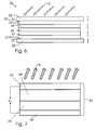
- FIGS. 1 and 2 illustrated embodiments show surface elements of the prior art, which are applied to a substrate layer 8.
- a transparent substrate layer 8 is used, on which a transparent front electrode layer 4 of a lighting layer 1 is applied.
- a luminescent layer 6 and, subsequently, a dielectric layer 7 are applied to the front electrode layer 4.
- the illumination layer 1 is terminated by a back electrode layer 5.
- a luminous voltage U L can be applied between the front electrode 4 and the baking electrode 5.
- this luminous voltage U L can be between 12 volts and 300 volts.
- lower and higher voltages are also conceivable.
- an insulating layer 3 for electrical / electronic separation of the illumination layer 1 and a still following heating layer 2 is applied, to which a ceramic layer 9 connects.
- the heating layer 2 is finally arranged, to which a heating voltage U H can be applied.
- the heating voltage U H can assume different voltages depending on the application, but is preferably in the range between 12 volts and 300 volts.
- a non-transparent substrate layer 8 is present, on the one side of the illumination layer 1 with the transparent front electrode 4 and the baking electrode 5, between which in turn a luminous layer 6 and a dielectric layer 7 are introduced.
- an insulating layer 3 is in turn arranged for the electrical / electronic separation of the illumination layer 1 and the heating layer 2.
- a ceramic layer 9 is also arranged in this embodiment, through which the heat generated by the heating layer 2 can be better released to the environment.
- those in the FIGS. 1 and 2 illustrated embodiments of the surface element according to the invention are prepared by screen printing, wherein the starting materials of the individual layers are present as pastes. It has proven useful to use the materials mentioned in the introduction of the individual layers, wherein advantageously the pastes for producing the individual layers all have nanoparticles.
- the substrate layer 2 made of a plastic, the front electrode layer 4 of PEDOT / PSS, the luminescent layer 6 of an organic solution, the dielectric layer 7 of barium titanad, the back electrode layer 5 of silver, the insulating layer 3 of PVC, the ceramic layer 9 of nanoceramics and the heating layer. 2 made of carbon nanotubes.
- 3 and 4 show two exemplary embodiments of an inventive surface element 10 for lighting and storing energy.
- Fig. 3 shows a surface element 10 with a transparent energy converter unit 20.
- a battery layer 60 is first arranged. Above this there is an illumination layer 40 and above it the energy converter unit 20.
- the surface element 10 is shown in a lighting mode.
- the light 18 emitted by the illumination layer 40 is shown in the form of arrows.
- the carrier element 100 is arranged on the side of the energy converter unit 20 as a transparent substrate layer. Such an arrangement is for example in Fig. 4 shown, but with a non-transparent energy converter unit 20. Reference numerals are not necessarily re-explained.
- the illumination layer 40 is formed with the energy conversion unit 20 as a combined layer.
- the support member 14 is disposed adjacent to the combined layer. It is also conceivable here for the carrier element 14 to be arranged adjacent to the battery layer 60. Depending on which side of the carrier element is arranged, the order in which the layers are printed changes.
- Fig. 5 shows an exemplary battery layer 60.
- a separator 66 including electrolyte is surrounded by two layers of printed substrate 64, 68. On one side there is a positive terminal 72, on the other side a negative terminal 74.
- the two printed substrate layers 64, 68 are surrounded by encapsulation layers 62, 70.
- Fig. 6 shows an exemplary energy converter layer 20. This is shown in the irradiation mode.
- Reference numeral 12 represents the incident light 12 in the form of arrows.
- a transparent encapsulation 22 On the side facing the incident light 12 is a transparent encapsulation 22.
- Adjacent to the encapsulation 22 facing the incident light 12 is a transparent front electronics with an electrode connection 25.
- Adjacent to the front electrode is a support structure 26, adjoining this a solar active material 28, adjacent thereto a transport layer 21, adjacent thereto a baking electrode 23.
- this baking electrode can be made transparent or non-transparent and has a minus connection 27.
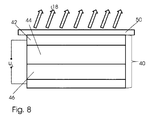
- Fig. 7 and Fig. 8 each show a layer structure of an illumination layer 40. This is shown in the illumination mode with emitted light 18.
- a front electrode layer 42 adjoining this a luminescent layer 44, adjoining this a dielectric layer 46 and adjacent thereto a back electrode layer 48.
- a voltage U L can be applied between front electrode layer 42 and back electrode layer 48.
- a carrier element 50 is shown, which is formed as a transparent substrate layer.
Landscapes
- Physics & Mathematics (AREA)
- Engineering & Computer Science (AREA)
- General Physics & Mathematics (AREA)
- Theoretical Computer Science (AREA)
- Manufacturing & Machinery (AREA)
- Electromagnetism (AREA)
- Electroluminescent Light Sources (AREA)
- Surface Heating Bodies (AREA)
- Resistance Heating (AREA)
Abstract
Die Erfindung betrifft ein Flächenelement zum Leuchten und Erzeugen sowie Speichern von Energie aufweisend einen Multilayer, der wenigstens eine Beleuchtungsschicht zum Leuchten, wenigstens eine Akkuschicht zum Speichern von Energie und wenigstens ein Trägerelement als Unterlage zum Aufdrucken der anderen Schichten umfasst, wobei die wenigstens eine Beleuchtungsschicht und die wenigstens eine Akkuschicht wenigstens abschnittsweise übereinander auf das wenigstens eine Trägerelement aufgedruckt sind.The invention relates to a surface element for lighting and generating and storing energy comprising a multilayer comprising at least one illumination layer for lighting, at least one battery layer for storing energy and at least one support element as a base for printing the other layers, wherein the at least one illumination layer and the at least one battery layer are at least partially printed one above the other on the at least one carrier element.
Description
Die Erfindung betrifft ein Flächenelement zum Leuchten und Speichern von Energie.The invention relates to a surface element for lighting and storing energy.
Althergebracht für Werbeanwendungen sind Litfasssäulen und Plakatwände. Auch wenn diese sich bereits über Jahrzehnte bewährt haben, mittels moderner Klebe- und Druckverfahren austauschbar sind, so hat sich im Zeitalter der digitalen Meiden eine starke Suche nach Alternativen eingestellt. Nun gibt es Leuchtbilder mit Neonröhren oder LEDs. In der Regel benötigen solche jedoch Strom- und Kabelanschlüsse, weisen ein hohes Gewicht auf und sind schwierig zu installieren. Zudem ist eine Änderung der Werbebotschaft nur sehr schwierig zu realisieren. Flachbildschirme und Beamer-Leinwände zieren mittlerweile auch viele Plätze und dienen der austauschbaren Werbeanwendung oder der Ankündigung von Veranstaltungen. Für Werbebotschaften ist es jedoch nicht immer notwendig, direkt einen kompletten Flachbildschirm bereitzustellen. Realisiert sind auch Standardsolarzellen mit LEDs und mittels Laser herausgeschnittenen Beschriftungen. Solche Produkte sind recht teuer, eintönig und schwer sowie mehrere Zentimeter dick.Traditional for advertising applications are advertising pillars and billboards. Although these have proven their worth over decades and are interchangeable by means of modern adhesive and printing processes, in the age of digital media a strong search for alternatives has come to an end. Now there are fluorescent pictures with neon tubes or LEDs. However, these usually require power and cable connections, are heavy and difficult to install. In addition, a change in the advertising message is very difficult to realize. Flat screens and beamer screens now adorn many places and serve the interchangeable advertising application or the announcement of events. For advertising messages, however, it is not always necessary to provide a complete flat screen directly. Also realized are standard solar cells with LEDs and laser-cut labels. Such products are quite expensive, monotonous and heavy as well as several centimeters thick.
Aus dem firmeninternen Stand der Technik ist ein Flächenelement zum Leuchten und Heizen bekannt. Es wird auf Anmeldung
Das Flächenelement zum Leuchten und Heizen besteht im Wesentlichen aus einem Multilayer, der wenigstens eine Beleuchtungsschicht und wenigstens eine Heizschicht sowie eine zwischen diesen angeordnete Isolierungsschicht und/oder Keramikschicht aufweist. Die wenigstens eine Beleuchtungsschicht besteht dabei aus einer transparenten Frontelektrodenschicht und einer Backelektrodenschicht mit dazwischen angeordneter Leuchtschicht und Dielektrikumsschicht. Dabei ist zwischen der Frontelektrodenschicht und der Backelektrodenschicht eine Leuchtspannung und an die wenigstens eine Heizschicht eine Heizspannung anlegbar.The surface element for lighting and heating essentially consists of a multilayer which has at least one illumination layer and at least one heating layer and an insulating layer and / or ceramic layer arranged between them. The In this case, at least one illumination layer consists of a transparent front electrode layer and a back electrode layer with a luminescent layer and dielectric layer arranged therebetween. In this case, a luminous voltage is applied between the front electrode layer and the back electrode layer and a heating voltage can be applied to the at least one heating layer.
Durch diese Ausgestaltung ist es ermöglicht, ein sehr breit einsetzbares Flächenelement zur Verfügung zu stellen, mit dessen Hilfe sowohl Leucht- als auch Heizfunktionen übernommen werden können. Dabei ist das Flächenelement in seiner geometrischen Form nicht auf eine ebene Fläche beschränkt. Vielmehr können auch Flächenelemente hergestellt werden, die eine gekrümmte Fläche beziehungsweise sogar eine mehrfach gekrümmte Fläche aufweisen. Vorteilhaft dabei ist insbesondere auch, dass solche Flächenelemente an räumliche Gegebenheiten vor Ort angepasst werden können und somit platzsparend installiert werden können. Insbesondere bei einem geringen Raumangebot ist eine solche Ausgestaltung eines erfindungsgemäßen Flächenelementes sehr vorteilhaft, da es räumlich nur sehr wenig Platz benötigt und keine separaten Beleuchtungs- und Heizeinrichtungen installiert werden müssen. Die Energieversorgung ist dabei in der Regel derart ausgestaltet, dass sowohl die Heizspannung als auch die Leuchtspannung in einem Bereich zwischen 12 Volt und 300 Volt liegt. Allerdings sind auch andere Spannungsbereiche denkbar. Die zu verwendenden Spannungen richten sich in der Regel nach dem Anwendungsbeispiel und den Dimensionen der Leucht- und Heizschicht.With this configuration, it is possible to provide a very wide usable surface element available, with the help of both lighting and heating functions can be adopted. In this case, the surface element is not limited in its geometric shape on a flat surface. Rather, it is also possible to produce surface elements which have a curved surface or even a surface that is curved several times. It is also advantageous in particular that such surface elements can be adapted to spatial conditions on site and thus can be installed to save space. Such a configuration of a surface element according to the invention is particularly advantageous in the case of a small amount of space, since it requires very little space in space and no separate lighting and heating devices have to be installed. The power supply is usually designed such that both the heating voltage and the lighting voltage is in a range between 12 volts and 300 volts. However, other voltage ranges are conceivable. The voltages to be used are usually based on the application example and the dimensions of the luminous and heating layers.
Grundsätzlich ist es möglich, ein erfindungsgemäßes Flächenelement auf jeglicher Art von Oberfläche aufzubringen, beispielsweise auf Oberflächen aus Glas, Papier, Plastik, Granit, Metall oder dergleichen. Insofern würden die einzelnen Schichten in der entsprechenden Reihenfolge auf die jeweilige Oberfläche aufgebracht, wobei die Beleuchtungsschicht die äußere Schicht bildet und in Richtung des Raumes angeordnet ist, der durch die Beleuchtungsschicht ausgeleuchtet werden soll. Die äußere zum auszuleuchtenden Raum hinweisende Schicht der Beleuchtungsschicht ist dabei die transparente Frontelektrodenschicht, auf der gegebenenfalls noch eine transparente Substratschicht zum Schutz der Frontelektrodenschicht aufgebracht ist.In principle, it is possible to apply a surface element according to the invention to any type of surface, for example to surfaces of glass, paper, plastic, granite, metal or the like. In this respect, the individual layers would be applied to the respective surface in the appropriate sequence, wherein the illumination layer forms the outer layer and is arranged in the direction of the space which is to be illuminated by the illumination layer. The outer layer of the illumination layer indicative of the space to be illuminated is the transparent front electrode layer on which, if appropriate, a transparent substrate layer for protecting the front electrode layer is applied.
Es ist allerdings auch möglich, das erfindungsgemäße Flächenelement mit seinen Schichten nicht direkt auf die zu beschichtende Oberfläche aufzubringen. Vielmehr kann die Beleuchtungsschicht und die Heizschicht auch auf eine Substratschicht aufgebracht werden, sodass ein folienartiges Flächenelement gegeben ist. Ein solches folienartiges Flächenelement ist in seiner Anwendung sehr breit einsetzbar, da es in seiner Ausgestaltung absolut biegsam ist und auf die verschiedensten Arten von Oberflächen aufbringbar ist. Daraus ergeben sich hervorragende Einsatzmöglichkeiten in vielen Bereichen des täglichen Lebens, wie beispielsweise beim Hausbau oder auch in der Automobilindustrie und/oder dergleichen.However, it is also possible not to apply the surface element according to the invention with its layers directly on the surface to be coated. Rather, the lighting layer and the heating layer are also applied to a substrate layer, so that a sheet-like surface element is given. Such a sheet-like surface element is very widely used in its application, since it is absolutely flexible in its design and can be applied to various types of surfaces. This results in excellent applications in many areas of daily life, such as in building or in the automotive industry and / or the like.
Besonders vorteilhaft ist es, wenn
- i) die Beleuchtungsschicht zwischen 8,05 µm und 120 µm stark ist, wobei vorzugsweise
- a) die transparente Frontelektrodenschicht zwischen 0,05 µm und 5 µm,
- b) die Backelektrodenschicht zwischen 4 µm und 45 µm,
- c) die Leuchtschicht zwischen 2 µm und 30 µm und
- d) die Dielektrikumsschicht zwischen 4 µm und 45 µm stark ist,
- ii) die Heizschicht zwischen 6 µm und 60 µm stark ist und/oder
- iii) die Isolierungsschicht zwischen 1 µm und 15 µm und die Keramikschicht (9) zwischen 3 µm und 30 µm stark ist.
- i) the illumination layer is between 8.05 μm and 120 μm thick, preferably
- a) the transparent front electrode layer between 0.05 μm and 5 μm,
- b) the baking electrode layer is between 4 μm and 45 μm,
- c) the luminescent layer between 2 microns and 30 microns and
- d) the dielectric layer is between 4 μm and 45 μm thick,
- ii) the heating layer is between 6 μm and 60 μm thick and / or
- iii) the insulating layer between 1 .mu.m and 15 .mu.m and the ceramic layer (9) between 3 .mu.m and 30 .mu.m thick.
Solche Schichten lassen sich mit herkömmlichen Verfahren in einfacher Weise herstellen und auf entsprechende Oberflächen aufbringen. Beispielhaft seien hier nur verschiedene Druckverfahren genannt, wie beispielsweise Siebdruck oder auch Offsetdruck.Such layers can be easily produced by conventional methods and applied to corresponding surfaces. By way of example, only different printing methods are mentioned here, for example screen printing or offset printing.
Um aber eine biegsame Folie herzustellen, die möglichst in vielen Anwendungsbereichen eingesetzt werden kann, hat es sich als besonders vorteilhaft erwiesen, dass die separate Substratschicht zwischen 10 µm und 1000 µm stark ist. Durch diese Ausgestaltung der Erfindung erhält man eine dünne Folie, welche maximal im Bereich von 1 mm stark ist und die auf entsprechenden Oberflächen angeordnet werden kann.However, in order to produce a flexible film which can be used in as many applications as possible, it has proven to be particularly advantageous that the separate substrate layer is between 10 .mu.m and 1000 .mu.m thick. By this embodiment of the invention, a thin film is obtained, which is maximum in the range of 1 mm thick and which can be arranged on corresponding surfaces.
Dabei hat es sich weiterhin bewährt, dass die Frontelektrodenschicht Silber-Nano-Wires, Carbon-Nano-Tubes, PEDOT/PSS Materialien (Materialien aus mit Polystyrolsulfonat dotiertem Poly-3,4-ethylendioxythiophen), ITO-Pigmente (Pigmente aus Indiumzinnoxid), Zinkoxid, Aluminiumoxid, organische Lösungen, Emulsierer, Verdicker, Verdünner, Konditionierer, Viskositätsmittel, Kleber, Anti-Oxidanzmittel und/oder dergleichen Materialien enthält. Solche Materialien eignen sich besonders gut für die Anwendung als Frontelektrodenschicht, da sie sehr lichtdurchlässig sind, und somit nur ein sehr geringer Anteil des durch die Leuchtschicht erzeugten Lichtes von der Frontelektrodenschicht absorbiert wird. Das von der Leuchtschicht emittierte Licht kann somit im Wesentlichen verlustfrei die Frontelektrodenschicht passieren und zur Ausleuchtung des Raumes genutzt werden.It has further proven that the front electrode layer silver nano-Wires, carbon nanotubes, PEDOT / PSS materials (materials of poly-3,4-ethylenedioxythiophene doped with polystyrene sulfonate), ITO pigments (pigments of indium tin oxide), Zinc oxide, alumina, organic solutions, emulsifiers, thickeners, thinners, conditioners, viscosity agents, adhesives, anti-oxidants and / or the like materials. Such materials are particularly well suited for use as a front electrode layer, since they are very transparent, and thus only a very small portion of the through the luminescent layer generated light is absorbed by the front electrode layer. The light emitted by the luminescent layer can thus pass through the front electrode layer essentially without loss and can be used to illuminate the room.
Da es bei der Backelektrodenschicht nicht notwendig ist, dass diese transparent ist, enthält die Backelektrodenschicht Silber, Kupfer, Zinn, Zink, Carbon, PEDOT/PSS Materialien (Materialien aus mit Polystyrolsulfonat dotiertem Poly-3,4-ethylendioxythiophen), Zinkoxid, Aluminiumoxid, organische Lösungen, Emulsierer, Verdicker, Verdünner, Konditionierer, Viskositätsmittel, Kleber, Anti-Oxidantmittel und/oder dergleichen Materialien. Die Backelektrodenschicht und die Frontelektrodenschicht weisen durch die Materialeigenschaften der eingesetzten Materialien die für die Nutzung als Elektrode notwendigen elektrischen und/oder elektronischen Eigenschaften auf, sodass die Beleuchtungsschicht mit diesen Elektroden sehr effizient betrieben werden kann.Since it is not necessary for the back electrode layer to be transparent, the back electrode layer contains silver, copper, tin, zinc, carbon, PEDOT / PSS materials (polystyrenesulfonate doped poly-3,4-ethylene dioxythiophene materials), zinc oxide, alumina, organic solvents, emulsifiers, thickeners, thinners, conditioners, viscosity agents, adhesives, anti-oxidants and / or the like materials. Due to the material properties of the materials used, the back electrode layer and the front electrode layer have the necessary electrical and / or electronic properties for use as electrodes, so that the illumination layer can be operated very efficiently with these electrodes.
Zur Verwendung der Leuchtschicht haben sich insbesondere Nano-Zinksulfid, Europium, Siliziumnitrid, organische Lösungen, Emulsierer, Verdicker beziehungsweise Verdünner, Konditionierer, Viskositätsmittel, Kleber, Anti-Oxidantmittel und/oder dergleichen Materialien als besonders sinnvoll erwiesen. Insbesondere haben sich hier organische Lösungen als besonders geeignet erwiesen, da diese sehr energieeffizient, beispielsweise als organische Leuchtdioden, das entsprechende Licht zur Ausleuchtung des Raumes erzeugen. Hiermit kann die Leuchtschicht beziehungsweise die Beleuchtungsschicht sehr energieeffizient betrieben werden, wobei annähernd die gesamte elektrische Energie, die über die Leuchtspannung der Beleuchtungsschicht zugeführt wird, in Lichtenergie umgewandelt wird.In particular, nano-zinc sulfide, europium, silicon nitride, organic solutions, emulsifiers, thickeners or thinners, conditioners, viscosity agents, adhesives, anti-oxidant agents and / or the like materials have proven particularly useful for the use of the luminescent layer. In particular, organic solutions have proved to be particularly suitable here, since they produce the corresponding light for illuminating the room in a very energy-efficient manner, for example as organic light-emitting diodes. Hereby, the luminescent layer or the illumination layer can be operated very energy-efficiently, wherein approximately the entire electrical energy that is supplied via the luminous voltage of the illumination layer is converted into light energy.
Die Dielektrikumsschicht enthält Bariumtitanad, Isoliermittel, organische Lösungen, Emulsierer, Verdicker beziehungsweise Verdünner, Konditionierer, Viskositätsmittel, Kleber, Anti-Oxidantmittel und/oder dergleichen Materialien.The dielectric layer contains barium titanate, insulators, organic solvents, emulsifiers, thickeners, conditioners, viscosity agents, adhesives, anti-oxidant agents, and / or similar materials.
Die Heizschicht enthält im Wesentlichen Carbon-Nano-Tubes, organische Lösungen, Emulsierer, Verdicker, Verdünner, Konditionierer, Viskositätsmittel, Kleber, Anti-Oxidantmittel und/oder dergleichen Materialien. Die hier als Heizschicht eingesetzten Materialien wandeln nahezu 100 % der über die Heizspannung eingespeisten elektrischen Energie in Wärme um. Somit kann durch das erfindungsgemäße Flächenelement eine Maximaltemperatur oberhalb von 200° (523 K) erzeugt werden.The heating layer essentially comprises carbon nanotubes, organic solutions, emulsifiers, thickeners, thinners, conditioners, viscosity agents, adhesives, anti-oxidant agents and / or similar materials. The materials used here as a heating layer convert almost 100% of the electrical energy fed in via the heating voltage into heat. Thus, a maximum temperature above 200 ° (523 K) can be generated by the surface element according to the invention.
Zwischen der Heizschicht und der Beleuchtungsschicht ist vorzugsweise noch eine Isolierungsschicht angeordnet, um eine elektronische/elektrische Trennung zwischen diesen Schichten zu erreichen. Die Isolierungsschicht enthält im Wesentlichen PET, PVC, organische Lösungen, Emulsierer, Verdicker, Verdünner, Konditionierer, Viskositätsmittel, Kleber, Anti-Oxidantmittel und/oder dergleichen Materialien.Between the heating layer and the illumination layer is preferably still an insulating layer arranged to achieve an electronic / electrical separation between these layers. The insulation layer essentially comprises PET, PVC, organic solutions, emulsifiers, thickeners, thinners, conditioners, viscosity agents, adhesives, anti-oxidant agents and / or similar materials.
Ferner kann zwischen Beleuchtungsschicht und Heizschicht noch eine Keramikschicht vorgesehen sein. Die Keramikschicht enthält im Wesentlichen Nano-Keramiken, organische Lösungen, Emulsierer, Verdicker, Verdünner, Konditionierer, Viskositätsmittel, Kleber, Anti-Oxidantmittel und/oder dergleichen Materialien und dient aufgrund ihrer guten Wärmeleitfähigkeit im Wesentlichen dazu, die durch das Heizelement erzeugte Wärme besser an die Raumumgebung abzugeben.Furthermore, a ceramic layer may be provided between the illumination layer and the heating layer. The ceramic layer substantially contains nano-ceramics, organic solutions, emulsifiers, thickeners, thinners, conditioners, viscosity agents, adhesives, anti-oxidants and / or the like materials and, due to its good thermal conductivity, essentially serves to better heat the heat generated by the heating element to leave the room environment.
Die Substratschicht enthält im Wesentlichen Glas, Papier, Kunststoff, Granit, Metall und/oder dergleichen Materialien. Aus solchen Materialien können sehr dünne Substratschichten hergestellt werden, sodass Flächenelemente in Form von vorzugsweise biegsamen Folien für alle möglichen Anwendungen in einfacher Weise hergestellt werden können. Solche biegsame Folien können auf vielen möglichen Oberflächen angeordnet und dort zum Heizen und Ausleuchten von Räumen genutzt werden.The substrate layer essentially contains glass, paper, plastic, granite, metal and / or similar materials. Very thin substrate layers can be produced from such materials, so that surface elements in the form of preferably flexible films can be produced in a simple manner for all possible applications. Such flexible films can be arranged on many possible surfaces and used there for heating and lighting of rooms.
Ferner sind auch Schalter und/oder Regeleinrichtungen vorgesehen, mit denen die Heizspannung und die Leuchtspannung ein- und ausschaltbar und regelbar sind, wobei die Schalter und/oder Regeleinrichtungen als externe Elemente oder aber als interne integrierte oder externe Elemente, wie beispielsweise Helligkeitsmesser, Bewegungssensoren, Zeitschaltuhren, Dimmer und/oder Temperaturmesser und/oder dergleichen, ausgebildet sind.Furthermore, switches and / or regulating devices are provided with which the heating voltage and the lighting voltage can be switched on and off and regulated, wherein the switches and / or control devices as external elements or as internal integrated or external elements, such as brightness meter, motion sensors, Timers, dimmers and / or temperature and / or the like are formed.
Vorteilhafterweise ist die Leuchtschicht zum Leuchten mit einer Lichtstärke von bis zu 500 Cd/m2 vorzugsweise zum flimmer- und/oder blendfreien und besonders bevorzugt zum Leuchten in verschiedenen Farben ausgebildet.Advantageously, the luminescent layer is designed for illumination with a light intensity of up to 500 Cd / m 2, preferably for flicker and / or glare-free and particularly preferably for illumination in different colors.
Denkbar ist, dass die Heizschicht zum Heizen bis maximal 523 K ausgebildet ist.It is conceivable that the heating layer is designed for heating up to 523 K maximum.
Grundsätzlich können die einzelnen Schichten des erfindungsgemäßen Flächenelementes zum Leuchten und zum Heizen als Paste vorliegen, welche beispielsweise mit einem Siebdruckverfahren auf jegliches Material aufgetragen werden, welches nach Bedruckung mit den Pasten leuchtet und heizt. Der Vorteil des erfindungsgemäßen Flächenelementes ist, dass die Beschichtungen absolut biegsam sind und eine Dicke von unter einem Millimeter erlauben. Die Größe der Beschichtung ist dabei nicht begrenzt. Ein weiterer Vorteil ist, dass das Licht sehr gleichmäßig blend- und flimmerfrei bei sehr geringem Stromverbrauch in definierbaren Farben leuchtet. Es sind Leuchtstärken bis zu 500 Cd/m2 denkbar. Die Heizbeschichtung setzt nahezu 100 % der elektrischen Energie in Wärme um und kann Maximaltemperaturen oberhalb von 200° C (523 K) erzeugen. Ebenso ist das entwickelte Flächenelement zum Heizen und Leuchten für Indoor- und Outdoorbenutzung geeignet. Es verträgt Nässe und Feuchtigkeit. Auch unter Wasser kann die Beschichtung eingesetzt werden. Der Temperaturbereich kann zwischen minus 45° C (228 K) und plus 150° C (423 K) liegen. Die Betriebsdauer ist extrem lange und liegt derzeit bei mehreren 1000 Stunden. Der Vorteil des erfindungsgemäßen Flächenelementes liegt weiter im optimierten Materialeinsatz der Energie umwandelnden Schichten. Dadurch ist es erstmals möglich, derartige Kombiprodukte mittels eines einfachen Herstellungsverfahrens, beispielsweise eines Siebdruckprozesses herzustellen. Durch die Kombination von Heiz- und Leuchtfunktionen sind Gewichtsvorteile und Preisvorteile immer dann vorhanden, wenn man Licht und Heizung an einem Ort einsetzen will oder muss.In principle, the individual layers of the surface element according to the invention for illumination and for heating can be in the form of paste, which are applied to any material, for example by a screen printing process, which lights and heats when printed with the pastes. The advantage of the surface element according to the invention is that the coatings are absolutely flexible and allow a thickness of less than one millimeter. The size of the coating is not limited. Another advantage is that the light shines very uniformly glare and flicker-free with very low power consumption in definable colors. Luminous intensities of up to 500 Cd / m 2 are conceivable. The heating coating converts nearly 100% of the electrical energy into heat and can produce maximum temperatures above 200 ° C (523 K). Likewise, the developed surface element is suitable for heating and lighting for indoor and outdoor use. It can withstand moisture and moisture. Even under water, the coating can be used. The temperature range can be between minus 45 ° C (228 K) and plus 150 ° C (423 K). The operating time is extremely long and is currently several 1000 hours. The advantage of the surface element according to the invention lies in the optimized use of materials of the energy-converting layers. This makes it possible for the first time to produce such combination products by means of a simple production method, for example a screen printing process. The combination of heating and lighting functions, weight advantages and price advantages are always present when you want to use light and heating in one place or must.
Der Erfindung liegt die Aufgabe zugrunde, ein Flächenelement zum Leuchten und Speichern von Energie zu schaffen, welches leicht, kostengünstig und sehr dünn ist.The invention has for its object to provide a surface element for lighting and storing energy, which is lightweight, inexpensive and very thin.
Gelöst wird diese Aufgabe durch ein Flächenelement zum Leuchten und Speichern von Energie mit sämtlichen Merkmalen des Patentanspruches 1. Ferner wird die Aufgabe auch durch ein Verfahren zum Herstellen eines Flächenelements mit sämtlichen Merkmalen des Patentanspruches 11 gelöst. Vorteilhafte Ausgestaltungen finden sich in den Unteransprüchen.This object is achieved by a surface element for lighting and storing energy with all the features of
Das erfindungsgemäße Flächenelement zum Leuchten und Speichern von Energie weist einen Multilayer auf, der wenigstens eine Beleuchtungsschicht zum Leuchten, wenigstens eine Akkuschicht zum Speichern von Energie und wenigstens ein Trägerelement als Unterlage zum Aufdrucken der anderen Schichten umfasst, wobei die wenigstens eine Beleuchtungsschicht und die wenigstens eine Akkuschicht wenigstens abschnittsweise übereinander auf das wenigstens eine Trägerelement aufgedruckt sind.The surface element according to the invention for illuminating and storing energy has a multilayer comprising at least one illumination layer for lighting, at least one battery layer for storing energy and at least one carrier element as a base for printing the other layers, wherein the at least one illumination layer and the at least one battery layer are at least partially printed one above the other on the at least one carrier element.
Unter einem Multilayer ist dabei eine Folge von mehreren Schichten zu verstehen. Als Trägeelement ist eine Schichtunterlage aus Keramikvlies, PET-Folie, Papier, Spezialfolien wie beispielsweise Capton, Navion von Dupont, Acryl, Plexiglas, Makrolon, Glas, Granit, Metall oder dergleichen. Dabei ist sowohl denkbar, dass das Trägerelement der Akkuschicht zugewandt ist, als auch, dass das Trägerelement der Beleuchtungsschicht zugewandt ist. Vorteilhaft sind die Schichten flächendeckend direkt übereinander angeordnet. Denkbar ist jedoch eine mittelbare Anordnung mit wenigstens einer Zwischenschicht. Möglich sind jedoch beliebig viele Schichten. Vorteilhaft ist das Trägerelement als rechteckige Schicht ausgebildet. Jedoch sind auch beliebige andere Formen denkbar. Besonders vorteilhaft ist das Trägerelement als Folie ausgebildet. Dies ist vorteilhaft, da sich auf diese Weise ein besonders leichter Aufbau ergibt, der an jedem beliebigen Untergrund passbar ist.A multilayer is to be understood as a sequence of several layers. As a supporting element is a layer backing made of ceramic fleece, PET film, paper, special films such as Capton, Navion of Dupont, acrylic, Plexiglas, Makrolon, glass, granite, metal or the like. It is conceivable that the carrier element faces the battery layer, as well as that the carrier element faces the illumination layer. The layers are advantageously arranged directly one above the other across the board. However, an indirect arrangement with at least one intermediate layer is conceivable. However, any number of layers are possible. Advantageously, the carrier element is designed as a rectangular layer. However, any other shapes are conceivable. Particularly advantageously, the carrier element is designed as a film. This is advantageous because in this way results in a particularly lightweight construction, which is passable on any surface.
Ferner ist denkbar, dass das Trägerelement transparent ausgebildet ist. Dies ist besonders vorteilhaft, um durchlässig für das Licht einer Leuchtschicht zu sein. Denkbar ist jedoch auch ein nicht transparentes Trägerelement.Furthermore, it is conceivable that the carrier element is transparent. This is particularly advantageous in order to be transparent to the light of a luminescent layer. However, a non-transparent carrier element is also conceivable.
Denkbar ist, dass die Beleuchtungsschicht eine gesamtflächige monochrome Beleuchtung darstellt. Vorteilhaft ist eine segmentierte Beleuchtungsschicht, der wenigstens ein Teilflächensegment zum Leuchten anregbar ist. Dabei ist denkbar, dass ein Teilflächensegment die Form einer Werbeabbildung, eines Buchstabensegmentes oder Zeichensegmentes aufweist.It is conceivable that the illumination layer represents a total area monochrome illumination. Advantageously, a segmented illumination layer, which is at least a partial surface segment for illumination excitable. It is conceivable that a partial surface segment has the form of an advertising image, a letter segment or character segment.
Auf diese Weise ist das Segment als leuchtendes Werbeelement oder Hinweiselement verwendbar. Insbesondere ist eine Zusammensetzung der Beleuchtungsschicht aus mehreren separat ansteuerbaren Leuchtsegmenten denkbar. Dies ist vorteilhaft, da auf diese Weise das Flächenelement verschiedene Leuchtformen darstellen kann. Zum Ansteuern ist dabei eine Elektronikplatine denkbar, die als weitere Schicht angrenzend zu der Beleuchtungsschicht angeordnet ist und Kontakte zu den Einzelnen Teilflächensegmenten der Beleuchtungsschicht aufweist. Dies ist vorteilhaft, da auf diese Weise die Steuerung direkt in das Flächenelement eingebaut ist.In this way, the segment can be used as a luminous advertising element or reference element. In particular, a composition of the illumination layer of a plurality of separately controllable light segments is conceivable. This is advantageous because in this way the surface element can represent different forms of light. For driving an electronic circuit board is conceivable, which is arranged as a further layer adjacent to the illumination layer and having contacts to the individual partial surface segments of the illumination layer. This is advantageous because in this way the controller is installed directly in the surface element.
In einer weiteren vorteilhaften Ausführungsform weist die wenigstens eine Beleuchtungsschicht eine Frontelektrodenschicht und eine Backelektrodenschicht mit dazwischen angeordneter Leuchtschicht und Dielektrikumsschicht auf, wobei zwischen Frontelektrodenschicht und Backeletrodenschicht eine Leuchtspannung anlegbar ist. Vorteilhafte Materialien für die Fronelektrodenschicht, die Backelektrodenschicht, die Leuchtschicht sowie die Dielektrikumsschicht entsprechen den Materialien dieser Schichten bei dem Flächenelement zum Leuchten und Heizen. Auch vorteilhafte Dicken dieser Schichten entsprechen den vorteilhaften Dicken bei dem Flächenelement zum Leuchten und Heizen. Dieser Vierschichtaufbau ist besonders vorteilhaft. Zum effektiven Ausnutzen des Elektrolumineszenzeffektes dient die Dielektrikumsschicht zum Anpassen einer Kapazität. Besonders bekannt ist der Elektrolumineszenzeffekt an Zinksulfid, das durch eine hochfrequente Wechselspannung zum Leuchten anregbar ist. Durch die Frontelektrodenschicht und die Backelektrodenschicht kann die Wechselspannung auf die Leuchtschicht übertragen werden. Denkbar ist, dass beide Schichten nur einen Anschluss aufweisen, so dass eine von außen angelegte Wechselspannung effektiv übertragen wird. Dies ist vorteilhaft aufgrund der Einfachheit. Vorteilhaft ist jedoch denkbar, dass beispielsweise eine Platine angrenzend zu der Backelektrodenschicht angeordnet ist, die eine Auswahl der zu steuernden Leuchtsegmente der Leuchtschicht erlaubt, wobei jedoch die Frontelektrodenschicht der verschiedenen Leuchtsegmente miteinander in Verbindung steht. Das Flächenelement ist jedoch auf die genannten Varianten beschränkt.In a further advantageous embodiment, the at least one illumination layer has a front electrode layer and a back electrode layer with a luminescent layer and dielectric layer arranged therebetween, wherein a luminous voltage can be applied between the front electrode layer and the backplate layer. Advantageous materials for the Fronelektrodenschicht, the back electrode layer, the luminescent layer and the dielectric layer correspond to the materials of these layers in the surface element for lighting and heating. Advantageous thicknesses of these layers correspond to the advantageous thicknesses in the surface element for lighting and heating. This four-layer structure is particularly advantageous. To effectively exploit the electroluminescent effect, the dielectric layer serves to adjust a capacitance. Particularly well known is the electroluminescent effect of zinc sulfide, which can be excited by a high-frequency AC voltage to shine. The alternating voltage can be transmitted to the luminescent layer through the front electrode layer and the back electrode layer. It is conceivable that both layers have only one connection, so that an externally applied AC voltage is effectively transmitted. This is advantageous because of the simplicity. Advantageously, however, it is conceivable that, for example, a circuit board is arranged adjacent to the baking electrode layer, which allows selection of the light segments to be controlled of the luminescent layer, but wherein the front electrode layer of the different light segments is in communication. However, the surface element is limited to the variants mentioned.
In einer weiteren vorteilhaften Ausführungsform umfasst das Flächenelement weiterhin eine Energiewandlereinheit zum Umwandeln von eingestrahlter Lichtenergie in elektrische Energie. Dies ist vorteilhaft, da auf diese Weise beispielsweise eingestrahltes Sonnenlicht als elektrische Energie in der Akkuschicht gespeichert werden kann und anschließend zum Beleuchten der Beleuchtungsschicht Verwendung finden kann.In a further advantageous embodiment, the surface element further comprises an energy conversion unit for converting irradiated light energy into electrical energy. This is advantageous because in this way, for example, irradiated sunlight can be stored as electrical energy in the battery layer and can then be used to illuminate the illumination layer.
Bei einer weiteren vorteilhaften Ausführungsform ist die Energiewandlereinheit als transparente Schicht ausgebildet, insbesondere derart, dass übereinander auf die wenigstens eine Akkuschicht mittelbar oder unmittelbar die wenigstens eine Beleuchtungsschicht folgt und auf die wenigstens eine Beleuchtungsschicht über oder unmittelbar die wenigstens eine Energiewandlereinheit folgt. Dies ist vorteilhaft, da auf diese Weise die Energiewandlereinheit dem eingestrahlten Licht zugewandt werden kann. Da die Energiewandlerschicht transparent ausgebildet ist, kann sie bei Abnahme des einstrahlenden Lichtes zum Beispiel in der Abenddämmerung als durchlässige Schicht für das Licht der Beleuchtungsschicht Verwendung finden. Dabei ist denkbar, dass eine Durchkontaktierung zwischen Energiewandlerschicht und Akkuschicht durch die Beleuchtungsschicht hindurch das Übertragen der in der Energiewandlerschicht erzeugten elektrischen Schicht in die Akkuschicht ermöglicht. Der weitere Kontraktierung ermöglicht vorteilhaft das Freisetzen der in der Akkuschicht gespeicherten Energie für die Anregung der Beleuchtungsschicht.In a further advantageous embodiment, the energy conversion unit is embodied as a transparent layer, in particular such that the at least one battery layer directly or indirectly follows the at least one illumination layer and the at least one illumination layer follows the at least one energy conversion unit. This is advantageous because in this way the energy conversion unit can be turned towards the incident light. Since the energy conversion layer is transparent, it can use as a transmissive layer for the light of the illumination layer, for example, at dusk, when the incident light decreases Find. It is conceivable that a via between the energy converter layer and the battery layer through the illumination layer allows the transfer of the electrical layer generated in the energy converter layer into the battery layer. The further contracting advantageously makes it possible to release the energy stored in the battery layer for the excitation of the illumination layer.
In einer weiteren vorteilhaften Ausführungsform ist die wenigstens eine Energiewandlereinheit nicht transparent ausgebildet, bevorzugt derart, dass wenigstens eine kombinierte Schicht des Flächenelementes aus einem als Beleuchtungsschicht ausgebildeten Teilflächenbereich und einem als Energiewandlereinheit ausgebildeten Teilflächenbereich ausgebildet ist, besonders bevorzugt derart, dass übereinander auf die wenigstens eine Akkuschicht mittelbar oder unmittelbar wenigstens die eine kombinierte Schicht folgt. Die Teilflächenbereiche der Energiewandlereinheit und der Beleuchtungsschicht sind dabei in Erstreckungsrichtung der Schichten nebeneinander angeordnet. Dies ist besonders vorteilhaft, da auf diese Weise keine weitere Schicht angrenzend zu der Beleuchtungsschicht angeordnet ist, welche das abstrahlende Licht dämpfen würde. Weiterhin sind firmenintern bekannte Energiewandlereinheiten, die nicht transparent ausgebildet sind, effektiver und weisen einen größeren Wirkungsgrad gegenüber transparenten Energiewandlereinheiten auf. Nachteilig dabei ist jedoch, dass nicht die ganze Fläche des Flächenelementes für die Energiewandlereinheit und die Beleuchtungsschicht zur Verfügung steht. Vorteilhaft ist jedoch, dass die Akkuschicht sowohl angrenzend zu der Energiewandlerschicht als auch angrenzend zu der Beleuchtungsschicht anordbar ist, was in beiden Fällen ein besseren Energietransport ermöglicht.In a further advantageous embodiment, the at least one energy converter unit is non-transparent, preferably such that at least one combined layer of the surface element is formed from a partial surface region designed as an illumination layer and a partial surface region designed as an energy converter unit, particularly preferably such that one over the other at least one battery layer directly or indirectly followed by at least one combined layer. The partial surface areas of the energy conversion unit and the illumination layer are arranged side by side in the extension direction of the layers. This is particularly advantageous, since in this way no further layer is arranged adjacent to the illumination layer which would attenuate the emitting light. Furthermore, internally known energy converter units that are not transparent, more effective and have a greater efficiency over transparent energy converter units. The disadvantage here is that not the entire surface of the surface element is available for the energy conversion unit and the illumination layer. It is advantageous, however, that the battery layer can be arranged both adjacent to the energy converter layer and adjacent to the illumination layer, which in both cases enables better energy transport.
In einer weiteren vorteilhaften Ausführungsform umfasst die Energiewandlereinheit übereinander wenigstens eine transparente Frontelektrodenschicht und/oder danach mittelbar oder unmittelbar wenigstens eine Trägerstrukturschicht zur Stabilisierung des Flächenelementes und/oder danach mittelbar oder unmittelbar wenigstens eine Schicht solaraktives Material und/oder danach mittelbar oder unmittelbar wenigstens eine Transportschicht und/oder danach mittelbar oder unmittelbar wenigstens eine Backelektrodenschicht und/oder danach mittelbar oder unmittelbar wenigstens eine Verkapselungsschicht, wobei zwischen transparenter Frontelektrodenschicht und Backelektrodenschicht vorteilhaft eine Spannung anlegbar ist. Denkbar ist, dass dabei auf die Transportschicht und die Trägerstrukturschicht verzichtet wird. Dies ist vorteilhaft, da auf diese Weise eine besonders dünne Ausführungsform möglich ist. Nachteilig ist die jedoch, da die Transportschicht eine Aufrechterhaltung der Ladungstrennung besonders gute Eigenschaften aufweist. Zudem ist es denkbar, dass das solaraktive Material ohne eine stabilisierende Trägerstrukturschicht seine Wirkung einbüßt. Für die Trägerstrukturschicht sind Gläser, Plexiglas, Metallfolien, Plastikfolien und ähnliche flexible bzw. starre Substrate denkbar. Für die Transportschicht sind negative und positive Ausbildungen aus organischen und anorganischen Stoffen denkbar. Sie haben die Aufgabe, die Elektronen besser zu transportieren.In a further advantageous embodiment, the energy conversion unit comprises one another at least one transparent front electrode layer and / or thereafter directly or indirectly at least one support structure layer for stabilizing the surface element and / or thereafter directly or indirectly at least one layer of solar active material and / or thereafter directly or indirectly at least one transport layer and / or thereafter indirectly or directly at least one baking electrode layer and / or thereafter directly or indirectly at least one encapsulation layer, wherein a voltage can advantageously be applied between the transparent front electrode layer and the baking electrode layer. It is conceivable that the transport layer and the carrier structure layer are dispensed with. This is advantageous because in this way a particularly thin embodiment possible is. The disadvantage, however, is that the transport layer has a maintenance of charge separation particularly good properties. In addition, it is conceivable that the solar-active material without a stabilizing support structure layer loses its effect. For the support structure layer glasses, Plexiglas, metal foils, plastic films and similar flexible or rigid substrates are conceivable. For the transport layer, negative and positive forms of organic and inorganic substances are conceivable. Their job is to transport the electrons better.
Vorteilhaft ist die Verkapselung als Isolationsschicht ausgebildet.Advantageously, the encapsulation is formed as an insulating layer.
Die zur Backelektrode angrenzende Verkapselung weist vorteilhaft eine Dicke zwischen 500 Nanometer und 250 Mikrometer auf. Die Backelektrode weist vorteilhaft eine Dicke zwischen 100 Nanometer und 15 Mikrometer auf. Die Transportschicht weist vorteilhaft eine Dicke zwischen 50 Nanometer und 5 Mikrometer auf. Das solaraktive Material weist vorteilhaft eine Dicke zwischen 50 Nanometer und 5 Mikrobeter auf. Die Trägerstruktur weist vorteilhaft eine Dicke zwischen 100 Nanometer und 5 Mikrobeter auf. Die Frontelektrode weist vorteilhaft eine Dicke zwischen 100 Nanometer und 5 Mikrometer auf. Die zur Frontelektrode angrenzende Verkapselung weist vorteilhaft eine Dicke zwischen 20 und 250 Mirkometer auf.The encapsulation adjoining the baking electrode advantageously has a thickness of between 500 nanometers and 250 micrometers. The baking electrode advantageously has a thickness of between 100 nanometers and 15 micrometers. The transport layer advantageously has a thickness of between 50 nanometers and 5 micrometers. The solar active material advantageously has a thickness between 50 nanometers and 5 microbeter. The support structure advantageously has a thickness of between 100 nanometers and 5 microbeters. The front electrode advantageously has a thickness of between 100 nanometers and 5 micrometers. The encapsulation adjacent to the front electrode advantageously has a thickness of between 20 and 250 micrometers.
In einer weiteren vorteilhaften Ausführungsform weist die Akkuschicht wenigstens zwei bedruckte Substratschichten, dazwischen wenigstens einen Separator mit einem Elektrolyten und an den Außenseiten je wenigstens eine Verkapselungsschicht auf. Vorteilhaft ist die Verkapselungsschicht jeweils als Isolationsschicht ausgebildet. Die Substratschichten sind vorteilhaft aus einem Folienmaterial ausgebildet. Denkbar sind jedoch beliebige Materialien, die auch für das Trägerelement in Frage kommen. Als Materialien für die Akkuschicht sind u. a. Graphene, Grafit, organische Lösungen, Emulgierer, Verdicker oder Verdünner, Konditionierer, Viskositätsmittel, Kleber sowie Antioxidantmittel denkbar. Die Akkuschicht ist als Superkondensator, auch Ultrakondensator genannt, ausgebildet.In a further advantageous embodiment, the battery layer has at least two printed substrate layers, at least one separator with an electrolyte between them, and at least one encapsulation layer on each of the outer sides. Advantageously, the encapsulation layer is formed in each case as an insulating layer. The substrate layers are advantageously formed from a foil material. However, any materials are conceivable which also come into question for the carrier element. As materials for the Akkuschicht u. a. Graphene, graphite, organic solutions, emulsifiers, thickeners or thinners, conditioners, viscosity agents, adhesives and antioxidants conceivable. The battery layer is designed as a supercapacitor, also called an ultracapacitor.
In einer weiteren vorteilhaften Ausführungsform ist ein Helligkeitssensor, bevorzugt mit weiteren Regeleinheiten in dem Flächenelement integriert. Dies ist vorteilhaft, da auf diese Weise zwischen Akkuladungsbetrieb durch eine Energieumwandlerschicht und Leuchtbetrieb der Beleuchtungsschicht in Abhängigkeit von der Helligkeit automatisch umgeschaltet werden kann.In a further advantageous embodiment, a brightness sensor, preferably integrated with further control units in the surface element. This is advantageous since in this way it is possible to automatically switch over between battery charge operation by means of an energy converter layer and lighting operation of the illumination layer as a function of the brightness.
In einer weiteren vorteilhaften Ausführungsform sind die Verkapselungsschichten als Isolati-onsschichten ausgebildet und/oder das Flächenelement weist wenigstens eine weitere Zwischenschicht auf, bevorzugt ausgebildet als Isolationsschicht, als flexibles Substrat, als starres Substrat oder als gedruckte oder ungedruckte Elektronikschicht. Je nach Verwendungszweck können diese weiteren Schichten vorteilhaft angepasst, hinzugefügt oder weggelassen werden.In a further advantageous embodiment, the encapsulation layers are formed as insulation layers and / or the surface element has at least one further intermediate layer, preferably formed as an insulation layer, as a flexible substrate, as a rigid substrate or as a printed or unprinted electronics layer. Depending on the intended use, these additional layers can advantageously be adapted, added or omitted.
In einer weiteren vorteilhaften Ausführungsform ist das Flächenelement als Werbeschild, sowohl indoor als auch outdoor und/oder als Hinweisschild, z. B. als Verkehrsschild oder als Sicherheitsschild oder für einen Notausgang und/oder als Zuganzeigetafel ausgebildet. Jedoch ist die Verwendung nicht darauf beschränkt.In a further advantageous embodiment, the surface element as an advertising sign, both indoor and outdoor and / or as a sign, z. B. designed as a road sign or as a security shield or for an emergency exit and / or as Zuganzeigetafel. However, the use is not limited thereto.
Weiterhin wird die Aufgabe erfindungsgemäß auch von einem Verfahren zum Herstellen eines Flächenelementes gelöst, wobei wenigstens eine der Schichten mittels Siebdruck auf das Trägerelement aufgedruckt wird. Der Vorteil des Siebdruckverfahrens ist, dass die optimalen Schichtdicken in der gewünschten Höhe sehr schnell aufgetragen werden können. Geschwindigkeiten von bis zu 400 m2 pro Stunde sind mit der entsprechenden Druckmaschine möglich.Furthermore, the object is also achieved by a method for producing a surface element, wherein at least one of the layers is printed by screen printing on the carrier element. The advantage of the screen printing process is that the optimum layer thicknesses can be applied very quickly at the desired height. Speeds of up to 400 m 2 per hour are possible with the corresponding printing press.
Als Materialien für die Einzelschichten der Energiewandlerschicht sind aktive Schichten, z. B. aus CEGS, CZTS, Peroskite, CsSnl 3 und andere organische sowie anorganische Schichten vorteilhaft denkbar.As materials for the individual layers of the energy converter layer active layers, for. B. from CEGS, CZTS, peroskites,
Weiterhin ist auch wenigstens eine Keramikschicht als Zwischenschicht vorteilhaft denkbar. Besonders vorteilhaft besteht eine Keramikschicht aus Nanokeramiken, organischen Lösungen, Emulgierer, Verdicker, Verdünnern, Konditionierern, Viskositätsmitteln, Klebern, Antioxidantmitteln und/oder anderen Stoffen.Furthermore, at least one ceramic layer as an intermediate layer is advantageously conceivable. Particularly advantageous is a ceramic layer of nanoceramics, organic solutions, emulsifiers, thickeners, thinners, conditioners, viscosity agents, adhesives, antioxidants and / or other substances.
Die Schichtdicken einer Akkuschicht betragen für die Verkapselung vorteilhaft 20 bis 250 Mikrometer, für das bedruckte Substrat vorteilhaft 3 bis 250 Mikrometer, für den Seperator inklusive Elektrolyten vorteilhaft 500 Nanometer bis 250 Mikrometer.The layer thicknesses of an accumulator layer are advantageously 20 to 250 micrometers for the encapsulation, advantageously 3 to 250 micrometers for the printed substrate, and advantageously 500 nanometers to 250 micrometers for the separator, including electrolytes.
Die Leuchtstärken der Beleuchtungsschicht betragen vorteilhaft zwischen Candela pro m2 bis 10.000 Candela pro m2.The luminous intensities of the illumination layer are advantageously between candelas per m 2 to 10,000 candelas per m 2 .
Die Energiedichten des Akkus liegen vorteilhaft zwischen 15 Wattstunden pro Kilogramm bis 800 Wattstunden pro Kilogramm.The energy densities of the battery are advantageously between 15 watt-hours per kilogram and 800 watt-hours per kilogram.
Vorteilhaft sind die Flächenelemente in einem Temperaturbereich zwischen - 40° bis + 90° C einsatzbereit.Advantageously, the surface elements in a temperature range between - 40 ° to + 90 ° C are ready for use.
Für eine Durchkontaktierung zwischen verschiedenen Schichten ist ein kontaktierender Rahmen denkbar. Dies ist vorteilhaft, da so ein Innenbereich des Flächenelementes nicht betroffen ist. Ebenfalls sind jedoch auch Durchkontaktierungen im Mittenbereich denkbar. Ein Rahmen kann als Alu- oder Plastikrahmen beispielhaft ausgebildet sein. Als Steuerungselemente sind Helligkeitssensoren, Zeitschaltuhren oder ein Mikroschalter, wovon wenigstens ein Element vorteilhaft in das Flächenelement integriert ist. Hierbei sind jedoch auch Elektronikschalter außerhalb des Flächenelementes.For a via between different layers, a contacting frame is conceivable. This is advantageous since such an inner region of the surface element is not affected. However, also through holes in the middle region are conceivable. A frame may be exemplified as an aluminum or plastic frame. As control elements are brightness sensors, timers or a micro-switch, of which at least one element is advantageously integrated into the surface element. However, this also electronic switch outside the surface element.
Weiter Ziele, Vorteile, Merkmale und Anwendungsmöglichkeiten der vorliegenden Erfindung ergeben sich aus den nachfolgenden Beschreibungen von Ausführungsbeispielen anhand der Zeichnungen. Dabei bilden alle beschriebenen und/oder bildlich dargestellten Merkmale für sich oder in beliebiger sinnvoller Kombination den Gegenstand der vorliegenden Erfindung, auch unabhängig von ihrer Zusammenfassung in den Ansprüchen oder deren Rückbeziehung. Es zeigen:
- Fig. 1
- ein Ausführungsbeispiel aus dem firmeninternen Stand der Technik;
- Fig. 2
- ein zweites Ausführungsbeispiel aus dem firmeninternen Stand der Technik;
- Fig. 3
- schematischer Schichtenaufbau eines erfindungsgemäßen Flächenelementes mit Energiewandlereinheit, wobei die Trägerschicht angrenzend zur Akkuschicht angeordnet ist und die Energiewandlerschicht transparent ausgebildet ist;
- Fig. 4
- Schematischer Aufbau eines erfindungsgemäßen Flächenelementes mit einer transparenten Trägerschicht angrenzend zu einer kombinierten Schicht mit nicht transparenter Energiewandlerschicht und Beleuchtungsschicht.
- Fig. 5
- Schematischer Aufbau einer Akkuschicht;
- Fig. 6
- Schematischer Aufbau einer Energieumwandlerschicht;
- Fig. 7
- Schematischer Aufbau einer erfindungsgemäßen Beleuchtungsschicht;
- Fig. 8
- Schematischer Aufbau einer erfindungsgemäßen Beleuchtungsschicht mit angrenzender als Substratschicht ausgebildetem Trägerelement;
- Fig. 1
- an embodiment of the internal state of the art;
- Fig. 2
- a second embodiment of the internal state of the art;
- Fig. 3
- schematic layer structure of a surface element according to the invention with energy converter unit, wherein the carrier layer is disposed adjacent to the battery layer and the energy converter layer is transparent;
- Fig. 4
- Schematic structure of a surface element according to the invention with a transparent carrier layer adjacent to a combined layer with non-transparent energy converter layer and illumination layer.
- Fig. 5
- Schematic structure of a battery layer;
- Fig. 6
- Schematic structure of an energy converter layer;
- Fig. 7
- Schematic structure of a lighting layer according to the invention;
- Fig. 8
- Schematic structure of a lighting layer according to the invention with adjacent carrier element formed as a substrate layer;
Die in den
Dabei wird in
Im Gegensatz zu
Grundsätzlich können die in den
Insbesondere besteht in den Ausführungsbeispielen der
Sämtliche in den Anmeldungsunterlagen offenbarten Merkmale werden als erfindungswesentlich beansprucht, sofern sie einzeln oder in Kombination gegenüber dem Stand der Technik neu sind.All disclosed in the application documents features are claimed as essential to the invention, provided they are new individually or in combination over the prior art.
- 11
- Beleuchtungsschichtillumination layer
- 22
- Heizschichtheating layer
- 33
- Isolierungsschichtinsulation layer
- 44
- FrontelektrodenschichtFront electrode layer
- 55
- BackelektrodenschichtBack electrode layer
- 66
- Leuchtschichtluminous layer
- 77
- Dielektrikumsschichtdielectric
- 88th
- Substratschichtsubstrate layer
- 99
- Keramikschichtceramic layer
- UH U H
- Heizspannungheating voltage
- UL U L
- Leuchtspannunglighting voltage
- 1010
- Flächenelementsurface element
- 1212
- einstrahlendes Lichtradiating light
- 1414
- Trägerelementsupport element
- 1818
- emitiertes Lichtemitted light
- 2020
- EnergiewandlereinheitEnergy conversion unit
- 2121
- Transportschichttransport layer
- 2222
- Verkapselungencapsulation
- 2323
- BackelektrodeBack electrode
- 2525
- Elektrodenanschlusselectrode connection
- 2626
- TrägerstrukturschichtSupport structure layer
- 2727
- Minus-AnschlussMinus terminal
- 2828
- solaraktives Materialsolar active material
- 4040
- Beleuchtungsschichtillumination layer
- 4242
- FronelektrodenschichtFronelektrodenschicht
- 4444
- Leuchtschichtluminous layer
- 4646
- Dielektrikumsschichtdielectric
- 4848
- BackelektrodenschichtBack electrode layer
- 5050
- Trägerelementsupport element
- 6060
- Akkuschichtbattery layer
- 6262
- Verkapselungsschichtencapsulation
- 6464
- bedrucktes Substratprinted substrate
- 6666
- Separatorseparator
- 6868
- Substratschichtsubstrate layer
- 7070
- Verkapselungsschichtencapsulation
- 7474
- Minus-AnschlussMinus terminal
- 100100
- Trägerelementsupport element
Claims (11)
dadurch gekennzeichnet, dass
die wenigstens eine Beleuchtungsschicht (40) eine transparente Frontelektrodenschicht (42) und eine Backelektrodenschicht (48) mit dazwischen angeordneter Leuchtschicht (44) und Dielektrikumsschicht (46) aufweist und zwischen Frontelektrodenschicht (42) und Backelektrodenschicht (48) eine Leuchtspannung anlegbar ist.Surface element (10) according to claim 1,
characterized in that
the at least one illumination layer (40) has a transparent front electrode layer (42) and a back electrode layer (48) with luminescent layer (44) and dielectric layer (46) arranged therebetween, and a luminous voltage can be applied between front electrode layer (42) and back electrode layer (48).
dadurch gekennzeichnet, dass
das Flächenelement weiterhin wenigstens eine Energiewandler-Einheit (20) zum Umwandeln von eingestrahlter Lichtenergie in elektrische Energie umfasst.Surface element (10) according to at least one of the preceding claims,
characterized in that
the surface element further comprises at least one energy converter unit (20) for converting incident light energy into electrical energy.
dadurch gekennzeichnet, dass
die wenigstens eine Energiewandler-Einheit (20) als transparente Schicht ausgebildet ist, insbesondere derart, dass übereinander auf die wenigstens eine Akkuschicht (60) mittelbar oder unmittelbar die wenigstens eine Beleuchtungsschicht (40) folgt und auf die wenigstens eine Beleuchtungsschicht (40) mittelbar oder unmittelbar die wenigstens eine Energiewandler-Einheit (60) folgt.Surface element (10) according to claim 3,
characterized in that
the at least one energy converter unit (20) is designed as a transparent layer, in particular in such a way that the at least one battery layer (60) directly or indirectly follows the at least one illumination layer (40) and indirectly or at least one illumination layer (40) immediately followed by the at least one energy converter unit (60).
dadurch gekennzeichnet, dass
die wenigstens eine Energiewandler-Einheit (60) nicht-transparent ausgebildet ist, bevorzugt derart, dass wenigstens eine kombinierte Schicht des Flächenelements aus einem als Beleuchtungsschicht (40) ausgebildeten Teilflächenbereich und einem als Energy-Harvest-Einheit (20) ausgebildeten Teilflächenbereich ausgebildet ist.Surface element (10) according to claim 3,
characterized in that
the at least one energy converter unit (60) is non-transparent, preferably such that at least one combined layer of the surface element is formed from a partial area formed as illumination layer (40) and a partial surface area formed as energy harvesting unit (20).
dadurch gekennzeichnet, dass
die Energiewandler-Einheit (20) übereinander wenigstens eine transparente FrontElektrodenschicht (24) und danach mittelbar oder unmittelbar wenigstens eine Trägerstrukturschicht (26) zur Stabilisierung des Flächenelements und danach mittelbar oder unmittelbar wenigstens eine Schicht solaraktives Material (28) und danach mittelbar oder unmittelbar wenigstens eine Transportschicht (21) und danach mittelbar oder unmittelbar wenigstens eine Back-Elektrodenschicht (23) und danach mittelbar oder unmittelbar wenigstens eine Verkapselungsschicht (22) umfasst.Surface element (10) according to at least one of claims 3 to 5,
characterized in that
the energy converter unit (20) one above the other at least one transparent front electrode layer (24) and then directly or indirectly at least one support structure layer (26) for stabilizing the surface element and then directly or indirectly at least one layer of solar active material (28) and then directly or indirectly at least one Transport layer (21) and then directly or indirectly at least one back-electrode layer (23) and then directly or indirectly at least one encapsulation layer (22).
dadurch gekennzeichnet, dass
die Akkuschicht (60) wenigstens zwei bedruckte Substratschichten (64, 68), dazwischen wenigstens einen Separator (66) mit einem Elektrolyten und an den Außenseiten je wenigstens eine Verkapselungsschicht (62, 70) aufweist.Surface element (10) according to at least one of the preceding claims,
characterized in that
the battery layer (60) has at least two printed substrate layers (64, 68), at least one separator (66) with an electrolyte therebetween and at least one encapsulation layer (62, 70) on the outer sides.
dadurch gekennzeichnet, dass
ein Helligkeitssensor, bevorzugt mit weiteren Regeleinheiten in dem Flächenelement (10) integriert ist.Surface element (10) according to at least one of the preceding claims,
characterized in that
a brightness sensor, preferably with further control units in the surface element (10) is integrated.
dadurch gekennzeichnet, dass
die Verkapselungsschichten (22, 62, 70) als Isolationsschichten ausgebildet sind und/oder das Flächenelement (10) wenigstens eine weitere Zwischenschicht aufweist.Surface element (10) according to at least one of the preceding claims,
characterized in that
the encapsulation layers (22, 62, 70) are formed as insulation layers and / or the surface element (10) has at least one further intermediate layer.
dadurch gekennzeichnet, dass
das Flächenelement (10) als Werbeschild und/oder als Hinweisschild , insbesondere für einen Notausgang und/oder als Zuganzeigetafel ausgebildet ist.Surface element (10) according to at least one of the preceding claims,
characterized in that
the surface element (10) is designed as an advertising sign and / or as an information sign, in particular for an emergency exit and / or as a train indicator board.
dadurch gekennzeichnet, dass
wenigstens eine der Schichten mittels Siebdruck auf das Trägerelement (100; 14) aufgedruckt wird.Method for producing a surface element (10) according to at least one of the preceding claims,
characterized in that
at least one of the layers is printed by screen printing on the carrier element (100, 14).
Priority Applications (3)
| Application Number | Priority Date | Filing Date | Title |
|---|---|---|---|
| PL17000667T PL3229560T3 (en) | 2013-09-30 | 2014-09-16 | Planar element for lighting and heating |
| PL14003214T PL2854486T3 (en) | 2013-09-30 | 2014-09-16 | Planar element for lights and for creating and storing energy |
| EP17000667.0A EP3229560B1 (en) | 2013-09-30 | 2014-09-16 | Planar element for lighting and heating |
Applications Claiming Priority (1)
| Application Number | Priority Date | Filing Date | Title |
|---|---|---|---|
| DE102013016158.4A DE102013016158B4 (en) | 2013-09-30 | 2013-09-30 | Surface element for lighting and heating |
Related Child Applications (2)
| Application Number | Title | Priority Date | Filing Date |
|---|---|---|---|
| EP17000667.0A Division EP3229560B1 (en) | 2013-09-30 | 2014-09-16 | Planar element for lighting and heating |
| EP17000667.0A Division-Into EP3229560B1 (en) | 2013-09-30 | 2014-09-16 | Planar element for lighting and heating |
Publications (2)
| Publication Number | Publication Date |
|---|---|
| EP2854486A1 true EP2854486A1 (en) | 2015-04-01 |
| EP2854486B1 EP2854486B1 (en) | 2017-06-07 |
Family
ID=51661827
Family Applications (2)
| Application Number | Title | Priority Date | Filing Date |
|---|---|---|---|
| EP14003214.5A Active EP2854486B1 (en) | 2013-09-30 | 2014-09-16 | Planar element for lights and for creating and storing energy |
| EP17000667.0A Active EP3229560B1 (en) | 2013-09-30 | 2014-09-16 | Planar element for lighting and heating |
Family Applications After (1)
| Application Number | Title | Priority Date | Filing Date |
|---|---|---|---|
| EP17000667.0A Active EP3229560B1 (en) | 2013-09-30 | 2014-09-16 | Planar element for lighting and heating |
Country Status (6)
| Country | Link |
|---|---|
| EP (2) | EP2854486B1 (en) |
| DE (1) | DE102013016158B4 (en) |
| ES (2) | ES2639297T3 (en) |
| HR (1) | HRP20191276T1 (en) |
| PL (2) | PL3229560T3 (en) |
| TR (1) | TR201911261T4 (en) |
Cited By (2)
| Publication number | Priority date | Publication date | Assignee | Title |
|---|---|---|---|---|
| EP3858675A1 (en) * | 2020-01-28 | 2021-08-04 | CT-Coating AG | Warning triangle with a film, holding device for the warning triangle, manufacturing method for the film |
| EP3962233A1 (en) | 2020-08-25 | 2022-03-02 | CT-Coating AG | Flat heating module, flat heating body, paving stone, paving system and method for manufacturing the heating module |
Families Citing this family (1)
| Publication number | Priority date | Publication date | Assignee | Title |
|---|---|---|---|---|
| DE102013016158B4 (en) | 2013-09-30 | 2016-02-18 | Futuredynamics Gmbh | Surface element for lighting and heating |
Citations (15)
| Publication number | Priority date | Publication date | Assignee | Title |
|---|---|---|---|---|
| DE10306720A1 (en) * | 2003-02-18 | 2004-08-26 | Triebold, Klaus-Jörg | Illumination and signal lighting unit for pedestrians and sport and leisure activities has lighting elements that can be changed are inserted into small carrier plates and are provided in different luminosity and color |
| DE202006005427U1 (en) * | 2006-04-04 | 2006-06-08 | Emde, Thomas | lighting device |
| US20060123679A1 (en) * | 2004-12-11 | 2006-06-15 | Debra Scruggs | Battery powered, solar recharged, self contained, universal reflective character display unit |
| DE202007008574U1 (en) * | 2007-06-14 | 2007-08-16 | Schneider, Ingo F., Dipl.-Ing. | Solar light display for e.g. football stadium, has carrier matrix structurally combined to flat functional unit with Photovoltaics generator and applying current for operating display system |
| DE102007015472A1 (en) * | 2007-03-30 | 2008-10-02 | Siemens Ag | Active window for building technology has at least one solar cell and light emitting diode, whereby solar cell and light emitting diode are polymer electronic components and consist of organic layer systems |
| US20090229154A1 (en) * | 2008-03-17 | 2009-09-17 | Eli Sadon | Solar powered led illuminated alphanumeric display |
| KR20100001551A (en) * | 2008-06-27 | 2010-01-06 | 한국기계연구원 | Organic light-emitting diode using conductive polymer transparent electrode and fabricating method thereof |
| EP2224162A1 (en) * | 2009-02-26 | 2010-09-01 | Miniwiz S.E.D. Co., Ltd. | Light emitting device with a solar bulb |
| US20110252678A1 (en) * | 2010-04-12 | 2011-10-20 | Dale Jones | Method, apparatus and system for constant led night brightness based on daytime solar charging |
| DE202012006496U1 (en) * | 2012-07-04 | 2012-08-06 | P.H. Wert-Design E.K. | lamp |
| US20120241731A1 (en) * | 2009-12-02 | 2012-09-27 | Kumho Electric Co., Ltd. | Lighting device |
| WO2012138658A2 (en) * | 2011-04-05 | 2012-10-11 | University Of Floride Research Foundation Inc. | Method and apparatus for providing a window with an at least partially transparent one side emitting oled lighting and an ir sensitive photovoltaic panel |
| WO2012157075A1 (en) * | 2011-05-17 | 2012-11-22 | パイオニア株式会社 | Light-emitting device and block for light-emitting device |
| WO2012170609A2 (en) * | 2011-06-07 | 2012-12-13 | Stephen Katsaros | Window-mounted solar light |
| WO2013080836A1 (en) * | 2011-11-30 | 2013-06-06 | パナソニック株式会社 | Light-emitting device |
Family Cites Families (8)
| Publication number | Priority date | Publication date | Assignee | Title |
|---|---|---|---|---|
| US6601983B1 (en) * | 2001-07-18 | 2003-08-05 | Vincent A. Runfola | Led vehicular light assembly with heater |
| DE10241728B4 (en) * | 2002-09-10 | 2006-03-16 | Saint-Gobain Glass Deutschland Gmbh | Multilayer electrical heatable surface element |
| DE102004031033A1 (en) * | 2004-06-25 | 2006-01-12 | Behr Gmbh & Co. Kg | Heating system for transparent front glass for road vehicle headlamp uses IR LED at side of lamp housing illuminating front glass and heating it to melt ice |
| DE102006056271A1 (en) * | 2006-11-27 | 2008-05-29 | Pintsch Bamag Antriebs- Und Verkehrstechnik Gmbh | LED arrangement for assembling in e.g. LED signal light, has current-operated heating unit, and radiator standing in direct or indirect contact with heating unit, where radiator is passive heat exchanger |
| US7914162B1 (en) * | 2007-08-23 | 2011-03-29 | Grand General Accessories Manufacturing | LED light assembly having heating board |
| DE102012204786A1 (en) * | 2012-03-26 | 2013-09-26 | Osram Gmbh | LIGHTING DEVICE WITH FLUORESCENT BODY ON COOLING BODY |
| DE202012005908U1 (en) * | 2012-06-16 | 2012-07-05 | Automotive Lighting Reutlingen Gmbh | Covering pane for a lighting device with a deicing device and lighting device with a deicing device |
| DE102013016158B4 (en) | 2013-09-30 | 2016-02-18 | Futuredynamics Gmbh | Surface element for lighting and heating |
-
2013
- 2013-09-30 DE DE102013016158.4A patent/DE102013016158B4/en active Active
-
2014
- 2014-09-16 ES ES14003214.5T patent/ES2639297T3/en active Active
- 2014-09-16 PL PL17000667T patent/PL3229560T3/en unknown
- 2014-09-16 EP EP14003214.5A patent/EP2854486B1/en active Active
- 2014-09-16 EP EP17000667.0A patent/EP3229560B1/en active Active
- 2014-09-16 TR TR2019/11261T patent/TR201911261T4/en unknown
- 2014-09-16 PL PL14003214T patent/PL2854486T3/en unknown
- 2014-09-16 ES ES17000667T patent/ES2733855T3/en active Active
-
2019
- 2019-07-16 HR HRP20191276TT patent/HRP20191276T1/en unknown
Patent Citations (17)
| Publication number | Priority date | Publication date | Assignee | Title |
|---|---|---|---|---|
| DE10306720A1 (en) * | 2003-02-18 | 2004-08-26 | Triebold, Klaus-Jörg | Illumination and signal lighting unit for pedestrians and sport and leisure activities has lighting elements that can be changed are inserted into small carrier plates and are provided in different luminosity and color |
| US20060123679A1 (en) * | 2004-12-11 | 2006-06-15 | Debra Scruggs | Battery powered, solar recharged, self contained, universal reflective character display unit |
| DE202006005427U1 (en) * | 2006-04-04 | 2006-06-08 | Emde, Thomas | lighting device |
| DE102007015472A1 (en) * | 2007-03-30 | 2008-10-02 | Siemens Ag | Active window for building technology has at least one solar cell and light emitting diode, whereby solar cell and light emitting diode are polymer electronic components and consist of organic layer systems |
| DE202007008574U1 (en) * | 2007-06-14 | 2007-08-16 | Schneider, Ingo F., Dipl.-Ing. | Solar light display for e.g. football stadium, has carrier matrix structurally combined to flat functional unit with Photovoltaics generator and applying current for operating display system |
| US20090229154A1 (en) * | 2008-03-17 | 2009-09-17 | Eli Sadon | Solar powered led illuminated alphanumeric display |
| KR20100001551A (en) * | 2008-06-27 | 2010-01-06 | 한국기계연구원 | Organic light-emitting diode using conductive polymer transparent electrode and fabricating method thereof |
| EP2224162A1 (en) * | 2009-02-26 | 2010-09-01 | Miniwiz S.E.D. Co., Ltd. | Light emitting device with a solar bulb |
| US20120241731A1 (en) * | 2009-12-02 | 2012-09-27 | Kumho Electric Co., Ltd. | Lighting device |
| US20110252678A1 (en) * | 2010-04-12 | 2011-10-20 | Dale Jones | Method, apparatus and system for constant led night brightness based on daytime solar charging |
| WO2012138658A2 (en) * | 2011-04-05 | 2012-10-11 | University Of Floride Research Foundation Inc. | Method and apparatus for providing a window with an at least partially transparent one side emitting oled lighting and an ir sensitive photovoltaic panel |
| WO2012157075A1 (en) * | 2011-05-17 | 2012-11-22 | パイオニア株式会社 | Light-emitting device and block for light-emitting device |
| EP2701139A1 (en) * | 2011-05-17 | 2014-02-26 | Pioneer Corporation | Light-emitting device and block for light-emitting device |
| WO2012170609A2 (en) * | 2011-06-07 | 2012-12-13 | Stephen Katsaros | Window-mounted solar light |
| WO2013080836A1 (en) * | 2011-11-30 | 2013-06-06 | パナソニック株式会社 | Light-emitting device |
| US20140247584A1 (en) * | 2011-11-30 | 2014-09-04 | Panasonic Corporation | Light-emitting device |
| DE202012006496U1 (en) * | 2012-07-04 | 2012-08-06 | P.H. Wert-Design E.K. | lamp |
Cited By (2)
| Publication number | Priority date | Publication date | Assignee | Title |
|---|---|---|---|---|
| EP3858675A1 (en) * | 2020-01-28 | 2021-08-04 | CT-Coating AG | Warning triangle with a film, holding device for the warning triangle, manufacturing method for the film |
| EP3962233A1 (en) | 2020-08-25 | 2022-03-02 | CT-Coating AG | Flat heating module, flat heating body, paving stone, paving system and method for manufacturing the heating module |
Also Published As
| Publication number | Publication date |
|---|---|
| PL3229560T3 (en) | 2019-10-31 |
| DE102013016158A1 (en) | 2015-04-02 |
| DE102013016158B4 (en) | 2016-02-18 |
| EP3229560B1 (en) | 2019-05-01 |
| EP2854486B1 (en) | 2017-06-07 |
| EP3229560A1 (en) | 2017-10-11 |
| HRP20191276T1 (en) | 2019-10-18 |
| ES2639297T3 (en) | 2017-10-26 |
| PL2854486T3 (en) | 2017-12-29 |
| TR201911261T4 (en) | 2019-08-21 |
| ES2733855T3 (en) | 2019-12-03 |
Similar Documents
| Publication | Publication Date | Title |
|---|---|---|
| DE102006060781B4 (en) | Organic light source | |
| DE69729867T2 (en) | ELECTROLUMINESCENT SYSTEM IN A MONOLITHIC STRUCTURE | |
| DE4430907B4 (en) | Three-dimensionally shaped electroluminescent display and method for its production | |
| EP2191695A1 (en) | Electroluminescence arrangement on textile materials | |
| EP2189042A1 (en) | Marking having electroluminescent lighting effect, method for the production thereof | |
| WO2008003621A1 (en) | 3d-el-hpf element and production method and application | |
| WO2009000917A1 (en) | Inorganic thick film ac electroluminescence element having at least two inputs, and production method and use | |
| EP3229560B1 (en) | Planar element for lighting and heating | |
| EP1425990A1 (en) | Furnishing element with self-illuminating surfaces and method for manufacturing | |
| EP1738614B1 (en) | Multicolor electroluminescent element | |
| WO2009053458A1 (en) | At least single-layer inorganic thick-film ac electroluminescence system having differently contoured and largely transparent conductive layers, method for the production thereof, and use thereof | |
| EP2334151A1 (en) | Method for producing an electroluminescent element through spray application on objects of any shape | |
| DE102010002885B4 (en) | Illumination unit with organic light emitting diode, its use as a display and method for producing the illumination unit | |
| DE102008057606A1 (en) | combination lamp | |
| DE102008059214B4 (en) | A display for displaying a pattern and a method for producing a display | |
| DE102017207482A1 (en) | ELECTROLUMINESCENT TRANSMISSION LAMINATE AND ELECTROLUMINESCENT TRANSMISSION UNIT THEREOF | |
| EP1993326A1 (en) | Particle with an electro-luminescent element containing nano structures | |
| EP2018793B1 (en) | Method for the production of an electroluminescence apparatus and an electroluminescence apparatus produced according to said method | |
| WO2005104625A1 (en) | Illuminating layer system and method for production thereof | |
| EP2924759B1 (en) | Lighting module and manufacturing method for a lighting module | |
| EP1152643B1 (en) | Display having at least a luminescent surface | |
| DE202009016123U1 (en) | Electroluminescent film composite with a protective film laminate | |
| DE202010003621U1 (en) | lighting unit | |
| EP1656818A1 (en) | Polychromatic electrolumeniscent element and method for the production thereof | |
| DE102010002884A1 (en) | Lighting unit, its use as a display and method of making the lighting unit |
Legal Events
| Date | Code | Title | Description |
|---|---|---|---|
| PUAI | Public reference made under article 153(3) epc to a published international application that has entered the european phase |
Free format text: ORIGINAL CODE: 0009012 |
|
| 17P | Request for examination filed |
Effective date: 20140916 |
|
| AK | Designated contracting states |
Kind code of ref document: A1 Designated state(s): AL AT BE BG CH CY CZ DE DK EE ES FI FR GB GR HR HU IE IS IT LI LT LU LV MC MK MT NL NO PL PT RO RS SE SI SK SM TR |
|
| AX | Request for extension of the european patent |
Extension state: BA ME |
|
| R17P | Request for examination filed (corrected) |
Effective date: 20151123 |
|
| RBV | Designated contracting states (corrected) |
Designated state(s): AL AT BE BG CH CY CZ DE DK EE ES FI FR GB GR HR HU IE IS IT LI LT LU LV MC MK MT NL NO PL PT RO RS SE SI SK SM TR |
|
| 17Q | First examination report despatched |
Effective date: 20160831 |
|
| GRAP | Despatch of communication of intention to grant a patent |
Free format text: ORIGINAL CODE: EPIDOSNIGR1 |
|
| RIC1 | Information provided on ipc code assigned before grant |
Ipc: G09F 9/33 20060101ALI20161130BHEP Ipc: G09F 23/04 20060101ALI20161130BHEP Ipc: H01L 51/00 20060101ALI20161130BHEP Ipc: H01L 27/32 20060101ALI20161130BHEP Ipc: H02S 40/38 20140101ALI20161130BHEP Ipc: F21K 99/00 20160101ALI20161130BHEP Ipc: G09F 13/22 20060101ALI20161130BHEP Ipc: H01L 33/00 20100101ALI20161130BHEP Ipc: G09F 19/00 20060101ALI20161130BHEP Ipc: H05B 33/12 20060101AFI20161130BHEP Ipc: F21V 29/00 20150101ALI20161130BHEP Ipc: H01L 51/42 20060101ALI20161130BHEP Ipc: H01L 27/30 20060101ALI20161130BHEP Ipc: H01L 51/44 20060101ALI20161130BHEP Ipc: H01L 31/00 20060101ALI20161130BHEP |
|
| INTG | Intention to grant announced |
Effective date: 20161216 |
|
| GRAS | Grant fee paid |
Free format text: ORIGINAL CODE: EPIDOSNIGR3 |
|
| AK | Designated contracting states |
Kind code of ref document: B1 Designated state(s): AL AT BE BG CH CY CZ DE DK EE ES FI FR GB GR HR HU IE IS IT LI LT LU LV MC MK MT NL NO PL PT RO RS SE SI SK SM TR |
|
| REG | Reference to a national code |
Ref country code: GB Ref legal event code: FG4D Free format text: NOT ENGLISH |
|
| GRAA | (expected) grant |
Free format text: ORIGINAL CODE: 0009210 |
|
| REG | Reference to a national code |
Ref country code: CH Ref legal event code: EP Ref country code: AT Ref legal event code: REF Ref document number: 900087 Country of ref document: AT Kind code of ref document: T Effective date: 20170615 |
|
| REG | Reference to a national code |
Ref country code: IE Ref legal event code: FG4D Free format text: LANGUAGE OF EP DOCUMENT: GERMAN |
|
| REG | Reference to a national code |
Ref country code: DE Ref legal event code: R096 Ref document number: 502014004056 Country of ref document: DE |
|
| REG | Reference to a national code |
Ref country code: CH Ref legal event code: NV Representative=s name: ROTTMANN, ZIMMERMANN + PARTNER AG, CH |
|
| REG | Reference to a national code |
Ref country code: NL Ref legal event code: FP |
|
| REG | Reference to a national code |
Ref country code: LT Ref legal event code: MG4D |
|
| REG | Reference to a national code |
Ref country code: ES Ref legal event code: FG2A Ref document number: 2639297 Country of ref document: ES Kind code of ref document: T3 Effective date: 20171026 |
|
| PG25 | Lapsed in a contracting state [announced via postgrant information from national office to epo] |
Ref country code: FI Free format text: LAPSE BECAUSE OF FAILURE TO SUBMIT A TRANSLATION OF THE DESCRIPTION OR TO PAY THE FEE WITHIN THE PRESCRIBED TIME-LIMIT Effective date: 20170607 Ref country code: NO Free format text: LAPSE BECAUSE OF FAILURE TO SUBMIT A TRANSLATION OF THE DESCRIPTION OR TO PAY THE FEE WITHIN THE PRESCRIBED TIME-LIMIT Effective date: 20170907 Ref country code: HR Free format text: LAPSE BECAUSE OF FAILURE TO SUBMIT A TRANSLATION OF THE DESCRIPTION OR TO PAY THE FEE WITHIN THE PRESCRIBED TIME-LIMIT Effective date: 20170607 Ref country code: LT Free format text: LAPSE BECAUSE OF FAILURE TO SUBMIT A TRANSLATION OF THE DESCRIPTION OR TO PAY THE FEE WITHIN THE PRESCRIBED TIME-LIMIT Effective date: 20170607 |
|
| PG25 | Lapsed in a contracting state [announced via postgrant information from national office to epo] |
Ref country code: LV Free format text: LAPSE BECAUSE OF FAILURE TO SUBMIT A TRANSLATION OF THE DESCRIPTION OR TO PAY THE FEE WITHIN THE PRESCRIBED TIME-LIMIT Effective date: 20170607 Ref country code: BG Free format text: LAPSE BECAUSE OF FAILURE TO SUBMIT A TRANSLATION OF THE DESCRIPTION OR TO PAY THE FEE WITHIN THE PRESCRIBED TIME-LIMIT Effective date: 20170907 Ref country code: SE Free format text: LAPSE BECAUSE OF FAILURE TO SUBMIT A TRANSLATION OF THE DESCRIPTION OR TO PAY THE FEE WITHIN THE PRESCRIBED TIME-LIMIT Effective date: 20170607 Ref country code: RS Free format text: LAPSE BECAUSE OF FAILURE TO SUBMIT A TRANSLATION OF THE DESCRIPTION OR TO PAY THE FEE WITHIN THE PRESCRIBED TIME-LIMIT Effective date: 20170607 |
|
| PG25 | Lapsed in a contracting state [announced via postgrant information from national office to epo] |
Ref country code: EE Free format text: LAPSE BECAUSE OF FAILURE TO SUBMIT A TRANSLATION OF THE DESCRIPTION OR TO PAY THE FEE WITHIN THE PRESCRIBED TIME-LIMIT Effective date: 20170607 Ref country code: SK Free format text: LAPSE BECAUSE OF FAILURE TO SUBMIT A TRANSLATION OF THE DESCRIPTION OR TO PAY THE FEE WITHIN THE PRESCRIBED TIME-LIMIT Effective date: 20170607 Ref country code: CZ Free format text: LAPSE BECAUSE OF FAILURE TO SUBMIT A TRANSLATION OF THE DESCRIPTION OR TO PAY THE FEE WITHIN THE PRESCRIBED TIME-LIMIT Effective date: 20170607 Ref country code: RO Free format text: LAPSE BECAUSE OF FAILURE TO SUBMIT A TRANSLATION OF THE DESCRIPTION OR TO PAY THE FEE WITHIN THE PRESCRIBED TIME-LIMIT Effective date: 20170607 |
|
| PG25 | Lapsed in a contracting state [announced via postgrant information from national office to epo] |
Ref country code: IT Free format text: LAPSE BECAUSE OF FAILURE TO SUBMIT A TRANSLATION OF THE DESCRIPTION OR TO PAY THE FEE WITHIN THE PRESCRIBED TIME-LIMIT Effective date: 20170607 Ref country code: SM Free format text: LAPSE BECAUSE OF FAILURE TO SUBMIT A TRANSLATION OF THE DESCRIPTION OR TO PAY THE FEE WITHIN THE PRESCRIBED TIME-LIMIT Effective date: 20170607 Ref country code: IS Free format text: LAPSE BECAUSE OF FAILURE TO SUBMIT A TRANSLATION OF THE DESCRIPTION OR TO PAY THE FEE WITHIN THE PRESCRIBED TIME-LIMIT Effective date: 20171007 |
|
| REG | Reference to a national code |
Ref country code: DE Ref legal event code: R097 Ref document number: 502014004056 Country of ref document: DE |
|
| PLBE | No opposition filed within time limit |
Free format text: ORIGINAL CODE: 0009261 |
|
| STAA | Information on the status of an ep patent application or granted ep patent |
Free format text: STATUS: NO OPPOSITION FILED WITHIN TIME LIMIT |
|
| PG25 | Lapsed in a contracting state [announced via postgrant information from national office to epo] |
Ref country code: DK Free format text: LAPSE BECAUSE OF FAILURE TO SUBMIT A TRANSLATION OF THE DESCRIPTION OR TO PAY THE FEE WITHIN THE PRESCRIBED TIME-LIMIT Effective date: 20170607 |
|
| 26N | No opposition filed |
Effective date: 20180308 |
|
| PG25 | Lapsed in a contracting state [announced via postgrant information from national office to epo] |
Ref country code: SI Free format text: LAPSE BECAUSE OF FAILURE TO SUBMIT A TRANSLATION OF THE DESCRIPTION OR TO PAY THE FEE WITHIN THE PRESCRIBED TIME-LIMIT Effective date: 20170607 Ref country code: MC Free format text: LAPSE BECAUSE OF FAILURE TO SUBMIT A TRANSLATION OF THE DESCRIPTION OR TO PAY THE FEE WITHIN THE PRESCRIBED TIME-LIMIT Effective date: 20170607 |
|
| REG | Reference to a national code |
Ref country code: IE Ref legal event code: MM4A |
|
| REG | Reference to a national code |
Ref country code: BE Ref legal event code: MM Effective date: 20170930 |
|
| PG25 | Lapsed in a contracting state [announced via postgrant information from national office to epo] |
Ref country code: LU Free format text: LAPSE BECAUSE OF NON-PAYMENT OF DUE FEES Effective date: 20170916 |
|
| REG | Reference to a national code |
Ref country code: FR Ref legal event code: ST Effective date: 20180531 |
|
| PG25 | Lapsed in a contracting state [announced via postgrant information from national office to epo] |
Ref country code: IE Free format text: LAPSE BECAUSE OF NON-PAYMENT OF DUE FEES Effective date: 20170916 |
|
| PG25 | Lapsed in a contracting state [announced via postgrant information from national office to epo] |
Ref country code: FR Free format text: LAPSE BECAUSE OF NON-PAYMENT OF DUE FEES Effective date: 20171002 Ref country code: BE Free format text: LAPSE BECAUSE OF NON-PAYMENT OF DUE FEES Effective date: 20170930 |
|
| PG25 | Lapsed in a contracting state [announced via postgrant information from national office to epo] |
Ref country code: MT Free format text: LAPSE BECAUSE OF FAILURE TO SUBMIT A TRANSLATION OF THE DESCRIPTION OR TO PAY THE FEE WITHIN THE PRESCRIBED TIME-LIMIT Effective date: 20170607 |
|
| PG25 | Lapsed in a contracting state [announced via postgrant information from national office to epo] |
Ref country code: HU Free format text: LAPSE BECAUSE OF FAILURE TO SUBMIT A TRANSLATION OF THE DESCRIPTION OR TO PAY THE FEE WITHIN THE PRESCRIBED TIME-LIMIT; INVALID AB INITIO Effective date: 20140916 |
|
| PG25 | Lapsed in a contracting state [announced via postgrant information from national office to epo] |
Ref country code: CY Free format text: LAPSE BECAUSE OF FAILURE TO SUBMIT A TRANSLATION OF THE DESCRIPTION OR TO PAY THE FEE WITHIN THE PRESCRIBED TIME-LIMIT Effective date: 20170607 |
|
| PG25 | Lapsed in a contracting state [announced via postgrant information from national office to epo] |
Ref country code: MK Free format text: LAPSE BECAUSE OF FAILURE TO SUBMIT A TRANSLATION OF THE DESCRIPTION OR TO PAY THE FEE WITHIN THE PRESCRIBED TIME-LIMIT Effective date: 20170607 |
|
| PG25 | Lapsed in a contracting state [announced via postgrant information from national office to epo] |
Ref country code: TR Free format text: LAPSE BECAUSE OF FAILURE TO SUBMIT A TRANSLATION OF THE DESCRIPTION OR TO PAY THE FEE WITHIN THE PRESCRIBED TIME-LIMIT Effective date: 20170607 |
|
| PG25 | Lapsed in a contracting state [announced via postgrant information from national office to epo] |
Ref country code: PT Free format text: LAPSE BECAUSE OF FAILURE TO SUBMIT A TRANSLATION OF THE DESCRIPTION OR TO PAY THE FEE WITHIN THE PRESCRIBED TIME-LIMIT Effective date: 20170607 |
|
| PG25 | Lapsed in a contracting state [announced via postgrant information from national office to epo] |
Ref country code: GR Free format text: LAPSE BECAUSE OF FAILURE TO SUBMIT A TRANSLATION OF THE DESCRIPTION OR TO PAY THE FEE WITHIN THE PRESCRIBED TIME-LIMIT Effective date: 20170607 |
|
| PG25 | Lapsed in a contracting state [announced via postgrant information from national office to epo] |
Ref country code: AL Free format text: LAPSE BECAUSE OF FAILURE TO SUBMIT A TRANSLATION OF THE DESCRIPTION OR TO PAY THE FEE WITHIN THE PRESCRIBED TIME-LIMIT Effective date: 20170607 |
|
| PGFP | Annual fee paid to national office [announced via postgrant information from national office to epo] |
Ref country code: NL Payment date: 20230920 Year of fee payment: 10 Ref country code: GB Payment date: 20230921 Year of fee payment: 10 Ref country code: AT Payment date: 20230915 Year of fee payment: 10 |
|
| PGFP | Annual fee paid to national office [announced via postgrant information from national office to epo] |
Ref country code: PL Payment date: 20230912 Year of fee payment: 10 Ref country code: DE Payment date: 20230926 Year of fee payment: 10 |
|
| PGFP | Annual fee paid to national office [announced via postgrant information from national office to epo] |
Ref country code: ES Payment date: 20231019 Year of fee payment: 10 |
|
| PGFP | Annual fee paid to national office [announced via postgrant information from national office to epo] |
Ref country code: CH Payment date: 20231001 Year of fee payment: 10 |