EP2852018A2 - Inrush control with multiple switches - Google Patents
Inrush control with multiple switches Download PDFInfo
- Publication number
- EP2852018A2 EP2852018A2 EP14002344.1A EP14002344A EP2852018A2 EP 2852018 A2 EP2852018 A2 EP 2852018A2 EP 14002344 A EP14002344 A EP 14002344A EP 2852018 A2 EP2852018 A2 EP 2852018A2
- Authority
- EP
- European Patent Office
- Prior art keywords
- switch
- current
- circuit
- limit
- turned
- Prior art date
- Legal status (The legal status is an assumption and is not a legal conclusion. Google has not performed a legal analysis and makes no representation as to the accuracy of the status listed.)
- Withdrawn
Links
Images


Classifications
-
- H—ELECTRICITY
- H02—GENERATION; CONVERSION OR DISTRIBUTION OF ELECTRIC POWER
- H02H—EMERGENCY PROTECTIVE CIRCUIT ARRANGEMENTS
- H02H9/00—Emergency protective circuit arrangements for limiting excess current or voltage without disconnection
- H02H9/02—Emergency protective circuit arrangements for limiting excess current or voltage without disconnection responsive to excess current
- H02H9/025—Current limitation using field effect transistors
-
- H—ELECTRICITY
- H02—GENERATION; CONVERSION OR DISTRIBUTION OF ELECTRIC POWER
- H02H—EMERGENCY PROTECTIVE CIRCUIT ARRANGEMENTS
- H02H9/00—Emergency protective circuit arrangements for limiting excess current or voltage without disconnection
- H02H9/001—Emergency protective circuit arrangements for limiting excess current or voltage without disconnection limiting speed of change of electric quantities, e.g. soft switching on or off
- H02H9/004—Emergency protective circuit arrangements for limiting excess current or voltage without disconnection limiting speed of change of electric quantities, e.g. soft switching on or off in connection with live-insertion of plug-in units
-
- H—ELECTRICITY
- H03—ELECTRONIC CIRCUITRY
- H03K—PULSE TECHNIQUE
- H03K17/00—Electronic switching or gating, i.e. not by contact-making and –breaking
- H03K17/16—Modifications for eliminating interference voltages or currents
- H03K17/161—Modifications for eliminating interference voltages or currents in field-effect transistor switches
- H03K17/165—Modifications for eliminating interference voltages or currents in field-effect transistor switches by feedback from the output circuit to the control circuit
- H03K17/166—Soft switching
- H03K17/167—Soft switching using parallel switching arrangements
-
- H—ELECTRICITY
- H02—GENERATION; CONVERSION OR DISTRIBUTION OF ELECTRIC POWER
- H02H—EMERGENCY PROTECTIVE CIRCUIT ARRANGEMENTS
- H02H3/00—Emergency protective circuit arrangements for automatic disconnection directly responsive to an undesired change from normal electric working condition with or without subsequent reconnection ; integrated protection
- H02H3/02—Details
- H02H3/025—Disconnection after limiting, e.g. when limiting is not sufficient or for facilitating disconnection
Definitions
- This disclosure generally relates to circuits for limiting inrush currents and fault currents in electrical systems.
- the disclosure presents ways to operate multiple switches in parallel to limits inrush currents and fault currents in high power systems.
- a hot-swap circuit applies power from an input source to a load in a controlled and protected fashion.
- One function of such a controller is to limit inrush currents from the power source to the load, especially load capacitance, when power is first applied or if the power source voltage suddenly increases.
- Another function is to limit current if the load attempts to draw too much current, for example if there is a short circuit in the load.
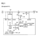
- FIG. 1 shows a conventional hot-swap circuit that uses a single MOSFET 100 (Q1) in series with a current sense resistor 102 (RS1) along with control circuitry for limiting current.
- a current limit amplifier 104 adjusts the MOSFET gate to source voltage in order to limit the voltage across the current sense resistor 102 and thus the current through the MOSFET 100.
- the current limit amplifier 104 compares a voltage representing the current in the current sense resistor 102 with a voltage VLIMIT produced by a voltage source 106 to control the gate of the MOSFET 100 so as to reduce the output current when the sensed current exceeds a maximum value established by the voltage VLIMIT.
- a current source 108 is provided for pulling up the gate voltage.
- a transistor 110 is provided for turning the hot swap circuit on or off.
- a timer circuit 112 sets a maximum time the MOSFET will operate in current limit.
- the timer circuit 112 is coupled to the status pin of the current limit amplifier 104 to detect the time moment when the current limit amplifier 104 begins limiting the current.
- the delay period set by the timer circuit 112 expires, the MOSFET 100 is turned off to protect it from overheating. The load will lose power and the hot swap controller will indicate that a fault has occurred.
- bypass capacitors 126 C L
- the load may be kept off until the bypass capacitors 126 are charged.
- a small charging current for the capacitance keeps the power in the MOSFET 100 low enough to prevent a dangerous rise in temperature.
- One method to reduce the charging current uses a capacitor 125 coupled between the MOSFET gate and ground to limit the voltage slew rate of the gate pin. The gate voltage is pulled up by a current from the current source 108 commonly in the range of 10-50 ⁇ A.
- the MOSFET 100 acts as a source follower while charging the load capacitance.
- Another method uses the current limit amplifier 104 to set the current charging the load capacitance.
- the hot-swap controller can provide an output indicating the power path is on (PATH_ON) to show that full current is available to the load.
- the on-state of a switch can be determined by monitoring its control signal. For the MOSFET switch 100, for example, this can be done with a hysteresis comparator 118 comparing the gate to source voltage of the MOSFET 100 with a threshold voltage produced by a voltage source 116 well above the MOSFET threshold voltage, for example, at 4.5 V.
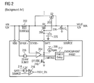
- the hot swap switch itself has resistance which is a source of power loss in the system. In MOSFET switches, this resistance is referred to as on-resistance. High power systems with large load currents have a significant power loss due to this on-resistance. Often, as illustrated in FIG. 2 , conventional high current hot-swap circuits use several MOSFETs 200, 203 (Q1 and Q2) arranged in parallel to achieve a low on-resistance that is unavailable using a single MOSFET.
- the hot swap circuit in FIG. 2 uses current and power control circuitry elements 202, 204, 206, 208 210, 212, 216, 218, 225, 226 similar to the respective elements in FIG. 1 .
- MOSFETs with both sufficient SOA capability and low enough on-resistance to serve as hot swap switches At high power levels it is difficult to find MOSFETs with both sufficient SOA capability and low enough on-resistance to serve as hot swap switches.
- High SOA capability is strongly linked to the amount of die area in a MOSFET that can dissipate the power. Most modern MOSFET production focuses on reducing both die area and on-resistance, which also reduces SOA capability. MOSFET processes with high SOA generally have high on-resistance per unit die area. Conversely, MOSFETS with low SOA tend to have low on-resistance per unit area. For high power applications, achieving the necessary SOA in a single MOSFET is often neither practical nor economical.
- Parallel MOSFETs share current well when their channels are fully enhanced because the MOSFET on-resistance has a positive temperature coefficient.
- parallel MOSFETs usually operate in saturation with high drain to source voltages. They do not share current well because their threshold voltages are not matched and have a negative temperature coefficient. This allows the MOSFET with the lowest threshold voltage to carry more current than the others. As this MOSFET heats it tends to carry even more current as its threshold voltage drops further. Thus, all of the load current may be carried by a single MOSFET. For this reason, when a group of parallel MOSFETs operate to limit current, they can only be relied on to have the SOA of a single MOSFET.
- a gate capacitor will limit inrush current to load capacitance. However, it does not limit current flowing to a resistive load or resistive fault across the load. This additional current adds to the stress imposed on the MOSFET switch and increases the required SOA.
- the present disclosure presents a novel system for supplying power from an input node to a load coupled to an output node.
- the system includes first and second switches coupled between the input node and the output node, a first limiting circuit configured for controlling the first switch so as to limit an output of first switch, and a second limiting circuit configured for controlling the second switch so as to limit an output of the second switch.
- the second limiting circuit is configured to operate independently of the first limiting circuit.
- the first limiting circuit may limit current though the first switch
- the second limiting circuit may limit current through the second switch.
- a logic circuit is provided to produce an output signal in response to first and second status signals.
- the first status signal indicates that the first limiting circuit is limiting the output of the first switch
- the second status signal indicates that the second current limit circuit is limiting the output of the second switch.
- the logic circuit produces an output signal after receiving both the first status signal and the second status signal.
- a timer circuit responsive to the output signal of the logic circuit may indicate a fault condition after expiration of a delay period.
- a first current sense element may be arranged for sensing the current in the first switch, and a second current sense element may be provided for sensing the current in the second switch.
- the first limiting circuit may be responsive to the current sensed by the first sense element, and the second limiting circuit may be responsive to the current sensed by the second sense element.
- the system may also have an indicative circuit for producing a path on signal indicating that a power path provided between the input node and the output node is turned on.
- the indicative circuit may include a first detecting circuit for detecting that the first switch is in an on state, and a second detecting circuit for detecting that the second switch is in an on state.
- the indicative circuit may be configured for producing the path on signal when either both the first and second switches are in an on state, or when one of the first and second switches is in an on state and a current limit circuit associated with the other of the first and second switches is in a current limit mode.
- the first switch may be coupled between the input node and the output node
- the second switch may be coupled in parallel to the first switch between the input node and the output node.
- the first and second switches may be turned on or off at the same time. Both the first and second switches may be turned off after expiration of the delay period.
- a system for supplying power from an input node to a load coupled to an output node may comprise first and second switches coupled between the input node and the output node, a first current limit circuit configured for controlling the first switch so as to limit current flowing through the first switch to a first value, and a second current limit circuit configured for controlling the second switch so as to limit a current flowing through the second switch to a second value greater than the first value.
- the second switch may be maintained in an off state when the first switch is turned on, and the second switch may be turned on in response to a signal indicating that the first switch is in an on state.
- the second switch may be configured to provide a low resistance path for a load current around the first switch.
- a first current sense element may be provided for sensing the current in the first switch, and a second current sense element may be provided for sensing the current in the second switch.
- the sensitivity of the first current sense element may be greater than the sensitivity of the second current sense element, where the current sense elements may be sense resistors and the sensitivity may correspond to electrical resistance of the respective resistors.
- the first current limit circuit may be responsive to the current sensed by the first sense element, and the second current limit circuit may be responsive to the current sensed by the second sense element.
- the system may further has a timer circuit including a first timer configured to initiate a first delay period in response to a first status signal indicating that the first current limit circuit begins operation in a current limit mode to limit the current through the first switch, and a second timer configured to initiate a second delay period in response to a second status signal indicating that the second current limit circuit begins operation in a current limit mode to limit the current through the second switch.
- the first delay period may be longer than the second delay period.
- the timer circuit may be configured to indicate a fault condition after expiration of the first delay period or the second delay period.
- the indicative circuit may be configured to produce the path on signal when the second switch is in an on state, without detecting the state of the first switch.
- a system for supplying power from an input node to a load coupled to an output node comprises first and second switches coupled between the input node and the output node, where the first switch is configured to dissipate more power than the second switch.
- a single limiting circuit may be configured for controlling the first switch so as to limit an output of the first switch, without regulating an output of the second switch.
- the single limiting circuit may be configured for controlling the first switch so as to limit current through the first switch when the second switch is turned off.
- the second switch may be maintained in an off state when the first switch is turned on, and the second switch may be turned on when the first switch is in an on state and a voltage across the second switch is below a threshold level.
- the second switch may be configured to provide a low resistance path for a load current around the first switch.
- the second switch may be turned off when a voltage across the second switch exceeds a threshold level, a gate to source voltage of the first switch falls below a threshold level, or the first switch is turned off.
- the indicative circuit may be configured to produce the path on signal when the first switch is in an on state, without detecting the state of the second switch.
- the present disclosure provides separate control circuits for controlling multiple MOSFETs. Such control allows multiple MOSFETs to be operated in parallel simultaneously or started up in stages with time delays between the stages. This allows the heating stress on the MOSFETs to be spread across multiple MOSFETs either simultaneously, or separated in time.
- separate control circuits for each switch can spread the power dissipation between the switches.
- the SOA capability of each switch is used more efficiently. Turning switches on at different times allows different MOSFETs to be used during startup inrush, input voltage step inrush, and when the load current is turned on. MOSFETs optimized for these different operating modes can be less expensive than MOSFETs required to handle all operating modes.
- the present disclosure will be made using specific examples of hot-swap controllers presented in FIGS. 3 , 4 and 5 . However, the disclosure is applicable to any switching circuits for supplying power to a load.
- FIG. 3 shows an exemplary embodiment of a hot-swap controller with two MOSFETs 300 and 302 simultaneously operating in parallel.
- Each MOSFET 300 and 302 is independently controlled using the respective current sense resistor 301 and 303, and the respective current limit amplifier 304 and 305.
- the current sense resistor 301 is coupled between positive node SENSE+1 and negative node SENSE-1 representing the MOSFET 300
- the current sense resistor 303 is coupled between positive node SENSE+2 and negative node SENSE-2 representing the MOSFET 302.
- Each of the current limit amplifiers 304 and 305 controls the gate of the respective MOSFET 300 and 302 independently from the other amplifier so as to limit current at the output of the MOSFETs 300 and 302 when the current sensed in the respective resistors 301 and 303 exceeds the maximum current value defined by the VLIMIT voltage provided by respective voltage sources 306 and 307.
- Current sources 308 and 309 provide current to pull up the gate voltage of the MOSFETs 300 and 302, respectively.
- Transistors 310 and 311 are provided for turning on and off the respective MOSFETs 300 and 302.
- Signals LIMITING 1 and LIMITING 2 respectively produced at status outputs of the current limit amplifiers 304 and 305 are supplied to respective inputs of an AND gate 313 that produces an output signal supplied to a timer 312 that sets a delay period for indicating an overcurrent fault condition.
- the independent gate control provided by the current limit amplifiers 304 and 305 divides the current and stress accurately between the MOSFETs 300 and 302 despite any mismatch in their threshold voltages or temperatures.
- the current limit amplifiers 304 and 305 can be used two smaller and less expensive MOSFETs. Board resistance, amplifier offset and mismatch effects can cause one of the current limit amplifiers 304 and 305 to limit current at a lower level than the second current limit amplifier. Since the MOSFET associated with the second current limit amplifier remains fully on, keeping drain to source voltage (VDS) low for both MOSFETs 300 and 302, neither MOSFET will suffer significant heating in this state. The combined impedance of the switches 300 and 302 is still low and the load may continue operating.
- VDS drain to source voltage
- the VDS and the dissipated power begin to increase, requiring the MOSFETS to be shut off for protection.
- the timer 312 is initiated only when both LIMITING 1 and LIMITING 2 signals are produced, i.e. when both of the current amplifiers 304 and 305 are operating to limit the current.
- an overcurrent fault signal is produced to indicate that both MOSFETs 300 and 302 should be turned OFF.
- the hot swap circuitry in FIG. 3 may include a circuit for producing a signal PATH_ON indicating that the power path is on, so as to show that full current is available to the load.
- This circuit includes threshold voltage sources 316, 317, hysteresis comparators 318, 319, AND gates 320, 321, 322 and an OR gate 323.
- the comparator 318 monitors when the gate to source voltage of the MOSFET 300 exceeds a threshold voltage produced by a voltage source 316, and the comparator 319 indicates when the gate to source voltage of the MOSFET 302 exceeds a threshold voltage produced by a voltage source 317. Both threshold voltages may be set well above the MOSFET threshold voltage, for example, at 4.5 V.
- One input of the AND gate 320 receives the output signal of the comparator 318, the other input of the AND gate 320 is supplied with the LIMITING 2 signal.
- the AND gate 321 is supplied with the output signals of the comparators 318 and 319.
- One input of the AND gate 322 receives the output signal of the comparator 319, whereas the other input of the AND gate 322 is supplied with the LIMITING 1 signal.
- the outputs of the AND gates 320, 321 and 322 are coupled to respective inputs of the OR gate 323.
- the OR gate 323 asserts the PATH_ON signal when either both MOSFETs are fully on, or if one of the MOSFETs is fully on while the other MOSFET operates in a current limit mode.
- the PATH_ON signal will be low if either of the MOSFETs 300 and 302 is turned off.
- FIG. 3 shows a bypass capacitor 326 provided at the load.
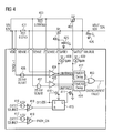
- the parallel MOSFETs can be operated in stages, as shown in FIG. 4 that presents an exemplary embodiment of a hot-swap controller with parallel MOSFETS 400 and 402.
- the MOSFET 400 may dissipate less power than the MOSFET 402.
- the MOSFET 400 operates as a startup MOSFET to bring up the load voltage and charge the load capacitance 426 while the load is held in a low current state. This allows the MOSFET 400 to have a high on-resistance, small current limit, and low SOA.
- the MOSFET 400 can be small and inexpensive.
- the MOSFET 402 operates as a shunt MOSFET which is turned on only after the startup MOSFET 400 is fully turned on.
- the hot swap controller in FIG. 4 includes current sense resistors 401 and 403 and the respective current limit amplifiers 404 and 305.
- the current sense resistor 401 is coupled between positive node SENSE+1 and negative node SENSE-1 to allow measurement of the current through the MOSFET 400
- the current sense resistor 403 is coupled between positive node SENSE+2 and negative node SENSE-2 to allow measurement of the current through the MOSFET 402.
- the current sense resistor 401 may have a much higher resistance that the resistance of the current sense resistor 403 so as to operate the MOSFET 400 at a smaller current limit than the MOSFET 402.
- the current limit amplifiers 404 and 405 control gates of the respective MOSFET 400 and 402 so as to limit current at the output of the MOSFETs 400 and 402 when the current sensed in the respective resistors 401 and 403 exceeds the maximum current value defined by the respective VLIMIT sources 406 and 407.
- Current sources 408 and 409 provide current to pull up the gate voltage of the MOSFETs 400 and 402, respectively.
- Transistors 410 and 411 are controlled for turning on and off the respective MOSFETs 400 and 402.
- the circuit in FIG. 4 may also include timers 412 and 414, an OR gate 413, an RS latch circuit 415, voltage sources 416 and 417, hysteresis comparators 418 and 419.
- a gate capacitor 425 may be coupled between the gate of the MOSFET 425 and ground to obtain the low charging current.
- a bypass load capacitor 426 may be coupled across the load.
- Signals LIMITING 1 and LIMITING 2 respectively produced at status outputs of the current limit amplifiers 404 and 405 are supplied to timers 412 and 414.
- a delay period defined by the timer 412 associated with the startup MOSFET 400 may be longer than the delay period of the timer 414 associated with the MOSFET 402.
- the shunt MOSFET 402 is turned on.
- the latch circuit 415 holds off the MOSFET 402 until the comparator 418 detects that the MOSFET 400 is on by determining that its gate to source voltage has exceeded a threshold voltage.
- the shunt MOSFET 402 provides a low resistance path for the load current around the MOSFET 400.
- the shunt MOSFET 402 is turned on when its VDS is small, it does not need a large SOA. It may also require a shorter delay period provided by the timer 414, corresponding to its smaller SOA. By applying power in stages with two MOSFETS 400 and 402, the SOA requirements of both MOSFETs are reduced and the on-resistance requirement of the MOSFET 400 can be larger.
- a PATH_ON signal indicating that the power path is on is produced by the comparator 419 when the gate to source voltage of the shunt MOSFET 402 has exceeded a threshold voltage, indicating that the low resistance channel is fully on and capable of supporting load current.
- the parallel MOSFETs in a hot-swap controller can be operated in stages as shown in FIG 5 that presents an exemplary embodiment of a hot-swap controller including MOSFETS 500 and 502, a single sense resistor 501 shared by both MOSFETs 500 and 502, and a single current limit amplifier 504 controlling the gate of the MOSFET 500 so as to limit its output current based on the voltage across the sense resistor 501 and the VLIMIT voltage produced by a voltage source 506.
- Current sources 508 and 509 provide current to pull up the gate voltage of the MOSFETs 500 and 502, respectively.
- Transistors 510 and 511 are controlled for turning on and off the respective MOSFETs 500 and 502.
- a timer 512 is coupled to the current limit amplifier 504 for detecting when it enters a current limit mode so as to assert an overcurrent fault condition signal after a delay period set by the timer 512 expires.
- the hot-swap controller in FIG. 5 also includes a hysteresis comparator 518 monitoring the gate to source voltage of the MOSFET 500 with respect to a threshold voltage produced by a voltage source 516.
- the output of the comparator 518 producing the PATH_ON signal is coupled to an inverter 520 that supplies a GATE1_OFF signal to an input of an OR gate 521.
- the output of the OR gate 521 produces a STRESS signal supplied to an input of an OR gate 522 that controls the gate of the transistor 511.
- the other input of the OR gate 522 is provided with an OFF/ON# signal that turns on and off the MOSFET 500.
- a hysteresis comparator 524 monitors the drain to source voltage of the MOSFETs 500 and 502 with respect to a threshold voltage produces by a voltage source 523, and supplies an output signal to an input of the OR gate 521 that produces the STRESS signal.
- the MOSFET 500 operates as a stress MOSFET to charge the load capacitance 526 and bring up the load voltage. It provides the load current during transients with limited durations such as startup and changes in input voltage.
- the MOSFET 500 has higher power dissipation than the MOSFET 502.
- the MOSFET 500 operates with both large current and large VDS, and has a high SOA rating.
- the MOSFET 500 does not require low on-resistance because it supports the load current only during limited duration transients. It may also require a long delay time provided by the timer 512.
- the MOSFET 502 operates as a shunt MOSFET to provide a low resistance path for the load current around the MOSFET 500 when conditions are stable and not changing.
- the MOSFET 502 is turned off by the signal STRESS to protect it whenever the VDS exceeds the threshold voltage provided by the voltage source 523 or if the gate to source voltage of the MOSFET 500 is below the threshold voltage provided by the voltage source 516, for example, when the MOSFET 500 operates in a current limit mode.
- the threshold voltage defined by the voltage source 523 may be set, for example, at 200 mV, and the threshold voltage of the voltage source 516 may be set, for example, at 4.5 V.
- the MOSFET 502 is only turned on when the STRESS signal is low, indicating that the MOSFET 500 is fully turned on and the VDS is below the threshold voltage defined by the voltage source 523. Therefore, the MOSFET 502 can have very low on-resistance. Because the MOSFET 502 is turned on with low VDS, it does not need a large SOA. The MOSFET 502 never operates in saturation, so several parallel MOSFETs may be used instead of the MOSFET 502 to achieve low on-resistance.
- the PATH_ON signal produced by the comparator 528 is derived from the on-state of the stress MOSFET 500. Whenever the MOSFET 500 is on, the load is allowed to draw power.
- the present disclosure makes it possible to improve SOA performance of a hot-swap controller using parallel MOSFETs that are separately controlled.
- Gate to source voltage levels of MOSFETs may be used as a condition to determine if a switch in the hot-swap controller is on.
- drain to source voltage levels of MOSFETs may be used as a condition to determine if a switch in the hot-swap controller is on.
- Combinations of switch on signals may be used for producing a PATH_ON signal to indicate if load current can be turned on.
- the configuration of the hot-swap controller can be extended to more parallel switch paths.
- FIGS. 3-5 a single MOSFET switch per path is shown in FIGS. 3-5 . However, each of these paths may use multiple MOSFET switches in parallel.
- N-type MOSFET switches are shown in the presented exemplary embodiments, the switches may be implemented with other devices, such as PMOS transistors, bipolar transistors, IGBTs or relays.
- the STRESS signal for the exemplary embodiment in FIG. 5 may be generated by monitoring the gate to source voltage, drain to source voltage, or detecting current limit in the STRESS MOSFET, or shunt MOSFET temperature, alone or in combination.
- the indication that a MOSFET is on can be derived by monitoring its gate to source voltage or its drain to source voltage, alone or in combination. Also, separate switch control circuits presented in FIGS. 3 , 4 and 5 may be used for controlling switches arranged in series, rather than in parallel, as shown in the exemplary embodiments.
Landscapes
- Engineering & Computer Science (AREA)
- Power Engineering (AREA)
- Electronic Switches (AREA)
- Emergency Protection Circuit Devices (AREA)
- Direct Current Feeding And Distribution (AREA)
- Supply And Distribution Of Alternating Current (AREA)
Abstract
Description
- This application claims priority of
US provisional patent application No 61/845,491 - This disclosure generally relates to circuits for limiting inrush currents and fault currents in electrical systems. In particular, the disclosure presents ways to operate multiple switches in parallel to limits inrush currents and fault currents in high power systems.
- A hot-swap circuit applies power from an input source to a load in a controlled and protected fashion. One function of such a controller is to limit inrush currents from the power source to the load, especially load capacitance, when power is first applied or if the power source voltage suddenly increases. Another function is to limit current if the load attempts to draw too much current, for example if there is a short circuit in the load.
-
FIG. 1 shows a conventional hot-swap circuit that uses a single MOSFET 100 (Q1) in series with a current sense resistor 102 (RS1) along with control circuitry for limiting current. Numerous such circuits are commercially available. When limiting current, acurrent limit amplifier 104 adjusts the MOSFET gate to source voltage in order to limit the voltage across thecurrent sense resistor 102 and thus the current through theMOSFET 100. Thecurrent limit amplifier 104 compares a voltage representing the current in thecurrent sense resistor 102 with a voltage VLIMIT produced by avoltage source 106 to control the gate of theMOSFET 100 so as to reduce the output current when the sensed current exceeds a maximum value established by the voltage VLIMIT. Acurrent source 108 is provided for pulling up the gate voltage. Atransistor 110 is provided for turning the hot swap circuit on or off. - During this time, the voltage and current through the
MOSFET 100 can both be large, resulting in high power dissipation in theMOSFET 100. If this power dissipation persists, theMOSFET 100 can reach temperatures that cause damage. MOSFET manufacturers present the safe limits on MOSFET voltage, current and time, as a curve referred to as Safe Operating Area (SOA). Commonly, atimer circuit 112 sets a maximum time the MOSFET will operate in current limit. Thetimer circuit 112 is coupled to the status pin of thecurrent limit amplifier 104 to detect the time moment when thecurrent limit amplifier 104 begins limiting the current. When the delay period set by thetimer circuit 112 expires, theMOSFET 100 is turned off to protect it from overheating. The load will lose power and the hot swap controller will indicate that a fault has occurred. - Often high power hot-swap applications need to charge large bypass capacitors 126 (CL) across the load. To reduce stress on the
MOSFET 100, the load may be kept off until thebypass capacitors 126 are charged. A small charging current for the capacitance keeps the power in theMOSFET 100 low enough to prevent a dangerous rise in temperature. One method to reduce the charging current uses acapacitor 125 coupled between the MOSFET gate and ground to limit the voltage slew rate of the gate pin. The gate voltage is pulled up by a current from thecurrent source 108 commonly in the range of 10-50µA. TheMOSFET 100 acts as a source follower while charging the load capacitance. Another method uses thecurrent limit amplifier 104 to set the current charging the load capacitance. Either method can lower the inrush current such that the startup period stays within the SOA of theMOSFET 100. When the charging is finished, the hot-swap controller can provide an output indicating the power path is on (PATH_ON) to show that full current is available to the load. The on-state of a switch can be determined by monitoring its control signal. For theMOSFET switch 100, for example, this can be done with ahysteresis comparator 118 comparing the gate to source voltage of theMOSFET 100 with a threshold voltage produced by avoltage source 116 well above the MOSFET threshold voltage, for example, at 4.5 V. - The hot swap switch itself has resistance which is a source of power loss in the system. In MOSFET switches, this resistance is referred to as on-resistance. High power systems with large load currents have a significant power loss due to this on-resistance. Often, as illustrated in
FIG. 2 , conventional high current hot-swap circuits use several MOSFETs 200, 203 (Q1 and Q2) arranged in parallel to achieve a low on-resistance that is unavailable using a single MOSFET. The hot swap circuit inFIG. 2 uses current and powercontrol circuitry elements FIG. 1 . - At high power levels it is difficult to find MOSFETs with both sufficient SOA capability and low enough on-resistance to serve as hot swap switches. High SOA capability is strongly linked to the amount of die area in a MOSFET that can dissipate the power. Most modern MOSFET production focuses on reducing both die area and on-resistance, which also reduces SOA capability. MOSFET processes with high SOA generally have high on-resistance per unit die area. Conversely, MOSFETS with low SOA tend to have low on-resistance per unit area. For high power applications, achieving the necessary SOA in a single MOSFET is often neither practical nor economical.
- Using multiple MOSFETs in parallel reduces the combined on-resistance, but does not necessarily increase the SOA. Parallel MOSFETs share current well when their channels are fully enhanced because the MOSFET on-resistance has a positive temperature coefficient. However, when limiting current parallel MOSFETs usually operate in saturation with high drain to source voltages. They do not share current well because their threshold voltages are not matched and have a negative temperature coefficient. This allows the MOSFET with the lowest threshold voltage to carry more current than the others. As this MOSFET heats it tends to carry even more current as its threshold voltage drops further. Thus, all of the load current may be carried by a single MOSFET. For this reason, when a group of parallel MOSFETs operate to limit current, they can only be relied on to have the SOA of a single MOSFET.
- Not all loads can be turned off during startup and inrush. A gate capacitor will limit inrush current to load capacitance. However, it does not limit current flowing to a resistive load or resistive fault across the load. This additional current adds to the stress imposed on the MOSFET switch and increases the required SOA.
- Therefore, it would be desirable to develop inrush current control circuitry and methodology for controlling multiple switches so as to overcome the above discussed disadvantages.
- The present disclosure presents a novel system for supplying power from an input node to a load coupled to an output node.
- In accordance with one aspect of the disclosure the system includes first and second switches coupled between the input node and the output node, a first limiting circuit configured for controlling the first switch so as to limit an output of first switch, and a second limiting circuit configured for controlling the second switch so as to limit an output of the second switch. The second limiting circuit is configured to operate independently of the first limiting circuit. For example, the first limiting circuit may limit current though the first switch, and the second limiting circuit may limit current through the second switch. A logic circuit is provided to produce an output signal in response to first and second status signals. The first status signal indicates that the first limiting circuit is limiting the output of the first switch, and the second status signal indicates that the second current limit circuit is limiting the output of the second switch. The logic circuit produces an output signal after receiving both the first status signal and the second status signal.
- A timer circuit responsive to the output signal of the logic circuit may indicate a fault condition after expiration of a delay period.
- A first current sense element may be arranged for sensing the current in the first switch, and a second current sense element may be provided for sensing the current in the second switch.
- The first limiting circuit may be responsive to the current sensed by the first sense element, and the second limiting circuit may be responsive to the current sensed by the second sense element.
- The system may also have an indicative circuit for producing a path on signal indicating that a power path provided between the input node and the output node is turned on. The indicative circuit may include a first detecting circuit for detecting that the first switch is in an on state, and a second detecting circuit for detecting that the second switch is in an on state.
- The indicative circuit may be configured for producing the path on signal when either both the first and second switches are in an on state, or when one of the first and second switches is in an on state and a current limit circuit associated with the other of the first and second switches is in a current limit mode.
- In an exemplary embodiment, the first switch may be coupled between the input node and the output node, and the second switch may be coupled in parallel to the first switch between the input node and the output node. The first and second switches may be turned on or off at the same time. Both the first and second switches may be turned off after expiration of the delay period.
- In accordance with another aspect of the disclosure, a system for supplying power from an input node to a load coupled to an output node may comprise first and second switches coupled between the input node and the output node, a first current limit circuit configured for controlling the first switch so as to limit current flowing through the first switch to a first value, and a second current limit circuit configured for controlling the second switch so as to limit a current flowing through the second switch to a second value greater than the first value.
- The second switch may be maintained in an off state when the first switch is turned on, and the second switch may be turned on in response to a signal indicating that the first switch is in an on state. The second switch may be configured to provide a low resistance path for a load current around the first switch.
- A first current sense element may be provided for sensing the current in the first switch, and a second current sense element may be provided for sensing the current in the second switch. The sensitivity of the first current sense element may be greater than the sensitivity of the second current sense element, where the current sense elements may be sense resistors and the sensitivity may correspond to electrical resistance of the respective resistors. The first current limit circuit may be responsive to the current sensed by the first sense element, and the second current limit circuit may be responsive to the current sensed by the second sense element.
- The system may further has a timer circuit including a first timer configured to initiate a first delay period in response to a first status signal indicating that the first current limit circuit begins operation in a current limit mode to limit the current through the first switch, and a second timer configured to initiate a second delay period in response to a second status signal indicating that the second current limit circuit begins operation in a current limit mode to limit the current through the second switch. The first delay period may be longer than the second delay period. The timer circuit may be configured to indicate a fault condition after expiration of the first delay period or the second delay period.
- The indicative circuit may be configured to produce the path on signal when the second switch is in an on state, without detecting the state of the first switch.
- In accordance with a further aspect of the disclosure, a system for supplying power from an input node to a load coupled to an output node comprises first and second switches coupled between the input node and the output node, where the first switch is configured to dissipate more power than the second switch. A single limiting circuit may be configured for controlling the first switch so as to limit an output of the first switch, without regulating an output of the second switch. For example, the single limiting circuit may be configured for controlling the first switch so as to limit current through the first switch when the second switch is turned off.
- The second switch may be maintained in an off state when the first switch is turned on, and the second switch may be turned on when the first switch is in an on state and a voltage across the second switch is below a threshold level. The second switch may be configured to provide a low resistance path for a load current around the first switch. The second switch may be turned off when a voltage across the second switch exceeds a threshold level, a gate to source voltage of the first switch falls below a threshold level, or the first switch is turned off.
- The indicative circuit may be configured to produce the path on signal when the first switch is in an on state, without detecting the state of the second switch.
- Additional advantages and aspects of the disclosure will become readily apparent to those skilled in the art from the following detailed description, wherein embodiments of the present disclosure are shown and described, simply by way of illustration of the best mode contemplated for practicing the present disclosure. As will be described, the disclosure is capable of other and different embodiments, and its several details are susceptible of modification in various obvious respects, all without departing from the spirit of the disclosure. Accordingly, the drawings and description are to be regarded as illustrative in nature, and not as limitative.
- The following detailed description of the embodiments of the present disclosure can best be understood when read in conjunction with the following drawings, in which the features are not necessarily drawn to scale but rather are drawn as to best illustrate the pertinent features, wherein:
-
Figs. 1 and2 illustrate conventional hot swap controllers. -
Fig. 3 illustrates a first exemplary embodiment of a hot swap controller in accordance with the present disclosure. -
Fig. 4 illustrates a second exemplary embodiment of a hot swap controller in accordance with the present disclosure. -
Fig. 5 illustrates a third exemplary embodiment of a hot swap controller in accordance with the present disclosure. - The present disclosure provides separate control circuits for controlling multiple MOSFETs. Such control allows multiple MOSFETs to be operated in parallel simultaneously or started up in stages with time delays between the stages. This allows the heating stress on the MOSFETs to be spread across multiple MOSFETs either simultaneously, or separated in time.
- In accordance with the present disclosure, separate control circuits for each switch can spread the power dissipation between the switches. The SOA capability of each switch is used more efficiently. Turning switches on at different times allows different MOSFETs to be used during startup inrush, input voltage step inrush, and when the load current is turned on. MOSFETs optimized for these different operating modes can be less expensive than MOSFETs required to handle all operating modes.
- The present disclosure will be made using specific examples of hot-swap controllers presented in
FIGS. 3 ,4 and5 . However, the disclosure is applicable to any switching circuits for supplying power to a load. -
FIG. 3 shows an exemplary embodiment of a hot-swap controller with twoMOSFETs MOSFET current sense resistor current limit amplifier current sense resistor 301 is coupled between positive node SENSE+1 and negative node SENSE-1 representing theMOSFET 300, and thecurrent sense resistor 303 is coupled between positive node SENSE+2 and negative node SENSE-2 representing theMOSFET 302. Each of thecurrent limit amplifiers respective MOSFET MOSFETs respective resistors respective voltage sources Current sources MOSFETs Transistors respective MOSFETs - Signals LIMITING 1 and LIMITING 2 respectively produced at status outputs of the
current limit amplifiers gate 313 that produces an output signal supplied to atimer 312 that sets a delay period for indicating an overcurrent fault condition. - When limiting current, the independent gate control provided by the
current limit amplifiers MOSFETs current limit amplifiers MOSFETs switches - Only when the load current increases to a point where both
MOSFETs gate 313, thetimer 312 is initiated only when both LIMITING 1 and LIMITING 2 signals are produced, i.e. when both of thecurrent amplifiers timer 312 expires, an overcurrent fault signal is produced to indicate that bothMOSFETs - Further, the hot swap circuitry in
FIG. 3 may include a circuit for producing a signal PATH_ON indicating that the power path is on, so as to show that full current is available to the load. This circuit includesthreshold voltage sources hysteresis comparators gates OR gate 323. Thecomparator 318 monitors when the gate to source voltage of theMOSFET 300 exceeds a threshold voltage produced by avoltage source 316, and thecomparator 319 indicates when the gate to source voltage of theMOSFET 302 exceeds a threshold voltage produced by avoltage source 317. Both threshold voltages may be set well above the MOSFET threshold voltage, for example, at 4.5 V. - One input of the AND
gate 320 receives the output signal of thecomparator 318, the other input of the ANDgate 320 is supplied with the LIMITING 2 signal. The ANDgate 321 is supplied with the output signals of thecomparators gate 322 receives the output signal of thecomparator 319, whereas the other input of the ANDgate 322 is supplied with the LIMITING 1 signal. The outputs of the ANDgates OR gate 323. As a result, theOR gate 323 asserts the PATH_ON signal when either both MOSFETs are fully on, or if one of the MOSFETs is fully on while the other MOSFET operates in a current limit mode. The PATH_ON signal will be low if either of theMOSFETs FIG. 3 shows abypass capacitor 326 provided at the load. - In applications where inrush current can be limited to low levels, the parallel MOSFETs can be operated in stages, as shown in
FIG. 4 that presents an exemplary embodiment of a hot-swap controller withparallel MOSFETS MOSFET 400 may dissipate less power than theMOSFET 402. In particular, theMOSFET 400 operates as a startup MOSFET to bring up the load voltage and charge theload capacitance 426 while the load is held in a low current state. This allows theMOSFET 400 to have a high on-resistance, small current limit, and low SOA. Thus, theMOSFET 400 can be small and inexpensive. As discussed below, theMOSFET 402 operates as a shunt MOSFET which is turned on only after thestartup MOSFET 400 is fully turned on. - The hot swap controller in
FIG. 4 includescurrent sense resistors current limit amplifiers current sense resistor 401 is coupled between positive node SENSE+1 and negative node SENSE-1 to allow measurement of the current through theMOSFET 400, and thecurrent sense resistor 403 is coupled between positive node SENSE+2 and negative node SENSE-2 to allow measurement of the current through theMOSFET 402. Thecurrent sense resistor 401 may have a much higher resistance that the resistance of thecurrent sense resistor 403 so as to operate theMOSFET 400 at a smaller current limit than theMOSFET 402. - The
current limit amplifiers respective MOSFET MOSFETs respective resistors respective VLIMIT sources Current sources MOSFETs Transistors respective MOSFETs - The circuit in
FIG. 4 may also includetimers gate 413, anRS latch circuit 415,voltage sources hysteresis comparators gate capacitor 425 may be coupled between the gate of theMOSFET 425 and ground to obtain the low charging current. Abypass load capacitor 426 may be coupled across the load. - Signals LIMITING 1 and LIMITING 2 respectively produced at status outputs of the
current limit amplifiers timers timer 412 associated with thestartup MOSFET 400 may be longer than the delay period of thetimer 414 associated with theMOSFET 402. - After the
startup MOSFET 400 has turned on completely, theshunt MOSFET 402 is turned on. Thelatch circuit 415 holds off theMOSFET 402 until thecomparator 418 detects that theMOSFET 400 is on by determining that its gate to source voltage has exceeded a threshold voltage. Theshunt MOSFET 402 provides a low resistance path for the load current around theMOSFET 400. - Because the
shunt MOSFET 402 is turned on when its VDS is small, it does not need a large SOA. It may also require a shorter delay period provided by thetimer 414, corresponding to its smaller SOA. By applying power in stages with twoMOSFETS MOSFET 400 can be larger. A PATH_ON signal indicating that the power path is on is produced by thecomparator 419 when the gate to source voltage of theshunt MOSFET 402 has exceeded a threshold voltage, indicating that the low resistance channel is fully on and capable of supporting load current. - Some applications have loads that are always on, even during startup, or are subject to input steps and output surges that put additional stress on the hot-swap MOSFET. In such cases, the parallel MOSFETs in a hot-swap controller can be operated in stages as shown in
FIG 5 that presents an exemplary embodiment of a hot-swapcontroller including MOSFETS single sense resistor 501 shared by bothMOSFETs current limit amplifier 504 controlling the gate of theMOSFET 500 so as to limit its output current based on the voltage across thesense resistor 501 and the VLIMIT voltage produced by avoltage source 506.Current sources MOSFETs Transistors respective MOSFETs timer 512 is coupled to thecurrent limit amplifier 504 for detecting when it enters a current limit mode so as to assert an overcurrent fault condition signal after a delay period set by thetimer 512 expires. - The hot-swap controller in
FIG. 5 also includes ahysteresis comparator 518 monitoring the gate to source voltage of theMOSFET 500 with respect to a threshold voltage produced by avoltage source 516. The output of thecomparator 518 producing the PATH_ON signal is coupled to aninverter 520 that supplies a GATE1_OFF signal to an input of anOR gate 521. The output of theOR gate 521 produces a STRESS signal supplied to an input of anOR gate 522 that controls the gate of thetransistor 511. The other input of theOR gate 522 is provided with an OFF/ON# signal that turns on and off theMOSFET 500. Ahysteresis comparator 524 monitors the drain to source voltage of theMOSFETs voltage source 523, and supplies an output signal to an input of theOR gate 521 that produces the STRESS signal. - The
MOSFET 500 operates as a stress MOSFET to charge theload capacitance 526 and bring up the load voltage. It provides the load current during transients with limited durations such as startup and changes in input voltage. TheMOSFET 500 has higher power dissipation than theMOSFET 502. TheMOSFET 500 operates with both large current and large VDS, and has a high SOA rating. However, theMOSFET 500 does not require low on-resistance because it supports the load current only during limited duration transients. It may also require a long delay time provided by thetimer 512. - The
MOSFET 502 operates as a shunt MOSFET to provide a low resistance path for the load current around theMOSFET 500 when conditions are stable and not changing. TheMOSFET 502 is turned off by the signal STRESS to protect it whenever the VDS exceeds the threshold voltage provided by thevoltage source 523 or if the gate to source voltage of theMOSFET 500 is below the threshold voltage provided by thevoltage source 516, for example, when theMOSFET 500 operates in a current limit mode. The threshold voltage defined by thevoltage source 523 may be set, for example, at 200 mV, and the threshold voltage of thevoltage source 516 may be set, for example, at 4.5 V. - The
MOSFET 502 is only turned on when the STRESS signal is low, indicating that theMOSFET 500 is fully turned on and the VDS is below the threshold voltage defined by thevoltage source 523. Therefore, theMOSFET 502 can have very low on-resistance. Because theMOSFET 502 is turned on with low VDS, it does not need a large SOA. TheMOSFET 502 never operates in saturation, so several parallel MOSFETs may be used instead of theMOSFET 502 to achieve low on-resistance. The PATH_ON signal produced by the comparator 528 is derived from the on-state of thestress MOSFET 500. Whenever theMOSFET 500 is on, the load is allowed to draw power. - Hence, the present disclosure makes it possible to improve SOA performance of a hot-swap controller using parallel MOSFETs that are separately controlled.
- Gate to source voltage levels of MOSFETs may be used as a condition to determine if a switch in the hot-swap controller is on. Alternatively, drain to source voltage levels of MOSFETs may be used as a condition to determine if a switch in the hot-swap controller is on. Combinations of switch on signals may be used for producing a PATH_ON signal to indicate if load current can be turned on.
- Although two switch paths are shown in exemplary embodiments in
FIGS. 3-5 , the configuration of the hot-swap controller can be extended to more parallel switch paths. - Also, a single MOSFET switch per path is shown in
FIGS. 3-5 . However, each of these paths may use multiple MOSFET switches in parallel. - In addition, although N-type MOSFET switches are shown in the presented exemplary embodiments, the switches may be implemented with other devices, such as PMOS transistors, bipolar transistors, IGBTs or relays.
- Further, the STRESS signal for the exemplary embodiment in
FIG. 5 may be generated by monitoring the gate to source voltage, drain to source voltage, or detecting current limit in the STRESS MOSFET, or shunt MOSFET temperature, alone or in combination. - The indication that a MOSFET is on can be derived by monitoring its gate to source voltage or its drain to source voltage, alone or in combination. Also, separate switch control circuits presented in
FIGS. 3 ,4 and5 may be used for controlling switches arranged in series, rather than in parallel, as shown in the exemplary embodiments. - The foregoing description illustrates and describes aspects of the present invention. Additionally, the disclosure shows and describes only preferred embodiments, but as aforementioned, it is to be understood that the invention is capable of use in various other combinations, modifications, and environments and is capable of changes or modifications within the scope of the inventive concept as expressed herein, commensurate with the above teachings, and/or the skill or knowledge of the relevant art.
- The embodiments described hereinabove are further intended to explain best modes known of practicing the invention and to enable others skilled in the art to utilize the invention in such, or other, embodiments and with the various modifications required by the particular applications or uses of the invention. Accordingly, the description is not intended to limit the invention to the form disclosed herein.
Claims (15)
- A system for supplying power from an input node to a load coupled to an output node, comprising:first and second switches coupled between the input node and the output node, a first limiting circuit configured for controlling the first switch so as to limit an output of the first switch,a second limiting circuit configured for controlling the second switch so as to limit an output of the second switch, the second limiting circuit being configured to operate independently of the first limiting circuit, anda logic circuit responsive to a first status signal indicating that the first limiting circuit is limiting the output of the first switch, and responsive to a second status signal indicating that the second current limit circuit is limiting the output of the second switch,the logic circuit being configured to produce an output signal after receiving both the first status signal and the second status signal.
- The system of claim 1,
wherein the first limiting circuit limits current through the first switch, and the second limiting circuit limits current through the second switch, or
wherein the first switch is coupled between the input node and the output node, and the second switch is coupled in parallel to the first switch between the input node and the output node, or
wherein the first and second switches are turned on or off at the same time. - The system of claim 1 or 2 further comprising a timer circuit responsive to the output signal of the logic circuit for indicating a fault condition after expiration of a delay period.
- The system of claim 3, wherein both the first and second switches are turned off after expiration of the delay period.
- The system of any one of the preceding claims, further comprising a first current sense element for sensing the current in the first switch, and a second current sense element for sensing the current in the second switch, wherein the first limiting circuit is responsive to the current sensed by the first sense element, and the second limiting circuit is responsive to the current sensed by the second sense element.
- The system of any one of the preceding claims, further comprising an indicative circuit for producing a path on signal indicating that a power path provided between the input node and the output node is turned on, the indicative circuit including:a first detecting circuit for detecting that the first switch is in an on state, anda second detecting circuit for detecting that the second switch is in an on state,wherein the indicative circuit is configured for producing the path on signal when either both the first and second switches are in an on state, or when one of the first and second switches is in an on state and a limiting circuit associated with the other of the first and second switches is limiting an output of the respective switch.
- A system for supplying power from an input node to a load coupled to an output node, comprising:first and second switches coupled between the input node and the output node,a first current limit circuit configured for controlling the first switch so as to limit current flowing through the first switch to a first value, anda second current limit circuit configured for controlling the second switch so as to limit a current flowing through the second switch to a second value greater than the first value.
- The system of claim 7,
wherein the second switch is maintained in an off state when the first switch is turned on, and the second switch is turned on in response to a signal indicating that the first switch is in an on state, or
wherein the second switch is configured to provide a low resistance path for a load current around the first switch. - The system of claim 7 or 8, further comprising a first current sense element for sensing the current in the first switch, and a second current sense element for sensing the current in the second switch, wherein sensitivity of the first current sense element is greater than sensitivity of the second current sense element, wherein the first current limit circuit is responsive to the current sensed by the first sense element, and the second current limit circuit is responsive to the current sensed by the second sense element.
- The system of any one of claims 7 to 9, further comprising a timer circuit including:a first timer configured to initiate a first delay period in response to a first status signal indicating that the first current limit circuit begins operation in a current limit mode to limit the current through the first switch, anda second timer configured to initiate a second delay period in response to a second status signal indicating that the second current limit circuit begins operation in a current limit mode to limit the current through the second switch,wherein the timer circuit is configured to indicate a fault condition after expiration of the first delay period or the second delay period.
- The system of any one of claims 7 to 10, further comprising an indicative circuit for producing a path on signal indicating that a power path provided between the input node and the output node is turned on, the indicative circuit is configured to produce the path on signal when the second switch is in an on state, without detecting the state of the first switch.
- A system for supplying power from an input node to a load coupled to an output node, comprising:first and second switches coupled between the input node and the output node, the first switch is configured to dissipate more power than the second switch, anda limiting circuit configured for controlling the first switch so as to limit output of the first switch, without regulating an output of the second switch.
- The system of claim 12,
wherein the limiting circuit limits current through the first switch, and/or
wherein the limiting circuit is configured for controlling the first switch so as to limit current flowing through the first switch when the second switch is turned off. - The system of claim 12 or 13,
wherein the second switch is maintained in an off state when the first switch is turned on, and the second switch is turned on when the first switch is in an on state and a voltage across the second switch is below a threshold level, or
wherein the second switch is configured to provide a low resistance path for a load current around the first switch, or
wherein the second switch is turned off when a voltage across the second switch exceeds a threshold level, or
wherein the second switch is turned off when a gate to source voltage of the first switch falls below a threshold level, or
wherein the second switch is turned off when the first switch is turned off. - The system of any one of claims 12 to 14, further comprising an indicative circuit for producing a path on signal indicating that a power path provided between the input node and the output node is turned on, the indicative circuit is configured to produce the path on signal when the first switch is in an on state, without detecting the state of the second switch.
Applications Claiming Priority (2)
| Application Number | Priority Date | Filing Date | Title |
|---|---|---|---|
| US201361845491P | 2013-07-12 | 2013-07-12 | |
| US14/300,999 US10003190B2 (en) | 2013-07-12 | 2014-06-10 | Inrush control with multiple switches |
Publications (2)
| Publication Number | Publication Date |
|---|---|
| EP2852018A2 true EP2852018A2 (en) | 2015-03-25 |
| EP2852018A3 EP2852018A3 (en) | 2015-07-22 |
Family
ID=52276898
Family Applications (1)
| Application Number | Title | Priority Date | Filing Date |
|---|---|---|---|
| EP14002344.1A Withdrawn EP2852018A3 (en) | 2013-07-12 | 2014-07-08 | Inrush control with multiple switches |
Country Status (5)
| Country | Link |
|---|---|
| US (2) | US10003190B2 (en) |
| EP (1) | EP2852018A3 (en) |
| JP (1) | JP6632794B2 (en) |
| KR (1) | KR102306521B1 (en) |
| TW (2) | TWI718397B (en) |
Cited By (2)
| Publication number | Priority date | Publication date | Assignee | Title |
|---|---|---|---|---|
| US10418805B2 (en) | 2013-07-12 | 2019-09-17 | Linear Technology Llc | Inrush control with multiple switches |
| EP3784757A4 (en) * | 2018-04-23 | 2021-12-22 | Asphalt Sciences, LLC | System and method for generating tire rubber asphalt |
Families Citing this family (21)
| Publication number | Priority date | Publication date | Assignee | Title |
|---|---|---|---|---|
| US9671465B2 (en) | 2013-07-12 | 2017-06-06 | Linear Technology Corporation | Detecting faults in hot-swap applications |
| JP6402591B2 (en) * | 2014-10-31 | 2018-10-10 | 富士電機株式会社 | Semiconductor device |
| US9917437B2 (en) * | 2015-05-06 | 2018-03-13 | Cisco Technology, Inc. | Hot swap controller with individually controlled parallel current paths |
| DE102015114460B4 (en) * | 2015-08-31 | 2022-06-09 | Infineon Technologies Ag | Supply load with inrush current behavior |
| US10418986B2 (en) * | 2015-12-14 | 2019-09-17 | Monolithic Power Systems, Inc. | Monolithic integrated circuit switch device with output current balancing for parallel-connection |
| US10283970B2 (en) | 2016-07-11 | 2019-05-07 | Analog Devices, Inc. | Dynamic exchange of electrical current control devices in a load current controller |
| IT201600088220A1 (en) * | 2016-08-30 | 2018-03-02 | St Microelectronics Srl | CIRCUIT OF ELECTRONIC FUSE, EQUIPMENT AND CORRESPONDENT PROCEDURE |
| IT201600123267A1 (en) * | 2016-12-05 | 2018-06-05 | St Microelectronics Srl | CURRENT LIMITER, EQUIPMENT AND CORRESPONDENT PROCEDURE |
| US10381822B2 (en) * | 2016-12-12 | 2019-08-13 | Google Llc | Oring control using low voltage device for high voltage DC rack |
| US10498131B2 (en) * | 2016-12-30 | 2019-12-03 | Infineon Technologies Ag | Electronic switch and protection circuit |
| US11013929B2 (en) | 2017-02-28 | 2021-05-25 | Medtronic, Inc. | Power management for an implantable device |
| US10630070B2 (en) * | 2017-04-18 | 2020-04-21 | Alexander Faingersh | Device and method for overcurrent protection |
| EP3844376A4 (en) * | 2018-08-30 | 2022-06-08 | Watt Fuel Cell Corp. | Safety control system and method for fuel-consuming apparatus |
| US11251607B2 (en) * | 2018-12-06 | 2022-02-15 | Hewlett Packard Enterprise Development Lp | Fuse having parallel transorb device with switch |
| US11594870B2 (en) * | 2019-04-18 | 2023-02-28 | Dell Products L.P. | Systems and methods for extending fault timer to prevent overcurrent protection shutdown during powering on of information handling system |
| JP7368132B2 (en) * | 2019-07-22 | 2023-10-24 | ローム株式会社 | series regulator |
| US11474581B2 (en) * | 2019-08-09 | 2022-10-18 | Analog Devices International Unlimited Company | Communication terminal for hot-swap controllers |
| EP3787139A1 (en) | 2019-08-29 | 2021-03-03 | Aptiv Technologies Limited | Electrical safety system for providing overcurrent protection of an electrical circuit in a vehicle |
| US11316509B1 (en) * | 2020-06-19 | 2022-04-26 | ZT Group Int'l, Inc. | Maintaining safe operating area operation of transistors during ramp up |
| US11418022B2 (en) | 2020-07-29 | 2022-08-16 | Sl Power Electronics Corporation | Active inrush current limiter |
| US11870428B1 (en) * | 2022-08-26 | 2024-01-09 | Infineon Technologies Austria Ag | System and method for pulsed gate control of a transistor |
Family Cites Families (29)
| Publication number | Priority date | Publication date | Assignee | Title |
|---|---|---|---|---|
| GB395700A (en) * | 1932-01-18 | 1933-07-18 | Stanley Herbert Attwood | Improvements relating to valve operating mechanism for internal combustion engines |
| JPH05168142A (en) * | 1991-12-12 | 1993-07-02 | Hitachi Ltd | Ground fault detector and detection protector at different points on distribution line |
| US5428287A (en) * | 1992-06-16 | 1995-06-27 | Cherry Semiconductor Corporation | Thermally matched current limit circuit |
| US5428267A (en) | 1992-07-09 | 1995-06-27 | Premier Power Systems, Inc. | Regulated DC power supply |
| JPH07121252A (en) * | 1993-10-26 | 1995-05-12 | Rohm Co Ltd | Ic incorporating stabilized power circuit |
| JPH0897710A (en) * | 1994-09-28 | 1996-04-12 | Hitachi Ltd | Programmable two-wire two-phase system logic array |
| JPH1041797A (en) * | 1996-05-21 | 1998-02-13 | Harness Sogo Gijutsu Kenkyusho:Kk | Switch circuit with excess current detecting function |
| US5698973A (en) | 1996-07-31 | 1997-12-16 | Data General Corporation | Soft-start switch with voltage regulation and current limiting |
| US6798175B2 (en) | 2000-04-11 | 2004-09-28 | Pentax Corporation | Power supply circuit |
| JP2001298861A (en) * | 2000-04-11 | 2001-10-26 | Asahi Optical Co Ltd | Power source circuit and electronic still camera |
| US6704183B2 (en) * | 2001-03-27 | 2004-03-09 | Agilent Technologies, Inc. | Fault detection in a LED bias circuit |
| CN100372202C (en) * | 2002-01-08 | 2008-02-27 | 台达电子工业股份有限公司 | Circuit for restraining surge current |
| JP2004185406A (en) * | 2002-12-04 | 2004-07-02 | Fujitsu Ten Ltd | Excess current protecting apparatus |
| US7962931B2 (en) | 2002-12-23 | 2011-06-14 | Coupons.Com Incorporated | Method and system for integrating television brand advertising with promotional marketing |
| JP4405327B2 (en) * | 2004-06-30 | 2010-01-27 | 本田技研工業株式会社 | Front fender structure |
| JP2006053898A (en) * | 2004-07-15 | 2006-02-23 | Rohm Co Ltd | Overcurrent protection circuit and voltage generation circuit and electronic equipment using it |
| JP2006148886A (en) | 2004-10-27 | 2006-06-08 | Stmicroelectronics Sa | Protection of power transistor |
| US7035071B1 (en) * | 2004-12-29 | 2006-04-25 | Texas Instruments Incorporated | Current limit with adaptive cycle skipping for switching regulators |
| US20080043393A1 (en) * | 2006-08-18 | 2008-02-21 | Honeywell International Inc. | Power switching device |
| US7957116B2 (en) * | 2006-10-13 | 2011-06-07 | Advanced Analogic Technologies, Inc. | System and method for detection of multiple current limits |
| US7821753B2 (en) | 2007-01-18 | 2010-10-26 | Alcatel-Lucent Usa Inc. | DC high power distribution assembly |
| CN101217252B (en) | 2008-01-04 | 2010-09-01 | 华中科技大学 | A soft start circuit for PDM DC-DC switching power supply |
| CN101217262A (en) | 2008-01-21 | 2008-07-09 | 四川虹微技术有限公司 | A class D power amplifier and the corresponding input signal modulation method |
| JP4479800B2 (en) * | 2008-01-28 | 2010-06-09 | 株式会社デンソー | Switching power supply |
| US7760479B2 (en) | 2008-04-09 | 2010-07-20 | Fairchild Semiconductor Corporation | Technique for combining in-rush current limiting and short circuit current limiting |
| JP5431994B2 (en) * | 2010-02-10 | 2014-03-05 | ルネサスエレクトロニクス株式会社 | Current limit circuit |
| US8680893B2 (en) * | 2011-10-05 | 2014-03-25 | Analog Devices, Inc. | Circuits and techniques for load current control |
| US10003190B2 (en) | 2013-07-12 | 2018-06-19 | Linear Technology Corporation | Inrush control with multiple switches |
| US9671465B2 (en) | 2013-07-12 | 2017-06-06 | Linear Technology Corporation | Detecting faults in hot-swap applications |
-
2014
- 2014-06-10 US US14/300,999 patent/US10003190B2/en active Active
- 2014-07-03 JP JP2014137399A patent/JP6632794B2/en active Active
- 2014-07-08 EP EP14002344.1A patent/EP2852018A3/en not_active Withdrawn
- 2014-07-10 KR KR1020140086636A patent/KR102306521B1/en active IP Right Grant
- 2014-07-10 TW TW107125857A patent/TWI718397B/en active
- 2014-07-10 TW TW103123811A patent/TWI637572B/en active
-
2018
- 2018-06-15 US US16/010,283 patent/US10418805B2/en active Active
Non-Patent Citations (1)
| Title |
|---|
| None |
Cited By (3)
| Publication number | Priority date | Publication date | Assignee | Title |
|---|---|---|---|---|
| US10418805B2 (en) | 2013-07-12 | 2019-09-17 | Linear Technology Llc | Inrush control with multiple switches |
| US11459274B2 (en) | 2015-10-03 | 2022-10-04 | Asphalt Sciences Llc | System and method for generating tire rubber asphalt |
| EP3784757A4 (en) * | 2018-04-23 | 2021-12-22 | Asphalt Sciences, LLC | System and method for generating tire rubber asphalt |
Also Published As
| Publication number | Publication date |
|---|---|
| JP6632794B2 (en) | 2020-01-22 |
| US20150016005A1 (en) | 2015-01-15 |
| JP2015019361A (en) | 2015-01-29 |
| KR20150007980A (en) | 2015-01-21 |
| US10418805B2 (en) | 2019-09-17 |
| TWI637572B (en) | 2018-10-01 |
| EP2852018A3 (en) | 2015-07-22 |
| TW201517435A (en) | 2015-05-01 |
| TWI718397B (en) | 2021-02-11 |
| TW201904157A (en) | 2019-01-16 |
| US20180294646A1 (en) | 2018-10-11 |
| US10003190B2 (en) | 2018-06-19 |
| KR102306521B1 (en) | 2021-10-01 |
Similar Documents
| Publication | Publication Date | Title |
|---|---|---|
| US10418805B2 (en) | Inrush control with multiple switches | |
| EP2827160B1 (en) | Detecting faults in hot-swap applications | |
| CN106471740B (en) | Multi-level gate turn-off with dynamic timing | |
| US10236677B2 (en) | Semiconductor device | |
| US8243407B2 (en) | Semiconductor switch control device | |
| CN108736867B (en) | Drive circuit for semiconductor switching element | |
| EP3046257B1 (en) | Control circuit for solid state power controller | |
| US9917437B2 (en) | Hot swap controller with individually controlled parallel current paths | |
| US10522997B2 (en) | Load current control apparatus | |
| EP2706640A1 (en) | Power management and distribution with auxiliary DC bus | |
| US9627962B2 (en) | Fast blocking switch | |
| US11474581B2 (en) | Communication terminal for hot-swap controllers | |
| CN104283199B (en) | Control is poured in using Multi- Switch | |
| TW201320519A (en) | Self-sustaining, high voltage tolerant power supply | |
| US20230065848A1 (en) | Efuse circuit and control method thereof | |
| KR20150013179A (en) | Current limiting systems and methods | |
| US7830168B2 (en) | Temperature variance nullification in an inrush current suppression circuit | |
| JP2022013339A (en) | Short circuit determination device, and switch device |
Legal Events
| Date | Code | Title | Description |
|---|---|---|---|
| PUAI | Public reference made under article 153(3) epc to a published international application that has entered the european phase |
Free format text: ORIGINAL CODE: 0009012 |
|
| 17P | Request for examination filed |
Effective date: 20140708 |
|
| AK | Designated contracting states |
Kind code of ref document: A2 Designated state(s): AL AT BE BG CH CY CZ DE DK EE ES FI FR GB GR HR HU IE IS IT LI LT LU LV MC MK MT NL NO PL PT RO RS SE SI SK SM TR |
|
| AX | Request for extension of the european patent |
Extension state: BA ME |
|
| PUAL | Search report despatched |
Free format text: ORIGINAL CODE: 0009013 |
|
| AK | Designated contracting states |
Kind code of ref document: A3 Designated state(s): AL AT BE BG CH CY CZ DE DK EE ES FI FR GB GR HR HU IE IS IT LI LT LU LV MC MK MT NL NO PL PT RO RS SE SI SK SM TR |
|
| AX | Request for extension of the european patent |
Extension state: BA ME |
|
| RIC1 | Information provided on ipc code assigned before grant |
Ipc: H02H 9/00 20060101AFI20150615BHEP Ipc: H02H 3/02 20060101ALN20150615BHEP Ipc: H03K 17/08 20060101ALI20150615BHEP Ipc: H02H 9/02 20060101ALI20150615BHEP |
|
| R17P | Request for examination filed (corrected) |
Effective date: 20160120 |
|
| RBV | Designated contracting states (corrected) |
Designated state(s): AL AT BE BG CH CY CZ DE DK EE ES FI FR GB GR HR HU IE IS IT LI LT LU LV MC MK MT NL NO PL PT RO RS SE SI SK SM TR |
|
| STAA | Information on the status of an ep patent application or granted ep patent |
Free format text: STATUS: EXAMINATION IS IN PROGRESS |
|
| 17Q | First examination report despatched |
Effective date: 20171025 |
|
| STAA | Information on the status of an ep patent application or granted ep patent |
Free format text: STATUS: EXAMINATION IS IN PROGRESS |
|
| STAA | Information on the status of an ep patent application or granted ep patent |
Free format text: STATUS: THE APPLICATION IS DEEMED TO BE WITHDRAWN |
|
| 18D | Application deemed to be withdrawn |
Effective date: 20201125 |