EP2805401B1 - Adjustment of a capacitor charge voltage - Google Patents
Adjustment of a capacitor charge voltage Download PDFInfo
- Publication number
- EP2805401B1 EP2805401B1 EP12701847.1A EP12701847A EP2805401B1 EP 2805401 B1 EP2805401 B1 EP 2805401B1 EP 12701847 A EP12701847 A EP 12701847A EP 2805401 B1 EP2805401 B1 EP 2805401B1
- Authority
- EP
- European Patent Office
- Prior art keywords
- capacitor
- voltage
- value
- energy level
- charge voltage
- Prior art date
- Legal status (The legal status is an assumption and is not a legal conclusion. Google has not performed a legal analysis and makes no representation as to the accuracy of the status listed.)
- Active
Links
- 239000003990 capacitor Substances 0.000 title claims description 192
- 238000007599 discharging Methods 0.000 claims description 43
- 238000000034 method Methods 0.000 claims description 35
- 230000008859 change Effects 0.000 claims description 25
- 238000012545 processing Methods 0.000 claims description 10
- 238000004590 computer program Methods 0.000 claims description 4
- 230000007423 decrease Effects 0.000 description 17
- 230000032683 aging Effects 0.000 description 13
- 230000006870 function Effects 0.000 description 11
- 238000013459 approach Methods 0.000 description 6
- 238000005259 measurement Methods 0.000 description 4
- 238000003487 electrochemical reaction Methods 0.000 description 3
- 238000001816 cooling Methods 0.000 description 2
- 230000004913 activation Effects 0.000 description 1
- 230000003247 decreasing effect Effects 0.000 description 1
- 230000000694 effects Effects 0.000 description 1
- 238000004146 energy storage Methods 0.000 description 1
- 230000003203 everyday effect Effects 0.000 description 1
- 238000002474 experimental method Methods 0.000 description 1
- 239000000463 material Substances 0.000 description 1
- 230000004044 response Effects 0.000 description 1
Images


Classifications
-
- H—ELECTRICITY
- H02—GENERATION; CONVERSION OR DISTRIBUTION OF ELECTRIC POWER
- H02J—CIRCUIT ARRANGEMENTS OR SYSTEMS FOR SUPPLYING OR DISTRIBUTING ELECTRIC POWER; SYSTEMS FOR STORING ELECTRIC ENERGY
- H02J7/00—Circuit arrangements for charging or depolarising batteries or for supplying loads from batteries
- H02J7/0069—Charging or discharging for charge maintenance, battery initiation or rejuvenation
-
- H—ELECTRICITY
- H02—GENERATION; CONVERSION OR DISTRIBUTION OF ELECTRIC POWER
- H02J—CIRCUIT ARRANGEMENTS OR SYSTEMS FOR SUPPLYING OR DISTRIBUTING ELECTRIC POWER; SYSTEMS FOR STORING ELECTRIC ENERGY
- H02J7/00—Circuit arrangements for charging or depolarising batteries or for supplying loads from batteries
- H02J7/007—Regulation of charging or discharging current or voltage
-
- H—ELECTRICITY
- H02—GENERATION; CONVERSION OR DISTRIBUTION OF ELECTRIC POWER
- H02J—CIRCUIT ARRANGEMENTS OR SYSTEMS FOR SUPPLYING OR DISTRIBUTING ELECTRIC POWER; SYSTEMS FOR STORING ELECTRIC ENERGY
- H02J7/00—Circuit arrangements for charging or depolarising batteries or for supplying loads from batteries
- H02J7/02—Circuit arrangements for charging or depolarising batteries or for supplying loads from batteries for charging batteries from ac mains by converters
- H02J7/04—Regulation of charging current or voltage
-
- H—ELECTRICITY
- H02—GENERATION; CONVERSION OR DISTRIBUTION OF ELECTRIC POWER
- H02J—CIRCUIT ARRANGEMENTS OR SYSTEMS FOR SUPPLYING OR DISTRIBUTING ELECTRIC POWER; SYSTEMS FOR STORING ELECTRIC ENERGY
- H02J7/00—Circuit arrangements for charging or depolarising batteries or for supplying loads from batteries
- H02J7/34—Parallel operation in networks using both storage and other dc sources, e.g. providing buffering
- H02J7/345—Parallel operation in networks using both storage and other dc sources, e.g. providing buffering using capacitors as storage or buffering devices
Definitions
- the present invention generally relates to the field of charging of capacitors in systems having a charging part and a discharging part.
- it relates to a method and arrangements for adjusting the charge voltage of a capacitor in such systems.
- Electrochemical double layer capacitors also known as ultra capacitors or super capacitors, are often used as energy storage devices in electronic circuits.
- EDLCs may be used as a power back-up in a system.
- a problem with EDLCs is that they have a limited lifetime in that the capacitance and conductance decrease due to electrochemical reactions.
- the limited lifetime of the EDLCs is particularly problematic when the EDLCs are used in applications with requirements on long product lifetimes.
- the aging of the EDLCs is influenced by temperature and voltage. Increasing the voltage and temperature will exponentially accelerate the electrochemical reactions and thus leading to a decrease in capacitance and conductance.
- the lifetime of an EDLC may be defined as the time until capacitance has decreased to 50% of its initial value and the resistance has increased to 300% of its initial value.
- One approach to compensate for the aging of the EDLCs has been to use a capacitor having a high initial capacitance. This approach is disadvantageous in that, initially, more energy is stored in the capacitor than needed. This approach is further disadvantageous in that large capacitors are expensive and that charging of large capacitors to a high voltage level requires a larger and more expensive power supply circuit. Further, the charging of a large capacitor is time consuming.
- JP2005117792A discloses an approach to extend the lifetime of EDLCs. More specifically, it discloses an apparatus for controlling a power which can increase the lifetime of an EDLC bank. A temperature sensor detects the element temperature. In response thereto, the apparatus for controlling power drives a cooling fan so that the internal element temperature becomes 50 °C or lower.
- the above object is achieved by a method for adjusting a charge voltage of a capacitor in a system having a charging part associated with the charge voltage and a discharging part having a required energy level W need , the charge voltage being related to an energy level W stored stored in said capacitor, comprising: receiving a capacitance value of the capacitor; receiving a value of the required energy level W need ; and adjusting the charge voltage of the capacitor based on said capacitance value and said value of the required energy level W need such that the energy level W stored stored in said capacitor is kept essentially constant.
- the energy stored in a capacitor W stored is proportional to the capacitance value and to the square of the voltage across the capacitor. Due to aging, the capacitance value decreases over time. Accordingly, if the charge voltage is kept constant, the energy stored in the capacitor W stored decreases over time, and after a while the energy W stored stored in the capacitor will be lower than the required energy level W need . With the method of the invention, however, the charge voltage is adjusted to compensate for the aging of the capacitor. The charge voltage is adjusted such that the energy level W stored stored in the capacitor is kept essentially constant. Thus, as the capacitance decreases due to aging of the capacitor, the charge voltage will be increased and the energy level W storea stored in the capacitor may be kept above the required energy level W need .
- the lifetime of the capacitor is thereby increased. Moreover, since the charge voltage at any time may be chosen to be as low as possible while still keeping the energy level stored in the capacitor at a level which exceeds the required energy level W need the aging of the capacitor is slowed down. Further, the time taken to charge the capacitor is in this way reduced.
- the energy level W stored stored in the capacitor is preferably larger than or equal to the required energy level W need .
- the capacitor may be an Electrochemical Double Layer Capacitor, EDLC.
- the method may further comprise receiving a conductance value of the capacitor, said conductance value being related to an ohmic voltage drop, and wherein said adjusting the charge voltage of the capacitor is further based on said conductance value to compensate for said ohmic voltage drop.
- ohmic voltage drop is meant a drop in voltage caused by a voltage being generated across a resistive component in the capacitor when a current starts to flow from the capacitor to the discharging part of the system
- the method may further comprise iterating the steps of receiving a capacitance value of the capacitor, and adjusting the charge voltage of the capacitor based on the capacitance value and the value of the required energy level W need until the energy level W stored stored in the capacitor is essentially equal to the required energy level W need .
- This is advantageous in that a non-linear dependence of the capacitance on the charge voltage may be taken into account.
- the acts of receiving a capacitance value, receiving a value of the required energy level W need , and adjusting the charge voltage may be performed in cycles. For example, the adjustment of the charge voltage may be performed once a day or once every second. This is advantageous in that the charge voltage may be adjusted periodically to ensure that the energy level stored in the capacitor is kept essentially constant.
- the method may further comprise receiving a temperature value of an ambient temperature, and determining a period of the cycles based on the temperature value.
- the temperature influences the aging of the capacitor.
- the capacitance decreases rapidly and the adjustment is advantageously carried out more often than for low temperatures.
- the method may further comprise determining the capacitance value of the capacitor.
- the act of determining the capacitance value of the capacitor may comprise: performing one of charging or discharging of the capacitor by providing a charging current to the capacitor, or connecting a load in parallel with the capacitor, such that thereby a discharging current is caused to flow from the capacitor, wherein the charging or discharging is initiated at a first time point; measuring a charge change of the capacitor during a time period when the capacitor is charged or discharged, wherein the time period occurs after the first time point; measuring a first voltage change across the capacitor during the same time period; and determining the capacitance value as a ratio between the measured charge change and the measured first voltage change.
- the method may further comprise: measuring a second voltage change occurring at the first time point, the second voltage change being related to a voltage across a resistive component in the capacitor caused by the charging current or the discharging current; and determining a conductance value of the capacitor as the ratio between the known current value and the measured second voltage change.
- the conductance value may be obtained by direct measurements so that the ohmic voltage drop may be taken into account when adjusting the charge voltage.
- the charging current or the discharging current may correspond to a constant current value, and the act of determining the capacitance value as a ratio may comprise determining a gradient of a measured voltage across the capacitor during charging or discharging of the capacitor. This is advantageous in that the determination of the capacitance value simplifies to determining a gradient of a measured voltage across the capacitor.
- the act of receiving a capacitance value of the capacitor comprises receiving information pertaining to variation of the capacitance value as a function of time and/or temperature from a curve or a table; and determining the capacitance value of the capacitor as the capacitance value of the curve or table that corresponds to a current time and/or temperature. This is advantageous in that the capacitance value may be determined in a simple way using a low amount of processing power.
- the object is achieved by a control unit for adjusting a charge voltage of a capacitor in a system having a charging part associated with the charge voltage and a discharging part having a required energy level W need , the charge voltage being related to an energy level W stored stored in said capacitor.
- the control unit comprises a receiver arranged to receive a capacitance value of the capacitor; and a value of the required energy level W need ; a processing unit arranged to adjust the charge voltage of the capacitor based on said capacitance value and said value of the energy level W need such that the energy level W stored stored in said capacitor is kept essentially constant; and a transmitter arranged to transmit a signal relating to the adjusted charge voltage.
- the object is achieved by an arrangement for adjusting a charge voltage of a capacitor in a system having a charging part associated with the charge voltage and a discharging part having a required energy level W need , the charge voltage being related to an energy level W stored stored in said capacitor.
- the arrangement comprises a control unit according to the second aspect, and an adjustable voltage regulator which is arranged to receive the signal relating to the adjusted charge voltage from the control unit, and to apply a voltage level across the capacitor corresponding to the adjusted charge voltage.
- the object is achieved by a computer program product stored on a non-volatile computer-readable medium comprising computer program code portions adapted to perform the method according to the first method when loaded and executed on a computer.
- the second, third and fourth aspects may generally have the same features and advantages as the first aspect. It is further noted that the invention relates to all possible combinations of features unless explicitly stated otherwise.
- Fig. 1 illustrates a system 100 comprising a load 110 and a capacitor 102.
- the system 100 may be used as a back-up system for powering the load 110.
- the capacitor 102 may be used as a back-up power source for the load 110.
- the load 110 is powered via a power net 118.
- the load may be connected to the backupsystem comprising the capacitor 102, for example by means of a switch 116.
- the system 100 has a charging part 112 and a discharging part 114.
- the discharging part 114 is associated with a discharging mode of the capacitor 102. Particularly, in the discharging mode, the capacitor 102 is connected to the load 110 to power the load 110.
- the capacitor 102 may be connected to the load 110 via a voltage regulator 108.
- the charging part 112 is associated with a charging mode of the capacitor 102.
- the capacitor 102 In the charging mode, the capacitor 102 is disconnected from the load 110.
- the capacitor 102 When in the charging mode, the capacitor 102 is charged by means of a charging voltage which is applied across the capacitor 102.
- the charging voltage is provided by an adjustable voltage regulator 104.
- the adjustable voltage regulator 104 is powered by a power net 120.
- the adjustable voltage regulator 104 is connected to a control unit 106.
- the control unit 106 is arranged to determine an adjusted charge voltage and to send a signal relating to the adjusted charge voltage to the adjustable voltage regulator 104.
- the capacitor 102 may be an EDLC.
- the capacitor 102 has a capacitance value C.
- the load 110 is associated with a required energy level W need .
- the required energy level W need is the energy which is needed to back-up the load 110 during a predetermined time period T 1 . More specifically, the required energy level W need is a product of the time T 1 and a constant power P required to drive the load 110. Thus, preferably, the energy W stored stored in the capacitor 102 is larger than or equal to the required energy level W need which is needed to back-up the load 110.
- the capacitor 102 is further associated with a conductance G. More precisely, the capacitor 102 has an equivalent representation which comprises a capacitive part and a resistive part, the conductance G being the inverse of an equivalent series resistance (ESR) of the resistive part of the capacitor 102.
- ESR equivalent series resistance
- the equivalent series resistance is due to imperfections within the material of the capacitor 102.
- the ESR is related to an ohmic voltage drop V ESR of the capacitor. More precisely, as a current is flowing from the capacitor 102, there will according to Ohm's law be a voltage V ESR across the capacitor being equal to the product of the equivalent series resistance and the current flowing from the capacitor 102.
- W ESR denotes the energy losses in the ESR of the capacitor 102. Due to aging of the capacitor 102, the capacitance C as well as the conductance decreases over time. Mainly two factors influence the aging of the capacitor 102, namely temperature and voltage. Increasing the voltage V C and temperature will exponentially accelerate electrochemical reaction and thus lead to a decrease in conductance and capacitance. Accordingly, the stored energy W stored or the useable energy W useable decrease with time for a constant charge voltage.
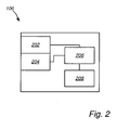
- Fig. 2 shows internal components of the control unit 106.
- the control unit 106 comprises a receiver 202, a transmitter 204, a processing unit 206 and a memory 208.
- the receiver 202 may for example be arranged to receive a capacitance value C of the capacitor 102 and a required energy level W need .
- the transmitter 204 may, for example, be arranged to transmit a signal pertaining to an adjusted charge voltage to the adjustable voltage regulator 104.
- the processing unit 206 which may be a central processing unit is arranged to adjust a charge voltage of the capacitor 102 according to embodiments of the present invention.
- the memory 208 may store computer-readable instructions which, when loaded and read by the processing unit 106, causes the processing unit 106 to carry out a method according to embodiments of the invention.
- a capacitance value C of the capacitor 102 is received.
- the capacitance value C may be received by the receiver 202 of the control unit 106.
- the capacitance value C may be determined based on measurements made on the capacitor 102 as is further described below.
- the capacitance value C may be received from a database. If so, the capacitance value may be determined based on information pertaining to the variation of the capacitance value C as a function of time and/or temperature.
- step S106 a value of the required energy level W need is received.
- the required energy level W need may be received by the receiver 202.
- the required energy level W need may for example be received from a database or from a user input.
- step S108 the charge voltage V C of the capacitor 102 is adjusted.
- An appropriate charge voltage V C may for example be determined by the processing unit 206 of the control unit 106. Further, a signal relating to the determined charge voltage V C may be sent to the adjustable voltage regulator 104, via transmitter 204 of the control unit 106. The adjustable voltage regulator 104 may apply a voltage level across the capacitor 102 corresponding to the adjusted charge voltage. The charge voltage V C is adjusted based on the capacitance value C received in step S102 and the value of the required energy level W need received in step S106.
- the method may further comprise a step S104 of receiving a conductance value G of the capacitor 102.
- the step S108 of adjusting the charge voltage V C may further comprise adjusting the charge voltage based on the conductance value G. This is particularly useful for long lifetimes of the capacitor 102 since the conductance G decreases upon aging of the capacitor 102.
- W need is a known constant
- W stored is a function of the charge voltage V C .
- the charge voltage V C may also be thought of as the initial voltage across the capacitor 102 prior to discharging.
- the energy losses W ESR in the capacitor 102 depends on the discharge current, i(t) say, which flows from the capacitor 102 during discharging.
- the discharge current i(t) is a function of time since, as the voltage across the capacitor 102 decreases during discharging, the discharge current i(t) increases such that a power P provided to the load 110 is kept constant.
- the above system of equations may for example be solved numerically.
- the capacitance value C does not depend on the charge voltage.
- the inventor has realized that the capacitance value C in fact is an increasing, non-linear, function of the charge voltage.
- the method may therefore comprise receiving the new capacitance value C 1 .
- the iteration may be continued until the energy level W stored stored in the capacitor is essentially equal to the required energy level W need .
- the above iterative algorithm may be carried out by the control unit 106.
- the adjusting of the charge voltage may be performed in cycles. More specifically, the steps S102, S106, S108 and S104, where applicable, may be carried out periodically, such as once every day.
- the cycles may have a predetermined period. In one embodiment the period of the cycles is between about 1 second and about 24 hours.
- the period of the cycles may be determined based on the temperature. More precisely, the control unit 106 may receive, for example via the receiver 202, a temperature value of ambient temperature. The control unit 106 may then determine a period of the cycles based on the received temperature value. The determination may be carried out by the processing unit 206.
- the method may further comprise determining the capacitance value C of the capacitor 102.
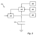
- Fig. 3 illustrates an arrangement 300 which may be used to determine the capacitance value C.
- the arrangement 300 comprises a capacitor 102 which is connected to a power net via an adjustable voltage regulator 104.
- a control unit 106 is connected to the adjustable voltage regulator 104 and is arranged to transmit a signal relating to an adjusted charge voltage to the adjustable voltage regulator 104.
- the control unit 106 is further wired or wirelessly connected to a database 302.
- the database 302 may comprise information pertaining to variation of the capacitance value C as a function of time and/or temperature.
- the information may pertain to the decrease of the capacitance value C due to aging.
- the information may be stored in a table or in the form of a graph or curve.
- the information may be based on calibration experiments which previously have been performed on capacitors.
- the control unit 106 is arranged to receive information pertaining to variation of the capacitance value C as a function of time and/or temperature from a curve or a table.
- the control unit 106 may further be connected to a time measuring means 306 and a temperature gauge 304.
- the time measuring means 306 may for example provide the control unit 106 with a current time and the temperature gauge 304 may provide the control unit 106 with a current temperature.
- the control unit 108 may determine the capacitance value C of the capacitor 102 as the capacitance value of the curve or table that corresponds to a current time and/or temperature.
- Fig. 3 may mutatis mutandis be used to determine a conductance value G of the capacitor.
- Fig. 4 shows an alternative arrangement 400 which may be used to determine the capacitance value C of the capacitor 102.
- the arrangement comprises a capacitor 102 which is connected to a power net via an adjustable voltage regulator 104.
- a control unit 106 is connected to the adjustable voltage regulator 104 and may transmit a signal relating to an adjusted charge voltage to the adjustable voltage regulator 104 as previously disclosed.
- the control unit 106 is further arranged to send a signal to the adjustable voltage regulator 104 instructing the adjustable voltage regulator 104 to provide a charge current to the capacitor 102.
- the control unit 106 is further arranged to measure a voltage across the capacitor 102.
- the arrangement 400 may further comprise a load 402 such as a resistive load or an active current sink, being connected in parallel to the capacitor 102.
- the load 402 is arranged to be turned on and off.
- the control unit 106 may be arranged to turn the load 402 on and off via a switch.
- the arrangement 400 may comprise an arrangement 404 for measuring a charge current.
- the charge current measuring arrangement 404 may be arranged in the circuit between the adjustable voltage regulator 104 and the capacitor 102. Further, the arrangement 404 may be connected to the control unit 106.
- the arrangement 400 may comprise an arrangement 406 for measuring a discharge current.
- the discharge current measuring arrangement 406 is preferably connected in series with the load 402. The arrangement 406 is further connected to the control unit 106.
- the current measuring arrangements 404 and 406 may comprise a high precision resistor and the current may be measured by measuring the voltage across the high precision resistor. The measuring of the voltage across the high precision resistor may be carried out by the control unit 106.
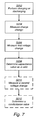
- a step S202 one of charging and discharging of the capacitor 102 is performed.
- the charging may be performed by providing a charging current to the capacitor 102.
- the control unit 106 may instruct the adjustable voltage regulator 104 to provide a charging current to the capacitor 102.
- the discharging may be performed by turning on the load 402 being connected in parallel with the capacitor 102.
- the load 402 may for example be turned on by the control unit 106. Upon activation of the load 402, a discharging current is caused to flow from the capacitor 102 through the load 402.
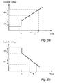
- Figs 5a and 5b illustrate the voltage across the capacitor 102 during charging and discharging, respectively.
- the charging or discharging is initiated at a first time point t 0 .
- a charging current or a discharging current starts to flow to or from the capacitor 102.
- ⁇ V 2 there will be a jump ⁇ V 2 in the voltage across the capacitor 102 at the first time point t 0 . This is due to an ohmic voltage drop caused by the ESR in the capacitor 102 when a charging or discharging current starts to flow to or from the capacitor 102.
- the charge of the capacitor 102 increases or decreases depending on if the capacitor is charged or discharged.
- the charge change ⁇ Q T of the capacitor during a time period T is given by the integral of the current to or from the capacitor 102 during the time period T.
- the time period T is assumed to occur after time t 0 .
- the voltage across the capacitor 102 increases or decreases after time t 0 depending on whether the capacitor 102 is being charged or discharged. In particular, there is a first voltage change ⁇ V 1 across the voltage during the time period T.
- the charge change ⁇ Q T during the time period T is measured.
- the charge change ⁇ Q T may for example be measured by the control unit 106 via the charge current measuring arrangement 404 or the discharge current measuring arrangement 406. More specifically, the charge change ⁇ Q T may be measured by measuring and integrating the charge or discharge current during the time period T.
- the first voltage change ⁇ V 1 across the voltage during the time period T is measured.
- the first voltage change ⁇ V 1 may for example be measured by the control unit.
- the time period T may be any time period of charging or discharging occurring after time t 0 .
- the time period T is as long as possible to minimize measurement uncertainty.
- the method may further comprise a step S210 of measuring a second voltage change corresponding to the jump ⁇ V 2 in the voltage across the capacitor 102 at the first time point to.
- the measuring may be performed by the control unit 106.
- the conductance value G of the capacitor 102 may be determined as the ratio between the known current value and the measured second voltage change ⁇ V 2 .
- the conductance value G may be determined by the control unit 106.
- the charging current or the discharging current corresponds to a constant current value
- the voltage across the capacitor 102 increases or decreases linearly as a function of time during charging or discharging, as illustrated in Figs. 5a and 5b . If so, the rate of increase or decrease of the voltage across the capacitor 102 corresponds to the capacitance value C.
- the step 208 of determining the capacitance value C simplifies to determining a gradient of the voltage across the capacitor 102 during charging or discharging. The determination and the measuring of the voltage across the capacitor 102 may be performed by the control unit 106.
Landscapes
- Engineering & Computer Science (AREA)
- Power Engineering (AREA)
- Charge And Discharge Circuits For Batteries Or The Like (AREA)
- Control Of Electrical Variables (AREA)
- Secondary Cells (AREA)
Description
- The present invention generally relates to the field of charging of capacitors in systems having a charging part and a discharging part. In particular, it relates to a method and arrangements for adjusting the charge voltage of a capacitor in such systems.
- Electrochemical double layer capacitors (EDLCs), also known as ultra capacitors or super capacitors, are often used as energy storage devices in electronic circuits. For example EDLCs may be used as a power back-up in a system.
- A problem with EDLCs is that they have a limited lifetime in that the capacitance and conductance decrease due to electrochemical reactions. The limited lifetime of the EDLCs is particularly problematic when the EDLCs are used in applications with requirements on long product lifetimes. The aging of the EDLCs is influenced by temperature and voltage. Increasing the voltage and temperature will exponentially accelerate the electrochemical reactions and thus leading to a decrease in capacitance and conductance. The lifetime of an EDLC may be defined as the time until capacitance has decreased to 50% of its initial value and the resistance has increased to 300% of its initial value.
- One approach to compensate for the aging of the EDLCs has been to use a capacitor having a high initial capacitance. This approach is disadvantageous in that, initially, more energy is stored in the capacitor than needed. This approach is further disadvantageous in that large capacitors are expensive and that charging of large capacitors to a high voltage level requires a larger and more expensive power supply circuit. Further, the charging of a large capacitor is time consuming.
-
JP2005117792A - The solution of cooling the EDLCs to extend the lifetime as disclosed in
JP2005117792 - In view of the above, it is thus an object of the present invention to provide a method and arrangements for extending the lifetime of a capacitor which is used as a power back-up in a system.
- According to a first aspect of the invention, the above object is achieved by a method for adjusting a charge voltage of a capacitor in a system having a charging part associated with the charge voltage and a discharging part having a required energy level Wneed, the charge voltage being related to an energy level Wstored stored in said capacitor, comprising: receiving a capacitance value of the capacitor; receiving a value of the required energy level Wneed; and adjusting the charge voltage of the capacitor based on said capacitance value and said value of the required energy level Wneed such that the energy level Wstored stored in said capacitor is kept essentially constant.
- The energy stored in a capacitor Wstored is proportional to the capacitance value and to the square of the voltage across the capacitor. Due to aging, the capacitance value decreases over time. Accordingly, if the charge voltage is kept constant, the energy stored in the capacitor Wstored decreases over time, and after a while the energy Wstored stored in the capacitor will be lower than the required energy level Wneed. With the method of the invention, however, the charge voltage is adjusted to compensate for the aging of the capacitor. The charge voltage is adjusted such that the energy level Wstored stored in the capacitor is kept essentially constant. Thus, as the capacitance decreases due to aging of the capacitor, the charge voltage will be increased and the energy level Wstorea stored in the capacitor may be kept above the required energy level Wneed. The lifetime of the capacitor is thereby increased. Moreover, since the charge voltage at any time may be chosen to be as low as possible while still keeping the energy level stored in the capacitor at a level which exceeds the required energy level Wneed the aging of the capacitor is slowed down. Further, the time taken to charge the capacitor is in this way reduced.
- The energy level Wstored stored in the capacitor is preferably larger than or equal to the required energy level Wneed.
- The capacitor may be an Electrochemical Double Layer Capacitor, EDLC.
- The method may further comprise receiving a conductance value of the capacitor, said conductance value being related to an ohmic voltage drop, and wherein said adjusting the charge voltage of the capacitor is further based on said conductance value to compensate for said ohmic voltage drop. This is particularly advantageous for applications requiring a long lifetime of the capacitor since the conductance decreases with time and the ohmic voltage drop thereby increases with time. By ohmic voltage drop is meant a drop in voltage caused by a voltage being generated across a resistive component in the capacitor when a current starts to flow from the capacitor to the discharging part of the system
- The method may further comprise iterating the steps of receiving a capacitance value of the capacitor, and adjusting the charge voltage of the capacitor based on the capacitance value and the value of the required energy level Wneed until the energy level Wstored stored in the capacitor is essentially equal to the required energy level Wneed. This is advantageous in that a non-linear dependence of the capacitance on the charge voltage may be taken into account.
- The acts of receiving a capacitance value, receiving a value of the required energy level Wneed, and adjusting the charge voltage may be performed in cycles. For example, the adjustment of the charge voltage may be performed once a day or once every second. This is advantageous in that the charge voltage may be adjusted periodically to ensure that the energy level stored in the capacitor is kept essentially constant.
- The method may further comprise receiving a temperature value of an ambient temperature, and determining a period of the cycles based on the temperature value. The temperature influences the aging of the capacitor. Thus, for high temperatures, the capacitance decreases rapidly and the adjustment is advantageously carried out more often than for low temperatures.
- The method may further comprise determining the capacitance value of the capacitor. In one embodiment, the act of determining the capacitance value of the capacitor may comprise: performing one of charging or discharging of the capacitor by providing a charging current to the capacitor, or connecting a load in parallel with the capacitor, such that thereby a discharging current is caused to flow from the capacitor, wherein the charging or discharging is initiated at a first time point; measuring a charge change of the capacitor during a time period when the capacitor is charged or discharged, wherein the time period occurs after the first time point; measuring a first voltage change across the capacitor during the same time period; and determining the capacitance value as a ratio between the measured charge change and the measured first voltage change. This is advantageous in that it enables an accurate capacitance value of the capacitance to be obtained by performing direct measurements on the capacitor.
- In case the charging current or the discharging current has a known current value at the first time point, the method may further comprise: measuring a second voltage change occurring at the first time point, the second voltage change being related to a voltage across a resistive component in the capacitor caused by the charging current or the discharging current; and determining a conductance value of the capacitor as the ratio between the known current value and the measured second voltage change. This is advantageous in that also the conductance value may be obtained by direct measurements so that the ohmic voltage drop may be taken into account when adjusting the charge voltage.
- The charging current or the discharging current may correspond to a constant current value, and the act of determining the capacitance value as a ratio may comprise determining a gradient of a measured voltage across the capacitor during charging or discharging of the capacitor. This is advantageous in that the determination of the capacitance value simplifies to determining a gradient of a measured voltage across the capacitor.
- In one embodiment, the act of receiving a capacitance value of the capacitor comprises receiving information pertaining to variation of the capacitance value as a function of time and/or temperature from a curve or a table; and determining the capacitance value of the capacitor as the capacitance value of the curve or table that corresponds to a current time and/or temperature. This is advantageous in that the capacitance value may be determined in a simple way using a low amount of processing power.
- According to a second aspect of the invention, the object is achieved by a control unit for adjusting a charge voltage of a capacitor in a system having a charging part associated with the charge voltage and a discharging part having a required energy level Wneed, the charge voltage being related to an energy level Wstored stored in said capacitor. The control unit comprises a receiver arranged to receive a capacitance value of the capacitor; and a value of the required energy level Wneed; a processing unit arranged to adjust the charge voltage of the capacitor based on said capacitance value and said value of the energy level Wneed such that the energy level Wstored stored in said capacitor is kept essentially constant; and a transmitter arranged to transmit a signal relating to the adjusted charge voltage.
- According to a third aspect of the invention, the object is achieved by an arrangement for adjusting a charge voltage of a capacitor in a system having a charging part associated with the charge voltage and a discharging part having a required energy level Wneed, the charge voltage being related to an energy level Wstored stored in said capacitor. The arrangement comprises a control unit according to the second aspect, and an adjustable voltage regulator which is arranged to receive the signal relating to the adjusted charge voltage from the control unit, and to apply a voltage level across the capacitor corresponding to the adjusted charge voltage.
- According to a fourth aspect of the invention, the object is achieved by a computer program product stored on a non-volatile computer-readable medium comprising computer program code portions adapted to perform the method according to the first method when loaded and executed on a computer.
- The second, third and fourth aspects may generally have the same features and advantages as the first aspect. It is further noted that the invention relates to all possible combinations of features unless explicitly stated otherwise.
- Generally, all terms used in the claims are to be interpreted according to their ordinary meaning in the technical field, unless explicitly defined otherwise herein. All references to "a/an/the [device, event, message, alarm, parameter, step etc.]" are to be interpreted openly as referring to at least one instance of said device, event, message, alarm, parameter, step etc., unless explicitly stated otherwise. The steps of any method disclosed herein do not have to be performed in the exact order disclosed, unless explicitly stated.
- The above, as well as additional objects, features and advantages of the present invention, will be better understood through the following illustrative and non-limiting detailed description of preferred embodiments of the present invention, with reference to the appended drawings, where the same reference numerals will be used for similar elements, wherein:
-
Fig. 1 is a schematic illustration of a system in which embodiments of the present invention may be used, -
Fig. 2 is a schematic illustration of internal components of a control unit according to embodiments, -
Figs 3-4 are schematic illustrations of arrangements for determining a capacitance value according to embodiments. -
Figs 5a-b are schematic graphs illustrating the capacitor voltage as a function of time during charging and discharging, respectively. -
Figs 6-7 are flow charts of methods according to embodiments. - The present invention will now be described more fully hereinafter with reference to the accompanying drawings, in which currently preferred embodiments of the invention are shown. This invention may, however, be embodied in many different forms and should not be construed as limited to the embodiments set forth herein; rather, these embodiments are provided for thoroughness and completeness, and fully convey the scope of the invention to the skilled person.
-
Fig. 1 illustrates asystem 100 comprising aload 110 and acapacitor 102. Thesystem 100 may be used as a back-up system for powering theload 110. Particularly, thecapacitor 102 may be used as a back-up power source for theload 110. Normally, theload 110 is powered via apower net 118. However, if there is a power fail, the load may be connected to the backupsystem comprising thecapacitor 102, for example by means of aswitch 116. - The
system 100 has a chargingpart 112 and a dischargingpart 114. The dischargingpart 114 is associated with a discharging mode of thecapacitor 102. Particularly, in the discharging mode, thecapacitor 102 is connected to theload 110 to power theload 110. Thecapacitor 102 may be connected to theload 110 via avoltage regulator 108. - The charging
part 112 is associated with a charging mode of thecapacitor 102. In the charging mode, thecapacitor 102 is disconnected from theload 110. When in the charging mode, thecapacitor 102 is charged by means of a charging voltage which is applied across thecapacitor 102. The charging voltage is provided by anadjustable voltage regulator 104. Theadjustable voltage regulator 104 is powered by apower net 120. - Further, the
adjustable voltage regulator 104 is connected to acontrol unit 106. Thecontrol unit 106 is arranged to determine an adjusted charge voltage and to send a signal relating to the adjusted charge voltage to theadjustable voltage regulator 104. - The
capacitor 102 may be an EDLC. Thecapacitor 102 has a capacitance value C. Thecapacitor 102 may store an energy level Wstored which is related to the capacitance C and the voltage VC across thecapacitor 102 according to the formula
- The
load 110 is associated with a required energy level Wneed. The required energy level Wneed is the energy which is needed to back-up theload 110 during a predetermined time period T1. More specifically, the required energy level Wneed is a product of the time T1 and a constant power P required to drive theload 110. Thus, preferably, the energy Wstored stored in thecapacitor 102 is larger than or equal to the required energy level Wneed which is needed to back-up theload 110. - The
capacitor 102 is further associated with a conductance G. More precisely, thecapacitor 102 has an equivalent representation which comprises a capacitive part and a resistive part, the conductance G being the inverse of an equivalent series resistance (ESR) of the resistive part of thecapacitor 102. The equivalent series resistance is due to imperfections within the material of thecapacitor 102. The ESR is related to an ohmic voltage drop VESR of the capacitor. More precisely, as a current is flowing from thecapacitor 102, there will according to Ohm's law be a voltage VESR across the capacitor being equal to the product of the equivalent series resistance and the current flowing from thecapacitor 102. As a result of the ohmic voltage drop VESR of thecapacitor 102, all of the energy stored in the capacitor Wstored may not be discharged to theload 110 when the capacitor is in discharging mode since there will be power losses in the resitive component in the capacitor. More precisely, the energy Wuseable which may be used to power theload 110 is given by
where WESR denotes the energy losses in the ESR of thecapacitor 102. Due to aging of thecapacitor 102, the capacitance C as well as the conductance decreases over time. Mainly two factors influence the aging of thecapacitor 102, namely temperature and voltage. Increasing the voltage VC and temperature will exponentially accelerate electrochemical reaction and thus lead to a decrease in conductance and capacitance. Accordingly, the stored energy Wstored or the useable energy Wuseable decrease with time for a constant charge voltage. -
Fig. 2 shows internal components of thecontrol unit 106. Thecontrol unit 106 comprises areceiver 202, atransmitter 204, aprocessing unit 206 and amemory 208. Thereceiver 202 may for example be arranged to receive a capacitance value C of thecapacitor 102 and a required energy level Wneed. Thetransmitter 204 may, for example, be arranged to transmit a signal pertaining to an adjusted charge voltage to theadjustable voltage regulator 104. Theprocessing unit 206 which may be a central processing unit is arranged to adjust a charge voltage of thecapacitor 102 according to embodiments of the present invention. In particular, thememory 208 may store computer-readable instructions which, when loaded and read by theprocessing unit 106, causes theprocessing unit 106 to carry out a method according to embodiments of the invention. - A method for adjusting a charge voltage of the
capacitor 102 will now be described with respect toFig. 6 ,Fig. 1 andFig. 2 . - In step S102 a capacitance value C of the
capacitor 102 is received. The capacitance value C may be received by thereceiver 202 of thecontrol unit 106. The capacitance value C may be determined based on measurements made on thecapacitor 102 as is further described below. Alternatively, the capacitance value C may be received from a database. If so, the capacitance value may be determined based on information pertaining to the variation of the capacitance value C as a function of time and/or temperature. - In step S106, a value of the required energy level Wneed is received. The required energy level Wneed may be received by the
receiver 202. The required energy level Wneed may for example be received from a database or from a user input. - In step S108 the charge voltage VC of the
capacitor 102 is adjusted. An appropriate charge voltage VC may for example be determined by theprocessing unit 206 of thecontrol unit 106. Further, a signal relating to the determined charge voltage VC may be sent to theadjustable voltage regulator 104, viatransmitter 204 of thecontrol unit 106. Theadjustable voltage regulator 104 may apply a voltage level across thecapacitor 102 corresponding to the adjusted charge voltage. The charge voltage VC is adjusted based on the capacitance value C received in step S102 and the value of the required energy level Wneed received in step S106. - The charge voltage VC is adjusted such that the energy level Wneed is kept essentially constant. More specifically, the charge voltage VC may be determined by solving the inequality

where it has been assumed that VC is positive. In order to extend the lifetime of thecapacitor 102 it is desired to keep the charging voltage as low as possible since the aging of the capacitor is accelerated by a high charge voltage. Thus, the charge voltage VC is preferably adjusted according to
- In order to compensate for power losses in the ESR of the
capacitor 102, i.e., to compensate for the ohmic voltage drop VESR which is due to the equivalent series resistance of thecapacitor 102, the method may further comprise a step S104 of receiving a conductance value G of thecapacitor 102. The step S108 of adjusting the charge voltage VC may further comprise adjusting the charge voltage based on the conductance value G. This is particularly useful for long lifetimes of thecapacitor 102 since the conductance G decreases upon aging of thecapacitor 102. The charge voltage VC may for example be adjusted according to the solution of the inequality
Preferably, the charge voltage VC is determined as the solution to the equation
- In the above equation, Wneed is a known constant, and Wstored is a function of the charge voltage VC. The charge voltage VC may also be thought of as the initial voltage across the
capacitor 102 prior to discharging. The energy losses WESR in thecapacitor 102 depends on the discharge current, i(t) say, which flows from thecapacitor 102 during discharging. The discharge current i(t) is a function of time since, as the voltage across thecapacitor 102 decreases during discharging, the discharge current i(t) increases such that a power P provided to theload 110 is kept constant. The energy losses WESR may be expressed as
The discharge current i(t) may be calculated under the assumption that the power P provided to theload 110 is kept constant by solving the system of equations:
where v(t) is the voltage across the capacitive part of the equivalent representation of thecapacitor 102 during discharging, and v(0)=VC. The above system of equations may for example be solved numerically. - In the above, it is has been assumed that the capacitance value C does not depend on the charge voltage. However, the inventor has realized that the capacitance value C in fact is an increasing, non-linear, function of the charge voltage. As an effect, the adjusted charge voltage VC may result in the energy Wstored stored in the
capacitor 102 being larger than Wneed although the energy VC was adjusted by equating Wstored=Wneed according to the above. In order to take the dependency of the capacitance C on the charge voltage VC into account, the adjusted charge voltage may be determined by solving theequation 
where C(VC) denotes the capacitance as a function of charge voltage VC. This is a highly non-linear equation which may be solved by an iterative algorithm. The method may thus further comprise iterating the steps of receiving a capacitance value C of the capacitor, and adjusting the charge voltage VC based on the capacitance value C and the value of the require energy level Wneed. More specifically, a start capacitance C0 may be received and a start value VC,0 of the charge voltage may be determined according to
The charge voltage may then be adjusted to the start value VC,0. As the charge voltage is adjusted, the capacitance value C increases to C1=C(VC,0)>C0 since the capacitance value is an increasing function of the charge voltage. The method may therefore comprise receiving the new capacitance value C1. Based on the newly received capacitance value C1 an adjusted charge voltage VC,1 may be determined according to
The above steps of receiving capacitance values may be iterated such that the charge voltage VC,i determined in the i:th iteration is given by
where Ci is the capacitance received during the i:th iteration. The iteration may be continued until the energy level Wstored stored in the capacitor is essentially equal to the required energy level Wneed. The iteration may be terminated when a predetermined criteria is met. For example the iteration may be continued until
for some predetermined tolerance value ε > 0. The above iterative algorithm may be carried out by thecontrol unit 106. - The above iterative approach also applies mutatis mutandis to the case where the equivalent series resistance ESR is taken into account.
- The adjusting of the charge voltage may be performed in cycles. More specifically, the steps S102, S106, S108 and S104, where applicable, may be carried out periodically, such as once every day. The cycles may have a predetermined period. In one embodiment the period of the cycles is between about 1 second and about 24 hours.
- Since the aging of the capacitors depends on the temperature the period of the cycles may be determined based on the temperature. More precisely, the
control unit 106 may receive, for example via thereceiver 202, a temperature value of ambient temperature. Thecontrol unit 106 may then determine a period of the cycles based on the received temperature value. The determination may be carried out by theprocessing unit 206. - The method may further comprise determining the capacitance value C of the
capacitor 102.Fig. 3 illustrates anarrangement 300 which may be used to determine the capacitance value C. Thearrangement 300 comprises acapacitor 102 which is connected to a power net via anadjustable voltage regulator 104. Acontrol unit 106 is connected to theadjustable voltage regulator 104 and is arranged to transmit a signal relating to an adjusted charge voltage to theadjustable voltage regulator 104. - The
control unit 106 is further wired or wirelessly connected to adatabase 302. Thedatabase 302 may comprise information pertaining to variation of the capacitance value C as a function of time and/or temperature. In particular, the information may pertain to the decrease of the capacitance value C due to aging. For example, the information may be stored in a table or in the form of a graph or curve. The information may be based on calibration experiments which previously have been performed on capacitors. In this way, thecontrol unit 106 is arranged to receive information pertaining to variation of the capacitance value C as a function of time and/or temperature from a curve or a table. - The
control unit 106 may further be connected to a time measuring means 306 and atemperature gauge 304. The time measuring means 306 may for example provide thecontrol unit 106 with a current time and thetemperature gauge 304 may provide thecontrol unit 106 with a current temperature. Based on the current time and/or temperature and on the received information from thedatabase 302, thecontrol unit 108 may determine the capacitance value C of thecapacitor 102 as the capacitance value of the curve or table that corresponds to a current time and/or temperature. - The arrangement of
Fig. 3 may mutatis mutandis be used to determine a conductance value G of the capacitor. -
Fig. 4 shows analternative arrangement 400 which may be used to determine the capacitance value C of thecapacitor 102. The arrangement comprises acapacitor 102 which is connected to a power net via anadjustable voltage regulator 104. Acontrol unit 106 is connected to theadjustable voltage regulator 104 and may transmit a signal relating to an adjusted charge voltage to theadjustable voltage regulator 104 as previously disclosed. Thecontrol unit 106 is further arranged to send a signal to theadjustable voltage regulator 104 instructing theadjustable voltage regulator 104 to provide a charge current to thecapacitor 102. Thecontrol unit 106 is further arranged to measure a voltage across thecapacitor 102. - The
arrangement 400 may further comprise aload 402 such as a resistive load or an active current sink, being connected in parallel to thecapacitor 102. Theload 402 is arranged to be turned on and off. For example, thecontrol unit 106 may be arranged to turn theload 402 on and off via a switch. - Further the
arrangement 400 may comprise anarrangement 404 for measuring a charge current. The chargecurrent measuring arrangement 404 may be arranged in the circuit between theadjustable voltage regulator 104 and thecapacitor 102. Further, thearrangement 404 may be connected to thecontrol unit 106. Similarly, thearrangement 400 may comprise anarrangement 406 for measuring a discharge current. The dischargecurrent measuring arrangement 406 is preferably connected in series with theload 402. Thearrangement 406 is further connected to thecontrol unit 106. For example thecurrent measuring arrangements control unit 106. - A method for determining the capacitance value C of the
capacitor 102 will now be described with respect toFig. 7 andFigs 4 and5 . - In a step S202 one of charging and discharging of the
capacitor 102 is performed. The charging may be performed by providing a charging current to thecapacitor 102. For example, thecontrol unit 106 may instruct theadjustable voltage regulator 104 to provide a charging current to thecapacitor 102. The discharging may be performed by turning on theload 402 being connected in parallel with thecapacitor 102. Theload 402 may for example be turned on by thecontrol unit 106. Upon activation of theload 402, a discharging current is caused to flow from thecapacitor 102 through theload 402. -
Figs 5a and 5b illustrate the voltage across thecapacitor 102 during charging and discharging, respectively. The charging or discharging is initiated at a first time point t0. At the first time point t0, a charging current or a discharging current starts to flow to or from thecapacitor 102. As a consequence, there will be a jump ΔV2 in the voltage across thecapacitor 102 at the first time point t0. This is due to an ohmic voltage drop caused by the ESR in thecapacitor 102 when a charging or discharging current starts to flow to or from thecapacitor 102. - As time goes by, the charge of the
capacitor 102 increases or decreases depending on if the capacitor is charged or discharged. The charge change ΔQT of the capacitor during a time period T is given by the integral of the current to or from thecapacitor 102 during the time period T. The time period T is assumed to occur after time t0. Further, the voltage across thecapacitor 102 increases or decreases after time t0 depending on whether thecapacitor 102 is being charged or discharged. In particular, there is a first voltage change ΔV1 across the voltage during the time period T. - In a step S204, the charge change ΔQT during the time period T is measured. The charge change ΔQT may for example be measured by the
control unit 106 via the chargecurrent measuring arrangement 404 or the dischargecurrent measuring arrangement 406. More specifically, the charge change ΔQT may be measured by measuring and integrating the charge or discharge current during the time period T. - In a step S206, the first voltage change ΔV1 across the voltage during the time period T is measured. The first voltage change ΔV1 may for example be measured by the control unit. In principle, the time period T may be any time period of charging or discharging occurring after time t0. Preferably, the time period T is as long as possible to minimize measurement uncertainty.
- In a step S208, the capacitance value C of the
capacitor 102 is determined as a ratio between the measured charge change ΔQT and the measured first voltage change ΔV1, viz.
- In case the charging current or the discharging current has a known current value at the first time point, the method may further comprise a step S210 of measuring a second voltage change corresponding to the jump ΔV2 in the voltage across the
capacitor 102 at the first time point to. The measuring may be performed by thecontrol unit 106. - In a step S212, the conductance value G of the
capacitor 102 may be determined as the ratio between the known current value and the measured second voltage change ΔV2. The conductance value G may be determined by thecontrol unit 106. - In case the charging current or the discharging current corresponds to a constant current value, the voltage across the
capacitor 102 increases or decreases linearly as a function of time during charging or discharging, as illustrated inFigs. 5a and 5b . If so, the rate of increase or decrease of the voltage across thecapacitor 102 corresponds to the capacitance value C. In this case, thestep 208 of determining the capacitance value C simplifies to determining a gradient of the voltage across thecapacitor 102 during charging or discharging. The determination and the measuring of the voltage across thecapacitor 102 may be performed by thecontrol unit 106. - It will be appreciated that a person skilled in the art can modify the above-described embodiments in many ways and still use the advantages of the invention as shown in the embodiments above. For example, the embodiments for determining the capacitance disclosed with respect to
Figs 3-4 may be combined such that the capacitance and/or conductance sometimes is determined by measuring on the capacitor and sometimes determined based on information received from a database. Thus, the invention should not be limited to the shown embodiments but should only be defined by the appended claims.
Claims (15)
- A method for adjusting a charge voltage of a capacitor in a system having a charging part associated with the charge voltage and a discharging part having a required energy level Wneed, the charge voltage being related to an energy level Wstored stored in said capacitor, comprising
receiving a capacitance value of the capacitor;
receiving a value of the required energy level Wneed; and
adjusting the charge voltage of the capacitor based on said capacitance value and said value of the required energy level Wneed such that the energy level Wstored stored in said capacitor is kept essentially constant. - The method according to claim 1, wherein the capacitor is an Electrochemical Double Layer Capacitor, EDLC.
- The method according to claim 1, further comprising
receiving a conductance value of the capacitor, said conductance value being related to an ohmic voltage drop,
wherein said adjusting the charge voltage of the capacitor is further based on said conductance value to compensate for said ohmic voltage drop. - The method according to claim 1, wherein the energy level Wstored stored in the capacitor is larger than or equal to the required energy level Wneed.
- The method according to claim 1, further comprising
iterating the steps of receiving a capacitance value of the capacitor, and adjusting the charge voltage of the capacitor based on the capacitance value and the value of the required energy level Wneed until the energy level Wstored stored in the capacitor is essentially equal to the required energy level Wneed. - The method according to claim 1, wherein the acts of receiving a capacitance value, receiving a value of the required energy level Wneed, and adjusting the charge voltage are performed in cycles.
- The method according to claim 6, further comprising receiving a temperature value of an ambient temperature, and determining a period of the cycles based on the temperature value.
- The method according to claim 1, further comprising determining the capacitance value of the capacitor.
- The method according to claim 8, wherein the act of determining the capacitance value of the capacitor comprises
performing one of charging or discharging of the capacitor byproviding a charging current to the capacitor, orconnecting a load in parallel with the capacitor, such that thereby a discharging current is caused to flow from the capacitor, wherein the charging or discharging is initiated at a first time point, measuring a charge change of the capacitor during a time period when the capacitor is charged or discharged, wherein the time period occurs after the first time point,measuring a first voltage change across the capacitor during the same time period, and
determining the capacitance value as a ratio between the measured charge change and the measured first voltage change. - The method according to claim 9, wherein the charging current or the discharging current has a known current value at the first time point, the method further comprising:measuring a second voltage change occurring at the first time point, the second voltage change being related to a voltage across a resistive component in the capacitor caused by the charging current or the discharging current, anddetermining a conductance value of the capacitor as the ratio between the known current value and the measured second voltage change.
- The method according to claim 9, wherein the charging current or the discharging current corresponds to a constant current value, and wherein the act of determining the capacitance value as a ratio comprises determining a gradient of a measured voltage across the capacitor during charging or discharging of the capacitor.
- The method according to claim 8, wherein the act of receiving a capacitance value of the capacitor comprises
receiving information pertaining to variation of the capacitance value as a function of time and/or temperature from a curve or a table,
determining the capacitance value of the capacitor as the capacitance value of the curve or table that corresponds to a current time and/or temperature. - A control unit for adjusting a charge voltage of a capacitor in a system having a charging part associated with the charge voltage and a discharging part having a required energy level Wneed, the charge voltage being related to an energy level Wstored stored in said capacitor, comprising
a receiver arranged to receive a capacitance value of the capacitor; and a value of the required energy level Wneed;
a processing unit arranged to adjust the charge voltage of the capacitor based on said capacitance value and said value of the energy level Wneed such that the energy level Wstored stored in said capacitor is kept essentially constant; and
a transmitter arranged to transmit a signal relating to the adjusted charge voltage. - An arrangement for adjusting a charge voltage of a capacitor in a system having a charging part associated with the charge voltage and a
a control unit according to claim 13, and
an adjustable voltage regulator which is arranged to receive the signal relating to the adjusted charge voltage from the control unit, and to apply a voltage level across the capacitor corresponding to the adjusted charge voltage. - A computer program product stored on a non-volatile computer-readable medium comprising computer program code portions adapted to perform the method according to any of claims 1-12 when loaded and executed on a computer.
Applications Claiming Priority (1)
| Application Number | Priority Date | Filing Date | Title |
|---|---|---|---|
| PCT/EP2012/050563 WO2013107497A1 (en) | 2012-01-16 | 2012-01-16 | Adjustment of a capacitor charge voltage |
Publications (2)
| Publication Number | Publication Date |
|---|---|
| EP2805401A1 EP2805401A1 (en) | 2014-11-26 |
| EP2805401B1 true EP2805401B1 (en) | 2015-12-30 |
Family
ID=45558688
Family Applications (1)
| Application Number | Title | Priority Date | Filing Date |
|---|---|---|---|
| EP12701847.1A Active EP2805401B1 (en) | 2012-01-16 | 2012-01-16 | Adjustment of a capacitor charge voltage |
Country Status (6)
| Country | Link |
|---|---|
| US (1) | US20150340882A1 (en) |
| EP (1) | EP2805401B1 (en) |
| CN (1) | CN104054233B (en) |
| AU (1) | AU2012366914B2 (en) |
| IN (1) | IN2014KN01565A (en) |
| WO (1) | WO2013107497A1 (en) |
Families Citing this family (12)
| Publication number | Priority date | Publication date | Assignee | Title |
|---|---|---|---|---|
| JP6526567B2 (en) * | 2012-12-24 | 2019-06-05 | マグナ クロージャーズ インコーポレイテッド | Collision management system and method in electronic latch of automobile closure device |
| CN104716814B (en) * | 2013-12-13 | 2018-10-26 | 光宝电子(广州)有限公司 | Power system and its control method |
| WO2015183250A1 (en) * | 2014-05-28 | 2015-12-03 | Schneider Electric Buildings Llc | Estimation of the remaining lifetime of a supercapacitor |
| US20160202749A1 (en) * | 2015-01-13 | 2016-07-14 | Netlist, Inc. | System and method for determining charge of a secondary power supply for a memory system |
| EP3160000B1 (en) * | 2015-10-20 | 2020-12-23 | Siemens Aktiengesellschaft | Adjusting an operating point of an electrical energy storage device which is ready for operation |
| FI128211B (en) | 2017-05-23 | 2019-12-31 | Abloy Oy | Electric lock arrangement |
| US10620247B2 (en) * | 2017-09-27 | 2020-04-14 | Quanta Computer Inc. | System and method to detect capacitance of a power supply unit |
| US10886837B2 (en) * | 2018-03-09 | 2021-01-05 | The Johns Hopkins University | Virtual capacitor |
| US11870280B2 (en) * | 2018-09-19 | 2024-01-09 | Johnson Controls Tyco IP Holdings LLP | Systems and methods for controlling super capacitor charge voltage to extend super capacitor life |
| EP3745145A1 (en) * | 2019-05-28 | 2020-12-02 | Schneider Electric Industries SAS | Estimation of the remaining useful life of capacitors |
| US11594896B2 (en) * | 2019-10-22 | 2023-02-28 | John Holtzman | Charger extension device |
| US11878600B2 (en) * | 2021-03-31 | 2024-01-23 | Lear Corporation | Vehicle on-board charger with variable DC-link voltage |
Family Cites Families (17)
| Publication number | Priority date | Publication date | Assignee | Title |
|---|---|---|---|---|
| JP3135500B2 (en) * | 1996-06-27 | 2001-02-13 | ウエスト電気株式会社 | Strobe device and photo camera incorporating the strobe device |
| JPH1015670A (en) * | 1996-07-03 | 1998-01-20 | Nippon Avionics Co Ltd | Method for compensating capacitor capacity in capacity type welding power source, and circuit therefor |
| DE10305357B4 (en) * | 2003-02-10 | 2005-12-22 | Siemens Ag | Device for supplying power to a two-voltage vehicle electrical system equipped with safety-relevant components |
| JP4385664B2 (en) * | 2003-07-08 | 2009-12-16 | パナソニック株式会社 | Vehicle power supply |
| JP2005117792A (en) * | 2003-10-08 | 2005-04-28 | Toshiba Corp | Apparatus and method for controlling power |
| JP4367374B2 (en) * | 2005-05-16 | 2009-11-18 | パナソニック株式会社 | Power storage device |
| JP4449940B2 (en) * | 2006-05-16 | 2010-04-14 | トヨタ自動車株式会社 | Dual power supply system for vehicles |
| US8493036B2 (en) * | 2006-10-21 | 2013-07-23 | Advanced Analogic Technologies, Inc. | Controllable charge paths, and related methods |
| JP2008017691A (en) * | 2007-07-24 | 2008-01-24 | Toshiba Corp | Monitoring device of electric double-layer capacitor system |
| JP5018448B2 (en) * | 2007-12-18 | 2012-09-05 | パナソニック株式会社 | Power storage device |
| WO2009087956A1 (en) * | 2008-01-07 | 2009-07-16 | Panasonic Corporation | Electricity accumulating device |
| US8552687B2 (en) * | 2008-06-05 | 2013-10-08 | GM Global Technology Operations LLC | Method and system for characterizing a battery |
| TWI472120B (en) * | 2008-07-23 | 2015-02-01 | Koninkl Philips Electronics Nv | Method and charger for charging super-capacitor |
| US8058744B2 (en) * | 2008-10-23 | 2011-11-15 | GM Global Technology Operations LLC | Electrical system and automotive drive system having an on-demand boost converter, and related operating methods |
| DE102009018098A1 (en) * | 2009-04-20 | 2010-10-21 | Austriamicrosystems Ag | Charging circuit for a charge storage and method for loading such |
| EP3101765B1 (en) * | 2010-06-28 | 2018-02-14 | Maxwell Technologies, Inc. | Maximizing life of capacitors in series modules |
| JP2012137341A (en) * | 2010-12-24 | 2012-07-19 | Toshiba Corp | Electronic apparatus and capacitance detection method for capacitor in electronic apparatus |
-
2012
- 2012-01-16 WO PCT/EP2012/050563 patent/WO2013107497A1/en active Application Filing
- 2012-01-16 AU AU2012366914A patent/AU2012366914B2/en active Active
- 2012-01-16 IN IN1565KON2014 patent/IN2014KN01565A/en unknown
- 2012-01-16 EP EP12701847.1A patent/EP2805401B1/en active Active
- 2012-01-16 US US14/372,144 patent/US20150340882A1/en not_active Abandoned
- 2012-01-16 CN CN201280066968.3A patent/CN104054233B/en active Active
Also Published As
| Publication number | Publication date |
|---|---|
| EP2805401A1 (en) | 2014-11-26 |
| IN2014KN01565A (en) | 2015-10-23 |
| WO2013107497A1 (en) | 2013-07-25 |
| AU2012366914B2 (en) | 2017-01-05 |
| US20150340882A1 (en) | 2015-11-26 |
| CN104054233B (en) | 2017-05-03 |
| CN104054233A (en) | 2014-09-17 |
| AU2012366914A1 (en) | 2014-07-10 |
Similar Documents
| Publication | Publication Date | Title |
|---|---|---|
| EP2805401B1 (en) | Adjustment of a capacitor charge voltage | |
| JP5897701B2 (en) | Battery state estimation device | |
| US10191117B2 (en) | Battery remaining power predicting device and battery pack | |
| CN110515002B (en) | Battery capacity monitor | |
| JP6824614B2 (en) | Deterioration judgment device and deterioration judgment method | |
| CN111697275B (en) | Semiconductor device and battery pack | |
| US9052368B2 (en) | Negative peak voltage detection for enhanced FuelGauge empty voltage prediction | |
| CN105634051B (en) | Remaining battery level predicting device and battery pack | |
| EP3576250B1 (en) | Vehicle-mounted emergency power supply device | |
| KR20160110211A (en) | Battery remaining power predicting device and battery pack | |
| US9891287B2 (en) | Temperature-compensated state of charge estimation for rechargeable batteries | |
| US10823497B2 (en) | Insulation-time determining device for a thermally insulated container | |
| US10693310B2 (en) | Hiccup charger | |
| WO2015183250A1 (en) | Estimation of the remaining lifetime of a supercapacitor | |
| JP6386351B2 (en) | Calculation method of charge rate of storage battery | |
| CN110780217B (en) | Semiconductor device and method for detecting remaining battery level | |
| KR20160046707A (en) | Reported state-of-charge scaling | |
| JP7042413B2 (en) | Internal resistance detector and power supply | |
| JP2016065844A (en) | Battery system control apparatus and control method of battery system | |
| US11275119B2 (en) | Methods and system for a battery | |
| KR102037378B1 (en) | Method and apparatus for estimating SOC in constant current state, battery management system and energy storage system comprising the same | |
| KR20190100065A (en) | Apparatus and method for calculating State Of Charge | |
| Rezzi et al. | Battery management in mobile devices | |
| JP6041528B2 (en) | Capacitance measurement system, capacitance measurement method, capacitor cell degradation state estimation system, and degradation state estimation method | |
| US10770911B1 (en) | Calibrating battery fuel gages |
Legal Events
| Date | Code | Title | Description |
|---|---|---|---|
| PUAI | Public reference made under article 153(3) epc to a published international application that has entered the european phase |
Free format text: ORIGINAL CODE: 0009012 |
|
| 17P | Request for examination filed |
Effective date: 20140808 |
|
| AK | Designated contracting states |
Kind code of ref document: A1 Designated state(s): AL AT BE BG CH CY CZ DE DK EE ES FI FR GB GR HR HU IE IS IT LI LT LU LV MC MK MT NL NO PL PT RO RS SE SI SK SM TR |
|
| DAX | Request for extension of the european patent (deleted) | ||
| GRAP | Despatch of communication of intention to grant a patent |
Free format text: ORIGINAL CODE: EPIDOSNIGR1 |
|
| INTG | Intention to grant announced |
Effective date: 20150703 |
|
| RIN1 | Information on inventor provided before grant (corrected) |
Inventor name: GOETH, FREDRIK |
|
| GRAS | Grant fee paid |
Free format text: ORIGINAL CODE: EPIDOSNIGR3 |
|
| GRAA | (expected) grant |
Free format text: ORIGINAL CODE: 0009210 |
|
| AK | Designated contracting states |
Kind code of ref document: B1 Designated state(s): AL AT BE BG CH CY CZ DE DK EE ES FI FR GB GR HR HU IE IS IT LI LT LU LV MC MK MT NL NO PL PT RO RS SE SI SK SM TR |
|
| REG | Reference to a national code |
Ref country code: GB Ref legal event code: FG4D |
|
| REG | Reference to a national code |
Ref country code: CH Ref legal event code: EP |
|
| REG | Reference to a national code |
Ref country code: AT Ref legal event code: REF Ref document number: 767867 Country of ref document: AT Kind code of ref document: T Effective date: 20160115 |
|
| REG | Reference to a national code |
Ref country code: IE Ref legal event code: FG4D |
|
| REG | Reference to a national code |
Ref country code: DE Ref legal event code: R096 Ref document number: 602012013342 Country of ref document: DE |
|
| REG | Reference to a national code |
Ref country code: LT Ref legal event code: MG4D Ref country code: FR Ref legal event code: PLFP Year of fee payment: 5 |
|
| PG25 | Lapsed in a contracting state [announced via postgrant information from national office to epo] |
Ref country code: HR Free format text: LAPSE BECAUSE OF FAILURE TO SUBMIT A TRANSLATION OF THE DESCRIPTION OR TO PAY THE FEE WITHIN THE PRESCRIBED TIME-LIMIT Effective date: 20151230 Ref country code: NO Free format text: LAPSE BECAUSE OF FAILURE TO SUBMIT A TRANSLATION OF THE DESCRIPTION OR TO PAY THE FEE WITHIN THE PRESCRIBED TIME-LIMIT Effective date: 20160330 Ref country code: LT Free format text: LAPSE BECAUSE OF FAILURE TO SUBMIT A TRANSLATION OF THE DESCRIPTION OR TO PAY THE FEE WITHIN THE PRESCRIBED TIME-LIMIT Effective date: 20151230 |
|
| REG | Reference to a national code |
Ref country code: NL Ref legal event code: MP Effective date: 20151230 |
|
| REG | Reference to a national code |
Ref country code: AT Ref legal event code: MK05 Ref document number: 767867 Country of ref document: AT Kind code of ref document: T Effective date: 20151230 |
|
| PG25 | Lapsed in a contracting state [announced via postgrant information from national office to epo] |
Ref country code: SE Free format text: LAPSE BECAUSE OF FAILURE TO SUBMIT A TRANSLATION OF THE DESCRIPTION OR TO PAY THE FEE WITHIN THE PRESCRIBED TIME-LIMIT Effective date: 20151230 Ref country code: BE Free format text: LAPSE BECAUSE OF NON-PAYMENT OF DUE FEES Effective date: 20160131 Ref country code: FI Free format text: LAPSE BECAUSE OF FAILURE TO SUBMIT A TRANSLATION OF THE DESCRIPTION OR TO PAY THE FEE WITHIN THE PRESCRIBED TIME-LIMIT Effective date: 20151230 Ref country code: LV Free format text: LAPSE BECAUSE OF FAILURE TO SUBMIT A TRANSLATION OF THE DESCRIPTION OR TO PAY THE FEE WITHIN THE PRESCRIBED TIME-LIMIT Effective date: 20151230 Ref country code: RS Free format text: LAPSE BECAUSE OF FAILURE TO SUBMIT A TRANSLATION OF THE DESCRIPTION OR TO PAY THE FEE WITHIN THE PRESCRIBED TIME-LIMIT Effective date: 20151230 Ref country code: GR Free format text: LAPSE BECAUSE OF FAILURE TO SUBMIT A TRANSLATION OF THE DESCRIPTION OR TO PAY THE FEE WITHIN THE PRESCRIBED TIME-LIMIT Effective date: 20160331 |
|
| PG25 | Lapsed in a contracting state [announced via postgrant information from national office to epo] |
Ref country code: NL Free format text: LAPSE BECAUSE OF FAILURE TO SUBMIT A TRANSLATION OF THE DESCRIPTION OR TO PAY THE FEE WITHIN THE PRESCRIBED TIME-LIMIT Effective date: 20151230 |
|
| PG25 | Lapsed in a contracting state [announced via postgrant information from national office to epo] |
Ref country code: CZ Free format text: LAPSE BECAUSE OF FAILURE TO SUBMIT A TRANSLATION OF THE DESCRIPTION OR TO PAY THE FEE WITHIN THE PRESCRIBED TIME-LIMIT Effective date: 20151230 Ref country code: ES Free format text: LAPSE BECAUSE OF FAILURE TO SUBMIT A TRANSLATION OF THE DESCRIPTION OR TO PAY THE FEE WITHIN THE PRESCRIBED TIME-LIMIT Effective date: 20151230 Ref country code: IT Free format text: LAPSE BECAUSE OF FAILURE TO SUBMIT A TRANSLATION OF THE DESCRIPTION OR TO PAY THE FEE WITHIN THE PRESCRIBED TIME-LIMIT Effective date: 20151230 |
|
| PG25 | Lapsed in a contracting state [announced via postgrant information from national office to epo] |
Ref country code: SM Free format text: LAPSE BECAUSE OF FAILURE TO SUBMIT A TRANSLATION OF THE DESCRIPTION OR TO PAY THE FEE WITHIN THE PRESCRIBED TIME-LIMIT Effective date: 20151230 Ref country code: PT Free format text: LAPSE BECAUSE OF FAILURE TO SUBMIT A TRANSLATION OF THE DESCRIPTION OR TO PAY THE FEE WITHIN THE PRESCRIBED TIME-LIMIT Effective date: 20160502 Ref country code: IS Free format text: LAPSE BECAUSE OF FAILURE TO SUBMIT A TRANSLATION OF THE DESCRIPTION OR TO PAY THE FEE WITHIN THE PRESCRIBED TIME-LIMIT Effective date: 20160430 Ref country code: RO Free format text: LAPSE BECAUSE OF FAILURE TO SUBMIT A TRANSLATION OF THE DESCRIPTION OR TO PAY THE FEE WITHIN THE PRESCRIBED TIME-LIMIT Effective date: 20151230 Ref country code: LU Free format text: LAPSE BECAUSE OF FAILURE TO SUBMIT A TRANSLATION OF THE DESCRIPTION OR TO PAY THE FEE WITHIN THE PRESCRIBED TIME-LIMIT Effective date: 20160116 Ref country code: AT Free format text: LAPSE BECAUSE OF FAILURE TO SUBMIT A TRANSLATION OF THE DESCRIPTION OR TO PAY THE FEE WITHIN THE PRESCRIBED TIME-LIMIT Effective date: 20151230 Ref country code: EE Free format text: LAPSE BECAUSE OF FAILURE TO SUBMIT A TRANSLATION OF THE DESCRIPTION OR TO PAY THE FEE WITHIN THE PRESCRIBED TIME-LIMIT Effective date: 20151230 Ref country code: SK Free format text: LAPSE BECAUSE OF FAILURE TO SUBMIT A TRANSLATION OF THE DESCRIPTION OR TO PAY THE FEE WITHIN THE PRESCRIBED TIME-LIMIT Effective date: 20151230 Ref country code: PL Free format text: LAPSE BECAUSE OF FAILURE TO SUBMIT A TRANSLATION OF THE DESCRIPTION OR TO PAY THE FEE WITHIN THE PRESCRIBED TIME-LIMIT Effective date: 20151230 |
|
| REG | Reference to a national code |
Ref country code: CH Ref legal event code: PL |
|
| PG25 | Lapsed in a contracting state [announced via postgrant information from national office to epo] |
Ref country code: MC Free format text: LAPSE BECAUSE OF FAILURE TO SUBMIT A TRANSLATION OF THE DESCRIPTION OR TO PAY THE FEE WITHIN THE PRESCRIBED TIME-LIMIT Effective date: 20151230 |
|
| REG | Reference to a national code |
Ref country code: DE Ref legal event code: R097 Ref document number: 602012013342 Country of ref document: DE |
|
| PG25 | Lapsed in a contracting state [announced via postgrant information from national office to epo] |
Ref country code: LI Free format text: LAPSE BECAUSE OF NON-PAYMENT OF DUE FEES Effective date: 20160131 Ref country code: CH Free format text: LAPSE BECAUSE OF NON-PAYMENT OF DUE FEES Effective date: 20160131 Ref country code: DK Free format text: LAPSE BECAUSE OF FAILURE TO SUBMIT A TRANSLATION OF THE DESCRIPTION OR TO PAY THE FEE WITHIN THE PRESCRIBED TIME-LIMIT Effective date: 20151230 |
|
| REG | Reference to a national code |
Ref country code: IE Ref legal event code: MM4A |
|
| PLBE | No opposition filed within time limit |
Free format text: ORIGINAL CODE: 0009261 |
|
| STAA | Information on the status of an ep patent application or granted ep patent |
Free format text: STATUS: NO OPPOSITION FILED WITHIN TIME LIMIT |
|
| 26N | No opposition filed |
Effective date: 20161003 |
|
| PG25 | Lapsed in a contracting state [announced via postgrant information from national office to epo] |
Ref country code: BE Free format text: LAPSE BECAUSE OF FAILURE TO SUBMIT A TRANSLATION OF THE DESCRIPTION OR TO PAY THE FEE WITHIN THE PRESCRIBED TIME-LIMIT Effective date: 20151230 |
|
| REG | Reference to a national code |
Ref country code: FR Ref legal event code: PLFP Year of fee payment: 6 |
|
| PG25 | Lapsed in a contracting state [announced via postgrant information from national office to epo] |
Ref country code: IE Free format text: LAPSE BECAUSE OF NON-PAYMENT OF DUE FEES Effective date: 20160116 |
|
| PG25 | Lapsed in a contracting state [announced via postgrant information from national office to epo] |
Ref country code: SI Free format text: LAPSE BECAUSE OF FAILURE TO SUBMIT A TRANSLATION OF THE DESCRIPTION OR TO PAY THE FEE WITHIN THE PRESCRIBED TIME-LIMIT Effective date: 20151230 |
|
| PG25 | Lapsed in a contracting state [announced via postgrant information from national office to epo] |
Ref country code: MT Free format text: LAPSE BECAUSE OF FAILURE TO SUBMIT A TRANSLATION OF THE DESCRIPTION OR TO PAY THE FEE WITHIN THE PRESCRIBED TIME-LIMIT Effective date: 20151230 |
|
| REG | Reference to a national code |
Ref country code: FR Ref legal event code: PLFP Year of fee payment: 7 |
|
| PG25 | Lapsed in a contracting state [announced via postgrant information from national office to epo] |
Ref country code: HU Free format text: LAPSE BECAUSE OF FAILURE TO SUBMIT A TRANSLATION OF THE DESCRIPTION OR TO PAY THE FEE WITHIN THE PRESCRIBED TIME-LIMIT; INVALID AB INITIO Effective date: 20120116 |
|
| PG25 | Lapsed in a contracting state [announced via postgrant information from national office to epo] |
Ref country code: CY Free format text: LAPSE BECAUSE OF FAILURE TO SUBMIT A TRANSLATION OF THE DESCRIPTION OR TO PAY THE FEE WITHIN THE PRESCRIBED TIME-LIMIT Effective date: 20151230 Ref country code: MT Free format text: LAPSE BECAUSE OF FAILURE TO SUBMIT A TRANSLATION OF THE DESCRIPTION OR TO PAY THE FEE WITHIN THE PRESCRIBED TIME-LIMIT Effective date: 20160131 Ref country code: MK Free format text: LAPSE BECAUSE OF FAILURE TO SUBMIT A TRANSLATION OF THE DESCRIPTION OR TO PAY THE FEE WITHIN THE PRESCRIBED TIME-LIMIT Effective date: 20151230 |
|
| PG25 | Lapsed in a contracting state [announced via postgrant information from national office to epo] |
Ref country code: BG Free format text: LAPSE BECAUSE OF FAILURE TO SUBMIT A TRANSLATION OF THE DESCRIPTION OR TO PAY THE FEE WITHIN THE PRESCRIBED TIME-LIMIT Effective date: 20151230 |
|
| PG25 | Lapsed in a contracting state [announced via postgrant information from national office to epo] |
Ref country code: AL Free format text: LAPSE BECAUSE OF FAILURE TO SUBMIT A TRANSLATION OF THE DESCRIPTION OR TO PAY THE FEE WITHIN THE PRESCRIBED TIME-LIMIT Effective date: 20151230 Ref country code: TR Free format text: LAPSE BECAUSE OF FAILURE TO SUBMIT A TRANSLATION OF THE DESCRIPTION OR TO PAY THE FEE WITHIN THE PRESCRIBED TIME-LIMIT Effective date: 20151230 |
|
| REG | Reference to a national code |
Ref country code: GB Ref legal event code: S117 Free format text: REQUEST FILED; REQUEST FOR CORRECTION UNDER SECTION 117 FILED ON 04 JULY 2022 |
|
| REG | Reference to a national code |
Ref country code: GB Ref legal event code: S117 Free format text: CORRECTIONS ALLOWED; REQUEST FOR CORRECTION UNDER SECTION 117 FILED ON 4 JULY 2022 WAS ALLOWED ON 3 AUGUST 2022 |
|
| REG | Reference to a national code |
Ref country code: GB Ref legal event code: 732E Free format text: REGISTERED BETWEEN 20220901 AND 20220907 |
|
| REG | Reference to a national code |
Ref country code: DE Ref legal event code: R081 Ref document number: 602012013342 Country of ref document: DE Owner name: SCHNEIDER ELECTRIC BUILDINGS AMERICAS, INC., C, US Free format text: FORMER OWNER: SCHNEIDER ELECTRIC BUILDINGS LLC, NORTH ANDOVER, MA, US |
|
| PGFP | Annual fee paid to national office [announced via postgrant information from national office to epo] |
Ref country code: FR Payment date: 20230124 Year of fee payment: 12 |
|
| PGFP | Annual fee paid to national office [announced via postgrant information from national office to epo] |
Ref country code: DE Payment date: 20240129 Year of fee payment: 13 Ref country code: GB Payment date: 20240123 Year of fee payment: 13 |