EP2802003B1 - Method for providing a gate metal layer of a transistor device - Google Patents
Method for providing a gate metal layer of a transistor device Download PDFInfo
- Publication number
- EP2802003B1 EP2802003B1 EP13166902.0A EP13166902A EP2802003B1 EP 2802003 B1 EP2802003 B1 EP 2802003B1 EP 13166902 A EP13166902 A EP 13166902A EP 2802003 B1 EP2802003 B1 EP 2802003B1
- Authority
- EP
- European Patent Office
- Prior art keywords
- layer
- metal
- diffusion layer
- spacers
- gate
- Prior art date
- Legal status (The legal status is an assumption and is not a legal conclusion. Google has not performed a legal analysis and makes no representation as to the accuracy of the status listed.)
- Active
Links
- 229910052751 metal Inorganic materials 0.000 title claims description 60
- 239000002184 metal Substances 0.000 title claims description 60
- 238000000034 method Methods 0.000 title claims description 45
- 238000009792 diffusion process Methods 0.000 claims description 50
- 125000006850 spacer group Chemical group 0.000 claims description 42
- 239000000758 substrate Substances 0.000 claims description 35
- 238000005229 chemical vapour deposition Methods 0.000 claims description 15
- 229910052710 silicon Inorganic materials 0.000 claims description 14
- 239000010703 silicon Substances 0.000 claims description 14
- 238000011049 filling Methods 0.000 claims description 10
- 229910052782 aluminium Inorganic materials 0.000 claims description 5
- 230000005669 field effect Effects 0.000 claims description 5
- PXHVJJICTQNCMI-UHFFFAOYSA-N Nickel Chemical compound [Ni] PXHVJJICTQNCMI-UHFFFAOYSA-N 0.000 claims description 4
- XAGFODPZIPBFFR-UHFFFAOYSA-N aluminium Chemical compound [Al] XAGFODPZIPBFFR-UHFFFAOYSA-N 0.000 claims description 4
- 238000004519 manufacturing process Methods 0.000 claims description 4
- 238000005498 polishing Methods 0.000 claims description 3
- GYHNNYVSQQEPJS-UHFFFAOYSA-N Gallium Chemical compound [Ga] GYHNNYVSQQEPJS-UHFFFAOYSA-N 0.000 claims description 2
- 229910052733 gallium Inorganic materials 0.000 claims description 2
- 229910052738 indium Inorganic materials 0.000 claims description 2
- APFVFJFRJDLVQX-UHFFFAOYSA-N indium atom Chemical compound [In] APFVFJFRJDLVQX-UHFFFAOYSA-N 0.000 claims description 2
- 229910052759 nickel Inorganic materials 0.000 claims description 2
- 239000000126 substance Substances 0.000 claims description 2
- 239000010410 layer Substances 0.000 description 134
- 230000008569 process Effects 0.000 description 21
- XUIMIQQOPSSXEZ-UHFFFAOYSA-N Silicon Chemical compound [Si] XUIMIQQOPSSXEZ-UHFFFAOYSA-N 0.000 description 13
- VYPSYNLAJGMNEJ-UHFFFAOYSA-N Silicium dioxide Chemical compound O=[Si]=O VYPSYNLAJGMNEJ-UHFFFAOYSA-N 0.000 description 10
- 239000000463 material Substances 0.000 description 9
- 230000004913 activation Effects 0.000 description 7
- 239000007772 electrode material Substances 0.000 description 7
- 229910052581 Si3N4 Inorganic materials 0.000 description 6
- 238000005240 physical vapour deposition Methods 0.000 description 6
- 239000004065 semiconductor Substances 0.000 description 6
- 239000000377 silicon dioxide Substances 0.000 description 5
- HQVNEWCFYHHQES-UHFFFAOYSA-N silicon nitride Chemical compound N12[Si]34N5[Si]62N3[Si]51N64 HQVNEWCFYHHQES-UHFFFAOYSA-N 0.000 description 5
- 238000000137 annealing Methods 0.000 description 4
- 238000000151 deposition Methods 0.000 description 4
- 238000000231 atomic layer deposition Methods 0.000 description 3
- 239000003989 dielectric material Substances 0.000 description 3
- 238000005530 etching Methods 0.000 description 3
- 229910021420 polycrystalline silicon Inorganic materials 0.000 description 3
- 229910021332 silicide Inorganic materials 0.000 description 3
- FVBUAEGBCNSCDD-UHFFFAOYSA-N silicide(4-) Chemical group [Si-4] FVBUAEGBCNSCDD-UHFFFAOYSA-N 0.000 description 3
- JBRZTFJDHDCESZ-UHFFFAOYSA-N AsGa Chemical compound [As]#[Ga] JBRZTFJDHDCESZ-UHFFFAOYSA-N 0.000 description 2
- 229910000577 Silicon-germanium Inorganic materials 0.000 description 2
- 229910010038 TiAl Inorganic materials 0.000 description 2
- 229910045601 alloy Inorganic materials 0.000 description 2
- 239000000956 alloy Substances 0.000 description 2
- 230000015572 biosynthetic process Effects 0.000 description 2
- 230000008021 deposition Effects 0.000 description 2
- 239000011521 glass Substances 0.000 description 2
- CJNBYAVZURUTKZ-UHFFFAOYSA-N hafnium(IV) oxide Inorganic materials O=[Hf]=O CJNBYAVZURUTKZ-UHFFFAOYSA-N 0.000 description 2
- 239000011810 insulating material Substances 0.000 description 2
- 238000002955 isolation Methods 0.000 description 2
- 239000012299 nitrogen atmosphere Substances 0.000 description 2
- 230000003647 oxidation Effects 0.000 description 2
- 238000007254 oxidation reaction Methods 0.000 description 2
- 238000004151 rapid thermal annealing Methods 0.000 description 2
- 235000012239 silicon dioxide Nutrition 0.000 description 2
- 229910000838 Al alloy Inorganic materials 0.000 description 1
- 229910001218 Gallium arsenide Inorganic materials 0.000 description 1
- GPXJNWSHGFTCBW-UHFFFAOYSA-N Indium phosphide Chemical compound [In]#P GPXJNWSHGFTCBW-UHFFFAOYSA-N 0.000 description 1
- 229910004219 SiNi Inorganic materials 0.000 description 1
- 241001591005 Siga Species 0.000 description 1
- 229910020781 SixOy Inorganic materials 0.000 description 1
- 229910003070 TaOx Inorganic materials 0.000 description 1
- LEVVHYCKPQWKOP-UHFFFAOYSA-N [Si].[Ge] Chemical compound [Si].[Ge] LEVVHYCKPQWKOP-UHFFFAOYSA-N 0.000 description 1
- CSDREXVUYHZDNP-UHFFFAOYSA-N alumanylidynesilicon Chemical compound [Al].[Si] CSDREXVUYHZDNP-UHFFFAOYSA-N 0.000 description 1
- 239000004411 aluminium Substances 0.000 description 1
- 238000010420 art technique Methods 0.000 description 1
- 230000008901 benefit Effects 0.000 description 1
- 230000008859 change Effects 0.000 description 1
- 230000000295 complement effect Effects 0.000 description 1
- 229910052802 copper Inorganic materials 0.000 description 1
- 230000001627 detrimental effect Effects 0.000 description 1
- 230000000694 effects Effects 0.000 description 1
- 238000005516 engineering process Methods 0.000 description 1
- 229910052732 germanium Inorganic materials 0.000 description 1
- GNPVGFCGXDBREM-UHFFFAOYSA-N germanium atom Chemical compound [Ge] GNPVGFCGXDBREM-UHFFFAOYSA-N 0.000 description 1
- 230000003993 interaction Effects 0.000 description 1
- 238000001459 lithography Methods 0.000 description 1
- 229910021421 monocrystalline silicon Inorganic materials 0.000 description 1
- 238000000059 patterning Methods 0.000 description 1
- 239000002243 precursor Substances 0.000 description 1
- 230000001681 protective effect Effects 0.000 description 1
- 239000011241 protective layer Substances 0.000 description 1
- 230000009467 reduction Effects 0.000 description 1
- 229910052594 sapphire Inorganic materials 0.000 description 1
- 239000010980 sapphire Substances 0.000 description 1
- 238000007669 thermal treatment Methods 0.000 description 1
- 229910052721 tungsten Inorganic materials 0.000 description 1
- 238000007740 vapor deposition Methods 0.000 description 1
Images

Classifications
-
- H—ELECTRICITY
- H01—ELECTRIC ELEMENTS
- H01L—SEMICONDUCTOR DEVICES NOT COVERED BY CLASS H10
- H01L21/00—Processes or apparatus adapted for the manufacture or treatment of semiconductor or solid state devices or of parts thereof
- H01L21/02—Manufacture or treatment of semiconductor devices or of parts thereof
- H01L21/04—Manufacture or treatment of semiconductor devices or of parts thereof the devices having potential barriers, e.g. a PN junction, depletion layer or carrier concentration layer
- H01L21/18—Manufacture or treatment of semiconductor devices or of parts thereof the devices having potential barriers, e.g. a PN junction, depletion layer or carrier concentration layer the devices having semiconductor bodies comprising elements of Group IV of the Periodic Table or AIIIBV compounds with or without impurities, e.g. doping materials
- H01L21/28—Manufacture of electrodes on semiconductor bodies using processes or apparatus not provided for in groups H01L21/20 - H01L21/268
- H01L21/28008—Making conductor-insulator-semiconductor electrodes
- H01L21/28017—Making conductor-insulator-semiconductor electrodes the insulator being formed after the semiconductor body, the semiconductor being silicon
- H01L21/28026—Making conductor-insulator-semiconductor electrodes the insulator being formed after the semiconductor body, the semiconductor being silicon characterised by the conductor
- H01L21/28097—Making conductor-insulator-semiconductor electrodes the insulator being formed after the semiconductor body, the semiconductor being silicon characterised by the conductor the final conductor layer next to the insulator being a metallic silicide
-
- H—ELECTRICITY
- H01—ELECTRIC ELEMENTS
- H01L—SEMICONDUCTOR DEVICES NOT COVERED BY CLASS H10
- H01L29/00—Semiconductor devices specially adapted for rectifying, amplifying, oscillating or switching and having potential barriers; Capacitors or resistors having potential barriers, e.g. a PN-junction depletion layer or carrier concentration layer; Details of semiconductor bodies or of electrodes thereof ; Multistep manufacturing processes therefor
- H01L29/40—Electrodes ; Multistep manufacturing processes therefor
- H01L29/43—Electrodes ; Multistep manufacturing processes therefor characterised by the materials of which they are formed
- H01L29/49—Metal-insulator-semiconductor electrodes, e.g. gates of MOSFET
- H01L29/4966—Metal-insulator-semiconductor electrodes, e.g. gates of MOSFET the conductor material next to the insulator being a composite material, e.g. organic material, TiN, MoSi2
- H01L29/4975—Metal-insulator-semiconductor electrodes, e.g. gates of MOSFET the conductor material next to the insulator being a composite material, e.g. organic material, TiN, MoSi2 being a silicide layer, e.g. TiSi2
-
- H—ELECTRICITY
- H01—ELECTRIC ELEMENTS
- H01L—SEMICONDUCTOR DEVICES NOT COVERED BY CLASS H10
- H01L29/00—Semiconductor devices specially adapted for rectifying, amplifying, oscillating or switching and having potential barriers; Capacitors or resistors having potential barriers, e.g. a PN-junction depletion layer or carrier concentration layer; Details of semiconductor bodies or of electrodes thereof ; Multistep manufacturing processes therefor
- H01L29/66—Types of semiconductor device ; Multistep manufacturing processes therefor
- H01L29/66007—Multistep manufacturing processes
- H01L29/66075—Multistep manufacturing processes of devices having semiconductor bodies comprising group 14 or group 13/15 materials
- H01L29/66227—Multistep manufacturing processes of devices having semiconductor bodies comprising group 14 or group 13/15 materials the devices being controllable only by the electric current supplied or the electric potential applied, to an electrode which does not carry the current to be rectified, amplified or switched, e.g. three-terminal devices
- H01L29/66409—Unipolar field-effect transistors
- H01L29/66477—Unipolar field-effect transistors with an insulated gate, i.e. MISFET
- H01L29/66545—Unipolar field-effect transistors with an insulated gate, i.e. MISFET using a dummy, i.e. replacement gate in a process wherein at least a part of the final gate is self aligned to the dummy gate
-
- H—ELECTRICITY
- H01—ELECTRIC ELEMENTS
- H01L—SEMICONDUCTOR DEVICES NOT COVERED BY CLASS H10
- H01L29/00—Semiconductor devices specially adapted for rectifying, amplifying, oscillating or switching and having potential barriers; Capacitors or resistors having potential barriers, e.g. a PN-junction depletion layer or carrier concentration layer; Details of semiconductor bodies or of electrodes thereof ; Multistep manufacturing processes therefor
- H01L29/66—Types of semiconductor device ; Multistep manufacturing processes therefor
- H01L29/68—Types of semiconductor device ; Multistep manufacturing processes therefor controllable by only the electric current supplied, or only the electric potential applied, to an electrode which does not carry the current to be rectified, amplified or switched
- H01L29/76—Unipolar devices, e.g. field effect transistors
- H01L29/772—Field effect transistors
- H01L29/78—Field effect transistors with field effect produced by an insulated gate
Definitions
- the present disclosure relates to a method for providing a gate metal layer in a transistor device. More specifically it related to a method for providing a gate metal layer in a transistor device having relatively small gate dimensions, e.g. relatively small gate width.
- a process of manufacturing a MOS semiconductor transistor can be based on a so called gate-last approach.
- a gate-last approach also referred to as replacement-gate (RMG) approach
- the metal gate deposition occurs after a number of activation anneal steps (i.e. junction activation, source/drain activation) and a silicidation step.
- a gate-first approach the metal gate is deposited on a high-k gate dielectric prior to the activation anneal steps, such that the metal gate is exposed to high temperatures (temperatures up to 1100 degrees Celsius or higher), which can be detrimental for the proper working of the device. In the gate-last approach, the metal of the metal gate is thus not exposed to these high temperatures.
- a gate dielectric layer and a dummy gate electrode layer are provided and patterned on a substrate, thereby forming a dummy gate stack. Later, spacers are provided aside the dummy gate stack, and activation of the source/drain areas is performed. An additional silicidation process can be performed, which is known to the skilled person. The patterned dummy gate stack is then completely or partially removed and replaced by a final gate stack.
- CMOS Complementary MOS
- NMOS n-channel and p-channel transistors.
- the threshold voltage Vt is influenced by what is called the effective work function difference ( ⁇ WF eff ).
- effective work function differences of the respective PMOS and NMOS gate materials (gate stacks) and their corresponding channel regions are typically independently established through channel processing and gate processing.
- gate dielectric consisting i.e. of a host dielectric and possible different capping layers
- gate electrode Consisting i.e.
- the gate processing itself i.e. the sequence of the different processes and/or the thermal treatments applied
- the gate processing itself may have an influence on the effective work function of the gate stack (device) (WF eff ).
- TiAl is known to be an appropriate metal for controlling the threshold voltage.
- the TiAl metal is generally formed by Physical Vapor Deposition (PVD) or Chemical Vapor Deposition (CVD). It is though difficult if not impossible to provide the final gate stack for small gate widths (e.g. filling the gap between the spacers generated by the dummy gate structure), biasing a good control of the Vt.
- a process for producing an electronic component including covering a substrate with a portion defining, with the substrate, a volume at least partly filled with a temporary material.
- the temporary material is then removed via chimney for access to said volume.
- a deposition of a fill material is then made in said volume, the fill material being obtained from precursors supplied via the chimney.
- a method for manufacturing a field effect transistor comprising the steps of:
- the portion of the front surface can correspond to an upper surface of the set of spacers.
- the upper surface of the set of spacers and the front surface of the one or more embedding layers may lie in a single plane. This single plane may have been defined by a planarization process, as for instance a CMP process, performed on an intermediate structure comprising a dummy gate structure and one or more transistor embedding layers surrounding the dummy gate structure.
- the diffusion layer is continuous. It is preferably a conformal layer which follows substantially the surface of the underlying topology, and has a uniform thickness. Such a conformal layer does not substantially change the underlying topology, i.e. the shape of the underlying surface.
- the diffusion layer comprises silicon. It may comprise for instance polycrystalline silicon, multicrystalline silicon or monocrystalline silicon.
- the diffusion layer has a thickness within the range of 2 to 10 nm.
- the metal layer comprises Aluminum, Indium, Gallium or Nickel.
- the anneal step is performed at a temperature in between 400°C and 600°C.
- the anneal step has a duration of 1 to 10 minutes.
- the vertical distance between the metal layer in an area corresponding to the upper surface of the set of spacers and the upper surface of the diffusion layer in an area on top of the gate dielectric layer is smaller than 170nm. This is advantageous as it reduces the time period for successfully driving diffusion of the metal into the diffusion layer, and for further diffusing the metal in the diffusion layer towards the portion of the diffusion layer in the area corresponding to the area of the gate dielectric.
- the vertical distance between the metal layer in an area corresponding to the upper surface of the set of spacers and the upper surface of the diffusion layer in an area on top of the gate dielectric layer is larger than 60nm. It will be appreciated to the skilled person that methods according to aspects of the present invention can be applied for a relatively large vertical distance between the metal layer in an area corresponding to the upper surface of the set of spacers and the upper surface of the diffusion layer in an area on top of the gate dielectric layer.
- the diffusion layer is deposited by means of Chemical Vapor Deposition (CVD).
- CVD Chemical Vapor Deposition
- the anneal step is such that the diffusion layer and the metal layer merge completely into a single merged layer of mixed constitution, in other words into a single merged layer which is homogeneous, i.e. with constant constitution.
- the method further comprises performing a Chemical Mechanical Polishing (CMP) step after applying the anneal step and filling the area in between the inner sidewalls of the set of spacers with a final gate metal filling layer.
- CMP Chemical Mechanical Polishing
- the field effect transistor is of the non-planar type comprising at least one FIN structure protruding from a front surface of the substrate, and wherein the dummy gate structure is provided at least partially on the FIN structure and at least partially adjacent to the FIN structure.
- the gate electrode layer has a thickness between 5 to 20 nm.
- the gate electrode layer comprises SiAl, Siln, SiGa or SiNi.
- FIGS. 1 to 6 illustrate a preferred embodiment of the present disclosure.
- top, bottom, over, under and the like in the description and the claims are used for descriptive purposes and not necessarily for describing relative positions. The terms so used are interchangeable under appropriate circumstances and the embodiments of the disclosure described herein can operate in other orientations than described or illustrated herein.
- the "substrate” may include a semiconductor substrate such as e.g. a silicon, a gallium arsenide (GaAs), a gallium arsenide phosphide (GaAsP), an indium phosphide (InP), a germanium (Ge), or a silicon germanium (SiGe) substrate.
- the "substrate” may include for example, an insulating layer such as a SiO 2 or a Si 3 N 4 layer in addition to a semiconductor substrate portion.
- substrate also includes silicon-on-glass, silicon-on-sapphire substrates.
- substrate is thus used to define generally the elements for layers that underlie a layer or portions of interest.
- the "substrate” may be any other base on which a layer is formed, for example a glass or metal layer. Accordingly a substrate may be a wafer such as a blanket wafer or may be a layer applied to another base material, e.g. an epitaxial layer grown onto a lower layer.
- FIG.1 illustrates a semiconductor substrate 1, e.g. a silicon substrate.
- the substrate may comprise multiple distinct regions. Most preferably two distinct regions may be defined in the substrate 1, a first region and a second region.
- the first region may also be referred as the first active region of the device (NMOS or PMOS region) and the second region may also be referred as the second active region of the device (PMOS or NMOS region respectively).
- the first region and the second region may be electrically isolated from each other by an insulating region.
- a possible way to isolate the first and second region from each other is by using shallow trench isolation (STI) in between.
- STI shallow trench isolation
- STI is typically a deep narrow trench, filled with oxide, etched into the semiconductor substrate in between adjacent devices in an integrated circuit to provide electrical isolation between.
- LOC local oxidation of silicon
- the dielectric layer 2 may be a layer of insulating material, such as for example silicon dioxide (SiO 2 ), silicon nitride (SiN) or silicon oxynitride (Si x O y N 1-x-y ) or more preferably any high-k dielectric material (i.e. k > 3.9) such as for example HfO 2 , TaO x , Al 2 O y , or any combination made thereof.
- the gate dielectric layer may be formed by thermal oxidation, atomic layer deposition (ALD) or chemical vapor deposition (CVD) or physical vapor deposition (PVD), or any other suitable method known to a person skilled in the art.
- the gate dielectric layer may comprise a stack of dielectric materials, such as for example a high-k material (e.g. HfO 2 ) formed on top of an (optional) interfacial dielectric layer (e.g. SiO 2 - not shown) between the substrate 1 and high-k material.
- a high-k material e.g. HfO 2
- an interfacial dielectric layer e.g. SiO 2 - not shown
- a dummy gate electrode layer is provided on the gate dielectric layer 2. Spacers are formed.
- the patterned dummy gate electrode layer is removed, resulting in a device depicted in Fig. 1 .
- the removal of the patterned dummy gate electrode may be done for example by means of a wet etch process or other etch processes known by the skilled person.
- FIG. 1 which is of the planar type, i.e. process steps comprising patterning (e.g. using conventional lithography) the gate dielectric layer 2 and the dummy gate electrode layer to form a dummy gate stack, providing one or more spacers 3 (31,32) aside of the dummy gate stack, activation of the source (S) /drain (D) regions (extension regions/junction regions) in the first region and additional silicidation.
- S source
- D extension regions/junction regions
- annealing process comprises a high temperature process.
- the temperature of the annealing process is typically higher than 500 degrees Celsius, preferably higher than 800 degrees Celsius, more preferably in the range of 800 degrees Celsius to 1200 degrees Celsius.
- Spike annealing or rapid thermal annealing (RTA) may be used.
- the spacers 3 (31,32) preferably comprise an insulating material such as for example silicon dioxide (SiO 2 ), silicon nitride (SiN) or silicon oxynitride (SiON). They can for instance comprise a stack structure as a for instance SiN/SiO. Spacers 3 (31,32) may be deposited by ALD or CVD and patterned by anisotropic etching, or any other suitable method known to a person skilled in the art.
- the underlying gate dielectric layer 2 is exposed.
- the removal of the dummy gate electrode material may be done using an etching process which is selective towards the underlying gate dielectric material.
- first one or more embedding layers 8, for instance a dielectric layer 8 may be formed.
- the formation of the dielectric layer 8 (e.g. premetal dielectric layer) may be done for example by depositing the dielectric layer 8 using CVD, followed by polishing back to a level corresponding to a front surface 81, 321, 311 (e.g. using CMP) of the dielectric layer 8 (or embedding layer or stack of embedding layers; or stack of dielectric embedding layers) to expose the dummy gate electrode material in the gate region.
- the dielectric layer 8 forms a protective layer for protecting the underlying source/drain regions and silicide regions and spacers 3 during the subsequent etching process for removing the dummy gate electrode material.
- a protective dielectric liner may be formed on the source/drain regions and silicide regions and aside of the spacers 3.
- the dummy gate electrode material may be removed. After removing the dummy gate electrode material a trench is formed (having a depth d) in the area in between the sidewall spacers 3, delimited by the upper surface of the gate dielectric 2 and the inner sidewalls of the spacer structure 3 (322). After removal of the dummy gate electrode material, the gate dielectric layer 2 is still present in the gate stack.
- a final gate electrode layer is then applied in between said inner sidewalls of the set of spacers. According to preferred embodiments of the present invention, this can be achieved as follows.
- a connected, conformal diffusion layer 4 is applied, for instance a silicon layer, the diffusion layer extending at least on top of the gate dielectric layer, on inner sidewalls of the set of spacers, and on an upper surface 811 of the set of spacers (311 and/or 321), as for instance depicted in Figure 2 .
- the spacer structures 3 each comprise a first spacer 31 and a second spacer 32, which is optional.
- the diffusion layer can for instance comprise or consist of silicon, which can for instance be applied by a CVD process.
- the thickness of the diffusion layer 4 is preferably within the range of 2 to 10 nm, as for instance 5 nm.
- This CVD deposited silicon layer can be deposited at a temperature of for instance 600°C.
- the diffusion layer should be applicable in a substantially conformal way over the front surface of the substrate and within the gate trench, i.e. on top of the gate dielectric 2 and the inner sidewalls 322 of the spacer structures 3.
- a metal layer 5 comprising a metal on top of the diffusion layer 4, at least in the area corresponding to the upper surface of the set of spacers, as illustrated in Fig. 3 .
- the metal layer can for instance be an Aluminum layer deposited by Plasma Vapor Deposition (PVD) or CVD at room temperature, and can be for instance 20 nm thick. It is useful for understanding the present invention that some metal of the metal layer 5 may thereby enter the gate trench, but according to the method of the present invention the metal does not enter the gate trench, e.g. the metal layer does not have a similar requirement of being conformal.
- an anneal step is applied, the anneal step being adapted for driving diffusion of the metal into the diffusion layer 4, and for further diffusing the metal in the diffusion layer towards the portion of the diffusion layer in the area corresponding to the area of the gate dielectric.
- the anneal step can be such that the diffusion layer 4 and the metal layer 5 merge completely into a single merged layer of mixed constitution 6, as illustrates in Figure 4 , for instance an alloy layer, as for instance a Silicon Aluminum alloy.
- the anneal step is applied at a temperature between 450°C and 550°C, for instance at about 500°C.
- the anneal step can be performed in the presence of a forming gas, for instance under a N2 atmosphere.
- the duration of the anneal can be tuned in order to achieve the desired effect, and can depend on for instance the temperature and the distance, which can be approximated by the vertical distance, that the metal has to diffuse in order to reach the gate electrode area.
- the duration can for instance be between 1 and 60 minutes, for instance 5 minutes.
- the vertical distance between the metal layer in an area corresponding to the upper surface of the set of spacers (311, 321) and/or front surface 81, and the upper surface of the diffusion layer in an area on top of the gate dielectic layer can for instance be in the range of 60 nm to 170 nm, for instance in the range of 60 nm to 120 nm. It can preferably be smaller than 170 nm, for instance when the diffusion anneal step is performed at 500°C.
- the diffusion layer is preferably a silicon layer or silicon comprising layer, but other layers which can be applied in a similar way, and which would allow diffusion and/or merging into an alloy which can serve as gate electrode layer by interaction with an associated metal (layer) as explained before can be used, as will be appreciated by the skilled person.
- a final gate metal filling layer 7 for instance a W, Al or Cu layer, according to state of the art techniques known to the skilled person, as illustrated in Figure 5 .
- a metal layer can be deposited over the front surface of the substrate, filing the gate trench but possibly covering the area next to the trench also.
- a CMP step can then be applied to remove the metal layer outside of the gate area, for instance to a level corresponding to the level of the front surface 81 or upper surfaces of the spacers 3 (311, 321), or a lower level parallel to this level. Note that the layer of mixed constitution 6 remains in the final device.
- a transistor device with an active region or layer of the planar type.
- the upper surface of the active region or layer lies flat with the surrounding front surface of the substrate.
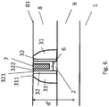
- Fig. 6 illustrates that embodiments of the present invention are also applicable in the context of non-planar devices, as for instance FINFET device or other devices wherein the active layer or region 9 protrudes from the front surface of the substrate.
- the active layer can for instance be provided as a FIN structure 9 on top of a front surface of a substrate 1.
- the dummy gate structure or final gate structure can then be provided at least partially on top of the active region, and can be provided around the protruding region (e.g. FIN structure), in a certain view "wrapping" the FIN structure, in first areas.
- the same dummy gate structure or final gate structure can be provided on the substrate 1, while extending adjacent to the FIN structure, for instance towards a further adjacent FIN structure on the substrate.
- the dummy gate structure or final gate structure can be provided on the substrate 1, while extending adjacent to the FIN structure, for instance towards a further adjacent FIN structure on the substrate.
- Embodiments of the present invention may then be even more advantageous.
- an optimal thickness is a thickness of about 5 nm.
- this optimal thickness is expected to be smaller, and can be for instance 4nm.
- an optimal thickness can be 3nm.
- the thickness of the metal layer also called metal source
- a typical combination of diffusion layer/metal layer for instance silicon layer/metal layer, has a thickness combination of 5nm/20nm.
Landscapes
- Engineering & Computer Science (AREA)
- Microelectronics & Electronic Packaging (AREA)
- Power Engineering (AREA)
- Computer Hardware Design (AREA)
- Condensed Matter Physics & Semiconductors (AREA)
- General Physics & Mathematics (AREA)
- Physics & Mathematics (AREA)
- Manufacturing & Machinery (AREA)
- Ceramic Engineering (AREA)
- Chemical & Material Sciences (AREA)
- Composite Materials (AREA)
- Materials Engineering (AREA)
- Insulated Gate Type Field-Effect Transistor (AREA)
- Electrodes Of Semiconductors (AREA)
- Metal-Oxide And Bipolar Metal-Oxide Semiconductor Integrated Circuits (AREA)
- Thin Film Transistor (AREA)
Description
- The present disclosure relates to a method for providing a gate metal layer in a transistor device. More specifically it related to a method for providing a gate metal layer in a transistor device having relatively small gate dimensions, e.g. relatively small gate width.
- A process of manufacturing a MOS semiconductor transistor can be based on a so called gate-last approach. In a gate-last approach, also referred to as replacement-gate (RMG) approach, the metal gate deposition occurs after a number of activation anneal steps (i.e. junction activation, source/drain activation) and a silicidation step. In an alternative approach, a gate-first approach, the metal gate is deposited on a high-k gate dielectric prior to the activation anneal steps, such that the metal gate is exposed to high temperatures (temperatures up to 1100 degrees Celsius or higher), which can be detrimental for the proper working of the device. In the gate-last approach, the metal of the metal gate is thus not exposed to these high temperatures.
- In the gate-last approach, a gate dielectric layer and a dummy gate electrode layer are provided and patterned on a substrate, thereby forming a dummy gate stack. Later, spacers are provided aside the dummy gate stack, and activation of the source/drain areas is performed. An additional silicidation process can be performed, which is known to the skilled person. The patterned dummy gate stack is then completely or partially removed and replaced by a final gate stack.
- In a Field Effect Transistor (FET) device, the gate requires a threshold voltage (Vt) to render the channel conductive. Complementary MOS (CMOS) processes fabricate both n-channel and p-channel (respectively NMOS and PMOS) transistors. The threshold voltage Vt is influenced by what is called the effective work function difference (ΔWFeff). effective work function differences of the respective PMOS and NMOS gate materials (gate stacks) and their corresponding channel regions are typically independently established through channel processing and gate processing. In other words, both gate dielectric (consisting i.e. of a host dielectric and possible different capping layers) and gate electrode (consisting i.e. of at least one metal layer) determine the effective work function of the gate stack (device) (WFeff). Moreover, the gate processing itself (i.e. the sequence of the different processes and/or the thermal treatments applied) may have an influence on the effective work function of the gate stack (device) (WFeff).
- In a replacement metal gate FET, TiAl is known to be an appropriate metal for controlling the threshold voltage. The TiAl metal is generally formed by Physical Vapor Deposition (PVD) or Chemical Vapor Deposition (CVD). It is though difficult if not impossible to provide the final gate stack for small gate widths (e.g. filling the gap between the spacers generated by the dummy gate structure), biasing a good control of the Vt.
- There exists a need for processes that allow a better control of these threshold voltages.
- In
US2004/0126977 A1 , a process is disclosed for producing an electronic component including covering a substrate with a portion defining, with the substrate, a volume at least partly filled with a temporary material. The temporary material is then removed via chimney for access to said volume. A deposition of a fill material is then made in said volume, the fill material being obtained from precursors supplied via the chimney. - According to the present invention, a method is provided for manufacturing a field effect transistor, the method comprising the steps of:
- providing a dummy gate structure on a substrate, the dummy gate structure comprising a gate dielectric layer and dummy gate electrode layer, the dummy gate structure being laterally defined by a gate trench defined by inner sidewalls of a set of spacers;
- laterally embedding the dummy gate structure by means of one or more embedding layers, the one or more embedding layers defining a front surface;
- removing the dummy gate electrode layer in between the inner sidewalls of the set of spacers;
- providing a continuous diffusion layer, the diffusion layer extending at least on top of the gate dielectric layer, on inner sidewalls of the set of spacers, and at least on a portion of the front surface;
- providing a metal layer comprising a metal on top of the diffusion layer, on the front surface and whereby the metal does not enter said gate trench;
- applying an anneal step, the anneal step being adapted for driving diffusion of the metal of the metal layer into the diffusion layer, and for further diffusing the metal in the diffusion layer towards the portion of the diffusion layer in the area corresponding to the area of the gate dielectric; and
- filling the area in between the inner sidewalls of the set of spacers with a final gate metal filling layer.
- The portion of the front surface can correspond to an upper surface of the set of spacers. The upper surface of the set of spacers and the front surface of the one or more embedding layers may lie in a single plane. This single plane may have been defined by a planarization process, as for instance a CMP process, performed on an intermediate structure comprising a dummy gate structure and one or more transistor embedding layers surrounding the dummy gate structure.
- The diffusion layer is continuous. It is preferably a conformal layer which follows substantially the surface of the underlying topology, and has a uniform thickness. Such a conformal layer does not substantially change the underlying topology, i.e. the shape of the underlying surface.
- According to preferred embodiments, the diffusion layer comprises silicon. It may comprise for instance polycrystalline silicon, multicrystalline silicon or monocrystalline silicon.
- According to preferred embodiments, the diffusion layer has a thickness within the range of 2 to 10 nm.
- According to preferred embodiments, the metal layer comprises Aluminum, Indium, Gallium or Nickel.
- According to preferred embodiments, the anneal step is performed at a temperature in between 400°C and 600°C.
- According to preferred embodiments, the anneal step has a duration of 1 to 10 minutes.
- According to preferred embodiments, the vertical distance between the metal layer in an area corresponding to the upper surface of the set of spacers and the upper surface of the diffusion layer in an area on top of the gate dielectric layer is smaller than 170nm. This is advantageous as it reduces the time period for successfully driving diffusion of the metal into the diffusion layer, and for further diffusing the metal in the diffusion layer towards the portion of the diffusion layer in the area corresponding to the area of the gate dielectric.
- According to preferred embodiments, the vertical distance between the metal layer in an area corresponding to the upper surface of the set of spacers and the upper surface of the diffusion layer in an area on top of the gate dielectric layer is larger than 60nm. It will be appreciated to the skilled person that methods according to aspects of the present invention can be applied for a relatively large vertical distance between the metal layer in an area corresponding to the upper surface of the set of spacers and the upper surface of the diffusion layer in an area on top of the gate dielectric layer.
- According to preferred embodiments, the diffusion layer is deposited by means of Chemical Vapor Deposition (CVD).
- According to preferred embodiments, the anneal step is such that the diffusion layer and the metal layer merge completely into a single merged layer of mixed constitution, in other words into a single merged layer which is homogeneous, i.e. with constant constitution.
- According to preferred embodiments, the method further comprises performing a Chemical Mechanical Polishing (CMP) step after applying the anneal step and filling the area in between the inner sidewalls of the set of spacers with a final gate metal filling layer.
- According to preferred embodiments, the field effect transistor is of the non-planar type comprising at least one FIN structure protruding from a front surface of the substrate, and wherein the dummy gate structure is provided at least partially on the FIN structure and at least partially adjacent to the FIN structure.
- According to preferred embodiments, the gate electrode layer has a thickness between 5 to 20 nm.
- According to preferred embodiments, the gate electrode layer comprises SiAl, Siln, SiGa or SiNi.
- The disclosure will be further elucidated by means of the following description and the appended figures.
-
Figures 1 to 6 illustrate a preferred embodiment of the present disclosure. - The present disclosure will be described with respect to particular embodiments and with reference to certain drawings but the disclosure is not limited thereto but only by the claims. The drawings described are only schematic and are non-limiting. In the drawings, the size of some of the elements may be exaggerated and not drawn on scale for illustrative purposes. The dimensions and the relative dimensions do not necessarily correspond to actual reductions to practice of the disclosure.
- Furthermore, the terms first, second, third and the like in the description and in the claims, are used for distinguishing between similar elements and not necessarily for describing a sequential or chronological order. The terms are interchangeable under appropriate circumstances and the embodiments of the disclosure can operate in other sequences than described or illustrated herein.
- Moreover, the terms top, bottom, over, under and the like in the description and the claims are used for descriptive purposes and not necessarily for describing relative positions. The terms so used are interchangeable under appropriate circumstances and the embodiments of the disclosure described herein can operate in other orientations than described or illustrated herein.
- Furthermore, the various embodiments, although referred to as "preferred" are to be construed as exemplary manners in which the disclosure may be implemented rather than as limiting the scope of the disclosure.
- The term "comprising", used in the claims, should not be interpreted as being restricted to the elements or steps listed thereafter; it does not exclude other elements or steps. It needs to be interpreted as specifying the presence of the stated features, integers, steps or components as referred to, but does not preclude the presence or addition of one or more other features, integers, steps or components, or groups thereof. Thus, the scope of the expression "a device comprising A and B" should not be limited to devices consisting only of components A and B, rather with respect to the present disclosure, the only enumerated components of the device are A and B, and further the claim should be interpreted as including equivalents of those components.
- In the following certain embodiments of the present invention will be described with reference to a silicon (Si) substrate but it should be understood that these embodiments apply equally well to other semiconductor substrates. In embodiments, the "substrate" may include a semiconductor substrate such as e.g. a silicon, a gallium arsenide (GaAs), a gallium arsenide phosphide (GaAsP), an indium phosphide (InP), a germanium (Ge), or a silicon germanium (SiGe) substrate. The "substrate" may include for example, an insulating layer such as a SiO2 or a Si3N4 layer in addition to a semiconductor substrate portion. Thus, the term substrate also includes silicon-on-glass, silicon-on-sapphire substrates. The term "substrate" is thus used to define generally the elements for layers that underlie a layer or portions of interest. Also, the "substrate" may be any other base on which a layer is formed, for example a glass or metal layer. Accordingly a substrate may be a wafer such as a blanket wafer or may be a layer applied to another base material, e.g. an epitaxial layer grown onto a lower layer.
-
FIG.1 illustrates asemiconductor substrate 1, e.g. a silicon substrate. The substrate may comprise multiple distinct regions. Most preferably two distinct regions may be defined in thesubstrate 1, a first region and a second region. The first region may also be referred as the first active region of the device (NMOS or PMOS region) and the second region may also be referred as the second active region of the device (PMOS or NMOS region respectively). The first region and the second region may be electrically isolated from each other by an insulating region. A possible way to isolate the first and second region from each other is by using shallow trench isolation (STI) in between. STI is typically a deep narrow trench, filled with oxide, etched into the semiconductor substrate in between adjacent devices in an integrated circuit to provide electrical isolation between. Alternatively, local oxidation of silicon (LOCOS) may be used. - For simplicity reasons only one of those regions is depicted in
Figure 1 , and also the insulating region has not been depicted. It will be appreciated that the embodiments of the present invention can be applied for both NMOS as well as PMOS transistors. - After providing the active regions a
gate dielectric layer 2 is provided on the substrate. Thedielectric layer 2 may be a layer of insulating material, such as for example silicon dioxide (SiO2), silicon nitride (SiN) or silicon oxynitride (SixOyN1-x-y) or more preferably any high-k dielectric material (i.e. k > 3.9) such as for example HfO2, TaOx, Al2Oy, or any combination made thereof. The gate dielectric layer may be formed by thermal oxidation, atomic layer deposition (ALD) or chemical vapor deposition (CVD) or physical vapor deposition (PVD), or any other suitable method known to a person skilled in the art. The gate dielectric layer may comprise a stack of dielectric materials, such as for example a high-k material (e.g. HfO2) formed on top of an (optional) interfacial dielectric layer (e.g. SiO2- not shown) between thesubstrate 1 and high-k material. - After providing the gate dielectric layer a dummy gate electrode layer is provided on the
gate dielectric layer 2. Spacers are formed. - In a further process the patterned dummy gate electrode layer is removed, resulting in a device depicted in
Fig. 1 . The removal of the patterned dummy gate electrode may be done for example by means of a wet etch process or other etch processes known by the skilled person. - Conventional process steps, materials and equipment may be used to generate a device as illustrated in
FIG. 1 , which is of the planar type, i.e. process steps comprising patterning (e.g. using conventional lithography) thegate dielectric layer 2 and the dummy gate electrode layer to form a dummy gate stack, providing one or more spacers 3 (31,32) aside of the dummy gate stack, activation of the source (S) /drain (D) regions (extension regions/junction regions) in the first region and additional silicidation. For the activation of the source/drain regions and as well for the formation of the silicide regions in the source/drain regions an annealing process is necessary. This annealing process comprises a high temperature process. This is a high thermal budget process. The temperature of the annealing process is typically higher than 500 degrees Celsius, preferably higher than 800 degrees Celsius, more preferably in the range of 800 degrees Celsius to 1200 degrees Celsius. Spike annealing or rapid thermal annealing (RTA) may be used. - The spacers 3 (31,32) preferably comprise an insulating material such as for example silicon dioxide (SiO2), silicon nitride (SiN) or silicon oxynitride (SiON). They can for instance comprise a stack structure as a for instance SiN/SiO. Spacers 3 (31,32) may be deposited by ALD or CVD and patterned by anisotropic etching, or any other suitable method known to a person skilled in the art.
- After removing the dummy gate electrode material, the underlying
gate dielectric layer 2 is exposed. The removal of the dummy gate electrode material may be done using an etching process which is selective towards the underlying gate dielectric material. More specifically, first one or more embeddinglayers 8, for instance adielectric layer 8 may be formed. The formation of the dielectric layer 8 (e.g. premetal dielectric layer) may be done for example by depositing thedielectric layer 8 using CVD, followed by polishing back to a level corresponding to afront surface dielectric layer 8 forms a protective layer for protecting the underlying source/drain regions and silicide regions andspacers 3 during the subsequent etching process for removing the dummy gate electrode material. Alternatively, a protective dielectric liner may be formed on the source/drain regions and silicide regions and aside of thespacers 3. Using a CMP-less hard mask opening process, the dummy gate electrode material may be removed. After removing the dummy gate electrode material a trench is formed (having a depth d) in the area in between thesidewall spacers 3, delimited by the upper surface of thegate dielectric 2 and the inner sidewalls of the spacer structure 3 (322). After removal of the dummy gate electrode material, thegate dielectric layer 2 is still present in the gate stack. - A final gate electrode layer is then applied in between said inner sidewalls of the set of spacers. According to preferred embodiments of the present invention, this can be achieved as follows.
- A connected,
conformal diffusion layer 4 is applied, for instance a silicon layer, the diffusion layer extending at least on top of the gate dielectric layer, on inner sidewalls of the set of spacers, and on anupper surface 811 of the set of spacers (311 and/or 321), as for instance depicted inFigure 2 . Note that in the example given thespacer structures 3 each comprise afirst spacer 31 and asecond spacer 32, which is optional. Theinner sidewall 322 of thespacer 32, but more generally thespacer structure 3, laterally defines the gate trench. - The diffusion layer can for instance comprise or consist of silicon, which can for instance be applied by a CVD process. The thickness of the
diffusion layer 4 is preferably within the range of 2 to 10 nm, as forinstance 5 nm. This CVD deposited silicon layer can be deposited at a temperature of for instance 600°C. Preferably the diffusion layer should be applicable in a substantially conformal way over the front surface of the substrate and within the gate trench, i.e. on top of thegate dielectric 2 and theinner sidewalls 322 of thespacer structures 3. - Then, a
metal layer 5 is provided comprising a metal on top of thediffusion layer 4, at least in the area corresponding to the upper surface of the set of spacers, as illustrated inFig. 3 . The metal layer can for instance be an Aluminum layer deposited by Plasma Vapor Deposition (PVD) or CVD at room temperature, and can be for instance 20 nm thick. It is useful for understanding the present invention that some metal of themetal layer 5 may thereby enter the gate trench, but according to the method of the present invention the metal does not enter the gate trench, e.g. the metal layer does not have a similar requirement of being conformal. - Then, an anneal step is applied, the anneal step being adapted for driving diffusion of the metal into the
diffusion layer 4, and for further diffusing the metal in the diffusion layer towards the portion of the diffusion layer in the area corresponding to the area of the gate dielectric. The anneal step can be such that thediffusion layer 4 and themetal layer 5 merge completely into a single merged layer ofmixed constitution 6, as illustrates inFigure 4 , for instance an alloy layer, as for instance a Silicon Aluminum alloy. Preferably, the anneal step is applied at a temperature between 450°C and 550°C, for instance at about 500°C. The anneal step can be performed in the presence of a forming gas, for instance under a N2 atmosphere. The duration of the anneal can be tuned in order to achieve the desired effect, and can depend on for instance the temperature and the distance, which can be approximated by the vertical distance, that the metal has to diffuse in order to reach the gate electrode area. The duration can for instance be between 1 and 60 minutes, forinstance 5 minutes. - The vertical distance between the metal layer in an area corresponding to the upper surface of the set of spacers (311, 321) and/or
front surface 81, and the upper surface of the diffusion layer in an area on top of the gate dielectic layer can for instance be in the range of 60 nm to 170 nm, for instance in the range of 60 nm to 120 nm. It can preferably be smaller than 170 nm, for instance when the diffusion anneal step is performed at 500°C. - The diffusion layer is preferably a silicon layer or silicon comprising layer, but other layers which can be applied in a similar way, and which would allow diffusion and/or merging into an alloy which can serve as gate electrode layer by interaction with an associated metal (layer) as explained before can be used, as will be appreciated by the skilled person.
- Finally, the remaining
open area 70 in between theinner sidewalls 322 of the set ofspacers 3 is filled with a final gatemetal filling layer 7, for instance a W, Al or Cu layer, according to state of the art techniques known to the skilled person, as illustrated inFigure 5 . For instance, a metal layer can be deposited over the front surface of the substrate, filing the gate trench but possibly covering the area next to the trench also. A CMP step can then be applied to remove the metal layer outside of the gate area, for instance to a level corresponding to the level of thefront surface 81 or upper surfaces of the spacers 3 (311, 321), or a lower level parallel to this level. Note that the layer ofmixed constitution 6 remains in the final device. - It is an advantage of embodiments of the present invention that for small gate dimensions, corresponding to small gate trench dimensions, to a gate length of less than 20nm, still a good control can be achieved of the threshold voltage of the final transistor device.
- The embodiment described above relates to manufacturing a transistor device with an active region or layer of the planar type. The upper surface of the active region or layer lies flat with the surrounding front surface of the substrate.
Fig. 6 illustrates that embodiments of the present invention are also applicable in the context of non-planar devices, as for instance FINFET device or other devices wherein the active layer orregion 9 protrudes from the front surface of the substrate. The active layer can for instance be provided as aFIN structure 9 on top of a front surface of asubstrate 1. The dummy gate structure or final gate structure can then be provided at least partially on top of the active region, and can be provided around the protruding region (e.g. FIN structure), in a certain view "wrapping" the FIN structure, in first areas. In second areas the same dummy gate structure or final gate structure can be provided on thesubstrate 1, while extending adjacent to the FIN structure, for instance towards a further adjacent FIN structure on the substrate. It will be appreciated that in the embodiments with one or more protruding active regions (e.g. FIN structures), it may even be more difficult to provide a metal electrode layer in the trench defined by the dummy gate structure, for instance in the area on the substrate adjacent to the FIN structure, because of the increase of height variations on the front surface of the intermediate substrate (represented by the arrow d' inFig. 6 , which ends at it lower end a level of the upper surface of the dielectric layer (itself not depicted) in the area adjacent to the FIN, for instance in between two adjacent, closely spaced FINs). Embodiments of the present invention may then be even more advantageous. - The following combination of process parameters has been proven to be successful:
- providing a diffusion layer of polycrystalline silicon, deposited by CVD at 600°C, having a thickness of about 5 nm;
- depositing by PVD or CVD of an aluminium layer having a thickness of about 20 nm on the diffusion layer;
- performing a thermal anneal in a N2 atmosphere, at 500°C for about 5 minutes.
- It will furthermore be appreciated that for different "technology nodes", known to the skilled person to the typical dimension of the gate length, corresponding to the horizontal distance in between the inner sidewalls of the set of spacers, different optimal thicknesses of the diffusion layer may exist. For instance, for the 20nm node and 14 nm node an optimal thickness is a thickness of about 5 nm. For the 10 nm node, this optimal thickness is expected to be smaller, and can be for instance 4nm. For the 7nm node, an optimal thickness can be 3nm. The thickness of the metal layer (also called metal source) can be about 20nm for all nodes. When generalising, a typical combination of diffusion layer/metal layer, for instance silicon layer/metal layer, has a thickness combination of 5nm/20nm.
wherein providing a final gate electrode layer comprises:
Claims (11)
- A method for manufacturing a field effect transistor, the method comprising the steps of:- providing a dummy gate structure on a substrate (1), said dummy gate structure comprising a gate dielectric layer (2) and dummy gate electrode layer, said dummy gate structure being laterally defined by a gate trench defined by inner sidewalls of a set of spacers (31,32);- laterally embedding said dummy gate structure by means of one or more embedding layers (8), said one or more embedding layers defining a front surface (81);- removing said dummy gate electrode layer in between said inner sidewalls (322) of said set of spacers (31,32);- providing a final gate electrode layer replacing said dummy gate electrode layer in between said inner sidewalls (322) of said set of spacers (31,32);wherein the horizontal distance between the inner sidewalls (322) of said spacers is smaller than 20 nm
wherein providing a final gate electrode layer comprises- providing a continuous diffusion layer (4), said diffusion layer (4) extending at least on top of said gate dielectric layer (2), on inner sidewalls of said set of spacers (31,32), and at least on a portion of said front surface (81);- providing a metal layer (5) comprising a metal on top of said diffusion layer (4), on said front surface and whereby said metal does not enter said gate trench;- applying an anneal step, said anneal step being adapted for driving diffusion of said metal of said metal layer (5) into said diffusion layer (4), and for further diffusing said metal in said diffusion layer towards the portion of said diffusion layer in the area corresponding to the area of the gate dielectric (2);- filling the area in between said inner sidewalls of said set of spacers with a final gate metal filling layer. - A method according to claim 1, wherein said diffusion layer (4) comprises silicon.
- A method according to any of the previous claims, wherein said diffusion layer (4) has a thickness within the range of 2 to 10 nm.
- A method according to any of the previous claims, wherein said metal layer (5) comprises Aluminum, Indium, Gallium or Nickel.
- A method according to any of the previous claims, wherein said anneal step is performed at a temperature in between 400°C and 600°C.
- A method according to any of the previous claims, wherein said anneal step has a duration of 1 to 10 minutes.
- A method according to any of the previous claims, wherein a vertical distance between the metal layer on the front surface and an upper surface of the diffusion layer in an area on top of the gate dielectric layer is smaller than 170nm.
- A method according to any of the previous claims, wherein said diffusion layer (4) is deposited by means of Chemical Vapor Deposition (CVD).
- A method according to any of the previous claims, wherein said anneal step is such that said diffusion layer (4) and said metal layer (5) merge completely into a single merged layer (6) of mixed constitution.
- A method according to any of the previous claims, further comprising performing a Chemical Mechanical Polishing (CMP) step after applying said anneal step and filling the area in between said inner sidewalls (322) of said set of spacers with a final gate metal filling layer.
- A method according to any of the previous claims, wherein said field effect transistor is of the non-planar type comprising at least one FIN structure protruding from a front surface of said substrate, and wherein said dummy gate structure is provided at least partially on said FIN structure and at least partially adjacent to said FIN structure.
Priority Applications (3)
| Application Number | Priority Date | Filing Date | Title |
|---|---|---|---|
| EP13166902.0A EP2802003B1 (en) | 2013-05-07 | 2013-05-07 | Method for providing a gate metal layer of a transistor device |
| JP2014086568A JP6158132B2 (en) | 2013-05-07 | 2014-04-18 | Method of providing a gate metal layer of a transistor device and associated transistor |
| US14/271,956 US9202695B2 (en) | 2013-05-07 | 2014-05-07 | Method for providing a gate metal layer of a transistor device and associated transistor |
Applications Claiming Priority (1)
| Application Number | Priority Date | Filing Date | Title |
|---|---|---|---|
| EP13166902.0A EP2802003B1 (en) | 2013-05-07 | 2013-05-07 | Method for providing a gate metal layer of a transistor device |
Publications (2)
| Publication Number | Publication Date |
|---|---|
| EP2802003A1 EP2802003A1 (en) | 2014-11-12 |
| EP2802003B1 true EP2802003B1 (en) | 2019-08-28 |
Family
ID=48227076
Family Applications (1)
| Application Number | Title | Priority Date | Filing Date |
|---|---|---|---|
| EP13166902.0A Active EP2802003B1 (en) | 2013-05-07 | 2013-05-07 | Method for providing a gate metal layer of a transistor device |
Country Status (3)
| Country | Link |
|---|---|
| US (1) | US9202695B2 (en) |
| EP (1) | EP2802003B1 (en) |
| JP (1) | JP6158132B2 (en) |
Families Citing this family (5)
| Publication number | Priority date | Publication date | Assignee | Title |
|---|---|---|---|---|
| US10437153B2 (en) | 2014-10-23 | 2019-10-08 | SCREEN Holdings Co., Ltd. | Heat treatment method and heat treatment apparatus |
| CN108962892B (en) * | 2017-05-26 | 2021-02-26 | 联华电子股份有限公司 | Semiconductor element and manufacturing method thereof |
| US10204828B1 (en) | 2018-02-09 | 2019-02-12 | International Business Machines Corporation | Enabling low resistance gates and contacts integrated with bilayer dielectrics |
| US10529823B2 (en) | 2018-05-29 | 2020-01-07 | International Business Machines Corporation | Method of manufacturing a semiconductor device having a metal gate with different lateral widths between spacers |
| US11978774B2 (en) * | 2020-10-05 | 2024-05-07 | Sandisk Technologies Llc | High voltage field effect transistor with vertical current paths and method of making the same |
Family Cites Families (12)
| Publication number | Priority date | Publication date | Assignee | Title |
|---|---|---|---|---|
| JPH08255766A (en) * | 1995-03-17 | 1996-10-01 | Sony Corp | Manufacture of semiconductor device |
| JP2002299610A (en) * | 2001-03-30 | 2002-10-11 | Toshiba Corp | Semiconductor device and method of manufacturing the same |
| FR2844396B1 (en) * | 2002-09-06 | 2006-02-03 | St Microelectronics Sa | METHOD FOR PRODUCING AN INTEGRATED ELECTRONIC COMPONENT AND ELECTRICAL DEVICE INCORPORATING AN INTEGRATED COMPONENT THUS OBTAINED |
| US7071086B2 (en) * | 2003-04-23 | 2006-07-04 | Advanced Micro Devices, Inc. | Method of forming a metal gate structure with tuning of work function by silicon incorporation |
| US7268065B2 (en) * | 2004-06-18 | 2007-09-11 | Taiwan Semiconductor Manufacturing Company, Ltd. | Methods of manufacturing metal-silicide features |
| US7091118B1 (en) | 2004-11-16 | 2006-08-15 | Advanced Micro Devices, Inc. | Replacement metal gate transistor with metal-rich silicon layer and method for making the same |
| US8294202B2 (en) * | 2009-07-08 | 2012-10-23 | Taiwan Semiconductor Manufacturing Company, Ltd. | Metal gate structure of a semiconductor device |
| US8304841B2 (en) * | 2009-09-14 | 2012-11-06 | Taiwan Semiconductor Manufacturing Company, Ltd. | Metal gate transistor, integrated circuits, systems, and fabrication methods thereof |
| JP5598145B2 (en) * | 2010-08-04 | 2014-10-01 | 富士通セミコンダクター株式会社 | Semiconductor device manufacturing method and semiconductor device |
| US8492286B2 (en) | 2010-11-22 | 2013-07-23 | International Business Machines Corporation | Method of forming E-fuse in replacement metal gate manufacturing process |
| US8450169B2 (en) | 2010-11-29 | 2013-05-28 | International Business Machines Corporation | Replacement metal gate structures providing independent control on work function and gate leakage current |
| US20120135590A1 (en) | 2010-11-30 | 2012-05-31 | Advanced Technology Materials, Inc. | Silicon removal from surfaces and method of forming high k metal gate structures using same |
-
2013
- 2013-05-07 EP EP13166902.0A patent/EP2802003B1/en active Active
-
2014
- 2014-04-18 JP JP2014086568A patent/JP6158132B2/en active Active
- 2014-05-07 US US14/271,956 patent/US9202695B2/en active Active
Non-Patent Citations (1)
| Title |
|---|
| None * |
Also Published As
| Publication number | Publication date |
|---|---|
| JP6158132B2 (en) | 2017-07-05 |
| EP2802003A1 (en) | 2014-11-12 |
| JP2014220496A (en) | 2014-11-20 |
| US20140332864A1 (en) | 2014-11-13 |
| US9202695B2 (en) | 2015-12-01 |
Similar Documents
| Publication | Publication Date | Title |
|---|---|---|
| US9391075B2 (en) | Integrated circuit and method for fabricating the same having a replacement gate structure | |
| US9287273B2 (en) | Method for manufacturing a semiconductor device comprising transistors each having a different effective work function | |
| US10872893B2 (en) | Dual nitride stressor for semiconductor device and method of manufacturing | |
| US9698058B2 (en) | Structure and method for FinFET device | |
| TWI596675B (en) | Finfet channel on oxide structures and related methods | |
| US9231067B2 (en) | Semiconductor device and fabricating method thereof | |
| US9034716B2 (en) | Method of making a FinFET device | |
| CN109585373B (en) | FINFET structure with controllable air gap | |
| TWI604516B (en) | Semiconductor device and method for manufacturing the same | |
| CN107275210B (en) | Semiconductor element and manufacturing method thereof | |
| US10276574B2 (en) | Semiconductor device and manufacturing method thereof | |
| KR101808919B1 (en) | Method for manufacturing finfet with doped isolation insulating layer | |
| US20130043517A1 (en) | Semiconductor Structure And Method For Manufacturing The Same | |
| US9257558B2 (en) | FinFET device with gate oxide layer | |
| TW201822263A (en) | Semiconductor device and method for fabricating the same | |
| CN104916542A (en) | Structure and method for semiconductor device | |
| US20150221768A1 (en) | Semiconductor structure and method for manufacturing the same | |
| US9202695B2 (en) | Method for providing a gate metal layer of a transistor device and associated transistor | |
| KR102277762B1 (en) | Semiconductor device and method of manufacture | |
| TW201543679A (en) | Semiconductor device structure and method for forming the same | |
| US20210013205A1 (en) | Semiconductor device and manufacturing method thereof | |
| TWI814888B (en) | Method for fabricating semiconductor device | |
| CN114121660B (en) | Semiconductor element and manufacturing method thereof | |
| CN116504828A (en) | Semiconductor device with a semiconductor element having a plurality of electrodes | |
| CN104952797B (en) | A kind of preparation method of semiconductor devices |
Legal Events
| Date | Code | Title | Description |
|---|---|---|---|
| PUAI | Public reference made under article 153(3) epc to a published international application that has entered the european phase |
Free format text: ORIGINAL CODE: 0009012 |
|
| 17P | Request for examination filed |
Effective date: 20130507 |
|
| AK | Designated contracting states |
Kind code of ref document: A1 Designated state(s): AL AT BE BG CH CY CZ DE DK EE ES FI FR GB GR HR HU IE IS IT LI LT LU LV MC MK MT NL NO PL PT RO RS SE SI SK SM TR |
|
| AX | Request for extension of the european patent |
Extension state: BA ME |
|
| R17P | Request for examination filed (corrected) |
Effective date: 20150423 |
|
| RBV | Designated contracting states (corrected) |
Designated state(s): AL AT BE BG CH CY CZ DE DK EE ES FI FR GB GR HR HU IE IS IT LI LT LU LV MC MK MT NL NO PL PT RO RS SE SI SK SM TR |
|
| STAA | Information on the status of an ep patent application or granted ep patent |
Free format text: STATUS: EXAMINATION IS IN PROGRESS |
|
| 17Q | First examination report despatched |
Effective date: 20171109 |
|
| RAP1 | Party data changed (applicant data changed or rights of an application transferred) |
Owner name: IMEC VZW |
|
| GRAP | Despatch of communication of intention to grant a patent |
Free format text: ORIGINAL CODE: EPIDOSNIGR1 |
|
| STAA | Information on the status of an ep patent application or granted ep patent |
Free format text: STATUS: GRANT OF PATENT IS INTENDED |
|
| INTG | Intention to grant announced |
Effective date: 20190425 |
|
| GRAS | Grant fee paid |
Free format text: ORIGINAL CODE: EPIDOSNIGR3 |
|
| GRAA | (expected) grant |
Free format text: ORIGINAL CODE: 0009210 |
|
| STAA | Information on the status of an ep patent application or granted ep patent |
Free format text: STATUS: THE PATENT HAS BEEN GRANTED |
|
| AK | Designated contracting states |
Kind code of ref document: B1 Designated state(s): AL AT BE BG CH CY CZ DE DK EE ES FI FR GB GR HR HU IE IS IT LI LT LU LV MC MK MT NL NO PL PT RO RS SE SI SK SM TR |
|
| REG | Reference to a national code |
Ref country code: GB Ref legal event code: FG4D |
|
| REG | Reference to a national code |
Ref country code: CH Ref legal event code: EP |
|
| REG | Reference to a national code |
Ref country code: AT Ref legal event code: REF Ref document number: 1173448 Country of ref document: AT Kind code of ref document: T Effective date: 20190915 |
|
| REG | Reference to a national code |
Ref country code: IE Ref legal event code: FG4D |
|
| REG | Reference to a national code |
Ref country code: DE Ref legal event code: R096 Ref document number: 602013059654 Country of ref document: DE |
|
| REG | Reference to a national code |
Ref country code: NL Ref legal event code: MP Effective date: 20190828 |
|
| REG | Reference to a national code |
Ref country code: LT Ref legal event code: MG4D |
|
| PG25 | Lapsed in a contracting state [announced via postgrant information from national office to epo] |
Ref country code: SE Free format text: LAPSE BECAUSE OF FAILURE TO SUBMIT A TRANSLATION OF THE DESCRIPTION OR TO PAY THE FEE WITHIN THE PRESCRIBED TIME-LIMIT Effective date: 20190828 Ref country code: HR Free format text: LAPSE BECAUSE OF FAILURE TO SUBMIT A TRANSLATION OF THE DESCRIPTION OR TO PAY THE FEE WITHIN THE PRESCRIBED TIME-LIMIT Effective date: 20190828 Ref country code: PT Free format text: LAPSE BECAUSE OF FAILURE TO SUBMIT A TRANSLATION OF THE DESCRIPTION OR TO PAY THE FEE WITHIN THE PRESCRIBED TIME-LIMIT Effective date: 20191230 Ref country code: NL Free format text: LAPSE BECAUSE OF FAILURE TO SUBMIT A TRANSLATION OF THE DESCRIPTION OR TO PAY THE FEE WITHIN THE PRESCRIBED TIME-LIMIT Effective date: 20190828 Ref country code: FI Free format text: LAPSE BECAUSE OF FAILURE TO SUBMIT A TRANSLATION OF THE DESCRIPTION OR TO PAY THE FEE WITHIN THE PRESCRIBED TIME-LIMIT Effective date: 20190828 Ref country code: LT Free format text: LAPSE BECAUSE OF FAILURE TO SUBMIT A TRANSLATION OF THE DESCRIPTION OR TO PAY THE FEE WITHIN THE PRESCRIBED TIME-LIMIT Effective date: 20190828 Ref country code: BG Free format text: LAPSE BECAUSE OF FAILURE TO SUBMIT A TRANSLATION OF THE DESCRIPTION OR TO PAY THE FEE WITHIN THE PRESCRIBED TIME-LIMIT Effective date: 20191128 Ref country code: NO Free format text: LAPSE BECAUSE OF FAILURE TO SUBMIT A TRANSLATION OF THE DESCRIPTION OR TO PAY THE FEE WITHIN THE PRESCRIBED TIME-LIMIT Effective date: 20191128 |
|
| PG25 | Lapsed in a contracting state [announced via postgrant information from national office to epo] |
Ref country code: AL Free format text: LAPSE BECAUSE OF FAILURE TO SUBMIT A TRANSLATION OF THE DESCRIPTION OR TO PAY THE FEE WITHIN THE PRESCRIBED TIME-LIMIT Effective date: 20190828 Ref country code: ES Free format text: LAPSE BECAUSE OF FAILURE TO SUBMIT A TRANSLATION OF THE DESCRIPTION OR TO PAY THE FEE WITHIN THE PRESCRIBED TIME-LIMIT Effective date: 20190828 Ref country code: RS Free format text: LAPSE BECAUSE OF FAILURE TO SUBMIT A TRANSLATION OF THE DESCRIPTION OR TO PAY THE FEE WITHIN THE PRESCRIBED TIME-LIMIT Effective date: 20190828 Ref country code: IS Free format text: LAPSE BECAUSE OF FAILURE TO SUBMIT A TRANSLATION OF THE DESCRIPTION OR TO PAY THE FEE WITHIN THE PRESCRIBED TIME-LIMIT Effective date: 20191228 Ref country code: LV Free format text: LAPSE BECAUSE OF FAILURE TO SUBMIT A TRANSLATION OF THE DESCRIPTION OR TO PAY THE FEE WITHIN THE PRESCRIBED TIME-LIMIT Effective date: 20190828 Ref country code: GR Free format text: LAPSE BECAUSE OF FAILURE TO SUBMIT A TRANSLATION OF THE DESCRIPTION OR TO PAY THE FEE WITHIN THE PRESCRIBED TIME-LIMIT Effective date: 20191129 |
|
| REG | Reference to a national code |
Ref country code: AT Ref legal event code: MK05 Ref document number: 1173448 Country of ref document: AT Kind code of ref document: T Effective date: 20190828 |
|
| PG25 | Lapsed in a contracting state [announced via postgrant information from national office to epo] |
Ref country code: TR Free format text: LAPSE BECAUSE OF FAILURE TO SUBMIT A TRANSLATION OF THE DESCRIPTION OR TO PAY THE FEE WITHIN THE PRESCRIBED TIME-LIMIT Effective date: 20190828 |
|
| PG25 | Lapsed in a contracting state [announced via postgrant information from national office to epo] |
Ref country code: RO Free format text: LAPSE BECAUSE OF FAILURE TO SUBMIT A TRANSLATION OF THE DESCRIPTION OR TO PAY THE FEE WITHIN THE PRESCRIBED TIME-LIMIT Effective date: 20190828 Ref country code: IT Free format text: LAPSE BECAUSE OF FAILURE TO SUBMIT A TRANSLATION OF THE DESCRIPTION OR TO PAY THE FEE WITHIN THE PRESCRIBED TIME-LIMIT Effective date: 20190828 Ref country code: DK Free format text: LAPSE BECAUSE OF FAILURE TO SUBMIT A TRANSLATION OF THE DESCRIPTION OR TO PAY THE FEE WITHIN THE PRESCRIBED TIME-LIMIT Effective date: 20190828 Ref country code: EE Free format text: LAPSE BECAUSE OF FAILURE TO SUBMIT A TRANSLATION OF THE DESCRIPTION OR TO PAY THE FEE WITHIN THE PRESCRIBED TIME-LIMIT Effective date: 20190828 Ref country code: PL Free format text: LAPSE BECAUSE OF FAILURE TO SUBMIT A TRANSLATION OF THE DESCRIPTION OR TO PAY THE FEE WITHIN THE PRESCRIBED TIME-LIMIT Effective date: 20190828 Ref country code: AT Free format text: LAPSE BECAUSE OF FAILURE TO SUBMIT A TRANSLATION OF THE DESCRIPTION OR TO PAY THE FEE WITHIN THE PRESCRIBED TIME-LIMIT Effective date: 20190828 |
|
| PG25 | Lapsed in a contracting state [announced via postgrant information from national office to epo] |
Ref country code: CZ Free format text: LAPSE BECAUSE OF FAILURE TO SUBMIT A TRANSLATION OF THE DESCRIPTION OR TO PAY THE FEE WITHIN THE PRESCRIBED TIME-LIMIT Effective date: 20190828 Ref country code: SK Free format text: LAPSE BECAUSE OF FAILURE TO SUBMIT A TRANSLATION OF THE DESCRIPTION OR TO PAY THE FEE WITHIN THE PRESCRIBED TIME-LIMIT Effective date: 20190828 Ref country code: IS Free format text: LAPSE BECAUSE OF FAILURE TO SUBMIT A TRANSLATION OF THE DESCRIPTION OR TO PAY THE FEE WITHIN THE PRESCRIBED TIME-LIMIT Effective date: 20200224 Ref country code: SM Free format text: LAPSE BECAUSE OF FAILURE TO SUBMIT A TRANSLATION OF THE DESCRIPTION OR TO PAY THE FEE WITHIN THE PRESCRIBED TIME-LIMIT Effective date: 20190828 |
|
| REG | Reference to a national code |
Ref country code: DE Ref legal event code: R097 Ref document number: 602013059654 Country of ref document: DE |
|
| PLBE | No opposition filed within time limit |
Free format text: ORIGINAL CODE: 0009261 |
|
| STAA | Information on the status of an ep patent application or granted ep patent |
Free format text: STATUS: NO OPPOSITION FILED WITHIN TIME LIMIT |
|
| PG2D | Information on lapse in contracting state deleted |
Ref country code: IS |
|
| 26N | No opposition filed |
Effective date: 20200603 |
|
| PG25 | Lapsed in a contracting state [announced via postgrant information from national office to epo] |
Ref country code: SI Free format text: LAPSE BECAUSE OF FAILURE TO SUBMIT A TRANSLATION OF THE DESCRIPTION OR TO PAY THE FEE WITHIN THE PRESCRIBED TIME-LIMIT Effective date: 20190828 |
|
| PG25 | Lapsed in a contracting state [announced via postgrant information from national office to epo] |
Ref country code: MC Free format text: LAPSE BECAUSE OF FAILURE TO SUBMIT A TRANSLATION OF THE DESCRIPTION OR TO PAY THE FEE WITHIN THE PRESCRIBED TIME-LIMIT Effective date: 20190828 Ref country code: LI Free format text: LAPSE BECAUSE OF NON-PAYMENT OF DUE FEES Effective date: 20200531 Ref country code: CH Free format text: LAPSE BECAUSE OF NON-PAYMENT OF DUE FEES Effective date: 20200531 |
|
| REG | Reference to a national code |
Ref country code: BE Ref legal event code: MM Effective date: 20200531 |
|
| GBPC | Gb: european patent ceased through non-payment of renewal fee |
Effective date: 20200507 |
|
| PG25 | Lapsed in a contracting state [announced via postgrant information from national office to epo] |
Ref country code: LU Free format text: LAPSE BECAUSE OF NON-PAYMENT OF DUE FEES Effective date: 20200507 |
|
| PG25 | Lapsed in a contracting state [announced via postgrant information from national office to epo] |
Ref country code: GB Free format text: LAPSE BECAUSE OF NON-PAYMENT OF DUE FEES Effective date: 20200507 Ref country code: IE Free format text: LAPSE BECAUSE OF NON-PAYMENT OF DUE FEES Effective date: 20200507 |
|
| PG25 | Lapsed in a contracting state [announced via postgrant information from national office to epo] |
Ref country code: BE Free format text: LAPSE BECAUSE OF NON-PAYMENT OF DUE FEES Effective date: 20200531 |
|
| PG25 | Lapsed in a contracting state [announced via postgrant information from national office to epo] |
Ref country code: MT Free format text: LAPSE BECAUSE OF FAILURE TO SUBMIT A TRANSLATION OF THE DESCRIPTION OR TO PAY THE FEE WITHIN THE PRESCRIBED TIME-LIMIT Effective date: 20190828 Ref country code: CY Free format text: LAPSE BECAUSE OF FAILURE TO SUBMIT A TRANSLATION OF THE DESCRIPTION OR TO PAY THE FEE WITHIN THE PRESCRIBED TIME-LIMIT Effective date: 20190828 |
|
| PG25 | Lapsed in a contracting state [announced via postgrant information from national office to epo] |
Ref country code: MK Free format text: LAPSE BECAUSE OF FAILURE TO SUBMIT A TRANSLATION OF THE DESCRIPTION OR TO PAY THE FEE WITHIN THE PRESCRIBED TIME-LIMIT Effective date: 20190828 |
|
| P01 | Opt-out of the competence of the unified patent court (upc) registered |
Effective date: 20230513 |
|
| PGFP | Annual fee paid to national office [announced via postgrant information from national office to epo] |
Ref country code: FR Payment date: 20230420 Year of fee payment: 11 Ref country code: DE Payment date: 20230419 Year of fee payment: 11 |