EP2777156B1 - Oscillator based frequency locked loop - Google Patents
Oscillator based frequency locked loop Download PDFInfo
- Publication number
- EP2777156B1 EP2777156B1 EP12798922.6A EP12798922A EP2777156B1 EP 2777156 B1 EP2777156 B1 EP 2777156B1 EP 12798922 A EP12798922 A EP 12798922A EP 2777156 B1 EP2777156 B1 EP 2777156B1
- Authority
- EP
- European Patent Office
- Prior art keywords
- time period
- controlled oscillator
- clock
- digitally controlled
- control setting
- Prior art date
- Legal status (The legal status is an assumption and is not a legal conclusion. Google has not performed a legal analysis and makes no representation as to the accuracy of the status listed.)
- Active
Links
- 230000010355 oscillation Effects 0.000 claims description 61
- 238000012360 testing method Methods 0.000 claims description 22
- 238000000034 method Methods 0.000 claims description 15
- 238000012545 processing Methods 0.000 claims description 8
- 230000007704 transition Effects 0.000 description 38
- 230000004044 response Effects 0.000 description 20
- 230000000630 rising effect Effects 0.000 description 8
- 238000010586 diagram Methods 0.000 description 7
- 230000001360 synchronised effect Effects 0.000 description 7
- 230000007423 decrease Effects 0.000 description 6
- 238000013461 design Methods 0.000 description 5
- 230000008859 change Effects 0.000 description 4
- 238000004891 communication Methods 0.000 description 4
- 230000008901 benefit Effects 0.000 description 2
- 230000008569 process Effects 0.000 description 2
- 230000001413 cellular effect Effects 0.000 description 1
- 238000005516 engineering process Methods 0.000 description 1
- 238000004519 manufacturing process Methods 0.000 description 1
- 238000012986 modification Methods 0.000 description 1
- 230000004048 modification Effects 0.000 description 1
- 230000000644 propagated effect Effects 0.000 description 1
- 238000012552 review Methods 0.000 description 1
- 230000001052 transient effect Effects 0.000 description 1
- 239000002699 waste material Substances 0.000 description 1
Images


Classifications
-
- H—ELECTRICITY
- H03—ELECTRONIC CIRCUITRY
- H03L—AUTOMATIC CONTROL, STARTING, SYNCHRONISATION OR STABILISATION OF GENERATORS OF ELECTRONIC OSCILLATIONS OR PULSES
- H03L7/00—Automatic control of frequency or phase; Synchronisation
-
- H—ELECTRICITY
- H03—ELECTRONIC CIRCUITRY
- H03L—AUTOMATIC CONTROL, STARTING, SYNCHRONISATION OR STABILISATION OF GENERATORS OF ELECTRONIC OSCILLATIONS OR PULSES
- H03L7/00—Automatic control of frequency or phase; Synchronisation
- H03L7/06—Automatic control of frequency or phase; Synchronisation using a reference signal applied to a frequency- or phase-locked loop
- H03L7/08—Details of the phase-locked loop
- H03L7/099—Details of the phase-locked loop concerning mainly the controlled oscillator of the loop
- H03L7/0995—Details of the phase-locked loop concerning mainly the controlled oscillator of the loop the oscillator comprising a ring oscillator
-
- G—PHYSICS
- G06—COMPUTING; CALCULATING OR COUNTING
- G06F—ELECTRIC DIGITAL DATA PROCESSING
- G06F1/00—Details not covered by groups G06F3/00 - G06F13/00 and G06F21/00
- G06F1/04—Generating or distributing clock signals or signals derived directly therefrom
- G06F1/10—Distribution of clock signals, e.g. skew
-
- H—ELECTRICITY
- H03—ELECTRONIC CIRCUITRY
- H03L—AUTOMATIC CONTROL, STARTING, SYNCHRONISATION OR STABILISATION OF GENERATORS OF ELECTRONIC OSCILLATIONS OR PULSES
- H03L7/00—Automatic control of frequency or phase; Synchronisation
- H03L7/06—Automatic control of frequency or phase; Synchronisation using a reference signal applied to a frequency- or phase-locked loop
- H03L7/16—Indirect frequency synthesis, i.e. generating a desired one of a number of predetermined frequencies using a frequency- or phase-locked loop
-
- H—ELECTRICITY
- H03—ELECTRONIC CIRCUITRY
- H03L—AUTOMATIC CONTROL, STARTING, SYNCHRONISATION OR STABILISATION OF GENERATORS OF ELECTRONIC OSCILLATIONS OR PULSES
- H03L2207/00—Indexing scheme relating to automatic control of frequency or phase and to synchronisation
- H03L2207/06—Phase locked loops with a controlled oscillator having at least two frequency control terminals
Definitions
- the present disclosure is generally related to clock generation.
- wireless computing devices such as portable wireless telephones, personal digital assistants (PDAs), and paging devices that are small, lightweight, and easily carried by users.
- portable wireless telephones such as cellular telephones and internet protocol (IP) telephones
- IP internet protocol
- wireless telephones can communicate voice and data packets over wireless networks.
- many such wireless telephones include other types of devices that are incorporated therein.
- a wireless telephone can also include a digital still camera, a digital video camera, a digital recorder, and an audio file player.
- such wireless telephones can process executable instructions, including software applications such as a web browser application, that can be used to access the Internet.
- these wireless telephones can include significant computing capabilities.
- These wireless telephones may also include various clock sources to provide clocks to the devices incorporated therein.
- a device may include a clock with a particular frequency and quality.
- a clock that has a relatively low frequency and a relatively high jitter may be used in some devices while a clock with a higher frequency and low jitter may be used in other devices.
- a digital signal processor inside a mobile phone may operate using a relatively low frequency (e.g., 100 MHz) and high jitter clock to perform some tasks, such as playing an MP3 song.
- designs with asynchronous interfaces may adequately operate using a high jitter clock.
- Use of a phase locked loop (PLL) circuit in designs and applications that may operate using low frequency and high jitter clocks may waste power.
- a PLL may take up a large area in a device and may also involve use of a power supply that is separate from a power supply for other components of the device.
- US2002145474 (A1 ) discloses a digitally controlled oscillator including an adjustable signal generating circuit adapted to generate an oscillation signal.
- a feedback loop receives the oscillation signal from the adjustable signal generating circuit.
- the feedback loop detects error in the oscillation signal and produces an error signal based on the error.
- the control logic circuit receives the error signal from the feedback loop and maintains the oscillation signal within a predetermined error range.
- a state device that is connected to the adjustable signal generating circuit maintains a previous operating state of the adjustable signal generating circuit when the digitally controlled oscillator is temporarily powered down.;
- the control logic starts the adjustable signal generating circuit at the previous operating state based upon data maintained within the state device, and restarts the feedback loop and error processing circuits in a way to avoid oscillator adjustments based on old data.
- EP1152536 (A1 ) discloses a system and method for maintaining lock of a phase locked loop within an integrated circuit during both a normal operation mode and a test mode, and during switching from the normal operation mode to the test mode.
- the method includes closing a phase locked loop feedback path of the phase locked loop with a real clock signal from a real clock tree during the normal operation mode.
- the real clock tree is selectively halted, thereby transitioning from the normal operation mode to the test mode.
- the phase locked loop feedback path of the phase locked loop is closed with a copy of a clock signal from a copy clock tree such that the phase locked loop maintains lock.;
- the steps of halting the real clock and closing the phase locked loop feedback path with a copy clock signal are completed during a single clock cycle such that lock is maintained during switching from the normal operation to the test mode.
- a frequency-locked loop may generate a relatively low frequency output clock.
- the output clock may have a frequency that is a multiple of an input clock frequency.
- the FLL may generate a 100 MHz output clock that has a relatively high jitter based on a 10 MHz input clock.
- the FLL may use a digitally controlled oscillator (DCO) to generate the output clock.
- DCO digitally controlled oscillator
- the FLL may determine whether the output clock is within a tolerance range of a target frequency based on a number of output clock cycles generated during one or more clock periods of an input clock.
- the FLL may also indicate a locked condition when the frequency of the output clock is within a tolerance range of a target frequency.
- a device in a particular embodiment, includes an oscillator and logic to selectively stop oscillation of the oscillator after a time period.
- the oscillator is configured to remain in an active mode after the time period.
- the apparatus also includes control logic that determines a control setting and selectively applies the control setting to the oscillator.
- a method in another particular embodiment, includes determining a control setting and selectively stopping oscillation of an oscillator after a time period.
- the oscillator is configured to remain in an active mode after the time period.
- the method further includes applying the control setting to the oscillator.
- an apparatus in another particular embodiment, includes means for determining a control setting and means for selectively stopping oscillation of an oscillator after a time period.
- the oscillator is configured to remain in an active mode after the time period.
- the apparatus further includes means for applying the control setting to the oscillator.
- a non-transitory computer-readable medium includes program code that, when executed by a processor, causes the processor to determine a control setting and selectively stop oscillation of an oscillator after a time period.
- the oscillator is configured to remain in an active mode after the time period.
- the program code further causes the processor to apply the control setting to the oscillator.
- One particular advantage provided by at least one of the disclosed embodiments is generation of a clock suitable for devices that operate at a relatively low clock frequency and that tolerate a relatively high jitter clock.
- a device that generates a low frequency and relatively high jitter clock may take up smaller design area and consume less power than a phased-locked-loop (PLL) circuit.
- the device may be designed using digital logic gates, which may enable sharing of a power supply with other devices. Further, a device that has a fully digital design may enable use of automatic test generation pattern tools to perform production testing.
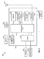
- the device 100 may be configured to generate a relatively low frequency clock.
- the device 100 includes control logic 102, a digitally controlled oscillator (DCO) 104, and stoppage logic 106.
- the control logic 102 may be coupled to the DCO 104.
- the stoppage logic 106 may be coupled to the DCO 104.
- the DCO 104 may be configured to receive a control setting 108 from the control logic 102 and to provide an output clock 114 to the control logic 102.
- the DCO 104 may be further configured to receive an enable 110 from the stoppage logic 106.
- control logic 102 may be configured to receive an input clock 112 and the output clock 114 and to generate the control setting 108.
- the control logic 102 may determine the control setting 108 and may selectively apply the control setting 108 to the DCO 104.
- the control setting 108 may be an initial control setting or a modified control setting.
- the control logic 102 may be configured to apply an initial control setting to the DCO 104 during a time period.
- the time period may be at least one clock period of the output clock 114 of the DCO 104.
- the control logic 102 may be further configured to determine a modified control setting during the time period.
- the control logic 102 may apply the modified control setting during a second time period after the time period.
- control logic 102 may apply the modified control setting 108 on a falling edge of the output clock 114.
- the time period and the second time period may be temporally contiguous.
- control setting may be an analog voltage.
- control setting may be an analog current.
- the control logic 102 may be configured to adjust the control setting 108 based on a frequency of the output clock 114. For example, the control logic 102 may increment or increase a value of the control setting 108 in response to determining that a frequency of the output clock 114 is below a desired frequency. Similarly, the control logic 104 may decrement or decrease a value of the control setting 108 in response to determining that a frequency of the output clock 114 exceeds a desired frequency. Alternatively, the control logic 102 may increment or increase a value of the control setting 108 in response to determining that a frequency of the output clock 114 exceeds a desired frequency.
- control logic 102 may decrement or decrease a value of the control setting 108 to increase a frequency of the output clock 114 in response to determining that the frequency of the output clock 114 is below a desired frequency.
- control logic 102 may determine the control setting 108 based on a number of cycles of the output clock 114 during one or more clock periods of the input clock 112.
- the DCO 104 may be configured to generate the output clock 114 based on oscillation of the DCO 104.
- a frequency of the output clock 114 may be adjusted in response to the control setting 108.
- the output clock 114 may have a first frequency value based on a first value of the control setting 108 and may have a second frequency value based on a second value of the control setting 108.
- the DCO 104 may increase a frequency of the output clock 114 in response to an incremented value of the control setting 108.
- the DCO 104 may decrease a frequency of the output clock 114 in response to a decremented value of the control setting 108.
- the DCO 104 may increase a frequency of the output clock 114 in response to a decremented value of the control setting 108. Similarly, the DCO 104 may decrease a frequency of the output clock 114 in response to an incremented value of the control setting 108.
- a frequency of the output clock 114 may be approximately a multiple of a frequency of an input clock 112.
- a frequency of the output clock 114 may approximately equal an integer multiple of a frequency of the input clock 112.
- the frequency of the output clock 114 may be a particular percentage (e.g., 6.25%) higher or lower than an integer multiple of a frequency of the input clock 112.
- a frequency of the output clock 114 may be approximately equal a non-integer multiple of a frequency of the input clock 112.
- the frequency of the output clock 114 may be a particular percentage (e.g., 6.5%) higher or lower than a non- integer multiple of the frequency of the input clock 112.
- the stoppage logic 106 may be configured to generate an enable signal 110 that is provided to the DCO 104.
- the stoppage logic 106 may selectively stop oscillation of the DCO 104 after a time period.
- the time period may correspond to a period between a start or a restart of oscillation of the DCO 104 and a last active edge (e.g., a rising edge) of the output clock 114 before the enable signal 110 toggles to a value that may stop oscillation of the DCO 104.
- the stoppage logic 106 may stop oscillation of the DCO 104 by changing the enable 110 from a first value that enables oscillation of the DCO 104 to a second value that stops oscillation of the DCO 104.
- the stoppage logic 106 may change the enable 110 from the first value to the second value after the DCO 104 generates the output clock 114 for at least one cycle of the output clock 114.
- the stoppage logic 106 may change a value of the enable 110 from a digital logic value of '1' to a digital logic value of '0' after approximately 2 clock cycles of the output clock 114 following a start of oscillation the DCO 104.
- the stoppage logic 106 may be further configured to restart oscillation of the DCO 104 after a second time period.
- the stoppage logic 106 may restart oscillation of the DCO 104 by changing the enable 110 from the second value that stops oscillation of the DCO 104 to the first value that enables oscillation of the DCO 104.
- the stoppage logic 106 may restart oscillation of the DCO 104 after the second time period.
- the stoppage logic 106 may be further configured to stop oscillation of the DCO 104 after a third time period.
- the third time period may correspond to a period following the second time period.
- a second modified control setting may be determined during the third time period and the second modified control setting may be applied to the DCO 104 after the third time period.
- the control logic 102 may apply an initial control setting 108 to the DCO 104 during a time period.
- the DCO 104 may generate the output clock 114 having a first frequency.
- the control logic 102 may also determine a modified control setting based on the first frequency of the output clock 114. For example, if the control logic 102 determines that a number of cycles of the output clock 114 during one clock period of the input clock 112 is fewer than a target number of cycles, the control logic 102 may determine that a frequency of the output clock 114 is below a desired frequency. Accordingly, the control logic 102 may determine a modified control setting that increases the frequency of the output clock 114.
- control logic 102 may determine that a frequency of the output clock 114 exceeds a desired frequency. Accordingly, the control logic 102 may determine a modified control setting that decreases the frequency of the output clock 114.
- the stoppage logic 106 may stop oscillation of the DCO 104 by changing the enable 110 from a first value that enables oscillation to a second value that disables (i.e., stops) oscillation.
- the stoppage logic 106 may stop oscillation of the DCO 104 after a particular number of cycles of the output clock 114 following a start or restart of oscillation of the DCO 104.
- the DCO 104 may remain in active mode while the oscillation of the DCO 104 is stopped.
- the stoppage logic 106 may apply the modified control setting during the second time period.
- the stoppage logic 106 may also restart oscillation of the DCO 104 after the second time period.
- the stoppage logic 106 may restart oscillation of the DCO 104 by changing the enable 110 to a value that enables oscillation of the DCO 104.
- the second time period may start when the time period ends and may end before the enable 110 toggles to a value that may enable oscillation of the DCO 104.
- the frequency of the output clock 114 may be iteratively changed until the frequency of the output clock 114 approximately equals a desired frequency or until the frequency of the output clock 114 is within a tolerance range of the desired frequency.
- the control setting 108 based on a number of cycles of the output clock 114 during one or more clock periods of the input clock 112 the output clock 114 may have a frequency that is approximately a multiple of a frequency of the input clock 112. Additionally, by stopping oscillation of the DCO 104 while applying a modified control setting, glitches in the output clock 114 may be prevented.
- FIG. 1 illustrates that the input clock 112 is provided to the control logic 102
- the control logic 102 may receive a frequency indication that indicates whether a frequency of the output clock 114 is too high, too low, or within a tolerance range of a desired frequency.
- the control logic 102 may determine the control setting 108 based on the frequency indication.
- the DCO 104 may include a digital-to-analog converter and a voltage-controlled oscillator.
- the DCO 104 may include a digital-to-analog converter and a current-controlled oscillator.
- the control setting 108 may be an analog current-based control setting or an analog voltage-based control setting
- the DCO 104 may be an oscillator that is configured to receive an analog control setting.
- the device 200 includes an input divider 212, the control logic 102, the DCO 104, the stoppage logic 106, and an output divider 242.
- the input divider 212 is coupled to the control logic 102.
- the output divider 242 is coupled to the DCO 104 and to the stoppage logic 106.
- the input divider 212 may be configured to divide the input clock 112 and to generate a divided input clock (divclki) 246.
- the input divider 212 may divide down the input clock 112, such that a frequency of the input clock 112 is a multiple of a frequency of the divided input clock (divclki) 246.
- a frequency of the input clock 112 may be an integer or non-integer multiple of a frequency of the divided input clock (divclki) 246.
- the divided input clock (divclki) 246 is input to the control logic 102.
- the control logic 102 may be configured to receive the input clock 112 and the divided input clock (divclki) 246. The control logic 102 may also receive the enable 110 from the stoppage logic 106 and may receive the output clock 114 from the DCO 104. In a particular embodiment, the control logic 102 may be configured to be tested using at least one automatic test pattern generation test. As described with respect to FIG. 1 , the control logic 102 may determine the control setting 108 and may apply the control setting 108 to the DCO 104. For example, the control setting 108 may be applied to a variable delay element 226 of the DCO 104. A frequency of the output clock 114 may be adjusted in response to the control setting 108 that may be provided to the variable delay element 226 of the DCO 104. The control logic 102 may use the enable 110 to determine when to change the value of the control setting 108 that is applied to the DCO 104. Alternatively, the control logic 102 may use a counter to determine when to change the value of the control setting 108.
- control logic 102 may determine the control setting 108 based on a number of cycles of the output clock 114 during one or more clock periods of the input clock 112.
- control logic 102 may use the divided input clock (divclki) 246 instead of the input clock 212 to determine the control setting 108.
- the control logic 102 may determine the control setting 108 based on a number of cycles of the output clock 114 during one or more clock periods of the divided input clock (divclki) 246.
- the control logic 102 may determine the control setting 108 during a time period.
- the time period may correspond to a period following an active edge (e.g., rising edge) of a divided output clock (divclko) 248 and ending at a particular active edge (e.g., rising edge) of the output clock 114.
- an active edge e.g., rising edge
- a divided output clock divclko
- the control logic 102 may adjust the control setting 108 to generate the output clock 114 having a frequency that approximately equals a desired frequency.
- the control logic 102 may adjust the control setting 108 to increase or to decrease a frequency of the output clock 114 until the frequency of the output clock 114 is within a tolerance range of the desired frequency.
- the desired frequency may be specified as a frequency value, and the tolerance range may be specified as a percentage of the desired frequency.
- the desired frequency may be fixed or programmable.
- the desired frequency may be provided to the control logic 102 at power-up of the device 200, may be hardwired, or a combination thereof.
- the tolerance range may also be fixed or programmable.
- a target number of clock cycles of the output clock 114 during one or more clock periods of the input clock 112 or the divided input clock (divclki) 246 may be specified.
- the target number of clock cycles of the output clock 114 may correspond to a desired frequency.
- a frequency of the output clock 114 may be within a tolerance range of a desired frequency if a number of clock cycles of the output clock 114 during a clock period of the input clock 112 is within a particular percentage of the target number of clock cycles of the output clock 114.
- the tolerance range may correspond to a range between 6.25 percent above and below the target number of clock cycles of the output clock 114 that corresponds to a desired frequency of the output clock 114.
- the tolerance range may be specified as a range between a first number and a second number that includes the target number of clock cycles of the output clock 114.
- the target number of clock cycles of the output clock 114 may be fixed or programmable.
- the target number of clock cycles of the output clock 114 may be provided to the control logic 102 at power-up of the device 200, may be hardwired, or any combination thereof.
- the tolerance range may also be fixed or programmable.
- the control logic 102 may be further configured to generate a lock indicator 244.
- the lock indicator 244 may provide an indication that a frequency of the output clock 114 of the DCO 104 is within a tolerance range of a desired frequency.
- the control logic 102 determines during every cycle of the input clock 112 whether a frequency of the output clock 114 is within a tolerance range of a desired frequency.
- the DCO 104 includes the variable delay element 226, an inverter 228, and other digital logic gates, as illustrated in FIG. 2 .
- the DCO 104 may be configured to receive a test mode indicator (test_mode) 230, the input clock 112, the control setting 108, and the enable 110, and to generate the output clock 114.
- a frequency of the output clock 114 may be adjusted in response to the control setting 108 that may be provided to the variable delay element 226 of the DCO 104.
- a frequency of the output clock 114 may be adjusted by changing the delay or the variable delay element 226 based on the control setting 108.
- variable delay element 226 may have 32 settings and the control setting 108 may be five bits wide.
- the output clock 114 may be an inverted version of an output (nclk) 204 of the variable delay element 226.
- the variable delay element 226 may include an odd number of serially connected inverters.
- the test mode indicator (test_mode) 230 may control modes of operation of the DCO 104. For example, based on a first value of the test mode indicator (test_mode) 230 corresponding to a test mode of operation, the input clock 112 may propagate through the variable delay element 226 and through the inverter 228 to be output as the output clock 114.
- the first value of the test mode indicator (test_mode) 230 may enable the DCO 104 to be tested using at least one automatic test pattern generation test.
- the first value of the test mode indicator (test_mode) 230 may further enable the output clock 114 to be compatible with automatic test pattern generation.
- the DCO 104 may operate in an active (i.e., non-test) mode based on a second value of the test mode indicator (test_mode) 230.
- a value of the output (nclk) 204 may be provided to the variable delay element 226 through logic gates depending on a value of the enable 110.
- a value of the output (nclk) 204 may be fed back to the variable delay element 226 through the logic gates if the enable 110 has a first value.
- the first value of the enable 110 may enable oscillation of the DCO 104 by enabling the value of the output (nclk) 204 to be provided to the variable delay element 226.
- a second value of the enable 110 may prevent the value of the output (nclk) 204 from being provided to the variable delay element 226. By preventing the value of output (nclk) 204 from being provided to the variable delay element 226, the second value of the enable 110 may prevent oscillation of the DCO 104.
- the output clock 114 of the DCO 104 may be provided to a first processing circuit.
- the DCO 104 may share a power supply with the first processing circuit.
- the output divider 242 is configured to divide the output clock 114 and to generate the divided output clock (divclko) 248.
- the output divider 242 may divide down the output clock 114, such that a frequency of the output clock 114 is a multiple of a frequency of the divided output clock (divclko) 248.
- a frequency of the output clock 114 may be an integer multiple or a non-integer multiple of a frequency of the divided output clock (divclko) 248.
- the divided output clock (divclko) 248 may be provided to the stoppage logic 106.
- the output clock 114 and the divided output clock (divclko) 248 may be synchronous to each other.
- the stoppage logic 106 may be configured to generate the enable 110 that is provided to the control logic 102 and to the DCO 104.
- the stoppage logic 106 includes a first flip-flop 214, serially connected flip-flops 216, a first digital logic gate 218, a second digital logic gate 220, a third digital logic gate 222, and a fourth digital logic gate 224.
- the first flip-flop 214 may be clocked by the divided output clock (divclko) 248.
- the first flip-flop 214 may be configured to generate an asynchronous enable (async_en) 232 that may be input to the first flip-flop of the serially connected flip-flops 216.
- All the flip-flops of the serially connected flip-flops 216 may be clocked by the output clock 114.
- the last flip-flop of the serially connected flip-flops 216 may be configured to generate a synchronous enable (sync_en) 234 based on the asynchronous enable (async_en) 232 that may be propagated through the serially connected flip-flops 216.
- the asynchronous enable (async_en) 232 and the synchronous enable (sync_en) 234 may be coupled to the first digital logic gate 218.
- a reset 236 and an FLL_enable 238 may be input to the second digital logic gate 220.
- An output of the first digital logic gate 218 and an output of a second digital logic gate 220 may be coupled to the third digital logic gate 222.
- the third digital logic gate 222 may generate the enable 110 that is provided to the DCO 104 and to the control logic 102.
- the enable 110 and the output clock 114 may be input to the fourth digital logic gate 224.
- the fourth digital logic gate 224 may generate an output osc_stopped 240.
- the output osc_stopped 240 may be provided to a reset input (aset) of the first flip-flop 214.
- the output osc_stopped 240 when the output osc_stopped 240 is asserted (e.g., the output osc_stopped 240 has a digital logic value of '1'), the output of the first flip-flop 214 may be forced to a known value, such as a digital logic value of '1,' and when the output osc_stopped 240 is deasserted, the output of the first flip-flop 214 may remain unchanged until a next rising edge of the divided input clock (divclki) 246.
- the input divider 212 may divide the input clock 112 and provide the divided input clock (divclki) 246 to the control logic 102.
- the output divider 242 may divide the output clock 114 and provide the divided output clock (divclko) 248 to the stoppage logic 106.
- the control logic 102 may determine a number of cycles of the output clock 114 during a clock period of the input clock 112. During a time period, the control logic 102 may continue to apply to the DCO 104 the control setting 108 having a value determined prior to the time period.
- the time period may start at approximately a first edge (e.g., a first rising edge) of the output clock 114 following an edge (e.g., a rising edge) of the divided output clock (divclko) 248 and may end at approximately an edge (e.g., a rising edge) of the output clock 114 that results in toggling (e.g., from a digital logic value of '1' to a digital logic value of '0') of the synchronous enable (sync_en) 234.
- a first edge e.g., a first rising edge
- the output clock 114 following an edge (e.g., a rising edge) of the divided output clock (divclko) 248 and may end at approximately an edge (e.g., a rising edge) of the output clock 114 that results in toggling (e.g., from a digital logic value of '1' to a digital logic value of '0') of the synchronous enable (sync_en) 23
- the control logic 102 may determine, during the time period, whether a frequency of the output clock 114 is too high, too low, or within a tolerance range relative to a desired frequency.
- the control logic 102 may determine the control setting 108 in response to determining whether a frequency of the output clock 114 is too high, too low, or within the tolerance range relative to the desired frequency. If the frequency of the output clock 114 is within the tolerance range relative to the desired frequency, the control logic 102 may generate the lock indicator 244 having a value that indicates the frequency of the output clock 114 is within the tolerance range of the desired frequency. If the frequency of the output clock 114 is too high or too low, the control logic 102 may generate the lock indicator 244 having a value that indicates the frequency of the output clock 114 is outside the tolerance range of the desired frequency.
- the stoppage logic 106 may generate the enable 110 having a value that may stop oscillation of the DCO 104. Oscillation of the DCO 104 may be selectively stopped without causing clock glitch events in the output clock 114 of the DCO 104.
- the control logic 102 may apply the control setting 108 determined in the time period to the DCO 104. After the second time period, the control logic 102 may restart oscillation of the DCO 104 by generating a value of the enable 110 that enables oscillation of the DCO 104.
- the control logic 102 may determine whether a frequency of the output clock 114 is too high, too low, or within the tolerance range relative to the desired frequency. Subsequent operations of the control logic 102, the DCO 104, and the stoppage logic 106 as described above may be repeated following a determination by the control logic 102 whether the frequency of the output clock 114 is too high, too low, or within the tolerance range relative to the desired frequency. For example, the stoppage logic 106 may selectively stop oscillation of the DCO 104 after the third time period.
- the frequency of the output clock 114 may be adjusted to be within the tolerance range of the desired frequency. Additionally, by providing the lock indicator 244 that indicates whether the frequency of the output clock 114 is within the tolerance range of the desired frequency, the device 200 may enable other devices to determine whether to use output clock 114. By stopping oscillation of the DCO 104 without causing a glitch in the output clock 114, the device 200 may provide a glitch-free clock for use by other devices.
- FIG. 2 illustrates that the serially connected flip-flops 216 include four flip-flops, in an alternative embodiments, the serially connected flip-flops 216 may have fewer than four flip-flops or more than four flip-flops. Additionally, individual digital logic gates or groups of digital logic gates shown in FIG. 2 may be replaced by one or more functionally equivalent logic gates. Further, the control logic 102 may use a counter to determine a start and/or an end of some or all of time periods, such as the time period and the second time period.
- FIG. 3 a timing diagram illustrating signals that correspond to an operation of the device 200 of FIG. 2 to generate an output clock, such as the output clock 114, is depicted and generally designated 300.
- the diagram 300 includes the output clock 114, the output (nclk) 204, the asynchronous enable (async_en) 232, the synchronous enable (sync_en) 234, the enable 110, and the output osc_stopped 240.
- the asynchronous enable (async_en) 232 may transition from a high value to a low value at transition 320.
- the output clock 114 may transition from a low value to a high value at transition 310.
- the transition 310 may correspond to a start of a time period, such as the time period described with respect to FIGS. 1 and 2 .
- the output clock 114 may again transition from a low value to a high value.
- the transition 322 may correspond to an end of a time period, such as the time period described with respect to FIGS. 1 and 2 .
- the transition at 322 may also indicate a start of a second time period, such as the second time period described with respect to FIGS. 1 and 2 .
- control logic such as the control logic 102, may determine the control setting 108 during the time period.
- the synchronous enable (sync_en) 234 may transition from a high value to low value at transition 324.
- the enable 110 may transition from a high value to a low value in response to the asynchronous enable (async_en) 232 having a low value and the synchronous enable (sync_en) 234 transitioning from a high value to a low value.
- a low value of the enable 110 may stop oscillation of a DCO, such as the DCO 104 of FIGS. 1 and 2 .
- the output clock 114 may transition from a high value to a low value.
- control logic e.g., the control logic 102 of FIGS. 1 and 2
- the output osc_stopped 240 transitions from a low value to a high value at transition 330 based on the enable 110 having a low value and the output clock 114 transitioning at transition 328 from a high value to a low value.
- the transition 330 corresponds to an end of a second time period, such the second time period described with respect to FIGS. 1 and 2 .
- the asynchronous enable (async_en) 232 may transition from a low value to a high value at transition 332.
- the osc_stopped 120 may be provided to a reset input of a flip-flop, such as the first flip-flop 214 of FIG. 2 , to transition the asynchronous enable (async_en) 232 from a low value to a high value.
- the enable 110 may transition from a low value to a high value at transition 334.
- a high value of the enable 110 enables oscillation of a DCO, such as the DCO 104 of FIGS. 1 and 2 .
- the output osc_stopped 240 transitions from a high value to a low value in response to the enable 110 transitioning from a low value to a high value at transition 334.
- a low value of the output osc_stopped 240 releases reset of a flip-flop, such as the first flip-flop 214 of FIG. 2 .
- a low value of the enable 110 may enable oscillation of a DCO and a high value of the output osc_stopped 240 may release reset of a flip-flop.
- the output (nclk) 204 transitions from a high value to a low value.
- the timing difference between the transition of the enable 110 at 334 and the transition of the output (nclk) 204 at 338 may be partially based on a delay through the variable-delay element.
- the output clock 114 transitions from a low value to a high value in response to the transition of the output (nclk) 204 at 338. The above described process may be repeated, for example, initiated by an active edge of a clock, such as the divided output clock (divclko) 248 of FIG.
- a frequency of an output clock 114 of the DCO 104 may be adjusted and/or maintained within a tolerance range of a desired frequency.
- the method 400 includes determining a control setting, at 402.
- the control logic 102 of FIGS. 1 and 2 may determine the control setting 108 to apply to the DCO 104.
- the control setting may be determined during a time period.
- Oscillation of a DCO may be selectively stopped after a time period, at 404.
- the enable 110 of FIGS. 1 and 2 may selectively stop oscillation of the DCO 104.
- the DCO may be configured to remain in an active mode after the time period. For example, the DCO 104 of FIGS.
- the DCO 104 may remain in an active mode (i.e., in contrast to a test mode, a sleep mode, or a power-down mode) after the time period.
- the DCO 104 may remain in an active mode to receive the control setting 108 and to adjust a delay of the variable-delay element 226.
- the DCO 104 may adjust a period of the output clock 114 that would be produced if the DCO 104 were allowed to oscillate.
- the control setting may be applied to the DCO, at 406.
- the control logic 102 of FIGS. 1 and 2 may apply the control setting 108 to the DCO.
- a modified control setting may be determined during the time period and the modified control setting may be applied to the DCO during a second time period. Oscillation of the DCO may be restarted after a second time period, at 408.
- the stoppage logic 106 of FIGS. 1 and 2 may restart oscillation of the DCO 104 after a second time period.
- the method 400 may further include disabling portions of the DCO based on the control setting. To illustrate, in FIG. 2 , portions of the variable delay element 226 that do not contribute to a total delay of the variable delay element 226 may be disabled. For example, disabling portions of the variable delay element 226 may reduce dynamic power consumption.
- the method 400 of FIG. 4 may be implemented by an application-specific integrated circuit (ASIC), a field-programmable gate array (FPGA) device, a processing unit such as a central processing unit (CPU), a digital signal processor (DSP), a controller, another hardware device, firmware device, or any combination thereof.
- ASIC application-specific integrated circuit
- FPGA field-programmable gate array
- processing unit such as a central processing unit (CPU), a digital signal processor (DSP), a controller, another hardware device, firmware device, or any combination thereof.
- the method of FIG. 4 can be performed by or in response to signals or commands from a processor that executes instructions, as described with respect to FIG. 5 .
- the wireless communication device 500 includes a processor unit 510, such as a digital signal processor (DSP), coupled to a memory 532.
- the wireless communication device 500 may include a DCO-based frequency locked loop circuit 564 and an input clock source 560.
- the DCO-based frequency locked loop circuit 564 may correspond to the device 100 of FIG. 1 or the device 200 of FIG. 2 , may operate according to the method of FIG. 4 , or any combination thereof.
- the memory 532 may be a non-transitory computer readable medium storing program code that is executable by the processor unit 510 (e.g., a computer) to cause the processor unit 510 to determine a control setting.
- the computer-executable program code may cause the processor unit 510 to compare a number of cycles of the output clock 114 during one or more clock periods of the input clock 112 against a target number, and to determine a control setting based on the comparison.
- the computer-executable program code may cause the processor unit 510 to selectively stop oscillation of a DCO after a time period.
- the computer-executable program code may cause the processing unit 510 to generate an enable output having a value that selectively stops oscillation of a DCO after a time period.
- the DCO may remain in an active mode after the time period.
- the computer-executable program code may further cause the processor unit 510 to apply the control setting to the DCO.
- FIG. 5 also shows a display controller 526 that is coupled to the processor unit 510 and to a display 528.
- a coder/decoder (CODEC) 534 can also be coupled to the processor unit 510.
- a speaker 536 and a microphone 538 can be coupled to the CODEC 534.
- FIG. 5 indicates that a wireless controller 540 can be coupled to the processor unit 510 and to a wireless antenna 542.
- the processor unit 510, the DCO-based frequency locked loop circuit 564, the display controller 526, the memory 532, the CODEC 534, and the wireless controller 540 are included in a system-in-package or system-on-chip device 522.
- an input device 530 and a power supply 544 are coupled to the system-on-chip device 522.
- the display 528, the input device 530, the speaker 536, the microphone 538, the wireless antenna 542, and the power supply 544 are external to the system-on-chip device 522.
- each of the display 528, the input device 530, the speaker 536, the microphone 538, the wireless antenna 542, and the power supply 544 can be coupled to a component of the system-on-chip device 522, such as an interface or a controller.
- one or more frequency locked loop circuits may be integrated in other electronic devices including a set top box, a music player, a video player, an entertainment unit, a navigation device, a communications device, a personal digital assistant (PDA), a fixed location data unit, and a computer.
- a set top box e.g., a music player, a video player, an entertainment unit, a navigation device, a communications device, a personal digital assistant (PDA), a fixed location data unit, and a computer.
- PDA personal digital assistant
- an apparatus may include means for determining a control setting.
- the means for determining a control setting may include the control logic 102 of FIG. 1 , the control logic 102 of FIG. 2 , one or more other devices or circuits configured to determine a control setting, or any combination thereof.
- the apparatus may also include means for selectively stopping oscillation of a DCO after a time period, where the DCO is configured to remain in an active mode after the time period.
- the means for selectively stopping oscillation of a DCO after a time period may include the stoppage logic 106 of FIG. 1 , the stoppage logic 106 of FIG.
- the apparatus may further include means for applying the control setting to the DCO.
- the means for applying the control setting to the DCO may include the control logic 102 of FIG. 1 , the control logic 102 of FIG. 2 , one or more other devices or circuits configured to apply the control setting to the DCO.
- a software module may reside in random access memory (RAM), flash memory, read-only memory (ROM), programmable read-only memory (PROM), erasable programmable read-only memory (PROM), electrically erasable programmable read-only memory (EEPROM), registers, hard disk, a removable disk, a compact disc read-only memory (CD-ROM), or any other form of non-transient storage medium known in the art.
- An exemplary storage medium is coupled to the processor such that the processor can read information from, and write information to, the storage medium.
- the storage medium may be integral to the processor.
- the processor and the storage medium may reside in an application-specific integrated circuit (ASIC).
- ASIC application-specific integrated circuit
- the ASIC may reside in a computing device or a user terminal.
- the processor and the storage medium may reside as discrete components in a computing device or user terminal.
Landscapes
- Engineering & Computer Science (AREA)
- Theoretical Computer Science (AREA)
- Physics & Mathematics (AREA)
- General Engineering & Computer Science (AREA)
- General Physics & Mathematics (AREA)
- Stabilization Of Oscillater, Synchronisation, Frequency Synthesizers (AREA)
- Manipulation Of Pulses (AREA)
- Oscillators With Electromechanical Resonators (AREA)
- Apparatuses For Generation Of Mechanical Vibrations (AREA)
Description
- The present disclosure is generally related to clock generation.
- Advances in technology have resulted in smaller and more powerful computing devices. For example, there currently exist a variety of portable personal computing devices, including wireless computing devices, such as portable wireless telephones, personal digital assistants (PDAs), and paging devices that are small, lightweight, and easily carried by users. More specifically, portable wireless telephones, such as cellular telephones and internet protocol (IP) telephones, can communicate voice and data packets over wireless networks. Further, many such wireless telephones include other types of devices that are incorporated therein. For example, a wireless telephone can also include a digital still camera, a digital video camera, a digital recorder, and an audio file player. Also, such wireless telephones can process executable instructions, including software applications such as a web browser application, that can be used to access the Internet. As such, these wireless telephones can include significant computing capabilities. These wireless telephones may also include various clock sources to provide clocks to the devices incorporated therein.
- A device may include a clock with a particular frequency and quality. A clock that has a relatively low frequency and a relatively high jitter may be used in some devices while a clock with a higher frequency and low jitter may be used in other devices. For example, a digital signal processor inside a mobile phone may operate using a relatively low frequency (e.g., 100 MHz) and high jitter clock to perform some tasks, such as playing an MP3 song. Additionally, designs with asynchronous interfaces may adequately operate using a high jitter clock. Use of a phase locked loop (PLL) circuit in designs and applications that may operate using low frequency and high jitter clocks may waste power. Additionally, a PLL may take up a large area in a device and may also involve use of a power supply that is separate from a power supply for other components of the device.
-
US2002145474 (A1 ) discloses a digitally controlled oscillator including an adjustable signal generating circuit adapted to generate an oscillation signal. A feedback loop receives the oscillation signal from the adjustable signal generating circuit. The feedback loop detects error in the oscillation signal and produces an error signal based on the error. The control logic circuit receives the error signal from the feedback loop and maintains the oscillation signal within a predetermined error range. Also, a state device that is connected to the adjustable signal generating circuit maintains a previous operating state of the adjustable signal generating circuit when the digitally controlled oscillator is temporarily powered down.; When the digitally controlled oscillator is powered up after being temporarily powered down, the control logic starts the adjustable signal generating circuit at the previous operating state based upon data maintained within the state device, and restarts the feedback loop and error processing circuits in a way to avoid oscillator adjustments based on old data. -
EP1152536 (A1 ) discloses a system and method for maintaining lock of a phase locked loop within an integrated circuit during both a normal operation mode and a test mode, and during switching from the normal operation mode to the test mode. The method includes closing a phase locked loop feedback path of the phase locked loop with a real clock signal from a real clock tree during the normal operation mode. The real clock tree is selectively halted, thereby transitioning from the normal operation mode to the test mode. The phase locked loop feedback path of the phase locked loop is closed with a copy of a clock signal from a copy clock tree such that the phase locked loop maintains lock.; The steps of halting the real clock and closing the phase locked loop feedback path with a copy clock signal are completed during a single clock cycle such that lock is maintained during switching from the normal operation to the test mode. - A frequency-locked loop (FLL) may generate a relatively low frequency output clock. The output clock may have a frequency that is a multiple of an input clock frequency. For example, the FLL may generate a 100 MHz output clock that has a relatively high jitter based on a 10 MHz input clock. The FLL may use a digitally controlled oscillator (DCO) to generate the output clock. The FLL may determine whether the output clock is within a tolerance range of a target frequency based on a number of output clock cycles generated during one or more clock periods of an input clock. The FLL may also indicate a locked condition when the frequency of the output clock is within a tolerance range of a target frequency.
- In a particular embodiment, a device includes an oscillator and logic to selectively stop oscillation of the oscillator after a time period. The oscillator is configured to remain in an active mode after the time period. The apparatus also includes control logic that determines a control setting and selectively applies the control setting to the oscillator.
- In another particular embodiment, a method includes determining a control setting and selectively stopping oscillation of an oscillator after a time period. The oscillator is configured to remain in an active mode after the time period. The method further includes applying the control setting to the oscillator.
- In another particular embodiment, an apparatus includes means for determining a control setting and means for selectively stopping oscillation of an oscillator after a time period. The oscillator is configured to remain in an active mode after the time period. The apparatus further includes means for applying the control setting to the oscillator.
- In another particular embodiment, a non-transitory computer-readable medium includes program code that, when executed by a processor, causes the processor to determine a control setting and selectively stop oscillation of an oscillator after a time period. The oscillator is configured to remain in an active mode after the time period. The program code further causes the processor to apply the control setting to the oscillator.
- One particular advantage provided by at least one of the disclosed embodiments is generation of a clock suitable for devices that operate at a relatively low clock frequency and that tolerate a relatively high jitter clock. A device that generates a low frequency and relatively high jitter clock may take up smaller design area and consume less power than a phased-locked-loop (PLL) circuit. The device may be designed using digital logic gates, which may enable sharing of a power supply with other devices. Further, a device that has a fully digital design may enable use of automatic test generation pattern tools to perform production testing.
- Other aspects, advantages, and features of the present disclosure will become apparent after review of the entire application, including the following sections: Brief Description of the Drawings, Detailed Description, and the Claims.
-
-
FIG. 1 is a block diagram a particular illustrative embodiment of a device that is operable to generate a clock; -
FIG. 2 is a diagram of a particular illustrative implementation of the device ofFIG. 1 ; -
FIG. 3 is a timing diagram illustrating signal traces that correspond to a particular embodiment of operation of the circuit ofFIG. 2 ; -
FIG. 4 is a flow chart of a particular illustrative embodiment of a method of operating either of the circuits ofFIGS. 1 and2 ; and -
FIG. 5 is a block diagram of a wireless device including a frequency locked loop circuit. - Referring to
FIG. 1 , a particular illustrative embodiment of a device that is operable to generate a clock is depicted and generally designated 100. Thedevice 100 may be configured to generate a relatively low frequency clock. Thedevice 100 includescontrol logic 102, a digitally controlled oscillator (DCO) 104, andstoppage logic 106. Thecontrol logic 102 may be coupled to theDCO 104. Thestoppage logic 106 may be coupled to theDCO 104. TheDCO 104 may be configured to receive a control setting 108 from thecontrol logic 102 and to provide anoutput clock 114 to thecontrol logic 102. TheDCO 104 may be further configured to receive an enable 110 from thestoppage logic 106. - In a particular embodiment, the
control logic 102 may be configured to receive aninput clock 112 and theoutput clock 114 and to generate the control setting 108. Thecontrol logic 102 may determine the control setting 108 and may selectively apply the control setting 108 to theDCO 104. For example, the control setting 108 may be an initial control setting or a modified control setting. Thecontrol logic 102 may be configured to apply an initial control setting to theDCO 104 during a time period. The time period may be at least one clock period of theoutput clock 114 of theDCO 104. Thecontrol logic 102 may be further configured to determine a modified control setting during the time period. Thecontrol logic 102 may apply the modified control setting during a second time period after the time period. In a particular embodiment, thecontrol logic 102 may apply the modified control setting 108 on a falling edge of theoutput clock 114. The time period and the second time period may be temporally contiguous. In another embodiment, the control setting may be an analog voltage. In yet another embodiment, the control setting may be an analog current. - The
control logic 102 may be configured to adjust the control setting 108 based on a frequency of theoutput clock 114. For example, thecontrol logic 102 may increment or increase a value of the control setting 108 in response to determining that a frequency of theoutput clock 114 is below a desired frequency. Similarly, thecontrol logic 104 may decrement or decrease a value of the control setting 108 in response to determining that a frequency of theoutput clock 114 exceeds a desired frequency. Alternatively, thecontrol logic 102 may increment or increase a value of the control setting 108 in response to determining that a frequency of theoutput clock 114 exceeds a desired frequency. Similarly, thecontrol logic 102 may decrement or decrease a value of the control setting 108 to increase a frequency of theoutput clock 114 in response to determining that the frequency of theoutput clock 114 is below a desired frequency. In a particular embodiment, thecontrol logic 102 may determine the control setting 108 based on a number of cycles of theoutput clock 114 during one or more clock periods of theinput clock 112. - In a particular embodiment, the
DCO 104 may be configured to generate theoutput clock 114 based on oscillation of theDCO 104. A frequency of theoutput clock 114 may be adjusted in response to the control setting 108. To illustrate, theoutput clock 114 may have a first frequency value based on a first value of the control setting 108 and may have a second frequency value based on a second value of the control setting 108. For example, theDCO 104 may increase a frequency of theoutput clock 114 in response to an incremented value of the control setting 108. Similarly, theDCO 104 may decrease a frequency of theoutput clock 114 in response to a decremented value of the control setting 108. In an alternative embodiment, theDCO 104 may increase a frequency of theoutput clock 114 in response to a decremented value of the control setting 108. Similarly, theDCO 104 may decrease a frequency of theoutput clock 114 in response to an incremented value of the control setting 108. - In a particular embodiment, a frequency of the
output clock 114 may be approximately a multiple of a frequency of aninput clock 112. For example, a frequency of theoutput clock 114 may approximately equal an integer multiple of a frequency of theinput clock 112. To illustrate, the frequency of theoutput clock 114 may be a particular percentage (e.g., 6.25%) higher or lower than an integer multiple of a frequency of theinput clock 112. As another example, a frequency of theoutput clock 114 may be approximately equal a non-integer multiple of a frequency of theinput clock 112. To illustrate, the frequency of theoutput clock 114 may be a particular percentage (e.g., 6.5%) higher or lower than a non- integer multiple of the frequency of theinput clock 112. - The
stoppage logic 106 may be configured to generate an enablesignal 110 that is provided to theDCO 104. Thestoppage logic 106 may selectively stop oscillation of theDCO 104 after a time period. In a particular embodiment, the time period may correspond to a period between a start or a restart of oscillation of theDCO 104 and a last active edge (e.g., a rising edge) of theoutput clock 114 before the enable signal 110 toggles to a value that may stop oscillation of theDCO 104. Thestoppage logic 106 may stop oscillation of theDCO 104 by changing theenable 110 from a first value that enables oscillation of theDCO 104 to a second value that stops oscillation of theDCO 104. For example, thestoppage logic 106 may change the enable 110 from the first value to the second value after theDCO 104 generates theoutput clock 114 for at least one cycle of theoutput clock 114. To illustrate, thestoppage logic 106 may change a value of theenable 110 from a digital logic value of '1' to a digital logic value of '0' after approximately 2 clock cycles of theoutput clock 114 following a start of oscillation theDCO 104. - The
stoppage logic 106 may be further configured to restart oscillation of theDCO 104 after a second time period. For example, thestoppage logic 106 may restart oscillation of theDCO 104 by changing theenable 110 from the second value that stops oscillation of theDCO 104 to the first value that enables oscillation of theDCO 104. Thestoppage logic 106 may restart oscillation of theDCO 104 after the second time period. Thestoppage logic 106 may be further configured to stop oscillation of theDCO 104 after a third time period. The third time period may correspond to a period following the second time period. For example, a second modified control setting may be determined during the third time period and the second modified control setting may be applied to theDCO 104 after the third time period. - During operation, the
control logic 102 may apply an initial control setting 108 to theDCO 104 during a time period. In response to the initial control setting 108 being applied to theDCO 104, theDCO 104 may generate theoutput clock 114 having a first frequency. During the time period, thecontrol logic 102 may also determine a modified control setting based on the first frequency of theoutput clock 114. For example, if thecontrol logic 102 determines that a number of cycles of theoutput clock 114 during one clock period of theinput clock 112 is fewer than a target number of cycles, thecontrol logic 102 may determine that a frequency of theoutput clock 114 is below a desired frequency. Accordingly, thecontrol logic 102 may determine a modified control setting that increases the frequency of theoutput clock 114. As another example, if thecontrol logic 102 determines that a number of cycles of theoutput clock 114 during one clock period of theinput clock 112 is more than a target number of cycles, thecontrol logic 102 may determine that a frequency of theoutput clock 114 exceeds a desired frequency. Accordingly, thecontrol logic 102 may determine a modified control setting that decreases the frequency of theoutput clock 114. - After the time period and during a second time period, the
stoppage logic 106 may stop oscillation of theDCO 104 by changing theenable 110 from a first value that enables oscillation to a second value that disables (i.e., stops) oscillation. For example, thestoppage logic 106 may stop oscillation of theDCO 104 after a particular number of cycles of theoutput clock 114 following a start or restart of oscillation of theDCO 104. TheDCO 104 may remain in active mode while the oscillation of theDCO 104 is stopped. Thestoppage logic 106 may apply the modified control setting during the second time period. Thestoppage logic 106 may also restart oscillation of theDCO 104 after the second time period. To illustrate, thestoppage logic 106 may restart oscillation of theDCO 104 by changing theenable 110 to a value that enables oscillation of theDCO 104. In a particular embodiment, the second time period may start when the time period ends and may end before theenable 110 toggles to a value that may enable oscillation of theDCO 104. - By adjusting the control setting 108 based on a frequency of the
output clock 114, the frequency of theoutput clock 114 may be iteratively changed until the frequency of theoutput clock 114 approximately equals a desired frequency or until the frequency of theoutput clock 114 is within a tolerance range of the desired frequency. By adjusting the control setting 108 based on a number of cycles of theoutput clock 114 during one or more clock periods of theinput clock 112, theoutput clock 114 may have a frequency that is approximately a multiple of a frequency of theinput clock 112. Additionally, by stopping oscillation of theDCO 104 while applying a modified control setting, glitches in theoutput clock 114 may be prevented. - Although
FIG. 1 illustrates that theinput clock 112 is provided to thecontrol logic 102, in an alternative embodiment, thecontrol logic 102 may receive a frequency indication that indicates whether a frequency of theoutput clock 114 is too high, too low, or within a tolerance range of a desired frequency. Thecontrol logic 102 may determine the control setting 108 based on the frequency indication. In a particular embodiment, theDCO 104 may include a digital-to-analog converter and a voltage-controlled oscillator. In another embodiment, theDCO 104 may include a digital-to-analog converter and a current-controlled oscillator. Additionally, in a particular embodiment, the control setting 108 may be an analog current-based control setting or an analog voltage-based control setting, and theDCO 104 may be an oscillator that is configured to receive an analog control setting. - Referring to
FIG. 2 , a particular illustrative embodiment of an implementation of thedevice 100 ofFIG. 1 is depicted and generally designated 200. Thedevice 200 includes aninput divider 212, thecontrol logic 102, theDCO 104, thestoppage logic 106, and anoutput divider 242. Theinput divider 212 is coupled to thecontrol logic 102. Theoutput divider 242 is coupled to theDCO 104 and to thestoppage logic 106. - The
input divider 212 may be configured to divide theinput clock 112 and to generate a divided input clock (divclki) 246. For example, theinput divider 212 may divide down theinput clock 112, such that a frequency of theinput clock 112 is a multiple of a frequency of the divided input clock (divclki) 246. To illustrate, a frequency of theinput clock 112 may be an integer or non-integer multiple of a frequency of the divided input clock (divclki) 246. In a particular embodiment, the divided input clock (divclki) 246 is input to thecontrol logic 102. - The
control logic 102 may be configured to receive theinput clock 112 and the divided input clock (divclki) 246. Thecontrol logic 102 may also receive theenable 110 from thestoppage logic 106 and may receive theoutput clock 114 from theDCO 104. In a particular embodiment, thecontrol logic 102 may be configured to be tested using at least one automatic test pattern generation test. As described with respect toFIG. 1 , thecontrol logic 102 may determine the control setting 108 and may apply the control setting 108 to theDCO 104. For example, the control setting 108 may be applied to avariable delay element 226 of theDCO 104. A frequency of theoutput clock 114 may be adjusted in response to the control setting 108 that may be provided to thevariable delay element 226 of theDCO 104. Thecontrol logic 102 may use theenable 110 to determine when to change the value of the control setting 108 that is applied to theDCO 104. Alternatively, thecontrol logic 102 may use a counter to determine when to change the value of the control setting 108. - In a particular embodiment, the
control logic 102 may determine the control setting 108 based on a number of cycles of theoutput clock 114 during one or more clock periods of theinput clock 112. Alternatively, thecontrol logic 102 may use the divided input clock (divclki) 246 instead of theinput clock 212 to determine the control setting 108. For example, thecontrol logic 102 may determine the control setting 108 based on a number of cycles of theoutput clock 114 during one or more clock periods of the divided input clock (divclki) 246. Thecontrol logic 102 may determine the control setting 108 during a time period. In a particular embodiment, the time period may correspond to a period following an active edge (e.g., rising edge) of a divided output clock (divclko) 248 and ending at a particular active edge (e.g., rising edge) of theoutput clock 114. - In a particular embodiment, the
control logic 102 may adjust the control setting 108 to generate theoutput clock 114 having a frequency that approximately equals a desired frequency. Thecontrol logic 102 may adjust the control setting 108 to increase or to decrease a frequency of theoutput clock 114 until the frequency of theoutput clock 114 is within a tolerance range of the desired frequency. For example, the desired frequency may be specified as a frequency value, and the tolerance range may be specified as a percentage of the desired frequency. The desired frequency may be fixed or programmable. The desired frequency may be provided to thecontrol logic 102 at power-up of thedevice 200, may be hardwired, or a combination thereof. The tolerance range may also be fixed or programmable. - In an alternative embodiment, a target number of clock cycles of the
output clock 114 during one or more clock periods of theinput clock 112 or the divided input clock (divclki) 246 may be specified. For example, the target number of clock cycles of theoutput clock 114 may correspond to a desired frequency. To illustrate, a frequency of theoutput clock 114 may be within a tolerance range of a desired frequency if a number of clock cycles of theoutput clock 114 during a clock period of theinput clock 112 is within a particular percentage of the target number of clock cycles of theoutput clock 114. As an illustrative, non-limiting example, the tolerance range may correspond to a range between 6.25 percent above and below the target number of clock cycles of theoutput clock 114 that corresponds to a desired frequency of theoutput clock 114. In an alternative embodiment, the tolerance range may be specified as a range between a first number and a second number that includes the target number of clock cycles of theoutput clock 114. The target number of clock cycles of theoutput clock 114 may be fixed or programmable. The target number of clock cycles of theoutput clock 114 may be provided to thecontrol logic 102 at power-up of thedevice 200, may be hardwired, or any combination thereof. The tolerance range may also be fixed or programmable. - The
control logic 102 may be further configured to generate alock indicator 244. Thelock indicator 244 may provide an indication that a frequency of theoutput clock 114 of theDCO 104 is within a tolerance range of a desired frequency. In a particular embodiment, thecontrol logic 102 determines during every cycle of theinput clock 112 whether a frequency of theoutput clock 114 is within a tolerance range of a desired frequency. - In a particular embodiment, the
DCO 104 includes thevariable delay element 226, aninverter 228, and other digital logic gates, as illustrated inFIG. 2 . TheDCO 104 may be configured to receive a test mode indicator (test_mode) 230, theinput clock 112, the control setting 108, and theenable 110, and to generate theoutput clock 114. A frequency of theoutput clock 114 may be adjusted in response to the control setting 108 that may be provided to thevariable delay element 226 of theDCO 104. For example, a frequency of theoutput clock 114 may be adjusted by changing the delay or thevariable delay element 226 based on the control setting 108. - As an illustrative, non-limiting example, the
variable delay element 226 may have 32 settings and the control setting 108 may be five bits wide. Theoutput clock 114 may be an inverted version of an output (nclk) 204 of thevariable delay element 226. In a particular embodiment, thevariable delay element 226 may include an odd number of serially connected inverters. - The test mode indicator (test_mode) 230 may control modes of operation of the
DCO 104. For example, based on a first value of the test mode indicator (test_mode) 230 corresponding to a test mode of operation, theinput clock 112 may propagate through thevariable delay element 226 and through theinverter 228 to be output as theoutput clock 114. The first value of the test mode indicator (test_mode) 230 may enable theDCO 104 to be tested using at least one automatic test pattern generation test. The first value of the test mode indicator (test_mode) 230 may further enable theoutput clock 114 to be compatible with automatic test pattern generation. - The
DCO 104 may operate in an active (i.e., non-test) mode based on a second value of the test mode indicator (test_mode) 230. In the active mode of operation, a value of the output (nclk) 204 may be provided to thevariable delay element 226 through logic gates depending on a value of theenable 110. For example, a value of the output (nclk) 204 may be fed back to thevariable delay element 226 through the logic gates if theenable 110 has a first value. The first value of theenable 110 may enable oscillation of theDCO 104 by enabling the value of the output (nclk) 204 to be provided to thevariable delay element 226. A second value of theenable 110 may prevent the value of the output (nclk) 204 from being provided to thevariable delay element 226. By preventing the value of output (nclk) 204 from being provided to thevariable delay element 226, the second value of theenable 110 may prevent oscillation of theDCO 104. - In a particular embodiment, the
output clock 114 of theDCO 104 may be provided to a first processing circuit. TheDCO 104 may share a power supply with the first processing circuit. - The
output divider 242 is configured to divide theoutput clock 114 and to generate the divided output clock (divclko) 248. For example, theoutput divider 242 may divide down theoutput clock 114, such that a frequency of theoutput clock 114 is a multiple of a frequency of the divided output clock (divclko) 248. To illustrate, a frequency of theoutput clock 114 may be an integer multiple or a non-integer multiple of a frequency of the divided output clock (divclko) 248. In a particular embodiment, the divided output clock (divclko) 248 may be provided to thestoppage logic 106. Theoutput clock 114 and the divided output clock (divclko) 248 may be synchronous to each other. - The
stoppage logic 106 may be configured to generate the enable 110 that is provided to thecontrol logic 102 and to theDCO 104. In a particular embodiment, thestoppage logic 106 includes a first flip-flop 214, serially connected flip-flops 216, a firstdigital logic gate 218, a seconddigital logic gate 220, a thirddigital logic gate 222, and a fourthdigital logic gate 224. The first flip-flop 214 may be clocked by the divided output clock (divclko) 248. The first flip-flop 214 may be configured to generate an asynchronous enable (async_en) 232 that may be input to the first flip-flop of the serially connected flip-flops 216. All the flip-flops of the serially connected flip-flops 216 may be clocked by theoutput clock 114. The last flip-flop of the serially connected flip-flops 216 may be configured to generate a synchronous enable (sync_en) 234 based on the asynchronous enable (async_en) 232 that may be propagated through the serially connected flip-flops 216. - The asynchronous enable (async_en) 232 and the synchronous enable (sync_en) 234 may be coupled to the first
digital logic gate 218. Areset 236 and anFLL_enable 238 may be input to the seconddigital logic gate 220. An output of the firstdigital logic gate 218 and an output of a seconddigital logic gate 220 may be coupled to the thirddigital logic gate 222. The thirddigital logic gate 222 may generate the enable 110 that is provided to theDCO 104 and to thecontrol logic 102. The enable 110 and theoutput clock 114 may be input to the fourthdigital logic gate 224. The fourthdigital logic gate 224 may generate anoutput osc_stopped 240. The output osc_stopped 240 may be provided to a reset input (aset) of the first flip-flop 214. As an illustrative example, when theoutput osc_stopped 240 is asserted (e.g., theoutput osc_stopped 240 has a digital logic value of '1'), the output of the first flip-flop 214 may be forced to a known value, such as a digital logic value of '1,' and when theoutput osc_stopped 240 is deasserted, the output of the first flip-flop 214 may remain unchanged until a next rising edge of the divided input clock (divclki) 246. - During operation, the
input divider 212 may divide theinput clock 112 and provide the divided input clock (divclki) 246 to thecontrol logic 102. Theoutput divider 242 may divide theoutput clock 114 and provide the divided output clock (divclko) 248 to thestoppage logic 106. Thecontrol logic 102 may determine a number of cycles of theoutput clock 114 during a clock period of theinput clock 112. During a time period, thecontrol logic 102 may continue to apply to theDCO 104 the control setting 108 having a value determined prior to the time period. The time period may start at approximately a first edge (e.g., a first rising edge) of theoutput clock 114 following an edge (e.g., a rising edge) of the divided output clock (divclko) 248 and may end at approximately an edge (e.g., a rising edge) of theoutput clock 114 that results in toggling (e.g., from a digital logic value of '1' to a digital logic value of '0') of the synchronous enable (sync_en) 234. Based on the number of cycles of theoutput clock 114 in the clock period of theinput clock 112, thecontrol logic 102 may determine, during the time period, whether a frequency of theoutput clock 114 is too high, too low, or within a tolerance range relative to a desired frequency. Thecontrol logic 102 may determine the control setting 108 in response to determining whether a frequency of theoutput clock 114 is too high, too low, or within the tolerance range relative to the desired frequency. If the frequency of theoutput clock 114 is within the tolerance range relative to the desired frequency, thecontrol logic 102 may generate thelock indicator 244 having a value that indicates the frequency of theoutput clock 114 is within the tolerance range of the desired frequency. If the frequency of theoutput clock 114 is too high or too low, thecontrol logic 102 may generate thelock indicator 244 having a value that indicates the frequency of theoutput clock 114 is outside the tolerance range of the desired frequency. - During a second time period following the time period, the
stoppage logic 106 may generate the enable 110 having a value that may stop oscillation of theDCO 104. Oscillation of theDCO 104 may be selectively stopped without causing clock glitch events in theoutput clock 114 of theDCO 104. During the second time period and on an edge (e.g., a falling edge) of theoutput clock 114, thecontrol logic 102 may apply the control setting 108 determined in the time period to theDCO 104. After the second time period, thecontrol logic 102 may restart oscillation of theDCO 104 by generating a value of theenable 110 that enables oscillation of theDCO 104. - During a third time period following the second time period, the
control logic 102 may determine whether a frequency of theoutput clock 114 is too high, too low, or within the tolerance range relative to the desired frequency. Subsequent operations of thecontrol logic 102, theDCO 104, and thestoppage logic 106 as described above may be repeated following a determination by thecontrol logic 102 whether the frequency of theoutput clock 114 is too high, too low, or within the tolerance range relative to the desired frequency. For example, thestoppage logic 106 may selectively stop oscillation of theDCO 104 after the third time period. - By determining whether a frequency of the
output clock 114 is too high, too low, or within a tolerance range of a desired frequency, the frequency of theoutput clock 114 may be adjusted to be within the tolerance range of the desired frequency. Additionally, by providing thelock indicator 244 that indicates whether the frequency of theoutput clock 114 is within the tolerance range of the desired frequency, thedevice 200 may enable other devices to determine whether to useoutput clock 114. By stopping oscillation of theDCO 104 without causing a glitch in theoutput clock 114, thedevice 200 may provide a glitch-free clock for use by other devices. - Although
FIG. 2 illustrates that the serially connected flip-flops 216 include four flip-flops, in an alternative embodiments, the serially connected flip-flops 216 may have fewer than four flip-flops or more than four flip-flops. Additionally, individual digital logic gates or groups of digital logic gates shown inFIG. 2 may be replaced by one or more functionally equivalent logic gates. Further, thecontrol logic 102 may use a counter to determine a start and/or an end of some or all of time periods, such as the time period and the second time period. - Referring to
FIG. 3 , a timing diagram illustrating signals that correspond to an operation of thedevice 200 ofFIG. 2 to generate an output clock, such as theoutput clock 114, is depicted and generally designated 300. The diagram 300 includes theoutput clock 114, the output (nclk) 204, the asynchronous enable (async_en) 232, the synchronous enable (sync_en) 234, theenable 110, and theoutput osc_stopped 240. - The asynchronous enable (async_en) 232 may transition from a high value to a low value at
transition 320. Theoutput clock 114 may transition from a low value to a high value attransition 310. In a particular embodiment, thetransition 310 may correspond to a start of a time period, such as the time period described with respect toFIGS. 1 and2 . Attransition 322, theoutput clock 114 may again transition from a low value to a high value. In a particular embodiment, thetransition 322 may correspond to an end of a time period, such as the time period described with respect toFIGS. 1 and2 . The transition at 322 may also indicate a start of a second time period, such as the second time period described with respect toFIGS. 1 and2 . As described with respect toFIGS. 1 and2 , control logic, such as thecontrol logic 102, may determine the control setting 108 during the time period. - In response to a rising edge of the
output clock 114 attransition 322, the synchronous enable (sync_en) 234 may transition from a high value to low value attransition 324. Attransition 326, theenable 110 may transition from a high value to a low value in response to the asynchronous enable (async_en) 232 having a low value and the synchronous enable (sync_en) 234 transitioning from a high value to a low value. In a particular embodiment, a low value of theenable 110 may stop oscillation of a DCO, such as theDCO 104 ofFIGS. 1 and2 . - At
transition 328, theoutput clock 114 may transition from a high value to a low value. In a particular embodiment, attransition 328, control logic (e.g., thecontrol logic 102 ofFIGS. 1 and2 ) may apply the control setting determined during the time period to a DCO. The output osc_stopped 240 transitions from a low value to a high value attransition 330 based on theenable 110 having a low value and theoutput clock 114 transitioning attransition 328 from a high value to a low value. In a particular embodiment, thetransition 330 corresponds to an end of a second time period, such the second time period described with respect toFIGS. 1 and2 . In response to theoutput osc_stopped 240 transitioning from a low value to a high value attransition 330, the asynchronous enable (async_en) 232 may transition from a low value to a high value attransition 332. For example, the osc_stopped 120 may be provided to a reset input of a flip-flop, such as the first flip-flop 214 ofFIG. 2 , to transition the asynchronous enable (async_en) 232 from a low value to a high value. - In response to the asynchronous enable (async_en) 232 transitioning from a low value to a high value at
transition 332, theenable 110 may transition from a low value to a high value attransition 334. In a particular embodiment, a high value of theenable 110 enables oscillation of a DCO, such as theDCO 104 ofFIGS. 1 and2 . Attransition 336, the output osc_stopped 240 transitions from a high value to a low value in response to the enable 110 transitioning from a low value to a high value attransition 334. In a particular embodiment, a low value of theoutput osc_stopped 240 releases reset of a flip-flop, such as the first flip-flop 214 ofFIG. 2 . In an alternative embodiment, a low value of theenable 110 may enable oscillation of a DCO and a high value of theoutput osc_stopped 240 may release reset of a flip-flop. - At
transition 338, the output (nclk) 204 (corresponding to an output of a variable delay element, such as thevariable delay element 226 ofFIG. 2 ) transitions from a high value to a low value. The timing difference between the transition of theenable 110 at 334 and the transition of the output (nclk) 204 at 338 may be partially based on a delay through the variable-delay element. Attransition 340, theoutput clock 114 transitions from a low value to a high value in response to the transition of the output (nclk) 204 at 338. The above described process may be repeated, for example, initiated by an active edge of a clock, such as the divided output clock (divclko) 248 ofFIG. 2 , that is provided to a flip-flop, such as the first flip-flop 214, that generates the asynchronous enable (async_en) 232. By repeatedly determining and applying a control setting to a DCO, a frequency of anoutput clock 114 of theDCO 104 may be adjusted and/or maintained within a tolerance range of a desired frequency. - Referring to
FIG. 4 , a particular illustrative embodiment of a method of operating thedevice 100 ofFIG. 1 and thedevice 200 ofFIG. 2 is depicted and generally designated 400. Themethod 400 includes determining a control setting, at 402. For example, thecontrol logic 102 ofFIGS. 1 and2 may determine the control setting 108 to apply to theDCO 104. In a particular embodiment, the control setting may be determined during a time period. Oscillation of a DCO may be selectively stopped after a time period, at 404. To illustrate, theenable 110 ofFIGS. 1 and2 may selectively stop oscillation of theDCO 104. The DCO may be configured to remain in an active mode after the time period. For example, theDCO 104 ofFIGS. 1 and2 may remain in an active mode (i.e., in contrast to a test mode, a sleep mode, or a power-down mode) after the time period. To illustrate, while oscillation of theDCO 104 is stopped based on a value of theenable 110, theDCO 104 may remain in an active mode to receive the control setting 108 and to adjust a delay of the variable-delay element 226. By remaining in active mode after the time period and while oscillation of theDCO 104 is stopped, theDCO 104 may adjust a period of theoutput clock 114 that would be produced if theDCO 104 were allowed to oscillate. - The control setting may be applied to the DCO, at 406. For example, the
control logic 102 ofFIGS. 1 and2 may apply the control setting 108 to the DCO. To illustrate, a modified control setting may be determined during the time period and the modified control setting may be applied to the DCO during a second time period. Oscillation of the DCO may be restarted after a second time period, at 408. For example, thestoppage logic 106 ofFIGS. 1 and2 may restart oscillation of theDCO 104 after a second time period. Themethod 400 may further include disabling portions of the DCO based on the control setting. To illustrate, inFIG. 2 , portions of thevariable delay element 226 that do not contribute to a total delay of thevariable delay element 226 may be disabled. For example, disabling portions of thevariable delay element 226 may reduce dynamic power consumption. - The
method 400 ofFIG. 4 may be implemented by an application-specific integrated circuit (ASIC), a field-programmable gate array (FPGA) device, a processing unit such as a central processing unit (CPU), a digital signal processor (DSP), a controller, another hardware device, firmware device, or any combination thereof. As an example, the method ofFIG. 4 can be performed by or in response to signals or commands from a processor that executes instructions, as described with respect toFIG. 5 . - Referring to
FIG. 5 , a block diagram of a particular illustrative embodiment of a wireless communication device is depicted and generally designated 500. Thewireless communication device 500 includes aprocessor unit 510, such as a digital signal processor (DSP), coupled to amemory 532. Thewireless communication device 500 may include a DCO-based frequency lockedloop circuit 564 and aninput clock source 560. In an illustrative embodiment, the DCO-based frequency lockedloop circuit 564 may correspond to thedevice 100 ofFIG. 1 or thedevice 200 ofFIG. 2 , may operate according to the method ofFIG. 4 , or any combination thereof. - The
memory 532 may be a non-transitory computer readable medium storing program code that is executable by the processor unit 510 (e.g., a computer) to cause theprocessor unit 510 to determine a control setting. For example, the computer-executable program code may cause theprocessor unit 510 to compare a number of cycles of theoutput clock 114 during one or more clock periods of theinput clock 112 against a target number, and to determine a control setting based on the comparison. Additionally, the computer-executable program code may cause theprocessor unit 510 to selectively stop oscillation of a DCO after a time period. For example, the computer-executable program code may cause theprocessing unit 510 to generate an enable output having a value that selectively stops oscillation of a DCO after a time period. The DCO may remain in an active mode after the time period. The computer-executable program code may further cause theprocessor unit 510 to apply the control setting to the DCO. -
FIG. 5 also shows adisplay controller 526 that is coupled to theprocessor unit 510 and to adisplay 528. A coder/decoder (CODEC) 534 can also be coupled to theprocessor unit 510. Aspeaker 536 and amicrophone 538 can be coupled to theCODEC 534. -
FIG. 5 indicates that awireless controller 540 can be coupled to theprocessor unit 510 and to awireless antenna 542. In a particular embodiment, theprocessor unit 510, the DCO-based frequency lockedloop circuit 564, thedisplay controller 526, thememory 532, theCODEC 534, and thewireless controller 540 are included in a system-in-package or system-on-chip device 522. In a particular embodiment, aninput device 530 and apower supply 544 are coupled to the system-on-chip device 522. Moreover, in a particular embodiment, as illustrated inFIG. 5 , thedisplay 528, theinput device 530, thespeaker 536, themicrophone 538, thewireless antenna 542, and thepower supply 544 are external to the system-on-chip device 522. However, each of thedisplay 528, theinput device 530, thespeaker 536, themicrophone 538, thewireless antenna 542, and thepower supply 544 can be coupled to a component of the system-on-chip device 522, such as an interface or a controller. - While
FIG. 5 illustrates a particular embodiment of awireless device 500, one or more frequency locked loop circuits (e.g., the DCO based frequency locked loop 564) may be integrated in other electronic devices including a set top box, a music player, a video player, an entertainment unit, a navigation device, a communications device, a personal digital assistant (PDA), a fixed location data unit, and a computer. - In conjunction with the described embodiments, an apparatus is disclosed that may include means for determining a control setting. For example, the means for determining a control setting may include the
control logic 102 ofFIG. 1 , thecontrol logic 102 ofFIG. 2 , one or more other devices or circuits configured to determine a control setting, or any combination thereof. The apparatus may also include means for selectively stopping oscillation of a DCO after a time period, where the DCO is configured to remain in an active mode after the time period. The means for selectively stopping oscillation of a DCO after a time period may include thestoppage logic 106 ofFIG. 1 , thestoppage logic 106 ofFIG. 2 , one or more other devices or circuits configured to selectively stop oscillation of a DCO after a time period, or any combination thereof. The apparatus may further include means for applying the control setting to the DCO. For example, the means for applying the control setting to the DCO may include thecontrol logic 102 ofFIG. 1 , thecontrol logic 102 ofFIG. 2 , one or more other devices or circuits configured to apply the control setting to the DCO. - Those of skill would further appreciate that the various illustrative logical blocks, configurations, modules, circuits, and algorithm steps described in connection with the embodiments disclosed herein may be implemented as electronic hardware, computer software executed by a processor, or combinations of both. Various illustrative components, blocks, configurations, modules, circuits, and steps have been described above generally in terms of their functionality. Whether such functionality is implemented as hardware or processor executable instructions depends upon the particular application and design constraints imposed on the overall system. Skilled artisans may implement the described functionality in varying ways for each particular application, but such implementation decisions should not be interpreted as causing a departure from the scope of the present disclosure.
- The steps of a method or algorithm described in connection with the embodiments disclosed herein may be embodied directly in hardware, in a software module executed by a processor, or in a combination of the two. A software module may reside in random access memory (RAM), flash memory, read-only memory (ROM), programmable read-only memory (PROM), erasable programmable read-only memory (PROM), electrically erasable programmable read-only memory (EEPROM), registers, hard disk, a removable disk, a compact disc read-only memory (CD-ROM), or any other form of non-transient storage medium known in the art. An exemplary storage medium is coupled to the processor such that the processor can read information from, and write information to, the storage medium. In the alternative, the storage medium may be integral to the processor. The processor and the storage medium may reside in an application-specific integrated circuit (ASIC). The ASIC may reside in a computing device or a user terminal. In the alternative, the processor and the storage medium may reside as discrete components in a computing device or user terminal.
- The previous description of the disclosed embodiments is provided to enable a person skilled in the art to make or use the disclosed embodiments. Various modifications to these embodiments will be readily apparent to those skilled in the art, and the principles defined herein may be applied to other embodiments without departing from the scope of the disclosure. Thus, the present disclosure is not intended to be limited to the embodiments shown herein but is to be accorded the widest scope possible consistent with the principles and novel features as defined by the following claims.
Claims (15)
- A device comprising:a digitally controlled oscillator (104);logic (106) to selectively stop oscillation of the digitally controlled oscillator after a time period, wherein the digitally controlled oscillator is configured to remain in an active mode after the time period; andcontrol logic (102) that determines a modified control setting and selectively applies the modified control setting to the digitally controlled oscillator during a second time period after the time period.
- The device of claim 1, wherein stopping oscillation of the digitally controlled oscillator does not shorten a high phase or a low phase of a signal generated by the digitally controlled oscillator.
- The device of claim 1, wherein the modified control setting adjusts a frequency of an output clock of the digitally controlled oscillator.
- The device of claim 3, wherein the frequency of the output clock is approximately an integer multiple of a frequency of an input clock.
- The device of claim 4, wherein the control logic determines the modified control setting based on a number of cycles of the output clock during one or more clock periods of the input clock.
- The device of claim 3, further comprising serially connected flip-flops that are clocked by the output clock.
- The device of claim 1, wherein the control logic is configured to apply an initial control setting to the digitally controlled oscillator during the time period.
- The device of claim 1, wherein the logic is configured to restart oscillation of the digitally controlled oscillator after the second time period.
- The device of claim 8, wherein the logic is further configured to selectively stop oscillation of the digitally controlled oscillator after a third time period.
- The device of claim 1, wherein the modified control setting is applied to a variable delay element of the digitally controlled oscillator.
- The device of claim 3, wherein the output clock of the digitally controlled oscillator is provided to a processing circuit and wherein the digitally controlled oscillator shares a power supply with the processing circuit.
- The device of claim 1, further comprising a divider configured to divide an input clock and to generate a divided clock, wherein the divided clock is input to the control logic; or a divider configured to divide an output clock of the digitally controlled oscillator.
- The device of claim 1, wherein the digitally controlled oscillator and the control logic are configured to be tested using at least one automatic test pattern generation test.
- A method comprising:determining (402) a modified control setting during a time period;selectively stopping (404) oscillation of a digitally controlled oscillator after the time period, wherein the digitally controlled oscillator is configured to remain in an active mode after the time period; andapplying (406) the modified control setting to the digitally controlled oscillator during a second time period after the time period.
- A non-transitory computer-readable medium including program code that, when executed by a processor, causes the processor to:determine a modified control setting during a time period;selectively stop oscillation of a digitally controlled oscillator after the time period, wherein the digitally controlled oscillator is configured to remain in an active mode after the time period; andapply the modified control setting to the digitally controlled oscillator during a second time period after the time period.
Priority Applications (1)
| Application Number | Priority Date | Filing Date | Title |
|---|---|---|---|
| CY20151100865T CY1116856T1 (en) | 2011-11-08 | 2015-09-29 | Oscillator-based Frequency Locked Loop |
Applications Claiming Priority (2)
| Application Number | Priority Date | Filing Date | Title |
|---|---|---|---|
| US13/291,206 US8994458B2 (en) | 2011-11-08 | 2011-11-08 | Oscillator based frequency locked loop |
| PCT/US2012/063967 WO2013070783A2 (en) | 2011-11-08 | 2012-11-07 | Oscillator based frequency locked loop |
Publications (2)
| Publication Number | Publication Date |
|---|---|
| EP2777156A2 EP2777156A2 (en) | 2014-09-17 |
| EP2777156B1 true EP2777156B1 (en) | 2015-08-05 |
Family
ID=47326319
Family Applications (1)
| Application Number | Title | Priority Date | Filing Date |
|---|---|---|---|
| EP12798922.6A Active EP2777156B1 (en) | 2011-11-08 | 2012-11-07 | Oscillator based frequency locked loop |
Country Status (8)
| Country | Link |
|---|---|
| US (1) | US8994458B2 (en) |
| EP (1) | EP2777156B1 (en) |
| JP (2) | JP5917709B2 (en) |
| KR (1) | KR101567928B1 (en) |
| CN (1) | CN103947115B (en) |
| CY (1) | CY1116856T1 (en) |
| IN (1) | IN2014CN03165A (en) |
| WO (1) | WO2013070783A2 (en) |
Families Citing this family (4)
| Publication number | Priority date | Publication date | Assignee | Title |
|---|---|---|---|---|
| US8994458B2 (en) * | 2011-11-08 | 2015-03-31 | Qualcomm Incorporated | Oscillator based frequency locked loop |
| US9548747B2 (en) * | 2015-05-15 | 2017-01-17 | Intel Corporation | Glitch-free digitally controlled oscillator code update |
| US10050634B1 (en) * | 2017-02-10 | 2018-08-14 | Apple Inc. | Quantization noise cancellation for fractional-N phased-locked loop |
| TWI656742B (en) | 2018-07-31 | 2019-04-11 | 慧榮科技股份有限公司 | Oscillator device |
Family Cites Families (21)
| Publication number | Priority date | Publication date | Assignee | Title |
|---|---|---|---|---|
| JPS58124333A (en) * | 1982-01-20 | 1983-07-23 | Hitachi Ltd | Oscillating device |
| JP2953821B2 (en) * | 1991-06-24 | 1999-09-27 | 日本電気アイシーマイコンシステム株式会社 | Ring oscillator circuit |
| US5805909A (en) | 1995-08-03 | 1998-09-08 | Texas Instruments Incorporated | Microprocessors or microcontroller utilizing FLL clock having a reduced power state |
| US5900757A (en) | 1996-05-01 | 1999-05-04 | Sun Microsystems, Inc. | Clock stopping schemes for data buffer |
| CN1111953C (en) * | 1998-04-25 | 2003-06-18 | 普诚科技股份有限公司 | Be built in frequency adjusting method and device in the integrated circuit in the oscillator |
| JP3633374B2 (en) * | 1999-06-16 | 2005-03-30 | 株式会社デンソー | Clock control circuit |
| US6625559B1 (en) | 2000-05-01 | 2003-09-23 | Hewlett-Packard Development Company, L.P. | System and method for maintaining lock of a phase locked loop feedback during clock halt |
| US6504442B2 (en) | 2001-04-05 | 2003-01-07 | International Busisness Machines Corporation | Digitally controlled oscillator with recovery from sleep mode |
| US6809605B2 (en) * | 2002-01-10 | 2004-10-26 | Fujitsu Limited | Oscillator circuit, semiconductor device and semiconductor memory device provided with the oscillator circuit, and control method of the oscillator circuit |
| CN100470656C (en) * | 2003-10-31 | 2009-03-18 | 宇田控股有限公司 | Method and apparatus for generating oscillating clock signal |
| ITMI20050138A1 (en) | 2005-01-31 | 2006-08-01 | St Microelectronics Srl | METHOD AND FLL-PLL SYSTEM FREQUENCY LOCK LOOP-PHASE LOCK LOOP COMPLETELY DIGITAL WITH A BRIEF LOCKING TIME |
| US7605666B2 (en) * | 2007-08-22 | 2009-10-20 | Chris Karabatsos | High frequency digital oscillator-on-demand with synchronization |
| JP4618642B2 (en) * | 2005-05-17 | 2011-01-26 | ルネサスエレクトロニクス株式会社 | Semiconductor integrated circuit device |
| US7705687B1 (en) * | 2006-12-21 | 2010-04-27 | Marvell International, Ltd. | Digital ring oscillator |
| US7667549B2 (en) * | 2007-04-26 | 2010-02-23 | Semiconductor Energy Laboratory Co., Ltd. | Semiconductor device and driving method thereof |
| US7746178B1 (en) | 2007-12-21 | 2010-06-29 | Rf Micro Devices, Inc. | Digital offset phase-locked loop |
| JP5290589B2 (en) | 2008-02-06 | 2013-09-18 | ルネサスエレクトロニクス株式会社 | Semiconductor integrated circuit |
| US7764132B2 (en) | 2008-07-30 | 2010-07-27 | International Business Machines Corporation | All digital frequency-locked loop circuit method for clock generation in multicore microprocessor systems |
| CN102130667A (en) * | 2011-01-18 | 2011-07-20 | 浙江大学 | Digital true random oscillation signal generator |
| US8471614B2 (en) * | 2011-06-14 | 2013-06-25 | Globalfoundries Singapore Pte. Ltd. | Digital phase locked loop system and method |
| US8994458B2 (en) * | 2011-11-08 | 2015-03-31 | Qualcomm Incorporated | Oscillator based frequency locked loop |
-
2011
- 2011-11-08 US US13/291,206 patent/US8994458B2/en active Active
-
2012
- 2012-11-07 WO PCT/US2012/063967 patent/WO2013070783A2/en active Application Filing
- 2012-11-07 KR KR1020147015523A patent/KR101567928B1/en active IP Right Grant
- 2012-11-07 EP EP12798922.6A patent/EP2777156B1/en active Active
- 2012-11-07 JP JP2014541207A patent/JP5917709B2/en active Active
- 2012-11-07 CN CN201280054976.6A patent/CN103947115B/en active Active
-
2014
- 2014-04-25 IN IN3165CHN2014 patent/IN2014CN03165A/en unknown
-
2015
- 2015-09-29 CY CY20151100865T patent/CY1116856T1/en unknown
-
2016
- 2016-04-06 JP JP2016076412A patent/JP6438429B2/en active Active
Also Published As
| Publication number | Publication date |
|---|---|
| CN103947115B (en) | 2018-04-17 |
| IN2014CN03165A (en) | 2015-07-31 |
| JP6438429B2 (en) | 2018-12-12 |
| US8994458B2 (en) | 2015-03-31 |
| JP2015502700A (en) | 2015-01-22 |
| WO2013070783A3 (en) | 2013-11-28 |
| KR101567928B1 (en) | 2015-11-10 |
| CN103947115A (en) | 2014-07-23 |
| JP2016158275A (en) | 2016-09-01 |
| EP2777156A2 (en) | 2014-09-17 |
| JP5917709B2 (en) | 2016-05-18 |
| US20130113530A1 (en) | 2013-05-09 |
| CY1116856T1 (en) | 2017-04-05 |
| KR20140100509A (en) | 2014-08-14 |
| WO2013070783A2 (en) | 2013-05-16 |
Similar Documents
| Publication | Publication Date | Title |
|---|---|---|
| US10712768B2 (en) | Apparatus and method for extending frequency range of a circuit and for over-clocking and under-clocking | |
| JP4825291B2 (en) | Adaptive voltage scaling clock generator for use in digital processing components and method of operation thereof | |
| US9628089B1 (en) | Supply voltage tracking clock generator in adaptive clock distribution systems | |
| US9413361B1 (en) | Closed loop clock signal generator with multiple reference clocks | |
| JP2007221750A (en) | Dll with function for implementing locking operation periodically during power down mode and locking operation method of same | |
| JP6438429B2 (en) | Frequency lock loop based on oscillator | |
| US9979405B1 (en) | Adaptively reconfigurable time-to-digital converter for digital phase-locked loops | |
| TW201411492A (en) | Method of performing dynamic voltage and frequency scaling operation, application processor performing method, and mobile device comprising application processor | |
| JP2006191372A (en) | Dual loop pll and multiplication clock generation apparatus | |
| US11303284B1 (en) | Low-power fractional analog PLL without feedback divider | |
| KR101406087B1 (en) | Frequency Divider And Method For Dividing Frequency Of Frequency Divider | |
| US7003683B2 (en) | Glitchless clock selection circuit | |
| US9354658B2 (en) | Method for asynchronous gating of signals between clock domains | |
| TWI436596B (en) | Delay lock loop system with a self-tracking function | |
| TWI424305B (en) | Clock generators and generating methods, and mobile communication devices | |
| US20160308538A1 (en) | Phase-locked loop with lower power charge pump | |
| US9294103B2 (en) | Pre-program of clock generation circuit for faster lock coming out of reset | |
| JP5567389B2 (en) | Clock generation circuit | |
| JPH10200397A (en) | Clock generating circuit, pll and semiconductor integrated circuit provided with the same |
Legal Events
| Date | Code | Title | Description |
|---|---|---|---|
| PUAI | Public reference made under article 153(3) epc to a published international application that has entered the european phase |
Free format text: ORIGINAL CODE: 0009012 |
|
| 17P | Request for examination filed |
Effective date: 20140411 |
|
| AK | Designated contracting states |
Kind code of ref document: A2 Designated state(s): AL AT BE BG CH CY CZ DE DK EE ES FI FR GB GR HR HU IE IS IT LI LT LU LV MC MK MT NL NO PL PT RO RS SE SI SK SM TR |
|
| DAX | Request for extension of the european patent (deleted) | ||
| GRAP | Despatch of communication of intention to grant a patent |
Free format text: ORIGINAL CODE: EPIDOSNIGR1 |
|
| INTG | Intention to grant announced |
Effective date: 20150305 |
|
| GRAS | Grant fee paid |
Free format text: ORIGINAL CODE: EPIDOSNIGR3 |
|
| GRAA | (expected) grant |
Free format text: ORIGINAL CODE: 0009210 |
|
| AK | Designated contracting states |
Kind code of ref document: B1 Designated state(s): AL AT BE BG CH CY CZ DE DK EE ES FI FR GB GR HR HU IE IS IT LI LT LU LV MC MK MT NL NO PL PT RO RS SE SI SK SM TR |
|
| REG | Reference to a national code |
Ref country code: GB Ref legal event code: FG4D |
|
| REG | Reference to a national code |
Ref country code: CH Ref legal event code: EP |
|
| REG | Reference to a national code |
Ref country code: AT Ref legal event code: REF Ref document number: 741194 Country of ref document: AT Kind code of ref document: T Effective date: 20150815 |
|
| REG | Reference to a national code |
Ref country code: IE Ref legal event code: FG4D |
|
| REG | Reference to a national code |
Ref country code: DE Ref legal event code: R096 Ref document number: 602012009412 Country of ref document: DE |
|
| REG | Reference to a national code |
Ref country code: AT Ref legal event code: MK05 Ref document number: 741194 Country of ref document: AT Kind code of ref document: T Effective date: 20150805 |
|
| REG | Reference to a national code |
Ref country code: NL Ref legal event code: MP Effective date: 20150805 |
|
| PG25 | Lapsed in a contracting state [announced via postgrant information from national office to epo] |
Ref country code: NO Free format text: LAPSE BECAUSE OF FAILURE TO SUBMIT A TRANSLATION OF THE DESCRIPTION OR TO PAY THE FEE WITHIN THE PRESCRIBED TIME-LIMIT Effective date: 20151105 Ref country code: FI Free format text: LAPSE BECAUSE OF FAILURE TO SUBMIT A TRANSLATION OF THE DESCRIPTION OR TO PAY THE FEE WITHIN THE PRESCRIBED TIME-LIMIT Effective date: 20150805 Ref country code: GR Free format text: LAPSE BECAUSE OF FAILURE TO SUBMIT A TRANSLATION OF THE DESCRIPTION OR TO PAY THE FEE WITHIN THE PRESCRIBED TIME-LIMIT Effective date: 20151106 |
|
| PG25 | Lapsed in a contracting state [announced via postgrant information from national office to epo] |
Ref country code: SE Free format text: LAPSE BECAUSE OF FAILURE TO SUBMIT A TRANSLATION OF THE DESCRIPTION OR TO PAY THE FEE WITHIN THE PRESCRIBED TIME-LIMIT Effective date: 20150805 Ref country code: PT Free format text: LAPSE BECAUSE OF FAILURE TO SUBMIT A TRANSLATION OF THE DESCRIPTION OR TO PAY THE FEE WITHIN THE PRESCRIBED TIME-LIMIT Effective date: 20151207 Ref country code: RS Free format text: LAPSE BECAUSE OF FAILURE TO SUBMIT A TRANSLATION OF THE DESCRIPTION OR TO PAY THE FEE WITHIN THE PRESCRIBED TIME-LIMIT Effective date: 20150805 Ref country code: HR Free format text: LAPSE BECAUSE OF FAILURE TO SUBMIT A TRANSLATION OF THE DESCRIPTION OR TO PAY THE FEE WITHIN THE PRESCRIBED TIME-LIMIT Effective date: 20150805 Ref country code: ES Free format text: LAPSE BECAUSE OF FAILURE TO SUBMIT A TRANSLATION OF THE DESCRIPTION OR TO PAY THE FEE WITHIN THE PRESCRIBED TIME-LIMIT Effective date: 20150805 Ref country code: PL Free format text: LAPSE BECAUSE OF FAILURE TO SUBMIT A TRANSLATION OF THE DESCRIPTION OR TO PAY THE FEE WITHIN THE PRESCRIBED TIME-LIMIT Effective date: 20150805 Ref country code: IS Free format text: LAPSE BECAUSE OF FAILURE TO SUBMIT A TRANSLATION OF THE DESCRIPTION OR TO PAY THE FEE WITHIN THE PRESCRIBED TIME-LIMIT Effective date: 20151205 Ref country code: AT Free format text: LAPSE BECAUSE OF FAILURE TO SUBMIT A TRANSLATION OF THE DESCRIPTION OR TO PAY THE FEE WITHIN THE PRESCRIBED TIME-LIMIT Effective date: 20150805 |
|
| PG25 | Lapsed in a contracting state [announced via postgrant information from national office to epo] |
Ref country code: NL Free format text: LAPSE BECAUSE OF FAILURE TO SUBMIT A TRANSLATION OF THE DESCRIPTION OR TO PAY THE FEE WITHIN THE PRESCRIBED TIME-LIMIT Effective date: 20150805 |
|
| PG25 | Lapsed in a contracting state [announced via postgrant information from national office to epo] |
Ref country code: CZ Free format text: LAPSE BECAUSE OF FAILURE TO SUBMIT A TRANSLATION OF THE DESCRIPTION OR TO PAY THE FEE WITHIN THE PRESCRIBED TIME-LIMIT Effective date: 20150805 Ref country code: SK Free format text: LAPSE BECAUSE OF FAILURE TO SUBMIT A TRANSLATION OF THE DESCRIPTION OR TO PAY THE FEE WITHIN THE PRESCRIBED TIME-LIMIT Effective date: 20150805 Ref country code: IT Free format text: LAPSE BECAUSE OF FAILURE TO SUBMIT A TRANSLATION OF THE DESCRIPTION OR TO PAY THE FEE WITHIN THE PRESCRIBED TIME-LIMIT Effective date: 20150805 Ref country code: DK Free format text: LAPSE BECAUSE OF FAILURE TO SUBMIT A TRANSLATION OF THE DESCRIPTION OR TO PAY THE FEE WITHIN THE PRESCRIBED TIME-LIMIT Effective date: 20150805 Ref country code: EE Free format text: LAPSE BECAUSE OF FAILURE TO SUBMIT A TRANSLATION OF THE DESCRIPTION OR TO PAY THE FEE WITHIN THE PRESCRIBED TIME-LIMIT Effective date: 20150805 |
|
| REG | Reference to a national code |
Ref country code: DE Ref legal event code: R097 Ref document number: 602012009412 Country of ref document: DE |
|
| PG25 | Lapsed in a contracting state [announced via postgrant information from national office to epo] |
Ref country code: RO Free format text: LAPSE BECAUSE OF FAILURE TO SUBMIT A TRANSLATION OF THE DESCRIPTION OR TO PAY THE FEE WITHIN THE PRESCRIBED TIME-LIMIT Effective date: 20150805 |
|
| PLBE | No opposition filed within time limit |
Free format text: ORIGINAL CODE: 0009261 |
|
| STAA | Information on the status of an ep patent application or granted ep patent |
Free format text: STATUS: NO OPPOSITION FILED WITHIN TIME LIMIT |
|
| PG25 | Lapsed in a contracting state [announced via postgrant information from national office to epo] |
Ref country code: LU Free format text: LAPSE BECAUSE OF FAILURE TO SUBMIT A TRANSLATION OF THE DESCRIPTION OR TO PAY THE FEE WITHIN THE PRESCRIBED TIME-LIMIT Effective date: 20151107 |
|
| REG | Reference to a national code |
Ref country code: CH Ref legal event code: PL |
|
| 26N | No opposition filed |
Effective date: 20160509 |
|
| PG25 | Lapsed in a contracting state [announced via postgrant information from national office to epo] |
Ref country code: CH Free format text: LAPSE BECAUSE OF NON-PAYMENT OF DUE FEES Effective date: 20151130 Ref country code: LI Free format text: LAPSE BECAUSE OF NON-PAYMENT OF DUE FEES Effective date: 20151130 |
|
| REG | Reference to a national code |
Ref country code: IE Ref legal event code: MM4A |
|
| REG | Reference to a national code |
Ref country code: FR Ref legal event code: ST Effective date: 20160729 |
|
| PG25 | Lapsed in a contracting state [announced via postgrant information from national office to epo] |
Ref country code: SI Free format text: LAPSE BECAUSE OF FAILURE TO SUBMIT A TRANSLATION OF THE DESCRIPTION OR TO PAY THE FEE WITHIN THE PRESCRIBED TIME-LIMIT Effective date: 20150805 |
|
| PG25 | Lapsed in a contracting state [announced via postgrant information from national office to epo] |
Ref country code: IE Free format text: LAPSE BECAUSE OF NON-PAYMENT OF DUE FEES Effective date: 20151107 |
|
| PG25 | Lapsed in a contracting state [announced via postgrant information from national office to epo] |
Ref country code: FR Free format text: LAPSE BECAUSE OF NON-PAYMENT OF DUE FEES Effective date: 20151130 |
|
| PG25 | Lapsed in a contracting state [announced via postgrant information from national office to epo] |
Ref country code: BE Free format text: LAPSE BECAUSE OF FAILURE TO SUBMIT A TRANSLATION OF THE DESCRIPTION OR TO PAY THE FEE WITHIN THE PRESCRIBED TIME-LIMIT Effective date: 20150805 |
|
| PG25 | Lapsed in a contracting state [announced via postgrant information from national office to epo] |
Ref country code: BG Free format text: LAPSE BECAUSE OF FAILURE TO SUBMIT A TRANSLATION OF THE DESCRIPTION OR TO PAY THE FEE WITHIN THE PRESCRIBED TIME-LIMIT Effective date: 20150805 Ref country code: SM Free format text: LAPSE BECAUSE OF FAILURE TO SUBMIT A TRANSLATION OF THE DESCRIPTION OR TO PAY THE FEE WITHIN THE PRESCRIBED TIME-LIMIT Effective date: 20150805 |
|
| PG25 | Lapsed in a contracting state [announced via postgrant information from national office to epo] |
Ref country code: HU Free format text: LAPSE BECAUSE OF FAILURE TO SUBMIT A TRANSLATION OF THE DESCRIPTION OR TO PAY THE FEE WITHIN THE PRESCRIBED TIME-LIMIT; INVALID AB INITIO Effective date: 20121107 |
|
| PG25 | Lapsed in a contracting state [announced via postgrant information from national office to epo] |
Ref country code: MT Free format text: LAPSE BECAUSE OF FAILURE TO SUBMIT A TRANSLATION OF THE DESCRIPTION OR TO PAY THE FEE WITHIN THE PRESCRIBED TIME-LIMIT Effective date: 20150805 |
|
| PG25 | Lapsed in a contracting state [announced via postgrant information from national office to epo] |
Ref country code: MK Free format text: LAPSE BECAUSE OF FAILURE TO SUBMIT A TRANSLATION OF THE DESCRIPTION OR TO PAY THE FEE WITHIN THE PRESCRIBED TIME-LIMIT Effective date: 20150805 |
|
| PG25 | Lapsed in a contracting state [announced via postgrant information from national office to epo] |
Ref country code: AL Free format text: LAPSE BECAUSE OF FAILURE TO SUBMIT A TRANSLATION OF THE DESCRIPTION OR TO PAY THE FEE WITHIN THE PRESCRIBED TIME-LIMIT Effective date: 20150805 Ref country code: TR Free format text: LAPSE BECAUSE OF FAILURE TO SUBMIT A TRANSLATION OF THE DESCRIPTION OR TO PAY THE FEE WITHIN THE PRESCRIBED TIME-LIMIT Effective date: 20150805 |
|
| PGFP | Annual fee paid to national office [announced via postgrant information from national office to epo] |
Ref country code: GB Payment date: 20231013 Year of fee payment: 12 |
|
| PGFP | Annual fee paid to national office [announced via postgrant information from national office to epo] |
Ref country code: MC Payment date: 20231027 Year of fee payment: 12 |
|
| PGFP | Annual fee paid to national office [announced via postgrant information from national office to epo] |
Ref country code: LV Payment date: 20231011 Year of fee payment: 12 Ref country code: LT Payment date: 20231023 Year of fee payment: 12 Ref country code: DE Payment date: 20231010 Year of fee payment: 12 Ref country code: CY Payment date: 20231024 Year of fee payment: 12 |