EP2754246B1 - Systems and methods for performing demodulation and modulation on software defined radios - Google Patents
Systems and methods for performing demodulation and modulation on software defined radios Download PDFInfo
- Publication number
- EP2754246B1 EP2754246B1 EP12829337.0A EP12829337A EP2754246B1 EP 2754246 B1 EP2754246 B1 EP 2754246B1 EP 12829337 A EP12829337 A EP 12829337A EP 2754246 B1 EP2754246 B1 EP 2754246B1
- Authority
- EP
- European Patent Office
- Prior art keywords
- signal
- band
- frequencies
- radio
- digital
- Prior art date
- Legal status (The legal status is an assumption and is not a legal conclusion. Google has not performed a legal analysis and makes no representation as to the accuracy of the status listed.)
- Active
Links
- 238000000034 method Methods 0.000 title claims description 51
- 238000012545 processing Methods 0.000 claims description 67
- 238000004891 communication Methods 0.000 claims description 34
- 238000006243 chemical reaction Methods 0.000 claims description 11
- 238000012935 Averaging Methods 0.000 claims description 5
- 238000000605 extraction Methods 0.000 claims description 3
- 230000008569 process Effects 0.000 description 17
- 238000001914 filtration Methods 0.000 description 11
- 238000010586 diagram Methods 0.000 description 10
- 238000007781 pre-processing Methods 0.000 description 10
- 230000005540 biological transmission Effects 0.000 description 8
- 239000000284 extract Substances 0.000 description 7
- 238000004364 calculation method Methods 0.000 description 3
- 238000011161 development Methods 0.000 description 3
- 230000006399 behavior Effects 0.000 description 2
- 230000000295 complement effect Effects 0.000 description 2
- 230000000694 effects Effects 0.000 description 2
- 238000005516 engineering process Methods 0.000 description 2
- 230000003595 spectral effect Effects 0.000 description 2
- 238000012546 transfer Methods 0.000 description 2
- 238000012356 Product development Methods 0.000 description 1
- 230000003321 amplification Effects 0.000 description 1
- 230000008901 benefit Effects 0.000 description 1
- 230000010267 cellular communication Effects 0.000 description 1
- 230000001149 cognitive effect Effects 0.000 description 1
- 230000005670 electromagnetic radiation Effects 0.000 description 1
- 238000005259 measurement Methods 0.000 description 1
- 230000007246 mechanism Effects 0.000 description 1
- 238000002156 mixing Methods 0.000 description 1
- 238000010295 mobile communication Methods 0.000 description 1
- 238000012986 modification Methods 0.000 description 1
- 230000004048 modification Effects 0.000 description 1
- 238000012544 monitoring process Methods 0.000 description 1
- 230000006855 networking Effects 0.000 description 1
- 238000003199 nucleic acid amplification method Methods 0.000 description 1
- 230000002093 peripheral effect Effects 0.000 description 1
- 238000002360 preparation method Methods 0.000 description 1
- 238000010183 spectrum analysis Methods 0.000 description 1
- 238000013519 translation Methods 0.000 description 1
Images


Classifications
-
- H—ELECTRICITY
- H03—ELECTRONIC CIRCUITRY
- H03D—DEMODULATION OR TRANSFERENCE OF MODULATION FROM ONE CARRIER TO ANOTHER
- H03D9/00—Demodulation or transference of modulation of modulated electromagnetic waves
-
- H—ELECTRICITY
- H03—ELECTRONIC CIRCUITRY
- H03J—TUNING RESONANT CIRCUITS; SELECTING RESONANT CIRCUITS
- H03J1/00—Details of adjusting, driving, indicating, or mechanical control arrangements for resonant circuits in general
- H03J1/0008—Details of adjusting, driving, indicating, or mechanical control arrangements for resonant circuits in general using a central processing unit, e.g. a microprocessor
-
- H—ELECTRICITY
- H04—ELECTRIC COMMUNICATION TECHNIQUE
- H04B—TRANSMISSION
- H04B1/00—Details of transmission systems, not covered by a single one of groups H04B3/00 - H04B13/00; Details of transmission systems not characterised by the medium used for transmission
- H04B1/0003—Software-defined radio [SDR] systems, i.e. systems wherein components typically implemented in hardware, e.g. filters or modulators/demodulators, are implented using software, e.g. by involving an AD or DA conversion stage such that at least part of the signal processing is performed in the digital domain
- H04B1/0007—Software-defined radio [SDR] systems, i.e. systems wherein components typically implemented in hardware, e.g. filters or modulators/demodulators, are implented using software, e.g. by involving an AD or DA conversion stage such that at least part of the signal processing is performed in the digital domain wherein the AD/DA conversion occurs at radiofrequency or intermediate frequency stage
- H04B1/001—Channel filtering, i.e. selecting a frequency channel within the SDR system
-
- H—ELECTRICITY
- H04—ELECTRIC COMMUNICATION TECHNIQUE
- H04B—TRANSMISSION
- H04B1/00—Details of transmission systems, not covered by a single one of groups H04B3/00 - H04B13/00; Details of transmission systems not characterised by the medium used for transmission
- H04B1/06—Receivers
- H04B1/16—Circuits
-
- H—ELECTRICITY
- H04—ELECTRIC COMMUNICATION TECHNIQUE
- H04L—TRANSMISSION OF DIGITAL INFORMATION, e.g. TELEGRAPHIC COMMUNICATION
- H04L5/00—Arrangements affording multiple use of the transmission path
- H04L5/02—Channels characterised by the type of signal
- H04L5/06—Channels characterised by the type of signal the signals being represented by different frequencies
-
- H—ELECTRICITY
- H04—ELECTRIC COMMUNICATION TECHNIQUE
- H04L—TRANSMISSION OF DIGITAL INFORMATION, e.g. TELEGRAPHIC COMMUNICATION
- H04L27/00—Modulated-carrier systems
- H04L27/0008—Modulated-carrier systems arrangements for allowing a transmitter or receiver to use more than one type of modulation
Definitions
- the present invention relates to radio communication systems, and in particular to software defined radio systems.
- SDR Software defined radio
- SDR platforms have been developed using a personal computer's central processing unit (CPU), working in connection with a field programmable gate array (FPGA), with some radio frequency (RF) front end hardware to receive and transmit radio waveforms.
- CPU central processing unit
- FPGA field programmable gate array
- RF radio frequency
- Some SDR applications require complex modulation or computationally intensive algorithms that may include Fast Fourier Transforms (FFTs), cross-correlation, or the calculation of mutual information metrics. These operations can be costly in terms of processing power.
- FFTs Fast Fourier Transforms
- cross-correlation or the calculation of mutual information metrics.
- These operations can be costly in terms of processing power.
- a CPU working in connection with an FPGA may lack the computing architecture to support these applications.
- SDR platforms have been developed using a CPU working in connection with a graphics processing unit (GPU).
- GPU graphics processing unit
- a GPU working in connection with a CPU may lack the streaming or serial processing capabilities to fulfill the real-time requirements of digital communication algorithms that
- an electronic device such as an SDR device
- the electronic device includes a RF front end, a processing unit and memory.
- the memory stores computer executable instructions that when executed by the processing unit, causes the electronic device to perform a method according to claim 1.
- the electronic device includes a RF front end, a processing unit and memory.
- the memory stores computer executable instructions that when executed by the processing unit, causes the electronic device to perform a method according to claim 10.
- a computer readable storage medium for extracting and demodulating one or more channels in a radio signal.
- the computer readable storage medium includes computer executable instructions that when executed by a processing unit, causes the processing unit perform a method according to claim 1.
- a computer readable storage medium for modulating and combining one or more channels into a radio signal.
- the computer readable storage medium includes computer executable instructions that when executed by a processing unit, causes the processing unit to perform a method according to claim 10.
- a SDR device comprising a RF front end, a FPGA in communication with the RF front end and a GPU in communication with the FPGA.
- the RF front end is operable to receive and transmit one or more radio signals.
- the FPGA is operable to perform serial processing on one or more digital signals corresponding to the one or more radio signals.
- the GPU is operable to perform parallel processing on the one or more digital signals.
- the SDR device can also include a CPU in communication with at least one of the FPGA and GPU for performing general computations such as providing a user interface and programming the FPGA and/or GPU.
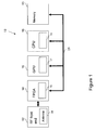
- the SDR device 10 includes a RF front end 12 having an antenna 28 for receiving and converting electromagnetic radiation into a digital signal, a field programmable gate array (FPGA) 14 for performing high speed serial processing and a graphics processing unit (GPU) 16 for performing parallel processing.
- the SDR device 10 may also include a general purpose computer processing unit (CPU) 18 for performing general computations including providing the user interface and programming the FPGA 14 and GPU 16.
- the FPGA 14, GPU 16 and CPU 18 can each have its own memory 15, 17 and 19, respectively and/or can access a separate memory component 13 of the device 10. It is understood that the FPGA 14 can include any suitable programmable logic device and GPU 16 includes general purpose computing on graphics processing unit ((GP)GPU).
- GP general purpose computing on graphics processing unit
- the RF front end 12 is connected to the FPGA 14 and is operable to communicate with the FPGA 14 by a plurality of digital signals.
- the FPGA 14, GPU 16 and CPU 18 are connected to one another by a high speed bus 21, such as a Peripheral Component Interconnect Express (PCIe) bus, for example.
- PCIe Peripheral Component Interconnect Express
- the SDR device 10 enables rapid serial and parallel computation of signal processing data.
- the SDR device 10 can divide signal processing algorithms into block and streaming processes and implement the block and stream processes to optimize processing efficiency.
- Stream processing may segment the input signal into a plurality of discrete segments or "chunks" based, in part, on the current state of the input signal passing through it, while block processing may comprise fixed, invariant, processing on each chunk.
- the FPGA 14 provides a fast serial processing environment to perform stream processing.
- the GPU 16 provides a parallel processing 22276050.1 environment to parallelize block processes.
- the GPU 16 thus effectively implements parallelizable calculations and algorithms, including, for example, weak signal reconstruction, auto-correlation, FFTs, mutual information metrics, as well as concurrent processing of arbitrary algorithms or calculations on single or multiple data streams.
- the programmability of the FPGA 14 and the GPU 16 also provides flexibility, such that the SDR device 10 may be capable of running arbitrary wireless protocols.
- FPGA 14 and GPU 16 can be reprogrammed by CPU 18 during operation to handle changes in the communication protocol on an input signal. Once programmed, the SDR device 10 can autonomously store and send data without requiring additional configuration or intervention.
- the SDR device 10 can also be configured to concurrently monitor spectral and network resources and adjust transmission and receiving parameters accordingly. Furthermore, the SDR device 10 can manage its own resources (e.g.. FPGA 14 and GPU 16) such that tasks are efficiently allocated to the appropriate component based on the type of computation and resource usage.
- resources e.g.. FPGA 14 and GPU 16
- the SDR device 10 is operable to identify and intercept a radio signal comprising one or more radio frequency bands, extract one or more channels from the radio signal, the radio signal having a bandwidth at least as wide as each channel, and process one or more channels in parallel.
- the SDR device 10 is applied to a radio signal comprising a plurality of radio frequency bands.
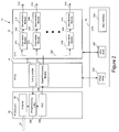
- the SDR device 10 has an RF front end 12 which includes an antenna 28 to receive a radio signal 22, a pre-processing utility 302 to isolate a band of frequencies in the radio signal 22 and to process the radio signal 22 for digitization, and an analog to digital converter (ADC) 304 to convert the pre-processed radio signal 22 into a digital signal 306.
- a tuning module 310 of the FPGA 14 may determine and provide a centre frequency and filter parameters to configure the pre-processing utility 302 to isolate a band of frequencies centred around the centre frequency and having a width based on the filtering parameters.
- the digital signal 306 produced by the ADC 304 is sent to the FPGA 14.
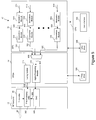
- the RF front end pre-processes the radio signal 22 by amplification and down-conversion prior to digitization.
- the RF front end includes an antenna 28 to intercept the radio signal 22 and may include pre-processing components such as a low noise amplifier (LNA) 402 to amplify weak signals, a high pass filter (HPF) 404 to filter and pass high frequencies and attenuate low frequencies, an amplifier (e.g.
- LNA low noise amplifier
- HPF high pass filter
- variable gain block 406 and/or variable gain amplifier 408 a variable attenuator 410 to vary the signal gain
- a down-converter 412 to down-convert the signal to baseband
- ADC analog to digital converter
- driver 416 and anti-aliasing filter 418 to improve the quality of the ADC conversion.
- the RF front end 12 has two modes of operation A and B, selectable by a switch 420. Each mode of operation performs a series of operations on the radio signal 22 before digitization by the ADC 304.
- the first mode of operation A is selected.
- the radio signal 22 intercepted by the antenna 28 is amplified by the LNA 402 and filtered using the HPF 404.
- the gain of the radio signal 22 is then modified using gain block 406 and variable attenuator 410.
- the resulting signal is then down-converted by first mixing in a signal generated by the local oscillator 422 using mixer 412.
- the local oscillator 422 is configured to generate a signal at the centre frequency provided by the tuning module 310 of the FPGA 14.
- the mixed signal can be phase shifted by phase converter 424, further amplified by driver 416 and filtered by anti-aliasing filter 418 to produce a baseband signal prior to digitization using the ADC 304.
- the resulting digital signal 306 is decomposed into its quadrature-carrier (IQ) form made of the in-phase component 306a, and the quadrature component 306b.
- the cut off frequency of the baseband signal can be determined by the anti-aliasing filters 418 and can be configured based on the application of the SDR device 10.
- the SDR device 10 can tune into and isolate a specific band of frequencies in the radio signal 22.
- the RF front end 12 can be any appropriate receiver capable of isolating the frequency band of interest and digitizing the radio signal 22.
- the analog signal received by the antenna 28 can be amplified by LNA 402 and filtered using HPF 404, as in first mode of operation A. However, the analog signal can then be amplified using variable gain amplifier 408 and directly applied to ADC 304.
- the SDR device 10 in this example also has an FPGA 14 configured to include a tuning module 310 for providing the pre-processing stage 302 of the RF front end 12 with a centre frequency and filtering parameters and a digital processing module 312 for digitally processing the digital signal 306.
- the digital processing module 312 implements a digital up/down converter on the FPGA 14 to isolate a band of frequencies within the digital signal 306. Further up or down conversion carried out by the digital processing module 312 can correct or reduce an error in the analog down conversion carried out by the RF front end 12.
- the digital processing module 312 carries out filtering and/or decimation on the digital signal 306 to reduce the bandwidth of the digital signal 306 (for example, to satisfy the bandwidth limit of the high speed bus 21 connecting the FPGA 14 to the GPU 16). This allows the FPGA 14 to negotiate data transfers over the bus 21.
- the digital processing module 312 can implement a digital low pass filter to reduce the width of the frequency band of the digital signal 306 and/or implement a digital downsampler to decimate the digital signal 306.
- the digital processing module 312 can operate as the primary module for extracting the desired band of frequencies from the radio signal 22.
- the digital processing module 312 can implement multiple instances of digital up/down converters and filters to isolate more than one band of frequencies from the digital signal 306.
- the FPGA 14 can route the digital signal 306 to one or more of its modules, its internal memory, and/or bypass the FPGA processing all together, by configuring the programmable switches provided by the FPGA. For example, certain data may not require further down-conversion of the digital signal 306.
- the selection and passage of the any signal within FPGA 14 can be set according to the desired application using appropriately configured switches.
- the SDR device 10 in the example also has a GPU 16 configured to include a plurality of channelizer modules 316 for extracting a channel 320 from the processed digital signal 322 and a plurality of demodulation modules 318 to carry out demodulation of a channel 320 to produce a demodulated signal 314.
- Each channelizer module 316 can separate a specific frequency sub-band (i.e. channel 320) from the processed digital signal 322 containing a band of frequencies.
- the channelizer module 316 is a digital up/down converter implemented on the GPU 16.
- the channelizer module 316 down converts or up converts the desired sub band to baseband depending on whether the desired band contains positive or negative frequencies.
- the down or up conversion of frequency can be followed by filtering using a low pass filter to determine the frequency width of the channel and subsequently decimated using a downsampler.
- a channelizer module 316 can operate in parallel with one or more other channelizer modules 316 to extract multiple channels 320 from the processed digital signal 322 and provide the channels 320 to a plurality of demodulation modules 318 for further processing.
- each channelizer module 316 provides the extracted channel 320 to a respective demodulation module 318.
- the demodulation modules 318 can operate on its respective channel 320 in parallel with the operation of other demodulation modules 318 to produce its respective demodulated signal 314.
- the demodulated signals 314 can be further processed based on the desired application. For example, a demodulated signal 314 can be combined with one or more other demodulated signals 314, stored in memory, further processed by the CPU, or independently viewed by the user on a computer.
- the GPU 16 can have one or more demodulation modules 318 to carry out one or more different demodulation techniques on the FPGA output 322, such as demodulation of a radio signal modulated using amplitude modulation (AM), frequency modulation (FM) and single-sideband modulation (SSB).
- Each demodulation module 318 can also apply demodulation to one or more different communication protocols (for example Global System for Mobile Communications (GSM) or Zigbee).
- GSM Global System for Mobile Communications
- the modulation techniques and communication protocols can be configured by the user or provided by third parties.
- the demodulation modules 318 can be reprogrammed during operation to implement a different modulation technique and/or communication protocol. Accordingly, the demodulation module 318 allows for different modulation techniques and communication protocols to be determined and implemented dynamically (on the fly) while the device remains operational.
- RF front end 12 intercepts an radio signal 22 using its antenna 28.
- the device 10 obtains tuning parameters related to a band of frequencies that are to be extracted from the radio signal 22, such as the centre frequency and filter parameters.
- RF front end 12 extracts a band of frequencies from the radio signal 22 to generate a baseband signal.
- RF front end 12 digitizes the baseband signal using its ADC 304 to generate a digital signal 306.
- FPGA 14 digitally processes the digital signal 306, for example, by further down or up converting the digital signal to compensate for errors introduced in the extraction of a band of frequencies from the radio signal 22.
- GPU 16 extracts one or more band of frequencies from the digital signal 306 to generate one or more channels using the channelizer modules 316.
- GPU 16 demodulates each channel 320 using its demodulation module 318 to generate a demodulated signal 314.
- FPGA 14 can digitally process the digital signal 306 containing a band of frequencies using the digital processing module 312.
- the FPGA 14 can improve or correct errors introduced during extraction of the desired band of frequencies by the RF front end 12 by configuring the digital processing module to implement a suitable digital up or down converter to translate the frequency band of the digital signal 306.
- the digital processing module can be configured to implement a suitable digital low pass filter and downsampler to filter and decimate the digital signal 306 in order to reduce its bandwidth.
- GPU 16 extracts one or more band of frequencies from the digital signal 306 to generate one or more channels.
- each channel is demodulated to generate a corresponding demodulated signal 314.
- the GPU 16 includes multiple channelizer modules 316, each having a respective demodulation module 318.
- the channelizer modules 316 and demodulation modules 318 can operate in parallel so that multiple channels are extracted and demodulated simultaneously, thus taking advantage of the parallel processing capabilities of the GPU 16.
- each channelizer module 316 extracts a different band of frequencies from the digital signal 306 to be demodulated by the same or different demodulation schemes in the demodulation modules 318.
- more than one channelizer module 316 can extract the same band of frequencies but have different demodulation performed by its respective demodulation module 318.
- the radio signal 22 received by the SDR device 10 can include multiple signals broadcast on the same or similar frequencies but having different timing characteristics. The SDR device 10 can provide concurrent processing of the same frequency on different channels to accommodate multiple but similar broadcasting sources.
- the process of extracting and demodulating one or more channels in a radio signal can also include averaging the demodulated signal 314, as shown at block 514.
- the demodulating module 318 of the example SDR device 10 can perform time domain averaging on a segment of the demodulated signal 314 with one or more previous segments of the same demodulated signal 314 to improve the quality of the demodulated signal 314.
- the demodulating module 318 can average a demodulated signal 314 of one channel 320 with one or more demodulated signals 314 of another channel 320. For example, if the band of frequencies in the digital signal 306 corresponds to the frequency components of a common signal, the channels extracted by the SDR device would correspond to the frequency components of the common signal.
- the demodulating module 318 can also average a plurality demodulated signals 314 of different channels 320 to provide frequency domain averaging of multiple samples (at a given point in time) to improve signal quality and reduce measurement errors.
- different demodulated signals 314 can be compared, cross-correlated, or otherwise analyzed for similarities, statistical metrics, etc. to improve the quality of a demodulated signal 314.
- An example application of the SDR device 10 is a FM radio receiver capable of concurrently tuning into, and recording multiple channels (corresponding to an FM radio station) in the FM radio band.
- FM radio currently broadcasts using frequencies between 88.0 and 108.0 MHz, each channel being 200 kHz wide and centered about 0.1, 0.3, 0.5, 0.7, or 0.9 MHz.
- the SDR device 10 can be configured to have a centre frequency of 88 MHz and filtering parameters such that the cut off frequency of the baseband signal is 20 MHz.
- the RF front end 12 can extract and down convert the band of frequencies from 88.0 to 108.0 MHz in the radio signal 22 to a baseband signal from 0 Hz to 20 MHz using the pre-processing utility 302 of the RF front end 12. This allows the baseband signal to contain the information of the entire FM radio band.
- the RF front end 12 can then digitize the baseband signal using its ADC 304 to generate a digital signal 306 which is then passed to the FPGA 14 for digital processing such as filtering, decimation, IQ demodulation, etc.
- each channelizer module 316 of the GPU 16 can shift and decimate the digital signal 306 to extract a band of frequencies of width 200 kHz centered about 0.1, 0.3, 0.5, 0.7, or 0.9 MHz, corresponding to the information broadcasted by a FM radio station.
- the demodulation modules 318 can be configured to perform FM demodulation to recover the information in the FM radio broadcast such as audio data, pilot tones, etc.
- the SDR device 10 has been described for extracting and demodulating a plurality of channels from a radio signal, it can be appreciated that the SDR device 10 can be modified to be operable to modulate one or more signals across one or more frequencies and to combine the modulated signals into a common signal for transmission.
- complementary components and modules can be used to replace those described in FIGS. 2 and 3 of the example SDR device 10.
- complementary operations can be used to replace those described in the example process of FIG. 4 .
- FIG. 5 a block diagram of an example configuration of the SDR device 10' for the specific application of modulating and combining a plurality of channels is provided.
- the SDR device 10' in the example has a GPU 16 configured to include a plurality of modulation modules 618 to carry out modulation of an input signal 614 to produce a respective modulated signal 620 and a plurality of channelizer modules 316 for translating a modulated signal 620 to a specific band of frequencies to generate a channel 320.
- each modulation module 618 can operate on its respective input signal 614 in parallel with the operation of other modulation modules 618 to produce its respective modulated signal 620.
- each modulation module 618 provides its modulated signal 620 to a respective channelizer module 316.
- the GPU 16 can have one or more modulation modules 618 to carry out one or more different modulation techniques, such as amplitude modulation (AM), frequency modulation (FM) and single-sideband modulation (SSB).
- Each modulation module 618 can also apply modulation to one or more different communication protocols (for example GSM or Zigbee).
- the modulation techniques and communication protocols can be configured by the user or provided by third parties.
- the modulation modules 618 can be reprogrammed during operation to implement a different modulation technique and/or communication protocol. Accordingly, the modulation module 618 allows for different modulation techniques and communication protocols to be determined and implemented dynamically (on the fly) while the device remains operational.
- Each channelizer module 316 can translate a modulated signal 620 to specific frequency sub band (i.e. channel 320) of a band of frequencies that will make up the combined signal 622.
- the channelizer module 316 is a digital up/down converter implemented on the GPU 16.
- the channelizer module 316 down converts or up converts the modulated signal 620 depending on the desired sub band (i.e. channel 320) desired to contain the modulated signal 620. It can be appreciated that one or more modulation modules 618 and channelizer modules 316 can operate in parallel on the GPU 16.
- the SDR device 10' in this example also has an FPGA 14 configured to include a multiplexer 630 to combine one or more channels 320 provided by the GPU 16 to generate a combined signal 622, a digital processing module 312 for digitally processing the combined signal 622 in preparation of digital to analog conversion, and a tuning module 310 for providing transmission parameters (such as centre frequency and filtering parameters) to the RF front end 12.
- FPGA 14 configured to include a multiplexer 630 to combine one or more channels 320 provided by the GPU 16 to generate a combined signal 622, a digital processing module 312 for digitally processing the combined signal 622 in preparation of digital to analog conversion, and a tuning module 310 for providing transmission parameters (such as centre frequency and filtering parameters) to the RF front end 12.
- a multiplexer 630 implemented on the FPGA 14 is used in the example SDR device 10' to combine one or more channels 320. It can be appreciated that the multiplexer 630 can be implemented on the GPU 16 or that a combination of multiplexers 630 may be used implemented on both the FPGA 14 and GPU 16.
- multiple digital processing modules 312 may be implemented on the FPGA 14, each digital processing module 312 receiving a subset of all channels 320.
- the digitally processed signals of each digital processing module 312 can then be combined by one or more multiplexers in the RF front end 12. This allows the SDR device 10' to group similar frequency channels together for processing and optimizing processing for that particular band of frequencies.
- the digital processing module 312 implements a digital up and/or down converter.
- the digital processing module 312 can also be configured to perform filtering on the combined signal 622 prior to digital to analog conversion. Examples of such filters include linear filters to reduce spurious emissions and nonlinear filters which can compensate for nonlinearities in the RF front end 12.
- the example SDR device 10' also has an RF front end 12 which includes a digital to analog converter (DAC) 604 to convert the digitally processed combined signal 622 into an analog signal 606, a pre-processing utility 302 to translate the frequency band of the analog signal 606 to the desired band of frequencies for transmission, and a transmitter (e.g. antenna) for transmitting the analog output signal 62.
- a tuning module 310 of the FPGA 14 may determine and provide a centre frequency and filter parameters to configure the pre-processing utility 302 to translate the analog signal 606 to a band of frequencies centred around the centre frequency and having a width of frequencies based on the filtering parameters.
- the analog signal 606 is processed by the pre-processing utility 302 using the centre frequency and filtering parameters and then sent to the transmitter 68 for transmission.
- one or more input signals 614 are obtained by the GPU 16.
- the input signals 614 can be provided by the FPGA 14 or CPU 18.
- an input signal 614 can be provided from the demodulated signal 314 of the example SDR device 10.
- input signals 614 are modulated to generate a respective modulated signal 620.
- the modulation modules 318 of the GPU 16 modulate the input signals 614.
- a plurality of modulation modules 318 operate in parallel to modulate multiple input signals 614 concurrently.
- each modulated signal 620 is translated to a band of frequencies to generate a respective channel 320.
- the channelizer modules 318 translate the modulated signals 620 to a band of frequencies.
- each modulated signal 620 is translated to a different band of frequencies.
- more than one modulated signal 620 can be translated to the same frequency.
- a plurality of channelizer modules 316 can operate in parallel.
- each channel 320 is combined to generate a combined signal 622.
- a multiplexer 630 implemented on the FPGA 14 combines each channel 316 into the combined signal 622.
- the combined signal 622 is digitally processed.
- the combined signal 622 is prepared for improved digital to analog conversion.
- the digital processing module 312 of the FPGA 14 digitally processes the combined signal 622.
- the digital combined signal 622 is converted to an analog signal 606.
- the DAC 604 of the RF front end 12 performs the conversion.
- the analog signal 606 is translated to the desired band of frequencies.
- the pre-processing utility 302 of the RF front end 12 performs the translation, using a centre frequency and filtering parameters provided by the tuning module 310 of the FPGA. 14.
- the analog signal 606 is transmitted.
- the transmitter 68 e.g. an antenna
- the RF front end transmits the analog signal 606.
- An example application of the SDR device 10' of FIG. 5 is to transmit audio data on multiple FM radio channels concurrently.
- audio data of each genre can serve as an input signal 614 to a modulation module 618 for frequency modulating the audio data of each genre on to a different channel.
- the multiplexer 630 combines each channel into the combined signal 622 which is then be translated to a frequency band within the FM radio frequency band (i.e. 88.0 and 108.0 MHz) by the pre-processing utility 302 of the RF front end 12.
- the output signal 62 transmitted by the SDR device 10' contains audio data of each genre on separate FM radio channels that can be received by other FM radio devices.
- the SDR device 11 can combine the frequency components into the combined signal 622 to more accurately replicate the original signal because the combined signal 622 contains more frequency components than an individual input signal 614.
- the input signal 614 of the example SDR device 10' can correspond to the demodulated signal 314 of the example SDR device 10.
- the SDR devices 10 and 10' can be implemented on a common RF front end 12, FPGA 14, GPU 16 and CPU 18 to create one SDR device capable of performing the functionality of both SDR devices 10 and 10'.
- modules implemented on a component of SDR devices 10 and 10' may be combined.
- a SDR device can intercept a radio signal 22 having multiple channels 320 of information and demodulate each channel 320 according to a particular communication and demodulation protocol using the example process of FIG. 5 .
- the same SDR device can then modulate and transmit each demodulated signal 314 according to a different communication and/or modulation protocol that does not correspond to the communication and/or modulation protocol of the channels in the radio signal 22 using the example process of FIG. 7 .
- Example communication and modulation protocols that can be used include AM, SSB, Quadrature Amplitude modulation (QAM), GSM, Code Division Multiple Acces (CDMA), Global Packet Radio Service (GPRS), etc.
- the SDR device can translate information between different frequencies, modulation/demodulation protocols and/or communication protocols to allow communication between devices using different frequencies, modulation/demodulation protocols and/or communication protocols.
- the SDR device can receive the radio signal 22 containing information transmitted by a mobile device under a cellular communication protocol such as GSM or CDMA and rebroadcast the information over a different wireless network such as Wifi.
- the radio signal can be translated and transmitted through a wired connection to a local area network (LAN).
- LAN local area network
- the SDR devices 10 and 10' can also include a CPU 18 configured to provide a user interface 324 for allowing a user to interact with the SDR device 10.
- the CPU 18 includes a GPU driver 326 and a FPGA driver 328.
- the drivers 326 and 328 enable the CPU 18 to communicate with the FPGA 14 and GPU 16 (for example, to program the FPGA 14 and GPU 16).
- the application layer 900 includes a SDR API 902 that provides the rules and specifications to access the components of the device 10, such as GPU 16 and FPGA 14.
- Each component also has its own driver to interface with the SDR API 902 (e.g. GPU driver 326, FPGA driver 328).
- a user can access the device 10 using the user interface 324, which can include a command line interface (CLI) 904, web user interface (Web UI) 906 and/or graphical user interface (GUI) 908, enabling communication with the device resources through the API 902.
- the API 902 can provide access to a local or remote memory 910 (e.g. remote memory can be accessible through a network).
- the local or remote memory 910 can store GPU programs and FPGA bit streams 912 used to operate the SDR device 10.
- the application layer 900 provides a common API to remote users connecting to the SDR device 10.
- the user can connect to the device for the purpose of receiving data from the SDR device 10, injecting data to be transmitted by SDR device 10, or for configuring the SDR device 10. It can be appreciated that the device 10 may be programmed to allow it to autonomously act to capture, transmit, store, or communicate with other devices.
- the application layer 900 also provides a means by which processed data may be sent over another, possibly lower bandwidth, connection to remote users.
- the application layer 900 can provide a mechanism by which remote users may access and retrieve stored data, as well as modify and program the behaviour of the device 10.
- the Web UI 906 is operable to allow communication between the SDR device 10 and a remote user over the internet.
- connections to the SDR device 10 can be made through an internet communication protocol such as Transmission Control Protocol / Internet Protocol (TCP/IP).
- TCP/IP Transmission Control Protocol / Internet Protocol
- a user can remotely communicate with the SDR device 10 using a third party web browser or SDR specific computer software.
- GPU programs and FPGA bit streams 912 can be transferred over the network using a networking protocol such as Hypertext Transfer Protocol (HTTP) POST commands.
- HTTP Hypertext Transfer Protocol
- the Web UI 906 can receive GPU programs and send them to the GPU 16 via the SDR API 902 and GPU driver 326.
- the Web UI 906 can receive FPGA bitstreams and send them to the FPGA 14 via the SDR API 902 and the FPGA driver 328.
- the Web UI 906 can also be operable to allow a user to configure and control the behaviour of the SDR device 10 through HTTP GET commands, for example.
- the Web UI 906 can translate the HTTP GET commands to API calls for the SDR API 902.
- software running on the SDR device 10 is not constrained to one physical component. It may run on the CPU 18, GPU 16, FPGA 14 and/or RF front end 12. Each physical component can perform a different computational task.
- CPU 18 or FPGA 14 can provide a user interface, retrieve and store data from memory, and dynamically program and configure GPU 16 and RF front end 12.
- the GPU 16 can run computationally intensive tasks such as spectrum analysis and cryptanalysis.
- the RF front end 12 can provide the analog means necessary for a desired application.
- the SDR 10 can perform management activities. This can include using the signal or spectral information to manage the connection or communication itself. Management activity can also include monitoring the network or ambient RF environment to modify the communication protocols parameters to optimize transmission, reception and other communication characteristics.
- the SDR device 10 may be operable to redefine its transmission parameters independently, based on predefined algorithms or in concert with other devices. These cognitive algorithms may be calculated on the FPGA 14 or parallelized and calculated on the GPU 16.
Description
- The present invention relates to radio communication systems, and in particular to software defined radio systems.
- Traditionally, development of radio communication products involves significant hardware development effort. Software defined radio (SDR) is a technology that implements physical layer wireless communication technologies in software, turning many radio-related hardware development problems into software issues. This can shorten the product development cycle, reduce costs, and make product distribution much easier. Moreover, SDR provides increased flexibility and programmability, which can speed up innovation in wireless communications.
- SDR platforms have been developed using a personal computer's central processing unit (CPU), working in connection with a field programmable gate array (FPGA), with some radio frequency (RF) front end hardware to receive and transmit radio waveforms. Some SDR applications require complex modulation or computationally intensive algorithms that may include Fast Fourier Transforms (FFTs), cross-correlation, or the calculation of mutual information metrics. These operations can be costly in terms of processing power. A CPU working in connection with an FPGA may lack the computing architecture to support these applications. More recently, SDR platforms have been developed using a CPU working in connection with a graphics processing unit (GPU). However, a GPU working in connection with a CPU may lack the streaming or serial processing capabilities to fulfill the real-time requirements of digital communication algorithms that perform serial processing.
- It is an object of the present invention to obviate or mitigate one or more of the above disadvantages.
- An example of a software defined radio is disclosed in
US 5289464 . - In one aspect, there is provided a method of extracting and demodulating one or more channels in a radio signal according to claim 1.
- In another aspect, there is provided a method of modulating and combining one or more channels into a radio signal in accordance with
claim 10 - In another aspect, an electronic device, such as an SDR device, is provided. The electronic device includes a RF front end, a processing unit and memory. The memory stores computer executable instructions that when executed by the processing unit, causes the electronic device to perform a method according to claim 1.
- In another aspect, another electronic device, such as an SDR device, is provided. The electronic device includes a RF front end, a processing unit and memory. The memory stores computer executable instructions that when executed by the processing unit, causes the electronic device to perform a method according to
claim 10. - In another aspect, a computer readable storage medium is provided for extracting and demodulating one or more channels in a radio signal. The computer readable storage medium includes computer executable instructions that when executed by a processing unit, causes the processing unit perform a method according to claim 1.
- In another aspect, a computer readable storage medium is provided for modulating and combining one or more channels into a radio signal. The computer readable storage medium includes computer executable instructions that when executed by a processing unit, causes the processing unit to perform a method according to
claim 10. - In another aspect which is not independently claimed, there is provided a SDR device comprising a RF front end, a FPGA in communication with the RF front end and a GPU in communication with the FPGA. The RF front end is operable to receive and transmit one or more radio signals. The FPGA is operable to perform serial processing on one or more digital signals corresponding to the one or more radio signals. The GPU is operable to perform parallel processing on the one or more digital signals. The SDR device can also include a CPU in communication with at least one of the FPGA and GPU for performing general computations such as providing a user interface and programming the FPGA and/or GPU.
- Embodiments of the invention will be described by way of example only with reference to the accompanying drawings in which:
-
FIG. 1 is a block diagram of an example SDR device; -
FIG. 2 is a block diagram of an example configuration of a SDR device for the specific application of extracting and demodulating channels in a radio signal; -
FIG. 3 is a schematic diagram of an example RF front end; -
FIG. 4 is a flow chart of an example process of extracting and demodulating channels in a radio signal using an example SDR device; -
FIG. 5 is a block diagram of an example configuration of a SDR device for the specific application of modulating and combining a plurality of channels; -
FIG. 6 is a flow chart of an example process of modulating and combining a plurality of channels using an example SDR device; and -
FIG. 7 is a block diagram of an example application layer of the SDR device. - It will be appreciated that for simplicity and clarity of illustration, where considered appropriate, reference numerals may be repeated among the figures to indicate order to provide a thorough understanding of the example embodiments described herein. However, it will be understood by those of ordinary skill in the art that the example embodiments described herein may be practised without these specific details.
- In other instances, well-known methods, procedures and components have not been described in detail so as not to obscure the example embodiments described herein. Also, the description is not to be considered as limiting the scope of the example embodiments described herein.
- Turning to
FIG. 1 , a schematic diagram of anexample SDR device 10 is provided. In this example, theSDR device 10 includes aRF front end 12 having anantenna 28 for receiving and converting electromagnetic radiation into a digital signal, a field programmable gate array (FPGA) 14 for performing high speed serial processing and a graphics processing unit (GPU) 16 for performing parallel processing. TheSDR device 10 may also include a general purpose computer processing unit (CPU) 18 for performing general computations including providing the user interface and programming theFPGA 14 andGPU 16. TheFPGA 14,GPU 16 andCPU 18 can each have itsown memory separate memory component 13 of thedevice 10. It is understood that theFPGA 14 can include any suitable programmable logic device andGPU 16 includes general purpose computing on graphics processing unit ((GP)GPU). - In the example of
FIG. 1 , theRF front end 12 is connected to theFPGA 14 and is operable to communicate with theFPGA 14 by a plurality of digital signals. The FPGA 14, GPU 16 andCPU 18 are connected to one another by ahigh speed bus 21, such as a Peripheral Component Interconnect Express (PCIe) bus, for example. - The
SDR device 10 enables rapid serial and parallel computation of signal processing data. For example, theSDR device 10 can divide signal processing algorithms into block and streaming processes and implement the block and stream processes to optimize processing efficiency. Stream processing may segment the input signal into a plurality of discrete segments or "chunks" based, in part, on the current state of the input signal passing through it, while block processing may comprise fixed, invariant, processing on each chunk. - In one
example SDR device 10, theFPGA 14 provides a fast serial processing environment to perform stream processing. The GPU 16 provides a parallel processing 22276050.1 environment to parallelize block processes. TheGPU 16, thus effectively implements parallelizable calculations and algorithms, including, for example, weak signal reconstruction, auto-correlation, FFTs, mutual information metrics, as well as concurrent processing of arbitrary algorithms or calculations on single or multiple data streams. - The programmability of the
FPGA 14 and theGPU 16 also provides flexibility, such that theSDR device 10 may be capable of running arbitrary wireless protocols. For example, FPGA 14 andGPU 16 can be reprogrammed byCPU 18 during operation to handle changes in the communication protocol on an input signal. Once programmed, theSDR device 10 can autonomously store and send data without requiring additional configuration or intervention. - The
SDR device 10 can also be configured to concurrently monitor spectral and network resources and adjust transmission and receiving parameters accordingly. Furthermore, theSDR device 10 can manage its own resources (e.g.. FPGA 14 and GPU 16) such that tasks are efficiently allocated to the appropriate component based on the type of computation and resource usage. - In an example application of the
SDR device 10, it is operable to identify and intercept a radio signal comprising one or more radio frequency bands, extract one or more channels from the radio signal, the radio signal having a bandwidth at least as wide as each channel, and process one or more channels in parallel. Preferably, theSDR device 10 is applied to a radio signal comprising a plurality of radio frequency bands. - Referring to
FIG 2 , a block diagram of an example configuration of theSDR device 10 for the specific application of extracting and demodulating a plurality of channels in a radio signal is provided. TheSDR device 10 has an RFfront end 12 which includes anantenna 28 to receive aradio signal 22, apre-processing utility 302 to isolate a band of frequencies in theradio signal 22 and to process theradio signal 22 for digitization, and an analog to digital converter (ADC) 304 to convert thepre-processed radio signal 22 into adigital signal 306. Atuning module 310 of theFPGA 14 may determine and provide a centre frequency and filter parameters to configure thepre-processing utility 302 to isolate a band of frequencies centred around the centre frequency and having a width based on the filtering parameters. Thedigital signal 306 produced by theADC 304 is sent to theFPGA 14. - Turning to
FIG. 3 , a more detailed schematic diagram of an example RFfront end 12 is provided. The RF front end pre-processes theradio signal 22 by amplification and down-conversion prior to digitization. The RF front end includes anantenna 28 to intercept theradio signal 22 and may include pre-processing components such as a low noise amplifier (LNA) 402 to amplify weak signals, a high pass filter (HPF) 404 to filter and pass high frequencies and attenuate low frequencies, an amplifier (e.g. gain block 406 and/or variable gain amplifier 408), avariable attenuator 410 to vary the signal gain, a down-converter 412 to down-convert the signal to baseband, an analog to digital converter (ADC) 304, and adriver 416 andanti-aliasing filter 418 to improve the quality of the ADC conversion. - In the example of
FIG. 3 , the RFfront end 12 has two modes of operation A and B, selectable by aswitch 420. Each mode of operation performs a series of operations on theradio signal 22 before digitization by theADC 304. InFIG. 3 , the first mode of operation A is selected. Theradio signal 22 intercepted by theantenna 28 is amplified by theLNA 402 and filtered using theHPF 404. The gain of theradio signal 22 is then modified usinggain block 406 andvariable attenuator 410. The resulting signal is then down-converted by first mixing in a signal generated by thelocal oscillator 422 usingmixer 412. Thelocal oscillator 422 is configured to generate a signal at the centre frequency provided by thetuning module 310 of theFPGA 14. The mixed signal can be phase shifted byphase converter 424, further amplified bydriver 416 and filtered byanti-aliasing filter 418 to produce a baseband signal prior to digitization using theADC 304. In this example, the resultingdigital signal 306 is decomposed into its quadrature-carrier (IQ) form made of the in-phase component 306a, and thequadrature component 306b. The cut off frequency of the baseband signal can be determined by theanti-aliasing filters 418 and can be configured based on the application of theSDR device 10. - By modifying the centre frequency and filter parameters, the
SDR device 10 can tune into and isolate a specific band of frequencies in theradio signal 22. It can be appreciated that the RFfront end 12 can be any appropriate receiver capable of isolating the frequency band of interest and digitizing theradio signal 22. - In the second mode of operation B of the example RF
front end 12 ofFIG. 3 , the analog signal received by theantenna 28 can be amplified byLNA 402 and filtered usingHPF 404, as in first mode of operation A. However, the analog signal can then be amplified usingvariable gain amplifier 408 and directly applied toADC 304. - Turning back to
FIG. 2 , theSDR device 10 in this example also has anFPGA 14 configured to include atuning module 310 for providing thepre-processing stage 302 of the RFfront end 12 with a centre frequency and filtering parameters and adigital processing module 312 for digitally processing thedigital signal 306. In one embodiment, thedigital processing module 312 implements a digital up/down converter on theFPGA 14 to isolate a band of frequencies within thedigital signal 306. Further up or down conversion carried out by thedigital processing module 312 can correct or reduce an error in the analog down conversion carried out by the RFfront end 12. In another embodiment, thedigital processing module 312 carries out filtering and/or decimation on thedigital signal 306 to reduce the bandwidth of the digital signal 306 (for example, to satisfy the bandwidth limit of thehigh speed bus 21 connecting theFPGA 14 to the GPU 16). This allows theFPGA 14 to negotiate data transfers over thebus 21. Thedigital processing module 312 can implement a digital low pass filter to reduce the width of the frequency band of thedigital signal 306 and/or implement a digital downsampler to decimate thedigital signal 306. - In the example of an RF
front end 12 operating in mode B, thedigital processing module 312 can operate as the primary module for extracting the desired band of frequencies from theradio signal 22. In one embodiment, thedigital processing module 312 can implement multiple instances of digital up/down converters and filters to isolate more than one band of frequencies from thedigital signal 306. - It can further be appreciated that the
FPGA 14 can route thedigital signal 306 to one or more of its modules, its internal memory, and/or bypass the FPGA processing all together, by configuring the programmable switches provided by the FPGA. For example, certain data may not require further down-conversion of thedigital signal 306. The selection and passage of the any signal withinFPGA 14 can be set according to the desired application using appropriately configured switches. - The
SDR device 10 in the example also has aGPU 16 configured to include a plurality ofchannelizer modules 316 for extracting achannel 320 from the processeddigital signal 322 and a plurality ofdemodulation modules 318 to carry out demodulation of achannel 320 to produce ademodulated signal 314. - Each
channelizer module 316 can separate a specific frequency sub-band (i.e. channel 320) from the processeddigital signal 322 containing a band of frequencies. In one example embodiment, thechannelizer module 316 is a digital up/down converter implemented on theGPU 16. Thechannelizer module 316 down converts or up converts the desired sub band to baseband depending on whether the desired band contains positive or negative frequencies. The down or up conversion of frequency can be followed by filtering using a low pass filter to determine the frequency width of the channel and subsequently decimated using a downsampler. - A
channelizer module 316 can operate in parallel with one or moreother channelizer modules 316 to extractmultiple channels 320 from the processeddigital signal 322 and provide thechannels 320 to a plurality ofdemodulation modules 318 for further processing. In the example ofFIG. 2 , eachchannelizer module 316 provides the extractedchannel 320 to arespective demodulation module 318. Thedemodulation modules 318 can operate on itsrespective channel 320 in parallel with the operation ofother demodulation modules 318 to produce itsrespective demodulated signal 314. The demodulated signals 314 can be further processed based on the desired application. For example, ademodulated signal 314 can be combined with one or more otherdemodulated signals 314, stored in memory, further processed by the CPU, or independently viewed by the user on a computer. - It can be appreciated that the
GPU 16 can have one ormore demodulation modules 318 to carry out one or more different demodulation techniques on theFPGA output 322, such as demodulation of a radio signal modulated using amplitude modulation (AM), frequency modulation (FM) and single-sideband modulation (SSB). Eachdemodulation module 318 can also apply demodulation to one or more different communication protocols (for example Global System for Mobile Communications (GSM) or Zigbee). The modulation techniques and communication protocols can be configured by the user or provided by third parties. Furthermore, thedemodulation modules 318 can be reprogrammed during operation to implement a different modulation technique and/or communication protocol. Accordingly, thedemodulation module 318 allows for different modulation techniques and communication protocols to be determined and implemented dynamically (on the fly) while the device remains operational. - Turning to
FIG. 4 , a flow chart of an example process for extracting and demodulating one or more channels in aradio signal 22 is provided. Atblock 500, RFfront end 12 intercepts anradio signal 22 using itsantenna 28. Atblock 502, thedevice 10 obtains tuning parameters related to a band of frequencies that are to be extracted from theradio signal 22, such as the centre frequency and filter parameters. Atblock 504, RFfront end 12 extracts a band of frequencies from theradio signal 22 to generate a baseband signal. Atblock 506, RFfront end 12 digitizes the baseband signal using itsADC 304 to generate adigital signal 306. Atblock 508,FPGA 14 digitally processes thedigital signal 306, for example, by further down or up converting the digital signal to compensate for errors introduced in the extraction of a band of frequencies from theradio signal 22. Atblock 510,GPU 16 extracts one or more band of frequencies from thedigital signal 306 to generate one or more channels using thechannelizer modules 316. Atblock 512,GPU 16 demodulates eachchannel 320 using itsdemodulation module 318 to generate ademodulated signal 314. - As noted above, at
block 508,FPGA 14 can digitally process thedigital signal 306 containing a band of frequencies using thedigital processing module 312. In one embodiment, theFPGA 14 can improve or correct errors introduced during extraction of the desired band of frequencies by the RFfront end 12 by configuring the digital processing module to implement a suitable digital up or down converter to translate the frequency band of thedigital signal 306. In another embodiment, the digital processing module can be configured to implement a suitable digital low pass filter and downsampler to filter and decimate thedigital signal 306 in order to reduce its bandwidth. - As noted above, at
block 510,GPU 16 extracts one or more band of frequencies from thedigital signal 306 to generate one or more channels. Atblock 512, each channel is demodulated to generate a correspondingdemodulated signal 314. In the example SDR device ofFIG. 3 , theGPU 16 includes multiplechannelizer modules 316, each having arespective demodulation module 318. Thechannelizer modules 316 anddemodulation modules 318 can operate in parallel so that multiple channels are extracted and demodulated simultaneously, thus taking advantage of the parallel processing capabilities of theGPU 16. - In one embodiment, each
channelizer module 316 extracts a different band of frequencies from thedigital signal 306 to be demodulated by the same or different demodulation schemes in thedemodulation modules 318. In another embodiment, more than onechannelizer module 316 can extract the same band of frequencies but have different demodulation performed by itsrespective demodulation module 318. For example, theradio signal 22 received by theSDR device 10 can include multiple signals broadcast on the same or similar frequencies but having different timing characteristics. TheSDR device 10 can provide concurrent processing of the same frequency on different channels to accommodate multiple but similar broadcasting sources. - In an example, the process of extracting and demodulating one or more channels in a radio signal can also include averaging the
demodulated signal 314, as shown atblock 514. In one embodiment, thedemodulating module 318 of theexample SDR device 10 can perform time domain averaging on a segment of thedemodulated signal 314 with one or more previous segments of thesame demodulated signal 314 to improve the quality of thedemodulated signal 314. - In another embodiment, the
demodulating module 318 can average ademodulated signal 314 of onechannel 320 with one or moredemodulated signals 314 of anotherchannel 320. For example, if the band of frequencies in thedigital signal 306 corresponds to the frequency components of a common signal, the channels extracted by the SDR device would correspond to the frequency components of the common signal. In this embodiment, thedemodulating module 318 can also average a plurality demodulatedsignals 314 ofdifferent channels 320 to provide frequency domain averaging of multiple samples (at a given point in time) to improve signal quality and reduce measurement errors. In another embodiment, differentdemodulated signals 314 can be compared, cross-correlated, or otherwise analyzed for similarities, statistical metrics, etc. to improve the quality of ademodulated signal 314. - An example application of the
SDR device 10 is a FM radio receiver capable of concurrently tuning into, and recording multiple channels (corresponding to an FM radio station) in the FM radio band. FM radio currently broadcasts using frequencies between 88.0 and 108.0 MHz, each channel being 200 kHz wide and centered about 0.1, 0.3, 0.5, 0.7, or 0.9 MHz. In this example embodiment, theSDR device 10 can be configured to have a centre frequency of 88 MHz and filtering parameters such that the cut off frequency of the baseband signal is 20 MHz. The RFfront end 12 can extract and down convert the band of frequencies from 88.0 to 108.0 MHz in theradio signal 22 to a baseband signal from 0 Hz to 20 MHz using thepre-processing utility 302 of the RFfront end 12. This allows the baseband signal to contain the information of the entire FM radio band. - The RF
front end 12 can then digitize the baseband signal using itsADC 304 to generate adigital signal 306 which is then passed to theFPGA 14 for digital processing such as filtering, decimation, IQ demodulation, etc. In the example of the FM radio receiver, eachchannelizer module 316 of theGPU 16 can shift and decimate thedigital signal 306 to extract a band of frequencies of width 200 kHz centered about 0.1, 0.3, 0.5, 0.7, or 0.9 MHz, corresponding to the information broadcasted by a FM radio station. In this example, thedemodulation modules 318 can be configured to perform FM demodulation to recover the information in the FM radio broadcast such as audio data, pilot tones, etc. - Although the
SDR device 10 has been described for extracting and demodulating a plurality of channels from a radio signal, it can be appreciated that theSDR device 10 can be modified to be operable to modulate one or more signals across one or more frequencies and to combine the modulated signals into a common signal for transmission. For example, complementary components and modules can be used to replace those described inFIGS. 2 and3 of theexample SDR device 10. Similarly, complementary operations can be used to replace those described in the example process ofFIG. 4 . - Referring to
FIG. 5 , a block diagram of an example configuration of the SDR device 10' for the specific application of modulating and combining a plurality of channels is provided. The SDR device 10' in the example has aGPU 16 configured to include a plurality ofmodulation modules 618 to carry out modulation of aninput signal 614 to produce a respective modulatedsignal 620 and a plurality ofchannelizer modules 316 for translating a modulatedsignal 620 to a specific band of frequencies to generate achannel 320. - Similar to the
example SDR device 10, eachmodulation module 618 can operate on itsrespective input signal 614 in parallel with the operation ofother modulation modules 618 to produce its respective modulatedsignal 620. In the example ofFIG. 5 , eachmodulation module 618 provides its modulatedsignal 620 to arespective channelizer module 316. - It can be appreciated that the
GPU 16 can have one ormore modulation modules 618 to carry out one or more different modulation techniques, such as amplitude modulation (AM), frequency modulation (FM) and single-sideband modulation (SSB). Eachmodulation module 618 can also apply modulation to one or more different communication protocols (for example GSM or Zigbee). The modulation techniques and communication protocols can be configured by the user or provided by third parties. Furthermore, themodulation modules 618 can be reprogrammed during operation to implement a different modulation technique and/or communication protocol. Accordingly, themodulation module 618 allows for different modulation techniques and communication protocols to be determined and implemented dynamically (on the fly) while the device remains operational. - Each
channelizer module 316 can translate a modulatedsignal 620 to specific frequency sub band (i.e. channel 320) of a band of frequencies that will make up the combinedsignal 622. In one example embodiment, thechannelizer module 316 is a digital up/down converter implemented on theGPU 16. Thechannelizer module 316 down converts or up converts the modulatedsignal 620 depending on the desired sub band (i.e. channel 320) desired to contain the modulatedsignal 620. It can be appreciated that one ormore modulation modules 618 andchannelizer modules 316 can operate in parallel on theGPU 16. - The SDR device 10' in this example also has an
FPGA 14 configured to include amultiplexer 630 to combine one ormore channels 320 provided by theGPU 16 to generate a combinedsignal 622, adigital processing module 312 for digitally processing the combinedsignal 622 in preparation of digital to analog conversion, and atuning module 310 for providing transmission parameters (such as centre frequency and filtering parameters) to the RFfront end 12. - As noted above, a
multiplexer 630 implemented on theFPGA 14 is used in the example SDR device 10' to combine one ormore channels 320. It can be appreciated that themultiplexer 630 can be implemented on theGPU 16 or that a combination ofmultiplexers 630 may be used implemented on both theFPGA 14 andGPU 16. - In one embodiment, multiple
digital processing modules 312 may be implemented on theFPGA 14, eachdigital processing module 312 receiving a subset of allchannels 320. The digitally processed signals of eachdigital processing module 312 can then be combined by one or more multiplexers in the RFfront end 12. This allows the SDR device 10' to group similar frequency channels together for processing and optimizing processing for that particular band of frequencies.. - In one embodiment, the
digital processing module 312 implements a digital up and/or down converter. Thedigital processing module 312 can also be configured to perform filtering on the combinedsignal 622 prior to digital to analog conversion. Examples of such filters include linear filters to reduce spurious emissions and nonlinear filters which can compensate for nonlinearities in the RFfront end 12. - The example SDR device 10' also has an RF
front end 12 which includes a digital to analog converter (DAC) 604 to convert the digitally processed combinedsignal 622 into ananalog signal 606, apre-processing utility 302 to translate the frequency band of theanalog signal 606 to the desired band of frequencies for transmission, and a transmitter (e.g. antenna) for transmitting theanalog output signal 62. Atuning module 310 of theFPGA 14 may determine and provide a centre frequency and filter parameters to configure thepre-processing utility 302 to translate theanalog signal 606 to a band of frequencies centred around the centre frequency and having a width of frequencies based on the filtering parameters. Theanalog signal 606 is processed by thepre-processing utility 302 using the centre frequency and filtering parameters and then sent to thetransmitter 68 for transmission. - Turning to
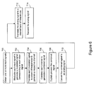
FIG. 6 , a flow chart of an example process for modulating and combining one or more channels is provided. Atblock 700, one or more input signals 614 are obtained by theGPU 16. In one embodiment, the input signals 614 can be provided by theFPGA 14 orCPU 18. In another embodiment, aninput signal 614 can be provided from thedemodulated signal 314 of theexample SDR device 10. - At
block 702, input signals 614 are modulated to generate a respective modulatedsignal 620. In the example SDR device 10' ofFIG. 5 , themodulation modules 318 of theGPU 16 modulate the input signals 614. In one embodiment, a plurality ofmodulation modules 318 operate in parallel to modulate multiple input signals 614 concurrently. - At
block 704, eachmodulated signal 620 is translated to a band of frequencies to generate arespective channel 320. In the example SDR device 10' ofFIG. 5 , thechannelizer modules 318 translate the modulatedsignals 620 to a band of frequencies. In an embodiment, eachmodulated signal 620 is translated to a different band of frequencies. In another embodiment, more than one modulatedsignal 620 can be translated to the same frequency. A plurality ofchannelizer modules 316 can operate in parallel. - At
block 706, eachchannel 320 is combined to generate a combinedsignal 622. In the example SDR device 10' ofFIG. 5 , amultiplexer 630 implemented on theFPGA 14 combines eachchannel 316 into the combinedsignal 622. - At
block 708, the combinedsignal 622 is digitally processed. In one embodiment, the combinedsignal 622 is prepared for improved digital to analog conversion. In the example SDR device 10' ofFIG. 5 , thedigital processing module 312 of theFPGA 14 digitally processes the combinedsignal 622. - At
block 710, the digital combinedsignal 622 is converted to ananalog signal 606. In the example SDR device 10' ofFIG. 5 , theDAC 604 of the RFfront end 12 performs the conversion. - At
block 712, theanalog signal 606 is translated to the desired band of frequencies. In the example SDR device 10' ofFIG. 5 , thepre-processing utility 302 of the RFfront end 12 performs the translation, using a centre frequency and filtering parameters provided by thetuning module 310 of the FPGA. 14. - At
block 714, theanalog signal 606 is transmitted. In the example SDR device 10' ofFIG. 5 , the transmitter 68 (e.g. an antenna) of the RF front end transmits theanalog signal 606. - An example application of the SDR device 10' of
FIG. 5 is to transmit audio data on multiple FM radio channels concurrently. For example, provided a song collection categorized into different genres, audio data of each genre can serve as aninput signal 614 to amodulation module 618 for frequency modulating the audio data of each genre on to a different channel. Themultiplexer 630 combines each channel into the combinedsignal 622 which is then be translated to a frequency band within the FM radio frequency band (i.e. 88.0 and 108.0 MHz) by thepre-processing utility 302 of the RFfront end 12. Theoutput signal 62 transmitted by the SDR device 10' contains audio data of each genre on separate FM radio channels that can be received by other FM radio devices. - In another example application, if each
input signal 614 corresponds to one frequency component of a signal, the SDR device 11 can combine the frequency components into the combinedsignal 622 to more accurately replicate the original signal because the combinedsignal 622 contains more frequency components than anindividual input signal 614. - As noted above, in one embodiment, the
input signal 614 of the example SDR device 10' can correspond to thedemodulated signal 314 of theexample SDR device 10. It can be appreciated that theSDR devices 10 and 10' can be implemented on a common RFfront end 12,FPGA 14,GPU 16 andCPU 18 to create one SDR device capable of performing the functionality of bothSDR devices 10 and 10'. It can also be appreciated that modules implemented on a component ofSDR devices 10 and 10' may be combined. - In one embodiment, a SDR device can intercept a
radio signal 22 havingmultiple channels 320 of information and demodulate eachchannel 320 according to a particular communication and demodulation protocol using the example process ofFIG. 5 . The same SDR device can then modulate and transmit eachdemodulated signal 314 according to a different communication and/or modulation protocol that does not correspond to the communication and/or modulation protocol of the channels in theradio signal 22 using the example process ofFIG. 7 . Example communication and modulation protocols that can be used include AM, SSB, Quadrature Amplitude modulation (QAM), GSM, Code Division Multiple Acces (CDMA), Global Packet Radio Service (GPRS), etc. - In this embodiment, the SDR device can translate information between different frequencies, modulation/demodulation protocols and/or communication protocols to allow communication between devices using different frequencies, modulation/demodulation protocols and/or communication protocols.
- For example, the SDR device can receive the
radio signal 22 containing information transmitted by a mobile device under a cellular communication protocol such as GSM or CDMA and rebroadcast the information over a different wireless network such as Wifi. In another embodiment, the radio signal can be translated and transmitted through a wired connection to a local area network (LAN). - Turning back to
FIGS. 2 and5 , theSDR devices 10 and 10' can also include aCPU 18 configured to provide auser interface 324 for allowing a user to interact with theSDR device 10. TheCPU 18 includes aGPU driver 326 and aFPGA driver 328. Thedrivers CPU 18 to communicate with theFPGA 14 and GPU 16 (for example, to program theFPGA 14 and GPU 16). - Turning to
FIG. 7 , a block diagram of aexample application layer 900 of theSDR device 10 is shown. In this example, theapplication layer 900 includes aSDR API 902 that provides the rules and specifications to access the components of thedevice 10, such asGPU 16 andFPGA 14. Each component also has its own driver to interface with the SDR API 902 (e.g. GPU driver 326, FPGA driver 328). Accordingly, a user can access thedevice 10 using theuser interface 324, which can include a command line interface (CLI) 904, web user interface (Web UI) 906 and/or graphical user interface (GUI) 908, enabling communication with the device resources through theAPI 902. In the example ofFIG. 7 , theAPI 902 can provide access to a local or remote memory 910 (e.g. remote memory can be accessible through a network). The local orremote memory 910 can store GPU programs and FPGA bit streams 912 used to operate theSDR device 10. - The
application layer 900 provides a common API to remote users connecting to theSDR device 10. The user can connect to the device for the purpose of receiving data from theSDR device 10, injecting data to be transmitted bySDR device 10, or for configuring theSDR device 10. It can be appreciated that thedevice 10 may be programmed to allow it to autonomously act to capture, transmit, store, or communicate with other devices. Theapplication layer 900 also provides a means by which processed data may be sent over another, possibly lower bandwidth, connection to remote users. Theapplication layer 900 can provide a mechanism by which remote users may access and retrieve stored data, as well as modify and program the behaviour of thedevice 10. - In one embodiment, the
Web UI 906 is operable to allow communication between theSDR device 10 and a remote user over the internet. For example, connections to theSDR device 10 can be made through an internet communication protocol such as Transmission Control Protocol / Internet Protocol (TCP/IP). A user can remotely communicate with theSDR device 10 using a third party web browser or SDR specific computer software. In the example of a web browser, GPU programs and FPGA bit streams 912 can be transferred over the network using a networking protocol such as Hypertext Transfer Protocol (HTTP) POST commands. TheWeb UI 906 can receive GPU programs and send them to theGPU 16 via theSDR API 902 andGPU driver 326. TheWeb UI 906 can receive FPGA bitstreams and send them to theFPGA 14 via theSDR API 902 and theFPGA driver 328. TheWeb UI 906 can also be operable to allow a user to configure and control the behaviour of theSDR device 10 through HTTP GET commands, for example. TheWeb UI 906 can translate the HTTP GET commands to API calls for theSDR API 902. - It can be appreciated that software running on the
SDR device 10 is not constrained to one physical component. It may run on theCPU 18,GPU 16,FPGA 14 and/or RFfront end 12. Each physical component can perform a different computational task. For example,CPU 18 orFPGA 14 can provide a user interface, retrieve and store data from memory, and dynamically program and configureGPU 16 and RFfront end 12. TheGPU 16 can run computationally intensive tasks such as spectrum analysis and cryptanalysis. The RFfront end 12 can provide the analog means necessary for a desired application. - It can also be appreciated that the
SDR 10 can perform management activities. This can include using the signal or spectral information to manage the connection or communication itself. Management activity can also include monitoring the network or ambient RF environment to modify the communication protocols parameters to optimize transmission, reception and other communication characteristics. TheSDR device 10 may be operable to redefine its transmission parameters independently, based on predefined algorithms or in concert with other devices. These cognitive algorithms may be calculated on theFPGA 14 or parallelized and calculated on theGPU 16. - Although the modules and components of the example configurations of the SDR device have been described with reference to specific embodiments that include an RF
front end 12,FPGA 14,GPU 16, andCPU 18, it will be appreciated that other embodiments are contemplated, including implementations on any suitable circuit comprising one or more circuit components or any suitable processing unit capable of performing the operations described. - Although the invention has been described with reference to certain specific embodiments, various modifications thereof will be apparent to those skilled in the art without departing from the scope of the invention as outlined in the claims appended hereto. The entire disclosures of all references recited above are incorporated herein by reference.
Claims (15)
- A method of extracting and demodulating one or more channels in a radio signal, the method comprising:receiving a first radio signal (22) using a radio frequency front end (12);translating a first band of frequencies of the first radio signal (22) to a second band of frequencies to generate a second radio signal;digitizing the second radio signal to generate a digital signal (306) containing a band of frequencies;improving or correcting errors introduced during said step of translating the first band of frequencies, by implementing a suitable digital up or down converter to translate the frequency band of the digital signal (306);extracting one or more additional band of frequencies of the digital signal (306), each additional band of frequencies corresponding to a channel (320); anddemodulating one or more channels (320) to generate a respective demodulated signal (314).
- The method of claim 1 wherein, in said step of translating the first band of frequencies, a band of frequencies are extracted from the radio signal (22) using said radio frequency front end (12) to generate a baseband signal, and wherein said step of digitizing the second radio signal is a step of digitizing said baseband signal, said errors being errors introduced during extraction of the desired band of frequencies by the radio frequency front end (12).
- The method of claim 1 or 2, wherein a plurality of additional band of frequencies of the digital signal (306) are extracted in parallel.
- The method of any one of claims 1 to 3, wherein a plurality of channels (320) are demodulated in parallel.
- The method of any one of claims 1 to 4 further comprising time domain averaging one or more demodulate signals (314), or frequency domain averaging one or more demodulated signals (314) with one or more other demodulated signals (314).
- The method of any one of claims 1 to 5 further comprising:modulating one or more of the demodulated signals (314, 614) to generate a respective modulated signal (620);translating a third band of frequencies of one or more modulated signals (620) to a fourth band of frequencies corresponding to an additional channel (320);combining one or more additional channels (320) to generate a combined signal (622);converting the combined signal (622) to an analog signal (606);translating a fifth band of frequencies of the analog signal (606) to a transmitting band of frequencies to generate a third radio signal (62); andtransmitting the third radio signal (62) using the radio frequency front end (12).
- The method of claim 6, wherein a plurality of demodulated signals (314, 614) are modulated in parallel, and optionally, a plurality of third band of frequencies are translated in parallel.
- The method of any one of claims 6 to 7, wherein one or more demodulated signals (314, 614) are modulated using a modulation technique that does not correspond to the demodulation technique used to demodulate the channel (320) corresponding to the demodulated signal (314).
- The method of any one of claims 6 to 8, wherein one or more channels (320) have a different communication protocol than its corresponding additional channel (320).
- A method of modulating and combining one or more channels into a radio signal, the method comprising:receiving one or more digital input signals (614);modulating one or more digital input signals (614) to generate a respective modulated signal (620);translating a first band of frequencies of one or more modulated signals (620) to a second band of frequencies corresponding to a channel (320);combining one or more channels (320) to generate a combined signal (622);preparing the combined signal (622) for improved digital to analog conversion by implementing a digital up and/or down converter;converting the combined signal to an analog signal (606);translating a third band of frequencies of the analog signal (606) to a transmitting band of frequencies to generate a radio signal (62); andtransmitting the radio signal (62) using a radio frequency front end (12).
- The method of claim 10, wherein a plurality digital input signals (614) are modulated in parallel, and optionally, a plurality of first band of frequencies are translated in parallel.
- An electronic device comprising a radio frequency front end (12), a processing unit and memory (13), the memory (13) storing computer executable instructions that when executed by the processing unit, causes the electronic device to perform the method of any one of claims 1 to 11.
- The electronic device of claim 12, wherein the processing unit comprises a field programmable gate array (14) in communication with the radio frequency front end (12), and optionally, the processing unit further comprises a graphics processing unit (16) in communication with the field programmable gate array (14) for performing parallel processing.
- The electronic device of claim 13 wherein at least one of the radio frequency front end (12), the field programmable gate array (14) and the graphics processing unit (16) is configured to receive data over a communication network, and optionally, the data includes configuration information for at least one of the radio frequency front end (12), the field programmable gate array (14) and the graphics processing unit (16).
- A computer readable storage medium (13) comprising computer executable instructions that when executed by a processing unit, causes the processing unit to perform the method of any one of claims 1 to 11.
Applications Claiming Priority (3)
| Application Number | Priority Date | Filing Date | Title |
|---|---|---|---|
| US201161532685P | 2011-09-09 | 2011-09-09 | |
| PCT/CA2012/000314 WO2012151662A1 (en) | 2011-05-06 | 2012-03-26 | System and method for decoding a radio signal |
| PCT/CA2012/050608 WO2013033840A1 (en) | 2011-09-09 | 2012-09-04 | Systems and methods for performing demodulation and modulation on software defined radios |
Publications (3)
| Publication Number | Publication Date |
|---|---|
| EP2754246A1 EP2754246A1 (en) | 2014-07-16 |
| EP2754246A4 EP2754246A4 (en) | 2015-05-20 |
| EP2754246B1 true EP2754246B1 (en) | 2016-06-22 |
Family
ID=47831402
Family Applications (1)
| Application Number | Title | Priority Date | Filing Date |
|---|---|---|---|
| EP12829337.0A Active EP2754246B1 (en) | 2011-09-09 | 2012-09-04 | Systems and methods for performing demodulation and modulation on software defined radios |
Country Status (4)
| Country | Link |
|---|---|
| US (1) | US9490750B2 (en) |
| EP (1) | EP2754246B1 (en) |
| ES (1) | ES2589278T3 (en) |
| WO (1) | WO2013033840A1 (en) |
Families Citing this family (7)
| Publication number | Priority date | Publication date | Assignee | Title |
|---|---|---|---|---|
| US9831898B2 (en) | 2013-03-13 | 2017-11-28 | Analog Devices Global | Radio frequency transmitter noise cancellation |
| EP2835926B1 (en) * | 2013-08-05 | 2019-06-12 | Alcatel Lucent | Transmitter apparatus for conditioning a multicarrier signal, network node, method for conditioning a multicarrier signal, and computer program thereof |
| US9912358B2 (en) | 2015-03-20 | 2018-03-06 | Analog Devices Global | Method of and apparatus for transmit noise reduction at a receiver |
| US10470063B2 (en) * | 2015-10-30 | 2019-11-05 | Afero, Inc. | Apparatus and method for capturing, manipulating, and analyzing wireless network traffic |
| US10289599B2 (en) * | 2016-10-15 | 2019-05-14 | Nxp Usa, Inc. | System and method employed for signal reception by providing programmable and switchable line terminations |
| DE102020213286A1 (en) * | 2020-10-21 | 2022-04-21 | Robert Bosch Gesellschaft mit beschränkter Haftung | Method for determining a phase position of a yaw rate signal or a quadrature signal, method for adapting a demodulation phase and yaw rate sensor |
| CN113890782B (en) * | 2021-09-24 | 2023-06-06 | 哈尔滨工程大学 | Software radio platform, method and device for loading task program |
Family Cites Families (31)
| Publication number | Priority date | Publication date | Assignee | Title |
|---|---|---|---|---|
| CA1187944A (en) | 1982-09-15 | 1985-05-28 | Her Majesty The Queen, In Right Of Canada, As Represented By The Ministe R Of National Defence | Spectrum surveillance receiver system |
| US4818949A (en) | 1988-01-06 | 1989-04-04 | U.S. Government As Represented By Director, National Security Agency | Microwave and millimeter-wave spectrum analyzer |
| US5289464A (en) * | 1992-09-21 | 1994-02-22 | At&T Bell Laboratories | Frequency-multiplexed cellular telephone cell site base station and method of operating the same |
| WO1997005705A1 (en) * | 1995-07-26 | 1997-02-13 | Telefonaktiebolaget Lm Ericsson (Publ) | Amps a-band single superhet |
| US6393046B1 (en) * | 1996-04-25 | 2002-05-21 | Sirf Technology, Inc. | Spread spectrum receiver with multi-bit correlator |
| US5812609A (en) | 1996-07-02 | 1998-09-22 | The United States Of America As Represented By The Secretary Of The National Security Agency | Communication intercept device using digital drop receivers in multiple tiers |
| US5999561A (en) * | 1997-05-20 | 1999-12-07 | Sanconix, Inc. | Direct sequence spread spectrum method, computer-based product, apparatus and system tolerant to frequency reference offset |
| US5970105A (en) * | 1998-05-11 | 1999-10-19 | Cleveland Medical Devices Inc. | Apparatus and method for efficient wireless communications in the presence of frequency error |
| SE9802059D0 (en) * | 1998-06-10 | 1998-06-10 | Ericsson Telefon Ab L M | Digital channeliser and De-shanneliser |
| US7110435B1 (en) * | 1999-03-15 | 2006-09-19 | Parkervision, Inc. | Spread spectrum applications of universal frequency translation |
| FR2791494B1 (en) * | 1999-03-23 | 2001-06-01 | France Telecom | BI-MODE RADIO FREQUENCY RECEIVING DEVICE AND CORRESPONDING MULTIMEDIA RECEIVER |
| US6166690A (en) * | 1999-07-02 | 2000-12-26 | Sensor Systems, Inc. | Adaptive nulling methods for GPS reception in multiple-interference environments |
| US6512803B2 (en) * | 2000-04-05 | 2003-01-28 | Symmetricom, Inc. | Global positioning system receiver capable of functioning in the presence of interference |
| US6931083B1 (en) * | 2000-05-26 | 2005-08-16 | Telasic Communications, Inc. | Low noise, low distortion, muxable Gilbert mixer signal processing system and method with AGC functionality |
| US7248841B2 (en) * | 2000-06-13 | 2007-07-24 | Agee Brian G | Method and apparatus for optimization of wireless multipoint electromagnetic communication networks |
| US6954614B2 (en) * | 2000-12-01 | 2005-10-11 | Lockheed Martin Corporation | Wideband transmission through narrowband transponder |
| US7236500B1 (en) | 2000-12-19 | 2007-06-26 | Intel Corporation | Demodulation of multi-user, multi-protocol data in a reconfigurable datapath |
| US7391819B1 (en) * | 2002-10-08 | 2008-06-24 | Urbain Alfred von der Embse | Capacity bound and modulation for communications |
| US7346134B2 (en) * | 2001-05-15 | 2008-03-18 | Finesse Wireless, Inc. | Radio receiver |
| KR100539230B1 (en) * | 2003-02-26 | 2005-12-27 | 삼성전자주식회사 | Physical layer unit providing for transmitting and receiving signals of several protocols, wireless Local Area Network system by the unit and wireless Local Area Network method |
| US20050118977A1 (en) * | 2003-12-02 | 2005-06-02 | Drogi Serge F. | Method, apparatus, and systems for digital radio communication systems |
| US20050141657A1 (en) * | 2003-12-30 | 2005-06-30 | Maltsev Alexander A. | Adaptive channel equalizer for wireless system |
| US7535978B2 (en) | 2004-04-02 | 2009-05-19 | Broadcom Corporation | Accurate signal detection in a wireless environment |
| US20070092045A1 (en) | 2005-10-21 | 2007-04-26 | Wangmyong Woo | Systems, Methods, and Apparatuses for Fine-Sensing Modules |
| US9654673B2 (en) | 2006-01-17 | 2017-05-16 | Koninklijke Philips N.V. | Detection of the presence of television signals embedded in noise using cyclostationary toolbox |
| US7443173B2 (en) * | 2006-06-19 | 2008-10-28 | Intel Corporation | Systems and techniques for radio frequency noise cancellation |
| US20080114247A1 (en) * | 2006-11-10 | 2008-05-15 | Penrith Corporation | Transducer array imaging system |
| KR100897158B1 (en) * | 2007-12-03 | 2009-05-14 | 한국전자통신연구원 | Multi-channel tuning receiver apparatus and multi-channel tuning method thereof |
| US20090323784A1 (en) | 2008-06-27 | 2009-12-31 | Microsoft Corporation | Software-Defined Radio Platform Based Upon Graphics Processing Unit |
| WO2010114167A1 (en) * | 2009-04-01 | 2010-10-07 | Nec Corporation | Channel estimation for a control channel in an ofdm system |
| US20120121036A1 (en) * | 2010-11-17 | 2012-05-17 | Cisco Technology, Inc. | Method and apparatus for clock spur suppression in direct-rf modulators |
-
2012
- 2012-09-04 WO PCT/CA2012/050608 patent/WO2013033840A1/en active Application Filing
- 2012-09-04 EP EP12829337.0A patent/EP2754246B1/en active Active
- 2012-09-04 ES ES12829337.0T patent/ES2589278T3/en active Active
-
2014
- 2014-03-06 US US14/199,805 patent/US9490750B2/en active Active
Also Published As
| Publication number | Publication date |
|---|---|
| EP2754246A4 (en) | 2015-05-20 |
| EP2754246A1 (en) | 2014-07-16 |
| US9490750B2 (en) | 2016-11-08 |
| ES2589278T3 (en) | 2016-11-11 |
| US20140185715A1 (en) | 2014-07-03 |
| WO2013033840A1 (en) | 2013-03-14 |
Similar Documents
| Publication | Publication Date | Title |
|---|---|---|
| US9490750B2 (en) | Systems and methods for performing demodulation and modulation on software defined radios | |
| US9992722B2 (en) | Reconfigurable multi-mode and multi-bands radio architecture and transceiver | |
| EP0766409B1 (en) | Multiband downconverter for digital receivers | |
| US8204537B2 (en) | Multiple frequency band information signal frequency band conversion | |
| US9680556B2 (en) | Narrowband signal transport sub-system for distributed antenna system | |
| US8412142B2 (en) | Multiple frequency band information signal universal front end with adjustable ADC(s) | |
| CN106134087A (en) | Spectrum-sensing radio receiver | |
| CN101116272A (en) | Communication apparatus | |
| US10211855B2 (en) | Apparatus for multi carrier aggregation in a software defined radio | |
| Chen et al. | Reconfigurable software defined radio and its applications | |
| US8798560B2 (en) | Multiple frequency band information signal universal front end with adjustable analog signal path components | |
| Meshram et al. | The advent software defined radio: FM receiver with RTL SDR and GNU radio | |
| CA2835035C (en) | System and method for decoding a radio signal | |
| US8385471B2 (en) | Multi-channel receiver | |
| US20100261435A1 (en) | Multiple frequency band information signal frequency band compression | |
| US8693307B2 (en) | Wireless communication system, transmitter, receiver and wireless communication method | |
| US8514785B2 (en) | Common RF interface for separating and mixing wireless signals | |
| WO2016149907A1 (en) | Receiver and signal processing method | |
| Yagoub et al. | Low cost sdr receiver implementation using rtl-sdr dongle | |
| CA2847969C (en) | Systems and methods for performing demodulation and modulation on software defined radios | |
| US20100261500A1 (en) | Multiple frequency band multiple standard information signal modular baseband processing module | |
| Somanaidu et al. | USRP 2901 based FM transceiver with large file capabilities in virtual and remote laboratory | |
| Dejonghe et al. | Versatile spectrum sensing on mobile devices? | |
| CN114846776B (en) | Wireless communication device and signal processing method | |
| Ugwuanyi et al. | Radio frequency and channel investigation using software defined radio in MATLAB And simulink environment |
Legal Events
| Date | Code | Title | Description |
|---|---|---|---|
| PUAI | Public reference made under article 153(3) epc to a published international application that has entered the european phase |
Free format text: ORIGINAL CODE: 0009012 |
|
| 17P | Request for examination filed |
Effective date: 20140408 |
|
| AK | Designated contracting states |
Kind code of ref document: A1 Designated state(s): AL AT BE BG CH CY CZ DE DK EE ES FI FR GB GR HR HU IE IS IT LI LT LU LV MC MK MT NL NO PL PT RO RS SE SI SK SM TR |
|
| DAX | Request for extension of the european patent (deleted) | ||
| RA4 | Supplementary search report drawn up and despatched (corrected) |
Effective date: 20150417 |
|
| RIC1 | Information provided on ipc code assigned before grant |
Ipc: H04B 7/14 20060101ALI20150413BHEP Ipc: H04B 1/50 20060101ALI20150413BHEP Ipc: H03D 9/00 20060101ALI20150413BHEP Ipc: H04L 27/00 20060101ALI20150413BHEP Ipc: H03J 1/00 20060101ALI20150413BHEP Ipc: H04B 1/16 20060101ALI20150413BHEP Ipc: H04B 1/00 20060101AFI20150413BHEP Ipc: H04W 16/14 20090101ALI20150413BHEP |
|
| GRAP | Despatch of communication of intention to grant a patent |
Free format text: ORIGINAL CODE: EPIDOSNIGR1 |
|
| INTG | Intention to grant announced |
Effective date: 20160115 |
|
| GRAS | Grant fee paid |
Free format text: ORIGINAL CODE: EPIDOSNIGR3 |
|
| GRAA | (expected) grant |
Free format text: ORIGINAL CODE: 0009210 |
|
| AK | Designated contracting states |
Kind code of ref document: B1 Designated state(s): AL AT BE BG CH CY CZ DE DK EE ES FI FR GB GR HR HU IE IS IT LI LT LU LV MC MK MT NL NO PL PT RO RS SE SI SK SM TR |
|
| REG | Reference to a national code |
Ref country code: GB Ref legal event code: FG4D |
|
| REG | Reference to a national code |
Ref country code: CH Ref legal event code: EP |
|
| REG | Reference to a national code |
Ref country code: IE Ref legal event code: FG4D |
|
| REG | Reference to a national code |
Ref country code: AT Ref legal event code: REF Ref document number: 808184 Country of ref document: AT Kind code of ref document: T Effective date: 20160715 |
|
| REG | Reference to a national code |
Ref country code: DE Ref legal event code: R096 Ref document number: 602012019844 Country of ref document: DE |
|
| REG | Reference to a national code |
Ref country code: CH Ref legal event code: NV Representative=s name: E. BLUM AND CO. AG PATENT- UND MARKENANWAELTE , CH |
|
| REG | Reference to a national code |
Ref country code: FR Ref legal event code: PLFP Year of fee payment: 5 |
|
| REG | Reference to a national code |
Ref country code: LT Ref legal event code: MG4D |
|
| REG | Reference to a national code |
Ref country code: NL Ref legal event code: MP Effective date: 20160622 |
|
| PG25 | Lapsed in a contracting state [announced via postgrant information from national office to epo] |
Ref country code: NO Free format text: LAPSE BECAUSE OF FAILURE TO SUBMIT A TRANSLATION OF THE DESCRIPTION OR TO PAY THE FEE WITHIN THE PRESCRIBED TIME-LIMIT Effective date: 20160922 Ref country code: LT Free format text: LAPSE BECAUSE OF FAILURE TO SUBMIT A TRANSLATION OF THE DESCRIPTION OR TO PAY THE FEE WITHIN THE PRESCRIBED TIME-LIMIT Effective date: 20160622 |
|
| REG | Reference to a national code |
Ref country code: ES Ref legal event code: FG2A Ref document number: 2589278 Country of ref document: ES Kind code of ref document: T3 Effective date: 20161111 |
|
| REG | Reference to a national code |
Ref country code: AT Ref legal event code: MK05 Ref document number: 808184 Country of ref document: AT Kind code of ref document: T Effective date: 20160622 |
|
| PG25 | Lapsed in a contracting state [announced via postgrant information from national office to epo] |
Ref country code: NL Free format text: LAPSE BECAUSE OF FAILURE TO SUBMIT A TRANSLATION OF THE DESCRIPTION OR TO PAY THE FEE WITHIN THE PRESCRIBED TIME-LIMIT Effective date: 20160622 Ref country code: HR Free format text: LAPSE BECAUSE OF FAILURE TO SUBMIT A TRANSLATION OF THE DESCRIPTION OR TO PAY THE FEE WITHIN THE PRESCRIBED TIME-LIMIT Effective date: 20160622 Ref country code: SE Free format text: LAPSE BECAUSE OF FAILURE TO SUBMIT A TRANSLATION OF THE DESCRIPTION OR TO PAY THE FEE WITHIN THE PRESCRIBED TIME-LIMIT Effective date: 20160622 Ref country code: LV Free format text: LAPSE BECAUSE OF FAILURE TO SUBMIT A TRANSLATION OF THE DESCRIPTION OR TO PAY THE FEE WITHIN THE PRESCRIBED TIME-LIMIT Effective date: 20160622 Ref country code: GR Free format text: LAPSE BECAUSE OF FAILURE TO SUBMIT A TRANSLATION OF THE DESCRIPTION OR TO PAY THE FEE WITHIN THE PRESCRIBED TIME-LIMIT Effective date: 20160923 Ref country code: RS Free format text: LAPSE BECAUSE OF FAILURE TO SUBMIT A TRANSLATION OF THE DESCRIPTION OR TO PAY THE FEE WITHIN THE PRESCRIBED TIME-LIMIT Effective date: 20160622 |
|
| PG25 | Lapsed in a contracting state [announced via postgrant information from national office to epo] |
Ref country code: RO Free format text: LAPSE BECAUSE OF FAILURE TO SUBMIT A TRANSLATION OF THE DESCRIPTION OR TO PAY THE FEE WITHIN THE PRESCRIBED TIME-LIMIT Effective date: 20160622 Ref country code: IS Free format text: LAPSE BECAUSE OF FAILURE TO SUBMIT A TRANSLATION OF THE DESCRIPTION OR TO PAY THE FEE WITHIN THE PRESCRIBED TIME-LIMIT Effective date: 20161022 Ref country code: SK Free format text: LAPSE BECAUSE OF FAILURE TO SUBMIT A TRANSLATION OF THE DESCRIPTION OR TO PAY THE FEE WITHIN THE PRESCRIBED TIME-LIMIT Effective date: 20160622 Ref country code: EE Free format text: LAPSE BECAUSE OF FAILURE TO SUBMIT A TRANSLATION OF THE DESCRIPTION OR TO PAY THE FEE WITHIN THE PRESCRIBED TIME-LIMIT Effective date: 20160622 Ref country code: CZ Free format text: LAPSE BECAUSE OF FAILURE TO SUBMIT A TRANSLATION OF THE DESCRIPTION OR TO PAY THE FEE WITHIN THE PRESCRIBED TIME-LIMIT Effective date: 20160622 |
|
| PG25 | Lapsed in a contracting state [announced via postgrant information from national office to epo] |
Ref country code: PT Free format text: LAPSE BECAUSE OF FAILURE TO SUBMIT A TRANSLATION OF THE DESCRIPTION OR TO PAY THE FEE WITHIN THE PRESCRIBED TIME-LIMIT Effective date: 20161024 Ref country code: BE Free format text: LAPSE BECAUSE OF NON-PAYMENT OF DUE FEES Effective date: 20160622 Ref country code: AT Free format text: LAPSE BECAUSE OF FAILURE TO SUBMIT A TRANSLATION OF THE DESCRIPTION OR TO PAY THE FEE WITHIN THE PRESCRIBED TIME-LIMIT Effective date: 20160622 Ref country code: SM Free format text: LAPSE BECAUSE OF FAILURE TO SUBMIT A TRANSLATION OF THE DESCRIPTION OR TO PAY THE FEE WITHIN THE PRESCRIBED TIME-LIMIT Effective date: 20160622 Ref country code: PL Free format text: LAPSE BECAUSE OF FAILURE TO SUBMIT A TRANSLATION OF THE DESCRIPTION OR TO PAY THE FEE WITHIN THE PRESCRIBED TIME-LIMIT Effective date: 20160622 |
|
| REG | Reference to a national code |
Ref country code: DE Ref legal event code: R097 Ref document number: 602012019844 Country of ref document: DE |
|
| PG25 | Lapsed in a contracting state [announced via postgrant information from national office to epo] |
Ref country code: MC Free format text: LAPSE BECAUSE OF FAILURE TO SUBMIT A TRANSLATION OF THE DESCRIPTION OR TO PAY THE FEE WITHIN THE PRESCRIBED TIME-LIMIT Effective date: 20160622 |
|
| PLBE | No opposition filed within time limit |
Free format text: ORIGINAL CODE: 0009261 |
|
| STAA | Information on the status of an ep patent application or granted ep patent |
Free format text: STATUS: NO OPPOSITION FILED WITHIN TIME LIMIT |
|
| 26N | No opposition filed |
Effective date: 20170323 |
|
| PG25 | Lapsed in a contracting state [announced via postgrant information from national office to epo] |
Ref country code: DK Free format text: LAPSE BECAUSE OF FAILURE TO SUBMIT A TRANSLATION OF THE DESCRIPTION OR TO PAY THE FEE WITHIN THE PRESCRIBED TIME-LIMIT Effective date: 20160622 |
|
| PG25 | Lapsed in a contracting state [announced via postgrant information from national office to epo] |
Ref country code: LU Free format text: LAPSE BECAUSE OF NON-PAYMENT OF DUE FEES Effective date: 20160904 Ref country code: SI Free format text: LAPSE BECAUSE OF FAILURE TO SUBMIT A TRANSLATION OF THE DESCRIPTION OR TO PAY THE FEE WITHIN THE PRESCRIBED TIME-LIMIT Effective date: 20160622 |
|
| REG | Reference to a national code |
Ref country code: FR Ref legal event code: PLFP Year of fee payment: 6 |
|
| PG25 | Lapsed in a contracting state [announced via postgrant information from national office to epo] |
Ref country code: HU Free format text: LAPSE BECAUSE OF FAILURE TO SUBMIT A TRANSLATION OF THE DESCRIPTION OR TO PAY THE FEE WITHIN THE PRESCRIBED TIME-LIMIT; INVALID AB INITIO Effective date: 20120904 |
|
| PG25 | Lapsed in a contracting state [announced via postgrant information from national office to epo] |
Ref country code: MK Free format text: LAPSE BECAUSE OF FAILURE TO SUBMIT A TRANSLATION OF THE DESCRIPTION OR TO PAY THE FEE WITHIN THE PRESCRIBED TIME-LIMIT Effective date: 20160622 Ref country code: MT Free format text: LAPSE BECAUSE OF NON-PAYMENT OF DUE FEES Effective date: 20160930 Ref country code: CY Free format text: LAPSE BECAUSE OF FAILURE TO SUBMIT A TRANSLATION OF THE DESCRIPTION OR TO PAY THE FEE WITHIN THE PRESCRIBED TIME-LIMIT Effective date: 20160622 |
|
| PG25 | Lapsed in a contracting state [announced via postgrant information from national office to epo] |
Ref country code: BG Free format text: LAPSE BECAUSE OF FAILURE TO SUBMIT A TRANSLATION OF THE DESCRIPTION OR TO PAY THE FEE WITHIN THE PRESCRIBED TIME-LIMIT Effective date: 20160622 |
|
| REG | Reference to a national code |
Ref country code: FR Ref legal event code: PLFP Year of fee payment: 7 |
|
| PG25 | Lapsed in a contracting state [announced via postgrant information from national office to epo] |
Ref country code: AL Free format text: LAPSE BECAUSE OF FAILURE TO SUBMIT A TRANSLATION OF THE DESCRIPTION OR TO PAY THE FEE WITHIN THE PRESCRIBED TIME-LIMIT Effective date: 20160622 Ref country code: TR Free format text: LAPSE BECAUSE OF FAILURE TO SUBMIT A TRANSLATION OF THE DESCRIPTION OR TO PAY THE FEE WITHIN THE PRESCRIBED TIME-LIMIT Effective date: 20160622 |
|
| PGFP | Annual fee paid to national office [announced via postgrant information from national office to epo] |
Ref country code: IT Payment date: 20230921 Year of fee payment: 12 Ref country code: IE Payment date: 20230927 Year of fee payment: 12 Ref country code: GB Payment date: 20230927 Year of fee payment: 12 Ref country code: FI Payment date: 20230925 Year of fee payment: 12 |
|
| PGFP | Annual fee paid to national office [announced via postgrant information from national office to epo] |
Ref country code: FR Payment date: 20230925 Year of fee payment: 12 Ref country code: DE Payment date: 20230927 Year of fee payment: 12 |
|
| PGFP | Annual fee paid to national office [announced via postgrant information from national office to epo] |
Ref country code: ES Payment date: 20231002 Year of fee payment: 12 |
|
| PGFP | Annual fee paid to national office [announced via postgrant information from national office to epo] |
Ref country code: CH Payment date: 20231004 Year of fee payment: 12 |