EP2736587B1 - Neural device with modular electrode array - Google Patents
Neural device with modular electrode array Download PDFInfo
- Publication number
- EP2736587B1 EP2736587B1 EP12751636.7A EP12751636A EP2736587B1 EP 2736587 B1 EP2736587 B1 EP 2736587B1 EP 12751636 A EP12751636 A EP 12751636A EP 2736587 B1 EP2736587 B1 EP 2736587B1
- Authority
- EP
- European Patent Office
- Prior art keywords
- conductive
- electrode
- electrodes
- modular
- flexible substrate
- Prior art date
- Legal status (The legal status is an assumption and is not a legal conclusion. Google has not performed a legal analysis and makes no representation as to the accuracy of the status listed.)
- Active
Links
- 230000001537 neural effect Effects 0.000 title claims description 58
- 239000000758 substrate Substances 0.000 claims description 24
- 230000000638 stimulation Effects 0.000 claims description 20
- 238000000034 method Methods 0.000 claims description 19
- 239000000463 material Substances 0.000 claims description 12
- 238000001746 injection moulding Methods 0.000 claims description 9
- 230000000149 penetrating effect Effects 0.000 claims description 8
- 229920001296 polysiloxane Polymers 0.000 claims description 8
- 239000010409 thin film Substances 0.000 claims description 8
- 238000000926 separation method Methods 0.000 claims description 5
- 238000012546 transfer Methods 0.000 claims description 4
- 238000010168 coupling process Methods 0.000 claims description 3
- 230000009467 reduction Effects 0.000 claims description 3
- 230000008878 coupling Effects 0.000 claims 2
- 238000005859 coupling reaction Methods 0.000 claims 2
- 210000001519 tissue Anatomy 0.000 description 24
- 238000004519 manufacturing process Methods 0.000 description 11
- 238000002566 electrocorticography Methods 0.000 description 10
- 210000004556 brain Anatomy 0.000 description 7
- 238000009413 insulation Methods 0.000 description 7
- 230000003287 optical effect Effects 0.000 description 7
- 230000000926 neurological effect Effects 0.000 description 6
- 238000003491 array Methods 0.000 description 5
- 239000000523 sample Substances 0.000 description 5
- 239000002131 composite material Substances 0.000 description 4
- 238000010586 diagram Methods 0.000 description 4
- 230000015654 memory Effects 0.000 description 4
- 210000002569 neuron Anatomy 0.000 description 4
- 230000008569 process Effects 0.000 description 4
- 239000004593 Epoxy Substances 0.000 description 3
- 238000004458 analytical method Methods 0.000 description 3
- 238000009826 distribution Methods 0.000 description 3
- 230000000694 effects Effects 0.000 description 3
- 230000006870 function Effects 0.000 description 3
- 238000013507 mapping Methods 0.000 description 3
- 238000012544 monitoring process Methods 0.000 description 3
- 241001465754 Metazoa Species 0.000 description 2
- 239000012530 fluid Substances 0.000 description 2
- 230000007774 longterm Effects 0.000 description 2
- 238000002595 magnetic resonance imaging Methods 0.000 description 2
- 238000005259 measurement Methods 0.000 description 2
- 210000000653 nervous system Anatomy 0.000 description 2
- 239000013307 optical fiber Substances 0.000 description 2
- 229920000307 polymer substrate Polymers 0.000 description 2
- 238000002271 resection Methods 0.000 description 2
- 239000003351 stiffener Substances 0.000 description 2
- 239000004642 Polyimide Substances 0.000 description 1
- 239000004830 Super Glue Substances 0.000 description 1
- 230000004913 activation Effects 0.000 description 1
- 239000000853 adhesive Substances 0.000 description 1
- 230000001070 adhesive effect Effects 0.000 description 1
- 210000003484 anatomy Anatomy 0.000 description 1
- 230000000712 assembly Effects 0.000 description 1
- 238000000429 assembly Methods 0.000 description 1
- 230000007175 bidirectional communication Effects 0.000 description 1
- 230000000975 bioactive effect Effects 0.000 description 1
- 239000000560 biocompatible material Substances 0.000 description 1
- 230000005540 biological transmission Effects 0.000 description 1
- 210000005013 brain tissue Anatomy 0.000 description 1
- 230000015556 catabolic process Effects 0.000 description 1
- 210000003710 cerebral cortex Anatomy 0.000 description 1
- 238000000576 coating method Methods 0.000 description 1
- 230000006854 communication Effects 0.000 description 1
- 238000004891 communication Methods 0.000 description 1
- 238000004590 computer program Methods 0.000 description 1
- 230000001054 cortical effect Effects 0.000 description 1
- 230000007585 cortical function Effects 0.000 description 1
- 238000007428 craniotomy Methods 0.000 description 1
- 238000006731 degradation reaction Methods 0.000 description 1
- 230000001419 dependent effect Effects 0.000 description 1
- 238000013461 design Methods 0.000 description 1
- 238000005516 engineering process Methods 0.000 description 1
- 206010015037 epilepsy Diseases 0.000 description 1
- 230000001037 epileptic effect Effects 0.000 description 1
- FGBJXOREULPLGL-UHFFFAOYSA-N ethyl cyanoacrylate Chemical compound CCOC(=O)C(=C)C#N FGBJXOREULPLGL-UHFFFAOYSA-N 0.000 description 1
- 230000001747 exhibiting effect Effects 0.000 description 1
- 238000001914 filtration Methods 0.000 description 1
- 229920005570 flexible polymer Polymers 0.000 description 1
- 238000002847 impedance measurement Methods 0.000 description 1
- 238000002347 injection Methods 0.000 description 1
- 239000007924 injection Substances 0.000 description 1
- 238000007689 inspection Methods 0.000 description 1
- 239000012774 insulation material Substances 0.000 description 1
- 230000001788 irregular Effects 0.000 description 1
- 230000007246 mechanism Effects 0.000 description 1
- 239000002184 metal Substances 0.000 description 1
- 238000000465 moulding Methods 0.000 description 1
- 210000003205 muscle Anatomy 0.000 description 1
- 230000000008 neuroelectric effect Effects 0.000 description 1
- 210000000578 peripheral nerve Anatomy 0.000 description 1
- 229920000052 poly(p-xylylene) Polymers 0.000 description 1
- 229920001721 polyimide Polymers 0.000 description 1
- 238000002360 preparation method Methods 0.000 description 1
- 238000012545 processing Methods 0.000 description 1
- 239000004065 semiconductor Substances 0.000 description 1
- 230000008054 signal transmission Effects 0.000 description 1
- 210000003625 skull Anatomy 0.000 description 1
- 210000000278 spinal cord Anatomy 0.000 description 1
- 230000003319 supportive effect Effects 0.000 description 1
- 238000001356 surgical procedure Methods 0.000 description 1
- 238000003466 welding Methods 0.000 description 1
Images


Classifications
-
- A—HUMAN NECESSITIES
- A61—MEDICAL OR VETERINARY SCIENCE; HYGIENE
- A61N—ELECTROTHERAPY; MAGNETOTHERAPY; RADIATION THERAPY; ULTRASOUND THERAPY
- A61N1/00—Electrotherapy; Circuits therefor
- A61N1/18—Applying electric currents by contact electrodes
- A61N1/32—Applying electric currents by contact electrodes alternating or intermittent currents
- A61N1/36—Applying electric currents by contact electrodes alternating or intermittent currents for stimulation
- A61N1/3605—Implantable neurostimulators for stimulating central or peripheral nerve system
- A61N1/3606—Implantable neurostimulators for stimulating central or peripheral nerve system adapted for a particular treatment
- A61N1/36064—Epilepsy
-
- A—HUMAN NECESSITIES
- A61—MEDICAL OR VETERINARY SCIENCE; HYGIENE
- A61B—DIAGNOSIS; SURGERY; IDENTIFICATION
- A61B5/00—Measuring for diagnostic purposes; Identification of persons
- A61B5/24—Detecting, measuring or recording bioelectric or biomagnetic signals of the body or parts thereof
-
- A—HUMAN NECESSITIES
- A61—MEDICAL OR VETERINARY SCIENCE; HYGIENE
- A61B—DIAGNOSIS; SURGERY; IDENTIFICATION
- A61B5/00—Measuring for diagnostic purposes; Identification of persons
- A61B5/24—Detecting, measuring or recording bioelectric or biomagnetic signals of the body or parts thereof
- A61B5/25—Bioelectric electrodes therefor
- A61B5/279—Bioelectric electrodes therefor specially adapted for particular uses
- A61B5/291—Bioelectric electrodes therefor specially adapted for particular uses for electroencephalography [EEG]
- A61B5/293—Invasive
-
- A—HUMAN NECESSITIES
- A61—MEDICAL OR VETERINARY SCIENCE; HYGIENE
- A61B—DIAGNOSIS; SURGERY; IDENTIFICATION
- A61B5/00—Measuring for diagnostic purposes; Identification of persons
- A61B5/40—Detecting, measuring or recording for evaluating the nervous system
- A61B5/4058—Detecting, measuring or recording for evaluating the nervous system for evaluating the central nervous system
- A61B5/4064—Evaluating the brain
-
- A—HUMAN NECESSITIES
- A61—MEDICAL OR VETERINARY SCIENCE; HYGIENE
- A61N—ELECTROTHERAPY; MAGNETOTHERAPY; RADIATION THERAPY; ULTRASOUND THERAPY
- A61N1/00—Electrotherapy; Circuits therefor
- A61N1/02—Details
- A61N1/04—Electrodes
- A61N1/05—Electrodes for implantation or insertion into the body, e.g. heart electrode
- A61N1/0526—Head electrodes
- A61N1/0529—Electrodes for brain stimulation
- A61N1/0531—Brain cortex electrodes
-
- A—HUMAN NECESSITIES
- A61—MEDICAL OR VETERINARY SCIENCE; HYGIENE
- A61N—ELECTROTHERAPY; MAGNETOTHERAPY; RADIATION THERAPY; ULTRASOUND THERAPY
- A61N5/00—Radiation therapy
- A61N5/06—Radiation therapy using light
-
- A—HUMAN NECESSITIES
- A61—MEDICAL OR VETERINARY SCIENCE; HYGIENE
- A61B—DIAGNOSIS; SURGERY; IDENTIFICATION
- A61B2562/00—Details of sensors; Constructional details of sensor housings or probes; Accessories for sensors
- A61B2562/04—Arrangements of multiple sensors of the same type
- A61B2562/046—Arrangements of multiple sensors of the same type in a matrix array
-
- A—HUMAN NECESSITIES
- A61—MEDICAL OR VETERINARY SCIENCE; HYGIENE
- A61B—DIAGNOSIS; SURGERY; IDENTIFICATION
- A61B5/00—Measuring for diagnostic purposes; Identification of persons
- A61B5/0059—Measuring for diagnostic purposes; Identification of persons using light, e.g. diagnosis by transillumination, diascopy, fluorescence
-
- A—HUMAN NECESSITIES
- A61—MEDICAL OR VETERINARY SCIENCE; HYGIENE
- A61B—DIAGNOSIS; SURGERY; IDENTIFICATION
- A61B5/00—Measuring for diagnostic purposes; Identification of persons
- A61B5/40—Detecting, measuring or recording for evaluating the nervous system
- A61B5/4076—Diagnosing or monitoring particular conditions of the nervous system
- A61B5/4094—Diagnosing or monitoring seizure diseases, e.g. epilepsy
-
- A—HUMAN NECESSITIES
- A61—MEDICAL OR VETERINARY SCIENCE; HYGIENE
- A61N—ELECTROTHERAPY; MAGNETOTHERAPY; RADIATION THERAPY; ULTRASOUND THERAPY
- A61N5/00—Radiation therapy
- A61N5/06—Radiation therapy using light
- A61N5/0613—Apparatus adapted for a specific treatment
- A61N5/0622—Optical stimulation for exciting neural tissue
-
- Y—GENERAL TAGGING OF NEW TECHNOLOGICAL DEVELOPMENTS; GENERAL TAGGING OF CROSS-SECTIONAL TECHNOLOGIES SPANNING OVER SEVERAL SECTIONS OF THE IPC; TECHNICAL SUBJECTS COVERED BY FORMER USPC CROSS-REFERENCE ART COLLECTIONS [XRACs] AND DIGESTS
- Y10—TECHNICAL SUBJECTS COVERED BY FORMER USPC
- Y10T—TECHNICAL SUBJECTS COVERED BY FORMER US CLASSIFICATION
- Y10T29/00—Metal working
- Y10T29/49—Method of mechanical manufacture
- Y10T29/49002—Electrical device making
- Y10T29/49117—Conductor or circuit manufacturing
Definitions
- This invention relates generally to the neural devices field, and more specifically to an improved neural device with modular electrode array in the neurotechnology field.
- Electrode array directly on the surface of the targeted neural tissue.
- the electrode array typically includes electrode sites that sense electrical activity in the tissue and can be used to assess neuronal activity.
- the electrode sites can also deliver small electrical currents to the tissue and can be used to stimulate neuronal activity.
- electrocorticography or ECoG
- ECoG involves placing an electrode array directly on the cerebral cortex, the outer surface of the brain.
- ECoG can be used in epilepsy mapping procedures conducted to identify and locate diseased tissue in preparation for surgical resection of the diseased tissue.
- conventional surface arrays are large and have a limited spatial resolution that reduces the precision of sensed electrical activity or stimulated electrical activity, resulting in reduced precision of gathered neural activity information or activation.
- This invention provides such an improved neural device.
- An implantable articulated electrode assembly may include an array of electrodes or electrical contacts carried by a support member configured to be implanted or positioned relative to a set of neuroanatomical sites.
- Various embodiments of the articulated electrode assemblies may comprise multiple portions, segments, paddles, and/or panels having spatially divergent placement capabilities in relation to one another. Such segments or panels may be positioned in a variety of manners relative to each other and/or one or more neuroanatomical sites or locations, which may facilitate establishment of an intended type of stimulation field distribution and/or monitoring configuration.
- WO 2011/067297 discloses microelectrode array devices, and methods of fabrication and use of the same, to provide highly localized and efficient electrical stimulation of a neurological target.
- the device includes multiple microelectrode elements arranged along a supportive backing layer.
- the microelectrode elements are dimensional and shaped so as to target individual neurons, groups of neurons, and neural tissue as may be located in an animal nervous system, such as along a region of a cortex of a human brain.
- the neurological probe can be used to facilitate location of the neurological target and remain implanted for long-term monitoring and/or stimulation.
- WO 2010/055421 discloses microelectrode array devices, and methods of fabrication and use of the same, to provide highly localized and efficient stimulation of a neurological target.
- the device includes multiple microelectrode elements arranged along an elongated probe shaft.
- the microelectrode elements are dimensioned and shaped so as to target individual neurons, groups of neurons, and neural tissue as may be located in an animal nervous system, such as deep within a human brain.
- the neurological probe can be used to facilitate location of the neurological target and remain implanted for long-term monitoring and/or stimulation.
- WO 2005/058145 discloses an electrode device for taking a plurality of EEG measurements, and an associated method of taking EEG measurements, whereby a plurality of electrode contact-points atop a support member are in electrical communication with, and in relative proximity to, an integrated circuit converter circuitry.
- the integrated circuit/circuitry may be supported by the support member or by a lead assembly having wiring for the digital signal transmission.
- the support member may have a plurality of layers and be generally flexible, as fabricated of any of a number of flexible, generally insulative biocompatible materials to which circuitry may be etched or deposited, exhibiting sufficient structural integrity to decrease likelihood of degradation during surgery or once implanted.
- the IC may further comprise circuitry for digital filtering and signal analysis of the digital signals.
- the neural interface can include an array having a plurality of micro-optrodes (HO).
- the micro-optrodes are capable of optical and electrical stimulation and recording, allowing bidirectional communication with neurotissue.
- At least a portion of the plurality of micro-optrodes are independently optically addressable and include an optical waveguide along each micro-optrode (HO).
- Combining optical stimulation with electrical recording can allow artifact-free recording from nearby electrodes and in some cases even the same electrode, which is difficult to achieve with combined electrical recording and stimulation.
- the optical waveguide is configured to direct light towards a distal end of the micro-optrode, allowing focal stimulation and recording. Penetrating micro-optrodes can allow access to deep tissue, while non-penetrating micro-optrodes can be used for extraneural stimulation.
- the invention provides an apparatus according to claim 1 and a method according to claim 10.
- Preferred embodiments are defined in the dependent claims. Examples, embodiments and aspects disclosed herein, but not falling under the scope of claim 1 or 10, do not form part of the invention.
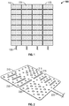
- FIGURE 1 shows an example of a neural device 100.
- the neural device 100 includes modular electrode array.
- the modular electrode array includes a modular flexible substrate.
- the modular flexible substrate includes a plurality of electrode modules 110.
- An electrode module 110 can be planar and can include a plurality of electrodes 115.
- the electrodes 115 may be configured to sense a neural signal at a neural source or deliver neural stimulation energy to a neural target.
- multiple signals can be sensed by a group or subset of the electrodes to form a composite signal.
- the group of electrodes used in sensing the composite signal can be called a macroelectrode and the individual electrodes can be called microelectrodes.
- the electrodes 115 can be called microelectrodes because of their small size.
- the modular flexible substrate can include a spatial separation between the electrode modules 110.
- the modular electrode array also includes conductive interconnect 120 (e.g., conductive traces or wires) coupled to the plurality of microelectrodes.
- the conductive interconnect 120 may be used to one or both of route electrical signals sensed by the electrodes and route stimulus signals to the electrodes.
- the interconnect 120 can be used to carry signals between modules or to carry signals between the modular electrode array and a device separate from the neural device 100.
- the modular flexible substrate may be supported by a backing 170 of flexible material, such as silicone or another flexible polymer.
- FIGURE 2 shows an example of an electrode module 210 that is planar.
- the electrode module 210 can include an array of microelectrodes 215 and can include one or more apertures 230.
- the apertures 230 may have different shapes, such as slots or circles as shown in the example.
- the electrode module 210 may be preformed to have a particular curvature in order to conform to known anatomy of the target tissue.
- the electrode module 210 can be a flexible thin-film microfabricated structure, such as a polymer substrate.
- the polymer substrate may be parylene or polyimide, but may additionally and/or alternatively include any suitable material. Layers of materials can be deposited on the substrate and patterned through microfabrication processes such as those used in manufacture of semiconductors.
- the flexible thin-film microfabricated structure may be supported by a backing of flexible material.
- the module may be made in any suitable manner.
- the microelectrodes 215 can be arranged in a microelectrode array of an approximately rectangular grid, although the microelectrodes 215 may include any number of microelectrodes 215 arranged in any suitable regular or irregular pattern.
- the microelectrode array can include recording electrodes that each provide a neural signal in a respective input channel, but additionally and/or alternatively may include stimulation or other kind of electrodes.
- the microelectrodes 215 can be elliptical.
- the microelectrodes 215 can be approximately circular, but the microelectrodes 215 may be any suitable shape.
- the electrode module 210 includes an array of microelectrodes that are substantially identical in size and shape.
- the electrode module 210 includes an array of microelectrodes that differ in one or both of shape and size.
- an electrode module 210 includes two substantially similar halves connected to each other. Each half including 32 microelectrodes (arranged in a 4 x 8 grid), such that each electrode module includes a total of 64 microelectrodes (arranged in an 8 x 8 grid) providing 64 channels of signal.
- the connected halves can be supported by a 1 mm thick silicone backing.
- the apertures 230 of the electrode module 210 may allow passage of a penetrating electrode (e.g. elongated electrode shank) to be placed within the tissue.
- a penetrating electrode e.g. elongated electrode shank
- one or more penetrating electrodes are included in the flexible substrate.
- a penetrating electrode includes a microelectrode array attached to a carrier, such as an insulated wire.
- the apertures 230 may allow release of brain fluid or other fluid from the tissue, and/or increase mechanical flexibility of the module.
- the apertures 230 may be elliptical holes (e.g. circular apertures to permit defined placement of cylindrical penetrating electrodes), slots, or any suitable shape, such as a custom shape configured to permit passage of a particular instrument through the module.
- the neural device may include one or more waveguides (e.g., an optical fiber) that delivers light to at least a portion of the one or more apertures.
- the apertures may form a series of ribs that increase the flexibility of a particular portion of the module.
- the apertures 230 may be interspersed between the microelectrodes 215 in a regular pattern.
- the electrode module 210 may not define any apertures and/or separate halves or other portions.
- the electrode modules can be combined to form a rectangular grid.
- the resulting rectangular grid can include microelectrodes that are distributed in a regular fashion within the rectangular grid.
- the modular electrode array includes 16 electrode modules arranged in four columns of four modules each.
- Each electrode module shown includes two connected portions including a total of 64 microelectrodes, such that the modular electrode array includes 1024 microelectrodes arranged in a regular 32 x 32 grid and providing 1024 channels of signal.
- the modular electrode array may include 32 modules arranged in an 8 x 4 grid, where each module includes 32 microelectrodes.
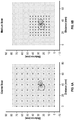
- FIGURES 3A and 3B illustrate a comparison of conventional electrode spacing ( FIGURE 3A ) and spacing using microelectrodes ( FIGURE 3B ).
- the spacing shown is for illustration purposes and is not meant to represent actual spacing of an actual device.
- the diameter of a microelectrode can be 0.575 millimeters (mm) and pitch between microelectrodes can be 2.5mm.
- the microelectrodes and the corresponding conductive traces coupled to the microelectrodes can be fabricated using microfabrication techniques to achieve the required spacing.
- Comparison of the FIGURES shows that an ECoG device having an array of 1024 microelectrodes takes up substantially the same area as an array of 64 conventional electrodes.
- an ECoG device having an array of microelectrodes includes more electrodes and conductive channels than a conventional 64-channel ECoG device.
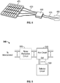
- FIGURE 4 shows an example of a system 400 that includes a neural device.
- the neural device includes a modular electrode array.
- the modular electrode array includes a modular flexible substrate that includes a plurality of electrode modules with a spatial separation between the electrode modules.
- a flexible backing 470 may support the modular flexible substrate.
- the electrode modules include electrodes and the modular electrode array includes conductive interconnect coupled to the electrodes.
- the system 400 also includes a plurality of electrically conductive leads 435 and an electronic subsystem 440 coupled to the electrically conductive leads 435 and the conductive interconnect of the modular electrode array.
- the conductive interconnect includes conductive traces 420 arranged to extend between the modular electrode array and the electronic subsystem 440.
- the number of electrical leads is less than the number of conductive traces.
- the electronic subsystem can include a multiplexer circuit to selectively transfer signals sensed by a subset of the plurality of conductive traces to one or more of the electrically conductive leads.
- FIGURE 5 shows a block diagram of an example of an electronic subsystem 540.
- the electronic subsystem 540 includes a multiplexer circuit 545 having signal inputs, select inputs, and one or more signal outputs.
- the signal inputs to the multiplexer circuit 545 can be electrically coupled to the conductive channels of the flexible substrate shown in FIGURE 4 .
- the electronic subsystem 540 also includes a selector circuit 550 electrically coupled to the select inputs of the multiplexer circuit and configured to activate the select inputs to direct a signal from an input of the multiplexer circuit to an output of the multiplexer circuit 545.
- the electronic subsystem can include a noise reduction circuit 555 (e.g., one or more filter circuits) to reduce signal noise.
- a noise reduction circuit 555 e.g., one or more filter circuits
- the system 400 can include a recording system 460 electrically coupled to the plurality of electrically conductive leads.
- the recording system 460 includes a data acquisition system (DAQ) that can include one or more of an analog to digital converter (ADC), a processor, and a memory.
- DAQ data acquisition system
- ADC analog to digital converter
- ADC analog to digital converter
- Multiplexing by the electronic subsystem 440 can reduce the number of recording channels needed in the recording system. Reducing the number of channels may enable the modular electrode array to be operable with a standard interface (e.g., conventional medical lead technologies having discrete wires). However, the electronic subsystem may interface with custom or other suitable lead systems.
- the electronic subsystem may lack a multiplexer such that the number of conductive traces (input channels) is equal to the number of leads coupled to the recording system, and/or may include other suitable front-end electronics, such as signal processing or noise reduction.
- the neural device may lack an electronic subsystem, such that the conductive traces also function as leads that directly couple the modular electrode array to the recording system.
- the conductive traces may be coupled to more durable leads more suitable for use external to the body, such as a ribbon cable.
- the modular electrode array of the neural device can include recording microelectrodes on the electrode modules that may be operable individually to record respective neural signals, and/or may be grouped in patterns of different sizes and/or shapes to emulate functionality of a macroelectrode.
- the neural device is selectively capable of sensing signals along a gradient of precision such that the user (e.g. neurologist) can "zoom" in on a particular area of tissue and sense from any number of the microelectrodes in a more precise manner, thereby gathering more detailed and “richer” information about the tissue.
- the neural device is also selectively capable of providing stimulation currents focused along a gradient of precision.
- the neural device can be used for electrocorticography (ECoG), such as in mapping brain tissue in an epileptic patient to more accurately and precisely identify and locate diseased tissue for surgical resection, or mapping cortical functions.
- EoG electrocorticography
- the neural device can be used for coverage of stimulation and/or recording of other tissue surfaces, such as those of the spinal cord, peripheral nerve, and/or muscle.
- the neural device may be used for any suitable neural recording and/or stimulation applications.
- the neural device uses the electrodes for impedance measurements, such as by using a first set of electrodes for applying a known current and a second set of electrodes to measure the voltage resulting from the applied current. Ohm's Law can then be used to determine the impedance of the tissue.
- the recording microelectrodes on the electrode modules may be operable individually to record respective neural signals, and/or may be grouped in patterns of different sizes and/or shapes to emulate functionality of a macroelectrode.
- a macroelectrode can be used to produce a composite signal that may be more appropriate for the desired analysis. Additionally, a composite signal can be interpreted as a signal from a conventional probe (e.g., a probe with a comparatively large electrode) allowing a user to perform similar analysis appropriate for conventional ECoG.
- a macroelectrode can also be used to stimulate a larger volume of tissue.
- the neural device can be selectively capable of sensing signals along a gradient of precision such that the user (e.g.
- a neurologist can "zoom" in on a particular area of tissue and sense signals from any number of the microelectrodes in a more precise manner, thereby gathering more detailed and “richer” information about the tissue.
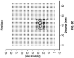
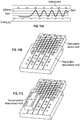
- the microelectrodes may be operated to scan in varying levels of resolution, such as by operation of the electronic subsystem 440 in FIGURE 4 . For instance, as shown in FIGURE 6A , in a coarse scan only a portion of the microelectrodes, loosely distributed across the tissue surface, are activated in a lower "resolution” of signal capture. In the coarse scan mode, a rough area of interest (e.g.
- dipole surface projection may identified and can be given closer inspection in a medium scan ( FIGURE 6B ), in which a more tightly distributed portion of the microelectrodes around the area of interest are activated.
- the area of interest may be even more closely analyzed in a fine scan mode ( FIGURE 6C ) that may activate all or nearly all of the nearby microelectrodes around that area.
- the resolution level of a scan may lie along any point in a gradient of resolution.
- the electrode modules may be specifically designed for particular functions and/or fits of targeted tissues.
- the thickness, footprint area shape, degree of flexibility, distribution or layout of microelectrodes, other module surface characteristics such as bioactive coatings, and/or any suitable characteristic of the module may be customized or specifically designed for a particular region or type of tissue, such as to conform closely with brain surfaces of gyrated brain (e.g. hugging crown of gyrus, following sulcus).
- this customizability of the modular electrode array also enables the neural device to be highly conformal and of a specialized design to conform to particular surface features.
- the interconnect functions to transfer signals to and from the modular electrode array.
- the interconnect can include conductive traces coupled to a respective module, and (as shown in FIGURE 7A ) conductive traces can be individually coupled to a microelectrode of the electrode module.
- the conductive traces may branch bilaterally symmetrically from the centerline of the electrode module.
- conductive traces can be arranged in a serpentine pattern, but may alternatively be arranged in any suitable manner.
- the flexible substrate may include a thin-film electrical signal filter (e.g., a low pass filter) microfabricated and conductively coupled to one or more of the conductive traces.
- FIGURE 8 shows an example of interconnect for a neural device.
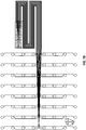
- the interconnect can include conductive traces 820 that can be gathered and helically coiled in groups, although the conductive traces 820 may alternatively be ungrouped and/or uncoiled.
- the spiral shape of the conductive traces 820 may reduce the electrical currents that are induced during magnetic resonance imaging (MRI), thereby making the neural device safe for use with MRI procedures that are often used to help place ECoG and other neural devices on target tissue.
- the coiled traces may be insulated with a flexible material (e.g., silicone).
- the conductive traces 820 may be coiled around a tube of flexible material.
- the interconnect may also include waveguides (e.g. thin-film waveguides, optical fibers) for guided light transmission in the device that can be used for optical stimulation or optical sensing of the tissue in the vicinity of the device.
- FIGURE 9 shows a flow diagram of an example of method 900 of manufacturing a neural device.
- Manufacturing the neural device includes manufacturing the modular electrode array and manufacturing the interconnect.
- electrode modules are formed.
- An electrode module includes a plurality of electrodes disposed on a planar module.
- the electrodes can be microelectrodes.
- One or more apertures can be formed in one or more of the electrode modules.
- the electrode modules may be manufactured using thin film microfabrication techniques.
- the individual electrode modules may include electrodes disposed on a planar flexible substrate and assembling the electrode modules may form a modular flexible substrate that includes the plurality of electrode modules and a spatial separation between adjoining electrode modules to form the modular electrode array.
- Manufacture of the neural device can include alignment and/or predictable relative positioning of the electrode modules in the modular electrode array.
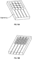
- manufacturing the modular electrode array can include laying the plurality of modules in an alignment jig, adhering the plurality of modules to one another, and injection molding a backing to the adhered modules.
- the jig can defines recesses, each receiving a respective module, and networked channels that join two or more recesses together.
- the jig can include a 4x4 rectangular grid for 16 modules, but may alternatively have any suitable number of recesses in other arrangements.
- the modular electrode array can include X rows of electrode modules and Y columns of electrode modules to an X by Y electrode array; where X and Y are positive integers.
- the respective interconnects can be gathered at one end and stacked in groups.
- Adhering the plurality of modules to one another can include applying epoxy to adjoining surfaces of the modules.
- the epoxy can be a UV-curable epoxy, but may be any suitable kind of adhesive.
- the modules may be joined with other coupling processes or mechanisms such as heat welding or with fasteners.
- the process can include attaching a backing to the modular flexible substrate.
- the backing can be attached by injection molding or adhering the backing to the modular flexible substrate.
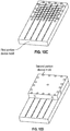
- Injection molding a backing to the adhered modules can include placing the adhered modules in a device mold, injecting backing material into the device mold, curing the backing material, and releasing modular electrode array from the device mold.
- the adhered modules can be placed in a first portion (e.g. bottom half) device mold and a second portion (e.g. top half) device mold can be aligned to the first portion device mold with pegs. After the first and second portion molds are clamped together, the backing material (e.g.
- silicone can be injected into the device mold and cured in an oven, thereby simultaneously forming the backing shape and adhering the backing material to the coupled modules. After curing, the device mold is opened and the backed modular electrode array is released.
- Other variations of the injection molding process may be used, such as those known and used by one ordinarily skilled in the art.
- conductive interconnect is formed and coupled to the electrodes at 915.
- the conductive interconnect can include conductive traces arranged in a serpentine pattern.
- the conductive traces can be separated and folded into a different arrangement (e.g., substantially straight).
- Interconnect can also be formed by grouping the conductive traces and helically coiling the grouped traces. Insulation can be injection molded around the coiled interconnect. At least a portion of the neural device may remain in the device mold during these steps.
- a group of conductive channels helically coiled or wrapped around a tube can be placed in a coiling jig that regulates the spacing and/or tension of the coiling.
- each group of conductive channels is preferably coiled separately. For instance, four different groups of traces may be coiled around four different tubes.
- Injection molding the insulation around the coiled conductive traces can be similar to the step of injection molding the backing of the modular electrode array and/or other injection molding processes.
- the coiled traces are preferably placed in a first portion (e.g. bottom half) interconnect mold and a second portion (e.g. top half) is aligned to the first portion interconnect mold with pegs.
- the insulation material e.g. silicone
- the insulation material is injected into the interconnect mold and cured in an oven, thereby simultaneously forming the insulation shape and adhering the insulation around the coiled interconnects.
- Each group of the coiled traces can be individually overmolded with insulation at separate times, although alternatively the coiled traces may simultaneously be overmolded with insulation.
- some portions of the device molds, coiling jig, and/or interconnect molds may be reused it multiple steps.
- a portion of the bottom half device mold may adapted to clamp to (1) the upper half device mold when injecting molding the backing of the modular electrode array, (2) the coiling jig when coiling the interconnects and (3) a portion of the bottom half interconnect mold when injection molding the insulation around the coiled interconnects.
- the device may alternatively be placed in separate molds and/or jigs for each step of the process.
- Method examples described herein can be machine or computer-implemented at least in part. Some examples can include a computer-readable medium or machine-readable medium encoded with instructions operable to configure an electronic device to perform methods as described in the above examples.
- An implementation of such methods can include code, such as microcode, assembly language code, a higher-level language code, or the like. Such code can include computer readable instructions for performing various methods. The code can form portions of computer program products. Further, the code can be tangibly stored on one or more volatile or non-volatile computer-readable media during execution or at other times.
- These computer-readable media can include, but are not limited to, hard disks, removable magnetic disks, removable optical disks (e.g., compact disks and digital video disks), magnetic cassettes, memory cards or sticks, random access memories (RAM's), read only memories (ROM's), and the like.
Landscapes
- Health & Medical Sciences (AREA)
- Life Sciences & Earth Sciences (AREA)
- Neurology (AREA)
- Engineering & Computer Science (AREA)
- Biomedical Technology (AREA)
- Animal Behavior & Ethology (AREA)
- General Health & Medical Sciences (AREA)
- Public Health (AREA)
- Veterinary Medicine (AREA)
- Neurosurgery (AREA)
- Heart & Thoracic Surgery (AREA)
- Pathology (AREA)
- Radiology & Medical Imaging (AREA)
- Nuclear Medicine, Radiotherapy & Molecular Imaging (AREA)
- Physics & Mathematics (AREA)
- Biophysics (AREA)
- Medical Informatics (AREA)
- Molecular Biology (AREA)
- Surgery (AREA)
- Psychology (AREA)
- Cardiology (AREA)
- Physiology (AREA)
- Measurement And Recording Of Electrical Phenomena And Electrical Characteristics Of The Living Body (AREA)
- Electrotherapy Devices (AREA)
- Solid State Image Pick-Up Elements (AREA)
Description
- This invention relates generally to the neural devices field, and more specifically to an improved neural device with modular electrode array in the neurotechnology field.
- Surface neural recording and stimulation involves placing an electrode array directly on the surface of the targeted neural tissue. The electrode array typically includes electrode sites that sense electrical activity in the tissue and can be used to assess neuronal activity. The electrode sites can also deliver small electrical currents to the tissue and can be used to stimulate neuronal activity. For example, electrocorticography, or ECoG, involves placing an electrode array directly on the cerebral cortex, the outer surface of the brain. ECoG can be used in epilepsy mapping procedures conducted to identify and locate diseased tissue in preparation for surgical resection of the diseased tissue. However, conventional surface arrays are large and have a limited spatial resolution that reduces the precision of sensed electrical activity or stimulated electrical activity, resulting in reduced precision of gathered neural activity information or activation. Thus, there is a need in the neural devices field to create an improved neural device with modular electrode arrays. This invention provides such an improved neural device.
- Reference is directed to
US 2010/0198297 which discloses subdural arrays that transmit electrocortiogram recordings wirelessly, across the patient's skull, allowing the craniotomy used for surgical placement of the arrays to be completely closed. In various embodiments, the arrays also respond to commands, applying signal patterns to the patient's brain for diagnostic and treatment purposes. - Reference is further directed to
US 2005/0154435 which discloses apparatus that may be configured for placement at one or more cortical and/or neuroanatomical sites to provide electrical stimulation and/or monitor neuroelectric activity within a patient. An implantable articulated electrode assembly may include an array of electrodes or electrical contacts carried by a support member configured to be implanted or positioned relative to a set of neuroanatomical sites. Various embodiments of the articulated electrode assemblies may comprise multiple portions, segments, paddles, and/or panels having spatially divergent placement capabilities in relation to one another. Such segments or panels may be positioned in a variety of manners relative to each other and/or one or more neuroanatomical sites or locations, which may facilitate establishment of an intended type of stimulation field distribution and/or monitoring configuration. - Reference is further directed to
WO 2011/067297 which discloses microelectrode array devices, and methods of fabrication and use of the same, to provide highly localized and efficient electrical stimulation of a neurological target. The device includes multiple microelectrode elements arranged along a supportive backing layer. The microelectrode elements are dimensional and shaped so as to target individual neurons, groups of neurons, and neural tissue as may be located in an animal nervous system, such as along a region of a cortex of a human brain. Beneficially, the neurological probe can be used to facilitate location of the neurological target and remain implanted for long-term monitoring and/or stimulation. - Reference is further directed to
WO 2010/055421 which discloses microelectrode array devices, and methods of fabrication and use of the same, to provide highly localized and efficient stimulation of a neurological target. The device includes multiple microelectrode elements arranged along an elongated probe shaft. The microelectrode elements are dimensioned and shaped so as to target individual neurons, groups of neurons, and neural tissue as may be located in an animal nervous system, such as deep within a human brain. Beneficially, the neurological probe can be used to facilitate location of the neurological target and remain implanted for long-term monitoring and/or stimulation. - Reference is further directed to
WO 2005/058145 which discloses an electrode device for taking a plurality of EEG measurements, and an associated method of taking EEG measurements, whereby a plurality of electrode contact-points atop a support member are in electrical communication with, and in relative proximity to, an integrated circuit converter circuitry. The integrated circuit/circuitry (IC) may be supported by the support member or by a lead assembly having wiring for the digital signal transmission. The support member may have a plurality of layers and be generally flexible, as fabricated of any of a number of flexible, generally insulative biocompatible materials to which circuitry may be etched or deposited, exhibiting sufficient structural integrity to decrease likelihood of degradation during surgery or once implanted. The IC may further comprise circuitry for digital filtering and signal analysis of the digital signals. - Reference is further directed to
WO 2011/057276 which discloses a hybrid optical-electrical neural interface. The neural interface can include an array having a plurality of micro-optrodes (HO). The micro-optrodes are capable of optical and electrical stimulation and recording, allowing bidirectional communication with neurotissue. At least a portion of the plurality of micro-optrodes are independently optically addressable and include an optical waveguide along each micro-optrode (HO). Combining optical stimulation with electrical recording can allow artifact-free recording from nearby electrodes and in some cases even the same electrode, which is difficult to achieve with combined electrical recording and stimulation. The optical waveguide is configured to direct light towards a distal end of the micro-optrode, allowing focal stimulation and recording. Penetrating micro-optrodes can allow access to deep tissue, while non-penetrating micro-optrodes can be used for extraneural stimulation. - The invention provides an apparatus according to
claim 1 and a method according toclaim 10. Preferred embodiments are defined in the dependent claims. Examples, embodiments and aspects disclosed herein, but not falling under the scope ofclaim -
-
FIGURE 1 is a schematic of an example of a neural device, consistent with some example embodiments of the invention. -
FIGURE 2 is a detailed schematic of an example of an electrode module in the modular electrode array in a neural device, consistent with some example embodiments of the invention. -
FIGURES 3A and 3B show a comparison of the microelectrode distribution between a conventional ECoG device and an example of a neural device consistent with some example embodiments of the invention, respectively. -
FIGURE 4 is a schematic of an example of a neural device, consistent with some example embodiments of the invention. -
FIGURE 5 shows a block diagram of portions of an example of an electronic subsystem. -
FIGURES 6A-6C is an illustration of an example of multi-scale functionality of a neural device consistent with some example embodiments of the invention. -
FIGURES 7A and7B show detailed schematics of examples of interconnects in a neural device of a preferred embodiment; -
FIGURE 8 is a schematic of an example of coiled interconnects in a neural device, consistent with some example embodiments of the invention. -
FIGURE 9 shows a flow diagram of an example of method of manufacturing a neural device. -
FIGURES 10A-D and11A-C illustrate an example of a method of manufacturing and assembling a neural device, consistent with some example embodiments of the invention. - The following description of example embodiments of the invention is not intended to limit the invention to these embodiments, but rather to enable any person skilled in the art to make and use this invention.
-
FIGURE 1 shows an example of aneural device 100. Theneural device 100 includes modular electrode array. The modular electrode array includes a modular flexible substrate. The modular flexible substrate includes a plurality ofelectrode modules 110. Anelectrode module 110 can be planar and can include a plurality ofelectrodes 115. Theelectrodes 115 may be configured to sense a neural signal at a neural source or deliver neural stimulation energy to a neural target. As is described herein, multiple signals can be sensed by a group or subset of the electrodes to form a composite signal. The group of electrodes used in sensing the composite signal can be called a macroelectrode and the individual electrodes can be called microelectrodes. Theelectrodes 115 can be called microelectrodes because of their small size. The modular flexible substrate can include a spatial separation between theelectrode modules 110. The modular electrode array also includes conductive interconnect 120 (e.g., conductive traces or wires) coupled to the plurality of microelectrodes. Theconductive interconnect 120 may be used to one or both of route electrical signals sensed by the electrodes and route stimulus signals to the electrodes. Theinterconnect 120 can be used to carry signals between modules or to carry signals between the modular electrode array and a device separate from theneural device 100. The modular flexible substrate may be supported by abacking 170 of flexible material, such as silicone or another flexible polymer. -
FIGURE 2 shows an example of anelectrode module 210 that is planar. Theelectrode module 210 can include an array ofmicroelectrodes 215 and can include one ormore apertures 230. Theapertures 230 may have different shapes, such as slots or circles as shown in the example. In some variations, theelectrode module 210 may be preformed to have a particular curvature in order to conform to known anatomy of the target tissue. Theelectrode module 210 can be a flexible thin-film microfabricated structure, such as a polymer substrate. The polymer substrate may be parylene or polyimide, but may additionally and/or alternatively include any suitable material. Layers of materials can be deposited on the substrate and patterned through microfabrication processes such as those used in manufacture of semiconductors. The flexible thin-film microfabricated structure may be supported by a backing of flexible material. However, the module may be made in any suitable manner. - The
microelectrodes 215 can be arranged in a microelectrode array of an approximately rectangular grid, although themicroelectrodes 215 may include any number ofmicroelectrodes 215 arranged in any suitable regular or irregular pattern. The microelectrode array can include recording electrodes that each provide a neural signal in a respective input channel, but additionally and/or alternatively may include stimulation or other kind of electrodes. In certain variations themicroelectrodes 215 can be elliptical. In certain variations, themicroelectrodes 215 can be approximately circular, but themicroelectrodes 215 may be any suitable shape. In some examples, theelectrode module 210 includes an array of microelectrodes that are substantially identical in size and shape. In some examples, theelectrode module 210 includes an array of microelectrodes that differ in one or both of shape and size. In an illustrative non-limiting example, anelectrode module 210 includes two substantially similar halves connected to each other. Each half including 32 microelectrodes (arranged in a 4 x 8 grid), such that each electrode module includes a total of 64 microelectrodes (arranged in an 8 x 8 grid) providing 64 channels of signal. The connected halves can be supported by a 1 mm thick silicone backing. - The
apertures 230 of theelectrode module 210 may allow passage of a penetrating electrode (e.g. elongated electrode shank) to be placed within the tissue. In some examples, one or more penetrating electrodes are included in the flexible substrate. In some examples, a penetrating electrode includes a microelectrode array attached to a carrier, such as an insulated wire. Theapertures 230 may allow release of brain fluid or other fluid from the tissue, and/or increase mechanical flexibility of the module. As shown inFIGURE 2 , theapertures 230 may be elliptical holes (e.g. circular apertures to permit defined placement of cylindrical penetrating electrodes), slots, or any suitable shape, such as a custom shape configured to permit passage of a particular instrument through the module. The neural device may include one or more waveguides (e.g., an optical fiber) that delivers light to at least a portion of the one or more apertures. In some variations, the apertures may form a series of ribs that increase the flexibility of a particular portion of the module. Theapertures 230 may be interspersed between themicroelectrodes 215 in a regular pattern. Alternatively, theelectrode module 210 may not define any apertures and/or separate halves or other portions. - Multiple electrode modules can be combined to form the modular electrode array. The electrode modules may be combined to form a rectangular grid. The resulting rectangular grid can include microelectrodes that are distributed in a regular fashion within the rectangular grid. For example, as shown in
FIGURE 1 , the modular electrode array includes 16 electrode modules arranged in four columns of four modules each. Each electrode module shown includes two connected portions including a total of 64 microelectrodes, such that the modular electrode array includes 1024 microelectrodes arranged in a regular 32 x 32 grid and providing 1024 channels of signal. In an alternative arrangement providing a similar layout of 1024 microelectrodes, the modular electrode array may include 32 modules arranged in an 8 x 4 grid, where each module includes 32 microelectrodes. -
FIGURES 3A and 3B illustrate a comparison of conventional electrode spacing (FIGURE 3A ) and spacing using microelectrodes (FIGURE 3B ). The spacing shown is for illustration purposes and is not meant to represent actual spacing of an actual device. In a non-limiting example, the diameter of a microelectrode can be 0.575 millimeters (mm) and pitch between microelectrodes can be 2.5mm. The microelectrodes and the corresponding conductive traces coupled to the microelectrodes can be fabricated using microfabrication techniques to achieve the required spacing. Comparison of the FIGURES shows that an ECoG device having an array of 1024 microelectrodes takes up substantially the same area as an array of 64 conventional electrodes. Thus, an ECoG device having an array of microelectrodes includes more electrodes and conductive channels than a conventional 64-channel ECoG device. -
FIGURE 4 shows an example of a system 400 that includes a neural device. The neural device includes a modular electrode array. The modular electrode array includes a modular flexible substrate that includes a plurality of electrode modules with a spatial separation between the electrode modules. Aflexible backing 470 may support the modular flexible substrate. The electrode modules include electrodes and the modular electrode array includes conductive interconnect coupled to the electrodes. The system 400 also includes a plurality of electrically conductive leads 435 and anelectronic subsystem 440 coupled to the electrically conductive leads 435 and the conductive interconnect of the modular electrode array. In some examples, the conductive interconnect includesconductive traces 420 arranged to extend between the modular electrode array and theelectronic subsystem 440. In some examples, the number of electrical leads is less than the number of conductive traces. The electronic subsystem can include a multiplexer circuit to selectively transfer signals sensed by a subset of the plurality of conductive traces to one or more of the electrically conductive leads. -
FIGURE 5 shows a block diagram of an example of anelectronic subsystem 540. Theelectronic subsystem 540 includes amultiplexer circuit 545 having signal inputs, select inputs, and one or more signal outputs. The signal inputs to themultiplexer circuit 545 can be electrically coupled to the conductive channels of the flexible substrate shown inFIGURE 4 . Theelectronic subsystem 540 also includes aselector circuit 550 electrically coupled to the select inputs of the multiplexer circuit and configured to activate the select inputs to direct a signal from an input of the multiplexer circuit to an output of themultiplexer circuit 545. In some variations, the electronic subsystem can include a noise reduction circuit 555 (e.g., one or more filter circuits) to reduce signal noise. - Returning to
FIGURE 4 , the system 400 can include arecording system 460 electrically coupled to the plurality of electrically conductive leads. In certain examples, therecording system 460 includes a data acquisition system (DAQ) that can include one or more of an analog to digital converter (ADC), a processor, and a memory. Multiplexing by theelectronic subsystem 440 can reduce the number of recording channels needed in the recording system. Reducing the number of channels may enable the modular electrode array to be operable with a standard interface (e.g., conventional medical lead technologies having discrete wires). However, the electronic subsystem may interface with custom or other suitable lead systems. In some variations, the electronic subsystem may lack a multiplexer such that the number of conductive traces (input channels) is equal to the number of leads coupled to the recording system, and/or may include other suitable front-end electronics, such as signal processing or noise reduction. Alternatively, the neural device may lack an electronic subsystem, such that the conductive traces also function as leads that directly couple the modular electrode array to the recording system. In this alternative, the conductive traces may be coupled to more durable leads more suitable for use external to the body, such as a ribbon cable. - The modular electrode array of the neural device can include recording microelectrodes on the electrode modules that may be operable individually to record respective neural signals, and/or may be grouped in patterns of different sizes and/or shapes to emulate functionality of a macroelectrode. The neural device is selectively capable of sensing signals along a gradient of precision such that the user (e.g. neurologist) can "zoom" in on a particular area of tissue and sense from any number of the microelectrodes in a more precise manner, thereby gathering more detailed and "richer" information about the tissue. The neural device is also selectively capable of providing stimulation currents focused along a gradient of precision. The neural device can be used for electrocorticography (ECoG), such as in mapping brain tissue in an epileptic patient to more accurately and precisely identify and locate diseased tissue for surgical resection, or mapping cortical functions. In some embodiments, the neural device can be used for coverage of stimulation and/or recording of other tissue surfaces, such as those of the spinal cord, peripheral nerve, and/or muscle. However, the neural device may be used for any suitable neural recording and/or stimulation applications. In certain variations, the neural device uses the electrodes for impedance measurements, such as by using a first set of electrodes for applying a known current and a second set of electrodes to measure the voltage resulting from the applied current. Ohm's Law can then be used to determine the impedance of the tissue.
- The recording microelectrodes on the electrode modules may be operable individually to record respective neural signals, and/or may be grouped in patterns of different sizes and/or shapes to emulate functionality of a macroelectrode. A macroelectrode can be used to produce a composite signal that may be more appropriate for the desired analysis. Additionally, a composite signal can be interpreted as a signal from a conventional probe (e.g., a probe with a comparatively large electrode) allowing a user to perform similar analysis appropriate for conventional ECoG. A macroelectrode can also be used to stimulate a larger volume of tissue. Furthermore, the neural device can be selectively capable of sensing signals along a gradient of precision such that the user (e.g. a neurologist) can "zoom" in on a particular area of tissue and sense signals from any number of the microelectrodes in a more precise manner, thereby gathering more detailed and "richer" information about the tissue. The microelectrodes may be operated to scan in varying levels of resolution, such as by operation of the
electronic subsystem 440 inFIGURE 4 . For instance, as shown inFIGURE 6A , in a coarse scan only a portion of the microelectrodes, loosely distributed across the tissue surface, are activated in a lower "resolution" of signal capture. In the coarse scan mode, a rough area of interest (e.g. dipole surface projection) may identified and can be given closer inspection in a medium scan (FIGURE 6B ), in which a more tightly distributed portion of the microelectrodes around the area of interest are activated. The area of interest may be even more closely analyzed in a fine scan mode (FIGURE 6C ) that may activate all or nearly all of the nearby microelectrodes around that area. The resolution level of a scan may lie along any point in a gradient of resolution. - In some embodiments, at least a portion of the electrode modules may be specifically designed for particular functions and/or fits of targeted tissues. For instance, the thickness, footprint area shape, degree of flexibility, distribution or layout of microelectrodes, other module surface characteristics such as bioactive coatings, and/or any suitable characteristic of the module may be customized or specifically designed for a particular region or type of tissue, such as to conform closely with brain surfaces of gyrated brain (e.g. hugging crown of gyrus, following sulcus). In other words, this customizability of the modular electrode array also enables the neural device to be highly conformal and of a specialized design to conform to particular surface features.
- The interconnect functions to transfer signals to and from the modular electrode array. The interconnect can include conductive traces coupled to a respective module, and (as shown in
FIGURE 7A ) conductive traces can be individually coupled to a microelectrode of the electrode module. The conductive traces may branch bilaterally symmetrically from the centerline of the electrode module. As shown inFIGURE 7B , relative to each electrode module, conductive traces can be arranged in a serpentine pattern, but may alternatively be arranged in any suitable manner. The flexible substrate may include a thin-film electrical signal filter (e.g., a low pass filter) microfabricated and conductively coupled to one or more of the conductive traces. -
FIGURE 8 shows an example of interconnect for a neural device. The interconnect can includeconductive traces 820 that can be gathered and helically coiled in groups, although theconductive traces 820 may alternatively be ungrouped and/or uncoiled. The spiral shape of theconductive traces 820 may reduce the electrical currents that are induced during magnetic resonance imaging (MRI), thereby making the neural device safe for use with MRI procedures that are often used to help place ECoG and other neural devices on target tissue. The coiled traces may be insulated with a flexible material (e.g., silicone). The conductive traces 820 may be coiled around a tube of flexible material. The interconnect may also include waveguides (e.g. thin-film waveguides, optical fibers) for guided light transmission in the device that can be used for optical stimulation or optical sensing of the tissue in the vicinity of the device. -
FIGURE 9 shows a flow diagram of an example ofmethod 900 of manufacturing a neural device. Manufacturing the neural device includes manufacturing the modular electrode array and manufacturing the interconnect. Atblock 905, electrode modules are formed. An electrode module includes a plurality of electrodes disposed on a planar module. The electrodes can be microelectrodes. One or more apertures can be formed in one or more of the electrode modules. The electrode modules may be manufactured using thin film microfabrication techniques. - At
block 910, multiple electrode modules are assembled into a modular electrode array. The individual electrode modules may include electrodes disposed on a planar flexible substrate and assembling the electrode modules may form a modular flexible substrate that includes the plurality of electrode modules and a spatial separation between adjoining electrode modules to form the modular electrode array. Manufacture of the neural device can include alignment and/or predictable relative positioning of the electrode modules in the modular electrode array. As shown inFIGURES 10A and 10B , manufacturing the modular electrode array can include laying the plurality of modules in an alignment jig, adhering the plurality of modules to one another, and injection molding a backing to the adhered modules. The jig can defines recesses, each receiving a respective module, and networked channels that join two or more recesses together. The jig can include a 4x4 rectangular grid for 16 modules, but may alternatively have any suitable number of recesses in other arrangements. For the general case, the modular electrode array can include X rows of electrode modules and Y columns of electrode modules to an X by Y electrode array; where X and Y are positive integers. In laying the modules in respective recesses, the respective interconnects can be gathered at one end and stacked in groups. Adhering the plurality of modules to one another can include applying epoxy to adjoining surfaces of the modules. The epoxy can be a UV-curable epoxy, but may be any suitable kind of adhesive. Alternatively, the modules may be joined with other coupling processes or mechanisms such as heat welding or with fasteners. - The process can include attaching a backing to the modular flexible substrate. The backing can be attached by injection molding or adhering the backing to the modular flexible substrate. Injection molding a backing to the adhered modules can include placing the adhered modules in a device mold, injecting backing material into the device mold, curing the backing material, and releasing modular electrode array from the device mold. As shown in
FIGURES 10C and 10D , the adhered modules can be placed in a first portion (e.g. bottom half) device mold and a second portion (e.g. top half) device mold can be aligned to the first portion device mold with pegs. After the first and second portion molds are clamped together, the backing material (e.g. silicone) can be injected into the device mold and cured in an oven, thereby simultaneously forming the backing shape and adhering the backing material to the coupled modules. After curing, the device mold is opened and the backed modular electrode array is released. Other variations of the injection molding process may be used, such as those known and used by one ordinarily skilled in the art. - Returning to
FIGURE 9 , conductive interconnect is formed and coupled to the electrodes at 915. The conductive interconnect can include conductive traces arranged in a serpentine pattern. The conductive traces can be separated and folded into a different arrangement (e.g., substantially straight). Interconnect can also be formed by grouping the conductive traces and helically coiling the grouped traces. Insulation can be injection molded around the coiled interconnect. At least a portion of the neural device may remain in the device mold during these steps. As shown inFIGURE 11A , a group of conductive channels helically coiled or wrapped around a tube can be placed in a coiling jig that regulates the spacing and/or tension of the coiling. During coiling, portions of the traces may be periodically tacked to the tube (e.g., with cyanoacrylate adhesive) to prevent uncoiling. The tube can be made of a flexible material such as silicone, and may include a stiffener such as a metal wire inserted in a lumen of the tube, to increase rigidity of the tube during coiling of the lead. The stiffener may or may not be removed from the tube after coiling. In some examples, each group of conductive channels is preferably coiled separately. For instance, four different groups of traces may be coiled around four different tubes. - Injection molding the insulation around the coiled conductive traces can be similar to the step of injection molding the backing of the modular electrode array and/or other injection molding processes. As shown in
FIGURES 11B and 11C , the coiled traces are preferably placed in a first portion (e.g. bottom half) interconnect mold and a second portion (e.g. top half) is aligned to the first portion interconnect mold with pegs. After the first and second portion interconnect molds are clamped together, the insulation material (e.g. silicone) is injected into the interconnect mold and cured in an oven, thereby simultaneously forming the insulation shape and adhering the insulation around the coiled interconnects. Each group of the coiled traces can be individually overmolded with insulation at separate times, although alternatively the coiled traces may simultaneously be overmolded with insulation. - In some embodiments, some portions of the device molds, coiling jig, and/or interconnect molds may be reused it multiple steps. For instance, a portion of the bottom half device mold may adapted to clamp to (1) the upper half device mold when injecting molding the backing of the modular electrode array, (2) the coiling jig when coiling the interconnects and (3) a portion of the bottom half interconnect mold when injection molding the insulation around the coiled interconnects. However, the device may alternatively be placed in separate molds and/or jigs for each step of the process.
- The above detailed description includes references to the accompanying drawings, which form a part of the detailed description. The drawings show, by way of illustration, specific embodiments in which the invention can be practiced. These embodiments are also referred to herein as "examples."
- In this document, the terms "a" or "an" are used, as is common in patent documents, to include one or more than one, independent of any other instances or usages of "at least one" or "one or more." In this document, the term "or" is used to refer to a nonexclusive or, such that "A or B" includes "A but not B," "B but not A," and "A and B," unless otherwise indicated. In the appended claims, the terms "including" and "in which" are used as the plain-English equivalents of the respective terms "comprising" and "wherein." Also, in the following claims, the terms "including" and "comprising" are open-ended, that is, a system, device, article, or process that includes elements in addition to those listed after such a term in a claim are still deemed to fall within the scope of that claim. Moreover, in the following claims, the terms "first," "second," and "third," etc. are used merely as labels, and are not intended to impose numerical requirements on their objects.
- Method examples described herein can be machine or computer-implemented at least in part. Some examples can include a computer-readable medium or machine-readable medium encoded with instructions operable to configure an electronic device to perform methods as described in the above examples. An implementation of such methods can include code, such as microcode, assembly language code, a higher-level language code, or the like. Such code can include computer readable instructions for performing various methods. The code can form portions of computer program products. Further, the code can be tangibly stored on one or more volatile or non-volatile computer-readable media during execution or at other times. These computer-readable media can include, but are not limited to, hard disks, removable magnetic disks, removable optical disks (e.g., compact disks and digital video disks), magnetic cassettes, memory cards or sticks, random access memories (RAM's), read only memories (ROM's), and the like.
- The above description is intended to be illustrative, and not restrictive. For example, the above-described examples (or one or more aspects thereof) may be used in combination with each other. Other embodiments can be used, such as by one of ordinary skill in the art upon reviewing the above description.
Claims (15)
- An apparatus comprising:a modular electrode array including:a modular flexible substrate including:a plurality of electrode modules (110), wherein an electrode module includes a plurality of electrodes (115) disposed on a planar module; anda spatial separation between the electrode modules; andat least one conductive interconnect coupled to the pluralityof electrodes, wherein the at least one conductive interconnect includes one or more groups of conductive traces (820), characterized by the one or more groups of conductive traces being helically coiled.
- The apparatus of claim 1, including:a multiplexer circuit (545) having signal inputs, select inputs, and one or more signal outputs, wherein the signal inputs to the multiplexer circuit are electrically coupled to the conductive interconnect; anda selector circuit (550) electrically coupled to the select inputs of the multiplexer circuit and configured to activate the select inputs to direct a signal from an input of the multiplexer circuit to an output of the multiplexer circuit.
- The apparatus of claim 1 or claim 2, wherein the conductive interconnect includes conductive traces arranged in a serpentine pattern.
- The apparatus of claim 1 or claim 2, wherein the groups of conductive traces are helically coiled around a tube containing flexible material.
- The apparatus of any one of claims 1-4, wherein the flexible substrate includes a flexible thin-film substrate.
- The apparatus of any one of claims 1-5, wherein the modular flexible substrate includes one or more thin film electrical signal filters conductively coupled to the conductive interconnect.
- The apparatus of any one of claims 1-6, wherein one or more of the electrode modules includes one or more elongate apertures extending between rows of electrodes of the plurality of electrodes and configured to permit placement of a penetrating electrode therethrough, and preferably including a wave guide configured to deliver light to at least a portion of the one or more apertures.
- The apparatus of any one of claims 1-7, wherein the modular flexible substrate includes one or more penetrating electrodes.
- The apparatus of any one of claims 1-8, wherein the plurality of electrodes are configured to both receive a neural signal from a neural signal source and provide electrical stimulation energy to a neural stimulation target.
- A method comprising:disposing a plurality of electrodes on a plurality of planar modules to form a plurality of electrode modules;forming a modular flexible substrate, wherein the modular flexible substrate includes the plurality of electrode modules and a spatial separation between adjoining electrode modules to form a modular electrode array; andcoupling a conductive interconnect to the plurality of electrodes, wherein the conductive interconnect includes one or more groups of conductive traces; characterized in that coupling the conductive interconnect includes helically coiling the one or more groups of conductive traces.
- The method of claim 10, including attaching a backing to the modular flexible substrate, wherein attaching the backing preferably includes (i) injection molding a silicone backing and attaching the modular flexible substrate to the silicone backing, or (ii) adhering a thin-film backing to the modular flexible substrate.
- A system comprising:a plurality of electrically conductive leads; an apparatus in accordance with any one of claim 1 to claim 9; andan electronic subsystem electrically coupled to the conductive interconnect and the electrically conductive leads, wherein the electronic subsystem is configured to transfer sensed electrical signals from the conductive interconnect to the plurality of electrically conductive leads.
- The system of claim 12, wherein the conductive interconnect includes a plurality of conductive traces, wherein the number of electrically conductive leads is less than the number of conductive traces, and wherein the electronic subsystem includes a multiplexer circuit configured to selectively transfer signals sensed by a subset of the plurality of conductive traces to one or more of the electrically conductive leads.
- The system of claim 12 or claim 13, wherein the electronic subsystem includes a noise reduction circuit.
- The system of any one of claims 12-14, including a recording system electrically coupled to the plurality of electrically conductive leads.
Applications Claiming Priority (2)
| Application Number | Priority Date | Filing Date | Title |
|---|---|---|---|
| US201161511343P | 2011-07-25 | 2011-07-25 | |
| PCT/US2012/047994 WO2013016347A2 (en) | 2011-07-25 | 2012-07-24 | Neural device with modular electrode array |
Publications (2)
| Publication Number | Publication Date |
|---|---|
| EP2736587A2 EP2736587A2 (en) | 2014-06-04 |
| EP2736587B1 true EP2736587B1 (en) | 2018-10-03 |
Family
ID=46755080
Family Applications (1)
| Application Number | Title | Priority Date | Filing Date |
|---|---|---|---|
| EP12751636.7A Active EP2736587B1 (en) | 2011-07-25 | 2012-07-24 | Neural device with modular electrode array |
Country Status (3)
| Country | Link |
|---|---|
| US (1) | US9248269B2 (en) |
| EP (1) | EP2736587B1 (en) |
| WO (1) | WO2013016347A2 (en) |
Families Citing this family (32)
| Publication number | Priority date | Publication date | Assignee | Title |
|---|---|---|---|---|
| JP5563652B2 (en) | 2009-03-17 | 2014-07-30 | カーディオスライヴ インコーポレイテッド | External defibrillator |
| US10493297B2 (en) * | 2011-07-25 | 2019-12-03 | Neuronexus Technologies, Inc. | Neuromodulation transfection system with passive fluid delivery |
| US8977335B2 (en) * | 2012-03-29 | 2015-03-10 | Ad-Tech Medical Instrument Corp. | Intracranial sensing and monitoring device with macro and micro electrodes |
| DE102012110358B4 (en) * | 2012-10-30 | 2016-04-07 | Leibniz-Institut für Neurobiologie Magdeburg | Microelectrode array |
| EP2808056B1 (en) * | 2013-05-29 | 2020-04-15 | Imec VZW | Optical stimulation device |
| US20150335288A1 (en) * | 2013-06-06 | 2015-11-26 | Tricord Holdings, Llc | Modular physiologic monitoring systems, kits, and methods |
| US10149973B2 (en) | 2013-06-14 | 2018-12-11 | Cardiothrive, Inc. | Multipart non-uniform patient contact interface and method of use |
| US9616243B2 (en) | 2013-06-14 | 2017-04-11 | Cardiothrive, Inc. | Dynamically adjustable multiphasic defibrillator pulse system and method |
| US9833630B2 (en) | 2013-06-14 | 2017-12-05 | Cardiothrive, Inc. | Biphasic or multiphasic pulse waveform and method |
| US9907970B2 (en) | 2013-06-14 | 2018-03-06 | Cardiothrive, Inc. | Therapeutic system and method using biphasic or multiphasic pulse waveform |
| US9656094B2 (en) | 2013-06-14 | 2017-05-23 | Cardiothrive, Inc. | Biphasic or multiphasic pulse generator and method |
| US10279189B2 (en) | 2013-06-14 | 2019-05-07 | Cardiothrive, Inc. | Wearable multiphasic cardioverter defibrillator system and method |
| US20140371566A1 (en) * | 2013-06-14 | 2014-12-18 | Cardiothrive, Inc. | Conforming patient contact interface and method for using same |
| EP3082575A2 (en) * | 2013-12-19 | 2016-10-26 | Cardiac Pacemakers, Inc. | System and method for locating neural tissue |
| US10058263B2 (en) * | 2014-03-24 | 2018-08-28 | University Of Utah Research Foundation | Neural interface |
| USD763939S1 (en) * | 2014-04-02 | 2016-08-16 | Cephalogics, LLC | Optical sensor array liner with optical sensor array pad |
| USD763938S1 (en) * | 2014-04-02 | 2016-08-16 | Cephalogics, LLC | Optical sensor array |
| US9861288B2 (en) | 2014-07-11 | 2018-01-09 | Wisconsin Alumni Research Foundation | Transparent and flexible neural electrode arrays |
| TWI696448B (en) * | 2014-11-11 | 2020-06-21 | 芬蘭商腦部關懷公司 | An implantable electrode device and a method for manufacturing thereof |
| WO2016075298A2 (en) * | 2014-11-13 | 2016-05-19 | Cortec Gmbh | Implantable electrode array |
| AU2015261698B2 (en) * | 2015-11-27 | 2020-09-17 | Newsouth Innovations Pty Limited | An optrode device |
| US20190150774A1 (en) * | 2016-05-11 | 2019-05-23 | Mayo Foundation For Medical Education And Research | Multiscale brain electrode devices and methods for using the multiscale brain electrodes |
| USD829917S1 (en) * | 2016-08-04 | 2018-10-02 | Medline Industries, Inc. | Set of electrodes on a perforated backing sheet |
| US11077475B2 (en) * | 2017-05-23 | 2021-08-03 | International Business Machines Corporation | Neuro-chemical sensor with inhibition of fouling on nano-electrode |
| WO2019036210A1 (en) * | 2017-08-15 | 2019-02-21 | Verily Life Sciences Llc | Hybrid neurostimulation lead combining flexible circuit electrodes with lead body having bulk conductor |
| US10583282B2 (en) | 2017-11-13 | 2020-03-10 | International Business Machines Corporation | Neuro-stem cell stimulation and growth enhancement with implantable nanodevice |
| US10828500B2 (en) | 2017-12-22 | 2020-11-10 | Cardiothrive, Inc. | External defibrillator |
| EP3954282A4 (en) * | 2019-04-10 | 2023-01-11 | Todoc Co., Ltd. | Wire array and bio-implantable device comprising same |
| US11903732B2 (en) | 2019-05-31 | 2024-02-20 | Owiet Baby Care, Inc. | Prenatal monitoring device |
| CN110604566B (en) * | 2019-09-24 | 2020-06-09 | 清华大学 | Flexible deformable degradable brain detection treatment device and system and manufacturing and using methods |
| EP4319637A1 (en) * | 2021-04-04 | 2024-02-14 | Dignity Health | Systems and methods for a conformable modular electrode for application of an alternating electric field to tissue |
| WO2023130068A2 (en) * | 2021-12-31 | 2023-07-06 | Precision Neuroscience Corporation | Systems and methods for neural interfaces |
Family Cites Families (19)
| Publication number | Priority date | Publication date | Assignee | Title |
|---|---|---|---|---|
| US4354508A (en) * | 1980-08-18 | 1982-10-19 | Vaughn Corporation | Electrode |
| WO1996002298A1 (en) * | 1994-07-13 | 1996-02-01 | Fraunhofer-Gesellschaft zur Förderung der angewandten Forschung e.V. | Flexible artificial nerve plate |
| US6055448A (en) * | 1994-11-07 | 2000-04-25 | Anderson; John Mccune | Sensor device |
| WO2002096482A2 (en) * | 2001-05-30 | 2002-12-05 | Innersea Technology | Implantable devices having a liquid crystal polymer substrate |
| US8594778B2 (en) | 2003-12-17 | 2013-11-26 | Regents Of The University Of Colorado | Activeinvasive EEG device and technique |
| US7107097B2 (en) * | 2004-01-14 | 2006-09-12 | Northstar Neuroscience, Inc. | Articulated neural electrode assembly |
| US20080306576A1 (en) * | 2007-05-09 | 2008-12-11 | Massachusetts Institute Of Technology | Optical Cell Control Prosthetics |
| US8910638B2 (en) * | 2007-05-09 | 2014-12-16 | Massachusetts Institute Of Technology | Methods and apparatus for high-throughput neural screening |
| US20090210039A1 (en) * | 2007-05-09 | 2009-08-20 | Boyden Edward S | Prosthetic system for therapeutic optical activation and silencing of genetically-targeted neurons |
| WO2009148595A2 (en) * | 2008-06-03 | 2009-12-10 | Jonathan Arnold Bell | Wearable electronic system |
| US8097926B2 (en) * | 2008-10-07 | 2012-01-17 | Mc10, Inc. | Systems, methods, and devices having stretchable integrated circuitry for sensing and delivering therapy |
| EP2370015B1 (en) * | 2008-11-11 | 2016-12-21 | Shifamed Holdings, LLC | Low profile electrode assembly |
| EP3563902B1 (en) * | 2008-11-12 | 2021-07-14 | Ecole Polytechnique Fédérale de Lausanne | Microfabricated neurostimulation device |
| US8849369B2 (en) | 2009-01-15 | 2014-09-30 | Eic Laboratories | Wireless recording and stimulation of brain activity |
| US20130046148A1 (en) | 2009-11-09 | 2013-02-21 | Prashant Tathireddy | Three Dimensional Penetrating Optical-Electrical Neural Interface for Selective Stimulation and Recording |
| EP2506920B1 (en) * | 2009-12-01 | 2016-07-13 | Ecole Polytechnique Fédérale de Lausanne | Microfabricated surface neurostimulation device and method of making the same |
| WO2012024016A1 (en) * | 2010-08-18 | 2012-02-23 | Cardiac Pacemakers, Inc. | Layered electrode for an implantable medical device lead |
| WO2012069649A1 (en) * | 2010-11-25 | 2012-05-31 | Sapiens Steering Brain Stimulation B.V. | Medical probe and a method of providing a medical probe |
| US9615790B2 (en) * | 2011-07-14 | 2017-04-11 | Verathon Inc. | Sensor device with flexible joints |
-
2012
- 2012-07-24 EP EP12751636.7A patent/EP2736587B1/en active Active
- 2012-07-24 WO PCT/US2012/047994 patent/WO2013016347A2/en unknown
- 2012-07-24 US US13/556,715 patent/US9248269B2/en not_active Expired - Fee Related
Non-Patent Citations (1)
| Title |
|---|
| None * |
Also Published As
| Publication number | Publication date |
|---|---|
| US20130144365A1 (en) | 2013-06-06 |
| US9248269B2 (en) | 2016-02-02 |
| EP2736587A2 (en) | 2014-06-04 |
| WO2013016347A2 (en) | 2013-01-31 |
| WO2013016347A3 (en) | 2013-04-25 |
Similar Documents
| Publication | Publication Date | Title |
|---|---|---|
| EP2736587B1 (en) | Neural device with modular electrode array | |
| AU2019283829B2 (en) | Sensing or stimulating activity of tissue | |
| US8170638B2 (en) | MEMS flexible substrate neural probe and method of fabricating same | |
| US8565894B2 (en) | Three-dimensional system of electrode leads | |
| EP2713863B1 (en) | Conformable actively multiplexed high-density surface electrode array for brain interfacing | |
| Ghasemi et al. | Closed-and open-loop deep brain stimulation: methods, challenges, current and future aspects | |
| US20100100152A1 (en) | Electrode system for deep brain stimulation | |
| JP2017525545A (en) | Leadless nerve stimulator | |
| US20080161896A1 (en) | Probe with multiple arms and system for deep electrical neurostimulation comprising such a probe | |
| Stieglitz et al. | Brain–computer interfaces: an overview of the hardware to record neural signals from the cortex | |
| US11547849B2 (en) | Systems and methods for ruggedized penetrating medical electrode arrays | |
| JP2009511113A (en) | Electrode bundle | |
| EP2397071A1 (en) | Neural probe with a modular microelectrode for stimulating neurons or recording neural activity | |
| US9662229B2 (en) | Array of microelectrodes for interfacing to neurons within fascicles | |
| CN113712575A (en) | Whole brain multi-modal neural activity detection photoelectric brain-computer interface system | |
| US20130150931A1 (en) | Distributed neural stimulation array system | |
| US10857348B2 (en) | Compliant devices for neural prosthetic devices | |
| KR20180102905A (en) | Neural electrode device comprsing neural electrode array and micro fluidic channel for deliverying drug | |
| US20160030735A1 (en) | A lead, especially a lead for neural applications | |
| Cetinkaya | Carbon fiber electrodes for in vivo neural recording | |
| Khaled | Development of Flexible-Based Electrode Array for Spinal Cord Interface | |
| Zhou et al. | Review of deep brain stimulation micro-electrodes | |
| Gabran | Intra-Cortical Microelectrode Arrays for Neuro-Interfacing | |
| Khaled | Imad Mohamad Khaled |
Legal Events
| Date | Code | Title | Description |
|---|---|---|---|
| PUAI | Public reference made under article 153(3) epc to a published international application that has entered the european phase |
Free format text: ORIGINAL CODE: 0009012 |
|
| 17P | Request for examination filed |
Effective date: 20140221 |
|
| AK | Designated contracting states |
Kind code of ref document: A2 Designated state(s): AL AT BE BG CH CY CZ DE DK EE ES FI FR GB GR HR HU IE IS IT LI LT LU LV MC MK MT NL NO PL PT RO RS SE SI SK SM TR |
|
| DAX | Request for extension of the european patent (deleted) | ||
| RAP1 | Party data changed (applicant data changed or rights of an application transferred) |
Owner name: GREATBATCH LTD. |
|
| RAP1 | Party data changed (applicant data changed or rights of an application transferred) |
Owner name: NEURONEXUS TECHNOLOGIES, INC. |
|
| STAA | Information on the status of an ep patent application or granted ep patent |
Free format text: STATUS: EXAMINATION IS IN PROGRESS |
|
| RAP1 | Party data changed (applicant data changed or rights of an application transferred) |
Owner name: NEURONEXUS TECHNOLOGIES, INC. |
|
| 17Q | First examination report despatched |
Effective date: 20170428 |
|
| GRAP | Despatch of communication of intention to grant a patent |
Free format text: ORIGINAL CODE: EPIDOSNIGR1 |
|
| STAA | Information on the status of an ep patent application or granted ep patent |
Free format text: STATUS: GRANT OF PATENT IS INTENDED |
|
| RIC1 | Information provided on ipc code assigned before grant |
Ipc: A61B 5/0478 20060101ALI20180329BHEP Ipc: A61N 5/06 20060101ALI20180329BHEP Ipc: A61N 1/36 20060101ALI20180329BHEP Ipc: A61B 5/00 20060101ALN20180329BHEP Ipc: A61N 1/05 20060101AFI20180329BHEP Ipc: A61B 5/04 20060101ALI20180329BHEP |
|
| INTG | Intention to grant announced |
Effective date: 20180423 |
|
| RIN1 | Information on inventor provided before grant (corrected) |
Inventor name: HETKE, JAMILLE Inventor name: KIPKE, DARYL R. Inventor name: KONG, KC Inventor name: VETTER, RIO J. Inventor name: ANDERSON, DAVID |
|
| GRAS | Grant fee paid |
Free format text: ORIGINAL CODE: EPIDOSNIGR3 |
|
| GRAA | (expected) grant |
Free format text: ORIGINAL CODE: 0009210 |
|
| STAA | Information on the status of an ep patent application or granted ep patent |
Free format text: STATUS: THE PATENT HAS BEEN GRANTED |
|
| AK | Designated contracting states |
Kind code of ref document: B1 Designated state(s): AL AT BE BG CH CY CZ DE DK EE ES FI FR GB GR HR HU IE IS IT LI LT LU LV MC MK MT NL NO PL PT RO RS SE SI SK SM TR |
|
| REG | Reference to a national code |
Ref country code: GB Ref legal event code: FG4D |
|
| REG | Reference to a national code |
Ref country code: CH Ref legal event code: EP Ref country code: AT Ref legal event code: REF Ref document number: 1047967 Country of ref document: AT Kind code of ref document: T Effective date: 20181015 |
|
| REG | Reference to a national code |
Ref country code: IE Ref legal event code: FG4D Ref country code: DE Ref legal event code: R096 Ref document number: 602012051770 Country of ref document: DE |
|
| REG | Reference to a national code |
Ref country code: NL Ref legal event code: MP Effective date: 20181003 |
|
| REG | Reference to a national code |
Ref country code: LT Ref legal event code: MG4D |
|
| REG | Reference to a national code |
Ref country code: AT Ref legal event code: MK05 Ref document number: 1047967 Country of ref document: AT Kind code of ref document: T Effective date: 20181003 |
|
| PG25 | Lapsed in a contracting state [announced via postgrant information from national office to epo] |
Ref country code: NL Free format text: LAPSE BECAUSE OF FAILURE TO SUBMIT A TRANSLATION OF THE DESCRIPTION OR TO PAY THE FEE WITHIN THE PRESCRIBED TIME-LIMIT Effective date: 20181003 |
|
| PG25 | Lapsed in a contracting state [announced via postgrant information from national office to epo] |
Ref country code: CZ Free format text: LAPSE BECAUSE OF FAILURE TO SUBMIT A TRANSLATION OF THE DESCRIPTION OR TO PAY THE FEE WITHIN THE PRESCRIBED TIME-LIMIT Effective date: 20181003 Ref country code: FI Free format text: LAPSE BECAUSE OF FAILURE TO SUBMIT A TRANSLATION OF THE DESCRIPTION OR TO PAY THE FEE WITHIN THE PRESCRIBED TIME-LIMIT Effective date: 20181003 Ref country code: NO Free format text: LAPSE BECAUSE OF FAILURE TO SUBMIT A TRANSLATION OF THE DESCRIPTION OR TO PAY THE FEE WITHIN THE PRESCRIBED TIME-LIMIT Effective date: 20190103 Ref country code: IS Free format text: LAPSE BECAUSE OF FAILURE TO SUBMIT A TRANSLATION OF THE DESCRIPTION OR TO PAY THE FEE WITHIN THE PRESCRIBED TIME-LIMIT Effective date: 20190203 Ref country code: AT Free format text: LAPSE BECAUSE OF FAILURE TO SUBMIT A TRANSLATION OF THE DESCRIPTION OR TO PAY THE FEE WITHIN THE PRESCRIBED TIME-LIMIT Effective date: 20181003 Ref country code: LV Free format text: LAPSE BECAUSE OF FAILURE TO SUBMIT A TRANSLATION OF THE DESCRIPTION OR TO PAY THE FEE WITHIN THE PRESCRIBED TIME-LIMIT Effective date: 20181003 Ref country code: LT Free format text: LAPSE BECAUSE OF FAILURE TO SUBMIT A TRANSLATION OF THE DESCRIPTION OR TO PAY THE FEE WITHIN THE PRESCRIBED TIME-LIMIT Effective date: 20181003 Ref country code: ES Free format text: LAPSE BECAUSE OF FAILURE TO SUBMIT A TRANSLATION OF THE DESCRIPTION OR TO PAY THE FEE WITHIN THE PRESCRIBED TIME-LIMIT Effective date: 20181003 Ref country code: BG Free format text: LAPSE BECAUSE OF FAILURE TO SUBMIT A TRANSLATION OF THE DESCRIPTION OR TO PAY THE FEE WITHIN THE PRESCRIBED TIME-LIMIT Effective date: 20190103 Ref country code: PL Free format text: LAPSE BECAUSE OF FAILURE TO SUBMIT A TRANSLATION OF THE DESCRIPTION OR TO PAY THE FEE WITHIN THE PRESCRIBED TIME-LIMIT Effective date: 20181003 Ref country code: HR Free format text: LAPSE BECAUSE OF FAILURE TO SUBMIT A TRANSLATION OF THE DESCRIPTION OR TO PAY THE FEE WITHIN THE PRESCRIBED TIME-LIMIT Effective date: 20181003 |
|
| PG25 | Lapsed in a contracting state [announced via postgrant information from national office to epo] |
Ref country code: AL Free format text: LAPSE BECAUSE OF FAILURE TO SUBMIT A TRANSLATION OF THE DESCRIPTION OR TO PAY THE FEE WITHIN THE PRESCRIBED TIME-LIMIT Effective date: 20181003 Ref country code: PT Free format text: LAPSE BECAUSE OF FAILURE TO SUBMIT A TRANSLATION OF THE DESCRIPTION OR TO PAY THE FEE WITHIN THE PRESCRIBED TIME-LIMIT Effective date: 20190203 Ref country code: SE Free format text: LAPSE BECAUSE OF FAILURE TO SUBMIT A TRANSLATION OF THE DESCRIPTION OR TO PAY THE FEE WITHIN THE PRESCRIBED TIME-LIMIT Effective date: 20181003 Ref country code: RS Free format text: LAPSE BECAUSE OF FAILURE TO SUBMIT A TRANSLATION OF THE DESCRIPTION OR TO PAY THE FEE WITHIN THE PRESCRIBED TIME-LIMIT Effective date: 20181003 Ref country code: GR Free format text: LAPSE BECAUSE OF FAILURE TO SUBMIT A TRANSLATION OF THE DESCRIPTION OR TO PAY THE FEE WITHIN THE PRESCRIBED TIME-LIMIT Effective date: 20190104 |
|
| REG | Reference to a national code |
Ref country code: DE Ref legal event code: R097 Ref document number: 602012051770 Country of ref document: DE |
|
| PG25 | Lapsed in a contracting state [announced via postgrant information from national office to epo] |
Ref country code: IT Free format text: LAPSE BECAUSE OF FAILURE TO SUBMIT A TRANSLATION OF THE DESCRIPTION OR TO PAY THE FEE WITHIN THE PRESCRIBED TIME-LIMIT Effective date: 20181003 Ref country code: DK Free format text: LAPSE BECAUSE OF FAILURE TO SUBMIT A TRANSLATION OF THE DESCRIPTION OR TO PAY THE FEE WITHIN THE PRESCRIBED TIME-LIMIT Effective date: 20181003 |
|
| PLBE | No opposition filed within time limit |
Free format text: ORIGINAL CODE: 0009261 |
|
| STAA | Information on the status of an ep patent application or granted ep patent |
Free format text: STATUS: NO OPPOSITION FILED WITHIN TIME LIMIT |
|
| PG25 | Lapsed in a contracting state [announced via postgrant information from national office to epo] |
Ref country code: EE Free format text: LAPSE BECAUSE OF FAILURE TO SUBMIT A TRANSLATION OF THE DESCRIPTION OR TO PAY THE FEE WITHIN THE PRESCRIBED TIME-LIMIT Effective date: 20181003 Ref country code: SM Free format text: LAPSE BECAUSE OF FAILURE TO SUBMIT A TRANSLATION OF THE DESCRIPTION OR TO PAY THE FEE WITHIN THE PRESCRIBED TIME-LIMIT Effective date: 20181003 Ref country code: RO Free format text: LAPSE BECAUSE OF FAILURE TO SUBMIT A TRANSLATION OF THE DESCRIPTION OR TO PAY THE FEE WITHIN THE PRESCRIBED TIME-LIMIT Effective date: 20181003 Ref country code: SK Free format text: LAPSE BECAUSE OF FAILURE TO SUBMIT A TRANSLATION OF THE DESCRIPTION OR TO PAY THE FEE WITHIN THE PRESCRIBED TIME-LIMIT Effective date: 20181003 |
|
| 26N | No opposition filed |
Effective date: 20190704 |
|
| PG25 | Lapsed in a contracting state [announced via postgrant information from national office to epo] |
Ref country code: SI Free format text: LAPSE BECAUSE OF FAILURE TO SUBMIT A TRANSLATION OF THE DESCRIPTION OR TO PAY THE FEE WITHIN THE PRESCRIBED TIME-LIMIT Effective date: 20181003 |
|
| PG25 | Lapsed in a contracting state [announced via postgrant information from national office to epo] |
Ref country code: MC Free format text: LAPSE BECAUSE OF FAILURE TO SUBMIT A TRANSLATION OF THE DESCRIPTION OR TO PAY THE FEE WITHIN THE PRESCRIBED TIME-LIMIT Effective date: 20181003 |
|
| REG | Reference to a national code |
Ref country code: CH Ref legal event code: PL |
|
| PG25 | Lapsed in a contracting state [announced via postgrant information from national office to epo] |
Ref country code: TR Free format text: LAPSE BECAUSE OF FAILURE TO SUBMIT A TRANSLATION OF THE DESCRIPTION OR TO PAY THE FEE WITHIN THE PRESCRIBED TIME-LIMIT Effective date: 20181003 |
|
| REG | Reference to a national code |
Ref country code: BE Ref legal event code: MM Effective date: 20190731 |
|
| PG25 | Lapsed in a contracting state [announced via postgrant information from national office to epo] |
Ref country code: LU Free format text: LAPSE BECAUSE OF NON-PAYMENT OF DUE FEES Effective date: 20190724 Ref country code: BE Free format text: LAPSE BECAUSE OF NON-PAYMENT OF DUE FEES Effective date: 20190731 Ref country code: CH Free format text: LAPSE BECAUSE OF NON-PAYMENT OF DUE FEES Effective date: 20190731 Ref country code: LI Free format text: LAPSE BECAUSE OF NON-PAYMENT OF DUE FEES Effective date: 20190731 |
|
| PG25 | Lapsed in a contracting state [announced via postgrant information from national office to epo] |
Ref country code: IE Free format text: LAPSE BECAUSE OF NON-PAYMENT OF DUE FEES Effective date: 20190724 |
|
| PG25 | Lapsed in a contracting state [announced via postgrant information from national office to epo] |
Ref country code: CY Free format text: LAPSE BECAUSE OF FAILURE TO SUBMIT A TRANSLATION OF THE DESCRIPTION OR TO PAY THE FEE WITHIN THE PRESCRIBED TIME-LIMIT Effective date: 20181003 |
|
| PG25 | Lapsed in a contracting state [announced via postgrant information from national office to epo] |
Ref country code: MT Free format text: LAPSE BECAUSE OF FAILURE TO SUBMIT A TRANSLATION OF THE DESCRIPTION OR TO PAY THE FEE WITHIN THE PRESCRIBED TIME-LIMIT Effective date: 20181003 Ref country code: HU Free format text: LAPSE BECAUSE OF FAILURE TO SUBMIT A TRANSLATION OF THE DESCRIPTION OR TO PAY THE FEE WITHIN THE PRESCRIBED TIME-LIMIT; INVALID AB INITIO Effective date: 20120724 |
|
| PG25 | Lapsed in a contracting state [announced via postgrant information from national office to epo] |
Ref country code: MK Free format text: LAPSE BECAUSE OF FAILURE TO SUBMIT A TRANSLATION OF THE DESCRIPTION OR TO PAY THE FEE WITHIN THE PRESCRIBED TIME-LIMIT Effective date: 20181003 |
|
| PGFP | Annual fee paid to national office [announced via postgrant information from national office to epo] |
Ref country code: GB Payment date: 20220727 Year of fee payment: 11 Ref country code: DE Payment date: 20220727 Year of fee payment: 11 |
|
| PGFP | Annual fee paid to national office [announced via postgrant information from national office to epo] |
Ref country code: FR Payment date: 20220725 Year of fee payment: 11 |
|
| REG | Reference to a national code |
Ref country code: DE Ref legal event code: R119 Ref document number: 602012051770 Country of ref document: DE |
|
| GBPC | Gb: european patent ceased through non-payment of renewal fee |
Effective date: 20230724 |
|
| PG25 | Lapsed in a contracting state [announced via postgrant information from national office to epo] |
Ref country code: DE Free format text: LAPSE BECAUSE OF NON-PAYMENT OF DUE FEES Effective date: 20240201 Ref country code: GB Free format text: LAPSE BECAUSE OF NON-PAYMENT OF DUE FEES Effective date: 20230724 |