EP2620876A1 - Method and apparatus for data processing, pci-e bus system and server - Google Patents
Method and apparatus for data processing, pci-e bus system and server Download PDFInfo
- Publication number
- EP2620876A1 EP2620876A1 EP11857907.7A EP11857907A EP2620876A1 EP 2620876 A1 EP2620876 A1 EP 2620876A1 EP 11857907 A EP11857907 A EP 11857907A EP 2620876 A1 EP2620876 A1 EP 2620876A1
- Authority
- EP
- European Patent Office
- Prior art keywords
- pci
- cpu
- memory
- data
- data stored
- Prior art date
- Legal status (The legal status is an assumption and is not a legal conclusion. Google has not performed a legal analysis and makes no representation as to the accuracy of the status listed.)
- Granted
Links
- 238000000034 method Methods 0.000 title claims abstract description 27
- 230000008569 process Effects 0.000 claims abstract description 15
- 238000003672 processing method Methods 0.000 claims abstract description 8
- 238000010586 diagram Methods 0.000 description 8
- 230000006870 function Effects 0.000 description 4
- 238000004891 communication Methods 0.000 description 3
- 230000008878 coupling Effects 0.000 description 3
- 238000010168 coupling process Methods 0.000 description 3
- 238000005859 coupling reaction Methods 0.000 description 3
- 230000002093 peripheral effect Effects 0.000 description 2
- 238000005516 engineering process Methods 0.000 description 1
- 230000003287 optical effect Effects 0.000 description 1
Images

Classifications
-
- G—PHYSICS
- G06—COMPUTING; CALCULATING OR COUNTING
- G06F—ELECTRIC DIGITAL DATA PROCESSING
- G06F13/00—Interconnection of, or transfer of information or other signals between, memories, input/output devices or central processing units
- G06F13/14—Handling requests for interconnection or transfer
- G06F13/16—Handling requests for interconnection or transfer for access to memory bus
- G06F13/1668—Details of memory controller
-
- G—PHYSICS
- G06—COMPUTING; CALCULATING OR COUNTING
- G06F—ELECTRIC DIGITAL DATA PROCESSING
- G06F3/00—Input arrangements for transferring data to be processed into a form capable of being handled by the computer; Output arrangements for transferring data from processing unit to output unit, e.g. interface arrangements
- G06F3/06—Digital input from, or digital output to, record carriers, e.g. RAID, emulated record carriers or networked record carriers
- G06F3/0601—Interfaces specially adapted for storage systems
- G06F3/0602—Interfaces specially adapted for storage systems specifically adapted to achieve a particular effect
- G06F3/0604—Improving or facilitating administration, e.g. storage management
-
- G—PHYSICS
- G06—COMPUTING; CALCULATING OR COUNTING
- G06F—ELECTRIC DIGITAL DATA PROCESSING
- G06F2213/00—Indexing scheme relating to interconnection of, or transfer of information or other signals between, memories, input/output devices or central processing units
- G06F2213/0026—PCI express
Definitions
- Embodiments of the present invention relate to communications technologies, and particularly, to a data processing method and apparatus, an expansion peripheral component interconnect express (Peripheral Component Interconnect Express, referred to as PCI-E) bus system, and a server.
- PCI-E Peripheral Component Interconnect Express
- a server may include a plurality of central processing units (Central Process Unit, referred to as CPU), and each of the CPUs is interconnected in the form of a bus, where a CPU may be connected to a device, that is, a PCI-E device, through a PCI-E bus system.
- the PCI-E device stores data received by the PCI-E device in a memory of the CPU according to obtained address information of the memory of the CPU.
- Embodiments of the present invention provide a data processing method and apparatus, a PCI-E bus system, and a server, so as to improve a utilization rate of a CPU.
- an embodiment of the present invention provides a data processing method, including:
- an embodiment of the present invention provides a data processing apparatus, including:
- an embodiment of the present invention provides a PCI-E bus system, including a PCI-E memory and the foregoing data processing apparatus, where the PCI-E memory is configured to store data received by the PCI-E device.
- an embodiment of the present invention provides a server, including a CPU and the foregoing PCI-E bus system, where the CPU is configured to access the data stored in the PCI-E memory, and process the data.
- the address information of the PCI-E memory of the PCI-E device is configured, so that after the PCI-E device stores the data received by the PCI-E device in the PCI-E memory, the CPU can be controlled to access the data stored in the PCI-E memory.
- the PCI-E device stores the data received by the PCI-E in a memory of the CPU, when the data stored in the memory of the CPU is accessed by another CPU, a part of a bandwidth of a bus between the another CPU and the CPU is occupied and a bus through which the CPU accesses the memory that corresponds the CPU is occupied, thereby improving a utilization rate of the CPU.
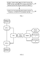
- FIG. 1 is a schematic flowchart of a data processing method according to an embodiment of the present invention
- FIG. 2 is a schematic structural diagram of a PCI-E bus system involved in an embodiment corresponding to FIG. 1 ;
- FIG. 3 is a schematic structural diagram of a data processing apparatus according to another embodiment of the present invention.
- FIG. 4 is a schematic structural diagram of a data processing apparatus according to another embodiment of the present invention.
- FIG. 5 is a schematic structural diagram of a PCI-E bus system according to another embodiment of the present invention.
- FIG. 6 is a schematic structural diagram of a server according to another embodiment of the present invention.
- FIG. 1 is a schematic flowchart of a data processing method according to an embodiment of the present invention. As shown in FIG. 1 , the data processing method in this embodiment may include:
- Configure address information of a PCI-E memory of a PCI-E device so that the PCI-E device stores data received by the PCI-E device in the PCI-E memory.
- An executor of 101 and 102 may be an operating system.
- the operating system may also determine the CPU that is used for accessing the data by pre-specifying the CPU (for example, a main CPU) that is used for accessing the data stored in the PCI-E memory. For a specific determining method, reference may be made to relevant contents in the prior art, which is not repeated here.
- the determined CPU may be specifically controlled to access, according to the address information of the PCI-E memory, the data stored in the PCI-E memory.
- the data stored in the PCI-E memory may be specifically copied into a memory of the determined CPU, and the determined CPU may be controlled to access the data stored in the memory of the determined CPU.
- the PCI-E memory may be located on a PCI-E bus, that is, the PCI-E memory may be set in front of a switch (Switch).
- the PCI-E memory may also be connected to the PCI-E bus, that is, the PCI-E memory may be similar to a PCI-E device and behind the switch (Switch), and may be connected to the CPU through a bus.
- the address information of the PCI-E memory of the PCI-E device is configured, so that after the PCI-E device stores the data received by the PCI-E device in the PCI-E memory, the CPU can be controlled to access the data stored in the PCI-E memory.
- the PCI-E device stores the data received by the PCI-E device in a memory of the CPU, when the data stored in the memory of the CPU is accessed by another CPU, a part of a bandwidth of a bus between the another CPU and the CPU is occupied and a bus through which the CPU accesses the memory that corresponds the CPU is occupied, thereby improving a utilization rate of the CPU.
- a PCI-E bus system as shown in FIG. 2 is taken as an example in the following.
- a CPU 1 is connected to a CPU 2 through a quick path interconnect (Quick Path Interconnect, referred to as QPI) bus; the CPU 1 and the CPU 2 are connected to an input output hub (Input Output Hub, referred to as IOH) through the QPI bus; the IOH is connected to a switch (Switch) through a root complex (Root Complex); and the switch (Switch) is connected to a PCI-E device 1, a PCI-E device 2, and a PCI-E memory.
- QPI quick path interconnect
- IOH input output hub
- IOH input output hub
- the switch is connected to a switch (Switch) through a root complex (Root Complex)
- the switch (Switch) is connected to a PCI-E device 1, a PCI-E device 2, and a PCI-E memory.
- an operating system running on the CPU 1 and an operating system running on the CPU 2 configure address information of a PCI-E memory of the PCI-E device 1 and address information of a PCI-E memory of the PCI-E device 2, so that the PCI-E device 1 or the PCI-E device 2 stores data received by the PCI-E device 2 in the PCI-E memory.
- the operating system controls the CPU 1 to access the data stored in the PCI-E memory, so that the CPU 1 processes the data.
- the CPU 1 may further transfer information through the QPI bus between the CPU 1 and the CPU 2 at the same time when the CPU 1 accesses the data stored in the PCI-E memory.
- the CPU 1 does not occupy a bandwidth of the QPI bus between the CPU 1 and the CPU 2 when accessing the data stored in the PCI-E memory.
- the CPU 2 may also access other data stored in its corresponding memory at the same time when the CPU 1 accesses the data stored in the PCI-E memory, thereby improving utilization rates of the CPU 1 and the CPU 2.
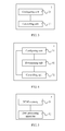
- FIG. 3 is a schematic structural diagram of a data processing apparatus according to another embodiment of the present invention.
- a data processing apparatus 3 in this embodiment may include a configuring unit 31 and a controlling unit 32.
- the configuring unit 31 is configured to configure address information of a PCI-E memory of a PCI-E device, so that the PCI-E device stores data received by the PCI-E device in the PCI-E memory; and the controlling unit 32 is configured to control a CPU to access the data stored in the PCI-E memory, so that the CPU processes the data.
- the method in the foregoing embodiment corresponding to FIG. 1 may be implemented by the data processing apparatus provided in this embodiment.
- a data processing apparatus 4 in this embodiment may further include a determining unit 41, configured to determine the CPU that is used for accessing the data by pre-specifying the CPU that is used for accessing the data stored in the PCI-E memory, so that the controlling unit 32 controls the CPU determined by the determining unit 41 to access the data stored in the PCI-E memory.
- a determining unit 41 configured to determine the CPU that is used for accessing the data by pre-specifying the CPU that is used for accessing the data stored in the PCI-E memory, so that the controlling unit 32 controls the CPU determined by the determining unit 41 to access the data stored in the PCI-E memory.
- controlling unit 32 in this embodiment may specifically control the CPU to access, according to the address information of the PCI-E memory, the data stored in the PCI-E memory.
- controlling unit 32 in this embodiment may also specifically copy the data stored in the PCI-E memory into a memory of the CPU, and control the CPU to access the data stored in the memory of the CPU.
- the PCI-E memory may be located on a PCI-E bus, that is, the PCI-E memory may be set in front of a switch (Switch).
- the PCI-E memory may also be connected to the PCI-E bus, that is, the PCI-E memory may be similar to a PCI-E device and behind the switch (Switch), and may be connected to the CPU through a bus.
- the address information of the PCI-E memory of the PCI-E device is configured by the configuring unit, so that after the PCI-E device stores the data received by the PCI-E device in the PCI-E memory, the controlling unit can control the CPU to access the data stored in the PCI-E memory.
- the PCI-E device stores the data received by the PCI-E device in a memory of the CPU, when the data stored in the memory of the CPU is accessed by another CPU, a part of a bandwidth of a bus between the another CPU and the CPU is occupied and a bus through which the CPU accesses the memory that corresponds the CPU is occupied, thereby improving a utilization rate of the CPU.
- FIG. 5 is a schematic structural diagram of a PCI-E bus system 5 according to another embodiment of the present invention.
- the PCI-E bus system in this embodiment may include a PCI-E memory 51, and a data processing apparatus 52 provided in the embodiment corresponding to FIG. 3 or FIG. 4 , where the PCI-E memory 51 is configured to store data received by the PCI-E device.
- FIG. 6 is a schematic structural diagram of a server 6 according to another embodiment of the present invention.
- the server in this embodiment may include a CPU 61, and a PCI-E bus system 62 provided in the embodiment corresponding to FIG. 5 , where the CPU 61 is configured to access the data stored in the PCI-E memory, and process the data.
- the disclosed system, apparatus, and method may be implemented in other ways.
- the apparatus embodiments described in the following are only exemplary, for example, the unit division is only logic function division, and there may be other division ways during practical implementation, for example, multiple units or components may be combined or integrated into another system, or some features may be omitted or may not be executed.
- the shown or discussed mutual couplings or direct couplings or communication connections may be implemented through some interfaces. Indirect couplings or communication connections between apparatuses or units may be electrical, mechanical, or in other forms.
- the units described as separated parts may or may not be physically separated from each other, and the parts shown as units may or may not be physical units, that is, they may be located at the same place, and may also be distributed to multiple network elements. A part or all of the units may be selected according to an actual requirement to achieve the objectives of the solutions in the embodiments.
- function units in the embodiments of the present invention may be integrated into a processing unit, each of the units may also exist separately and physically, and two or more units may also be integrated into one unit.
- the integrated unit may be implemented in the form of hardware, and may also be implemented in the form of a software function unit.
- the integrated unit is implemented in the form of a software function unit and is sold or used as an independent product, it may be stored in a computer readable storage medium.
- the computer software product is stored in a storage medium and includes several instructions for instructing a computer device (which may be a personal computer, a server, or a network device, and so on.) to execute all or a part of steps of the methods described in the embodiments of the present invention.
- the storage medium includes: any medium that is capable of storing grogram codes, such as a USB-disk, a removable hard disk, a read-only memory (Read-Only Memory, referred to as ROM), a random access memory (Random Access Memory, referred to as RAM), a magnetic disk, or an optical disk.
- grogram codes such as a USB-disk, a removable hard disk, a read-only memory (Read-Only Memory, referred to as ROM), a random access memory (Random Access Memory, referred to as RAM), a magnetic disk, or an optical disk.
Landscapes
- Engineering & Computer Science (AREA)
- Theoretical Computer Science (AREA)
- Physics & Mathematics (AREA)
- General Engineering & Computer Science (AREA)
- General Physics & Mathematics (AREA)
- Human Computer Interaction (AREA)
- Bus Control (AREA)
Abstract
Description
- Embodiments of the present invention relate to communications technologies, and particularly, to a data processing method and apparatus, an expansion peripheral component interconnect express (Peripheral Component Interconnect Express, referred to as PCI-E) bus system, and a server.
- Generally, a server may include a plurality of central processing units (Central Process Unit, referred to as CPU), and each of the CPUs is interconnected in the form of a bus, where a CPU may be connected to a device, that is, a PCI-E device, through a PCI-E bus system. The PCI-E device stores data received by the PCI-E device in a memory of the CPU according to obtained address information of the memory of the CPU.
- However, when another CPU needs to access the data, it needs to access the data stored in the memory, through a bus between the another CPU and the CPU that corresponds to the memory that stores the received data, and a bus between the CPU and the memory that corresponds to the CPU. Therefore, a part of a bandwidth of the bus between the another CPU and the CPU is occupied, and a bus through which the CPU accesses the memory that corresponds the CPU is occupied, thereby reducing a utilization rate of the CPU.
- Embodiments of the present invention provide a data processing method and apparatus, a PCI-E bus system, and a server, so as to improve a utilization rate of a CPU.
- In one aspect, an embodiment of the present invention provides a data processing method, including:
- configuring address information of a PCI-E memory of a PCI-E device, so that the PCI-E device stores data received by the PCI-E device in the PCI-E memory; and
- controlling a CPU to access the data stored in the PCI-E memory, so that the CPU processes the data.
- In another aspect, an embodiment of the present invention provides a data processing apparatus, including:
- a configuring unit, configured to configure address information of a PCI-E memory of a PCI-E device, so that the PCI-E device stores data received by the PCI-E device in the PCI-E memory; and
- a controlling unit, configured to control a CPU to access the data stored in the PCI-E memory, so that the CPU processes the data.
- In another aspect, an embodiment of the present invention provides a PCI-E bus system, including a PCI-E memory and the foregoing data processing apparatus, where the PCI-E memory is configured to store data received by the PCI-E device.
- In another aspect, an embodiment of the present invention provides a server, including a CPU and the foregoing PCI-E bus system, where the CPU is configured to access the data stored in the PCI-E memory, and process the data.
- It can be seen from the foregoing technical solutions, in the embodiments of the present invention, the address information of the PCI-E memory of the PCI-E device is configured, so that after the PCI-E device stores the data received by the PCI-E device in the PCI-E memory, the CPU can be controlled to access the data stored in the PCI-E memory. This can avoid a problem that in the prior art, because the PCI-E device stores the data received by the PCI-E in a memory of the CPU, when the data stored in the memory of the CPU is accessed by another CPU, a part of a bandwidth of a bus between the another CPU and the CPU is occupied and a bus through which the CPU accesses the memory that corresponds the CPU is occupied, thereby improving a utilization rate of the CPU.
- To describe the technical solutions in the embodiments of the present invention or in the prior art more clearly, the accompanying drawings required for describing the embodiments or the prior art are briefly introduced in the following. Evidently, the accompanying drawings in the following description are some embodiments of the present invention, and persons of ordinary skill in the art may also obtain other drawings according to these accompanying drawings without creative efforts.
-
FIG. 1 is a schematic flowchart of a data processing method according to an embodiment of the present invention; -
FIG. 2 is a schematic structural diagram of a PCI-E bus system involved in an embodiment corresponding toFIG. 1 ; -
FIG. 3 is a schematic structural diagram of a data processing apparatus according to another embodiment of the present invention; -
FIG. 4 is a schematic structural diagram of a data processing apparatus according to another embodiment of the present invention; -
FIG. 5 is a schematic structural diagram of a PCI-E bus system according to another embodiment of the present invention; and -
FIG. 6 is a schematic structural diagram of a server according to another embodiment of the present invention. - In order to make the objectives, technical solutions, and advantages of the embodiments of the present invention clearer, the technical solutions in the embodiments of the present invention are described clearly and completely in the following with reference to the accompanying drawings in the embodiments of the present invention. Evidently, the embodiments to be described are only a part rather than all of the embodiments of the present invention. Based on the embodiments of the present invention, other embodiments that are obtained by persons of ordinary skill in the art without creative efforts all fall within the protection scope of the present invention.
-
FIG. 1 is a schematic flowchart of a data processing method according to an embodiment of the present invention. As shown inFIG. 1 , the data processing method in this embodiment may include: - 101: Configure address information of a PCI-E memory of a PCI-E device, so that the PCI-E device stores data received by the PCI-E device in the PCI-E memory.
- 102: Control a CPU to access the data stored in the PCI-E memory, so that the CPU processes the data.
- An executor of 101 and 102 may be an operating system.
- Further, before 102, the operating system may also determine the CPU that is used for accessing the data by pre-specifying the CPU (for example, a main CPU) that is used for accessing the data stored in the PCI-E memory. For a specific determining method, reference may be made to relevant contents in the prior art, which is not repeated here.
- Optionally, in 102, the determined CPU may be specifically controlled to access, according to the address information of the PCI-E memory, the data stored in the PCI-E memory.
- Optionally, in 102, the data stored in the PCI-E memory may be specifically copied into a memory of the determined CPU, and the determined CPU may be controlled to access the data stored in the memory of the determined CPU.
- Optionally, the PCI-E memory may be located on a PCI-E bus, that is, the PCI-E memory may be set in front of a switch (Switch). Optionally, the PCI-E memory may also be connected to the PCI-E bus, that is, the PCI-E memory may be similar to a PCI-E device and behind the switch (Switch), and may be connected to the CPU through a bus.
- In this embodiment, the address information of the PCI-E memory of the PCI-E device is configured, so that after the PCI-E device stores the data received by the PCI-E device in the PCI-E memory, the CPU can be controlled to access the data stored in the PCI-E memory. This can avoid a problem that in the prior art, because the PCI-E device stores the data received by the PCI-E device in a memory of the CPU, when the data stored in the memory of the CPU is accessed by another CPU, a part of a bandwidth of a bus between the another CPU and the CPU is occupied and a bus through which the CPU accesses the memory that corresponds the CPU is occupied, thereby improving a utilization rate of the CPU.
- To make the method provided in this embodiment of the present invention clearer, a PCI-E bus system as shown in
FIG. 2 is taken as an example in the following. In the PCI-E bus system as shown inFIG. 2 , aCPU 1 is connected to aCPU 2 through a quick path interconnect (Quick Path Interconnect, referred to as QPI) bus; theCPU 1 and theCPU 2 are connected to an input output hub (Input Output Hub, referred to as IOH) through the QPI bus; the IOH is connected to a switch (Switch) through a root complex (Root Complex); and the switch (Switch) is connected to a PCI-E device 1, a PCI-E device 2, and a PCI-E memory. First, an operating system running on theCPU 1 and an operating system running on theCPU 2 configure address information of a PCI-E memory of the PCI-E device 1 and address information of a PCI-E memory of the PCI-E device 2, so that the PCI-E device 1 or the PCI-E device 2 stores data received by the PCI-E device 2 in the PCI-E memory. Then, the operating system controls theCPU 1 to access the data stored in the PCI-E memory, so that theCPU 1 processes the data. TheCPU 1 may further transfer information through the QPI bus between theCPU 1 and theCPU 2 at the same time when theCPU 1 accesses the data stored in the PCI-E memory. TheCPU 1 does not occupy a bandwidth of the QPI bus between theCPU 1 and theCPU 2 when accessing the data stored in the PCI-E memory. In addition, theCPU 2 may also access other data stored in its corresponding memory at the same time when theCPU 1 accesses the data stored in the PCI-E memory, thereby improving utilization rates of theCPU 1 and theCPU 2. - It should be noted that, for simple description, the foregoing method embodiments are expressed as a series of actions. But those skilled in the art should know that the present invention is not limited to an order of described actions, because according to the present invention, some steps may be performed in another order or be performed simultaneously. Next, those skilled in the art should also know that all the embodiments described in the specification are exemplary embodiments, and that involved actions and modules are not necessarily required in the present invention.
- In the foregoing embodiments, the description of each embodiment has its emphasis, and for a part that is not detailed in a certain embodiment, reference may be made to the relevant description of another embodiment.
-
FIG. 3 is a schematic structural diagram of a data processing apparatus according to another embodiment of the present invention. As shown inFIG. 3 , adata processing apparatus 3 in this embodiment may include a configuringunit 31 and a controllingunit 32. The configuringunit 31 is configured to configure address information of a PCI-E memory of a PCI-E device, so that the PCI-E device stores data received by the PCI-E device in the PCI-E memory; and the controllingunit 32 is configured to control a CPU to access the data stored in the PCI-E memory, so that the CPU processes the data. - The method in the foregoing embodiment corresponding to
FIG. 1 may be implemented by the data processing apparatus provided in this embodiment. - Further, as shown in
FIG. 4 , adata processing apparatus 4 in this embodiment may further include a determiningunit 41, configured to determine the CPU that is used for accessing the data by pre-specifying the CPU that is used for accessing the data stored in the PCI-E memory, so that the controllingunit 32 controls the CPU determined by the determiningunit 41 to access the data stored in the PCI-E memory. - Optionally, the controlling
unit 32 in this embodiment may specifically control the CPU to access, according to the address information of the PCI-E memory, the data stored in the PCI-E memory. - Optionally, the controlling
unit 32 in this embodiment may also specifically copy the data stored in the PCI-E memory into a memory of the CPU, and control the CPU to access the data stored in the memory of the CPU. - Optionally, the PCI-E memory may be located on a PCI-E bus, that is, the PCI-E memory may be set in front of a switch (Switch). Optionally, the PCI-E memory may also be connected to the PCI-E bus, that is, the PCI-E memory may be similar to a PCI-E device and behind the switch (Switch), and may be connected to the CPU through a bus.
- In this embodiment, the address information of the PCI-E memory of the PCI-E device is configured by the configuring unit, so that after the PCI-E device stores the data received by the PCI-E device in the PCI-E memory, the controlling unit can control the CPU to access the data stored in the PCI-E memory. This can avoid a problem that in the prior art, because the PCI-E device stores the data received by the PCI-E device in a memory of the CPU, when the data stored in the memory of the CPU is accessed by another CPU, a part of a bandwidth of a bus between the another CPU and the CPU is occupied and a bus through which the CPU accesses the memory that corresponds the CPU is occupied, thereby improving a utilization rate of the CPU.
-
FIG. 5 is a schematic structural diagram of a PCI-E bus system 5 according to another embodiment of the present invention. As shown inFIG. 5 , the PCI-E bus system in this embodiment may include a PCI-E memory 51, and adata processing apparatus 52 provided in the embodiment corresponding toFIG. 3 or FIG. 4 , where the PCI-E memory 51 is configured to store data received by the PCI-E device. -
FIG. 6 is a schematic structural diagram of aserver 6 according to another embodiment of the present invention. As shown inFIG. 6 , the server in this embodiment may include aCPU 61, and a PCI-E bus system 62 provided in the embodiment corresponding toFIG. 5 , where theCPU 61 is configured to access the data stored in the PCI-E memory, and process the data. - Those skilled in the art may clearly understand that, to describe conveniently and simply, for specific working processes of the system, the apparatus, and the unit described in the foregoing, reference may be made to corresponding processes in the foregoing method embodiments, which are not repeated here.
- In several embodiments of the present invention, it should be understood that the disclosed system, apparatus, and method may be implemented in other ways. For example, the apparatus embodiments described in the following are only exemplary, for example, the unit division is only logic function division, and there may be other division ways during practical implementation, for example, multiple units or components may be combined or integrated into another system, or some features may be omitted or may not be executed. In addition, the shown or discussed mutual couplings or direct couplings or communication connections may be implemented through some interfaces. Indirect couplings or communication connections between apparatuses or units may be electrical, mechanical, or in other forms.
- The units described as separated parts may or may not be physically separated from each other, and the parts shown as units may or may not be physical units, that is, they may be located at the same place, and may also be distributed to multiple network elements. A part or all of the units may be selected according to an actual requirement to achieve the objectives of the solutions in the embodiments.
- In addition, function units in the embodiments of the present invention may be integrated into a processing unit, each of the units may also exist separately and physically, and two or more units may also be integrated into one unit. The integrated unit may be implemented in the form of hardware, and may also be implemented in the form of a software function unit.
- If the integrated unit is implemented in the form of a software function unit and is sold or used as an independent product, it may be stored in a computer readable storage medium. Based on such understanding, the technical solutions of the present invention essentially, or the part contributing to the prior art, or all or a part of the technical solutions may be implemented in the form of a software product. The computer software product is stored in a storage medium and includes several instructions for instructing a computer device (which may be a personal computer, a server, or a network device, and so on.) to execute all or a part of steps of the methods described in the embodiments of the present invention. The storage medium includes: any medium that is capable of storing grogram codes, such as a USB-disk, a removable hard disk, a read-only memory (Read-Only Memory, referred to as ROM), a random access memory (Random Access Memory, referred to as RAM), a magnetic disk, or an optical disk.
Claims (10)
- A data processing method, comprising:configuring address information of a PCI-E memory of a PCI-E device, so that the PCI-E device stores data received by the PCI-E device in the PCI-E memory; andcontrolling a CPU to access the data stored in the PCI-E memory, so that the CPU processes the data.
- The method according to claim 1, wherein:before the controlling the CPU to access the data stored in the PCI-E memory, so that the CPU processes the data, further comprising:determining the CPU that is used for accessing the data by pre-specifying the CPU that is used for accessing the data stored in the PCI-E memory.
- The method according to claim 1 or 2, wherein the controlling the CPU to access the data stored in the PCI-E memory comprises:controlling the CPU to access, according to the address information of the PCI-E memory, the data stored in the PCI-E memory; orcopying the data stored in the PCI-E memory into a memory of the CPU, and controlling the CPU to access the data stored in the memory of the CPU.
- The method according to any one of claims 1 to 3, wherein the PCI-E memory is located on a PCI-E bus or connected to the PCI-E bus.
- A data processing apparatus, comprising:a configuring unit, configured to configure address information of a PCI-E memory of a PCI-E device, so that the PCI-E device stores data received by the PCI-E device in the PCI-E memory; anda controlling unit, configured to control a CPU to access the data stored in the PCI-E memory, so that the CPU processes the data.
- The apparatus according to claim 5, further comprising a determining unit, configured to:determine the CPU that is used for accessing the data by pre-specifying the CPU that is used for accessing the data stored in the PCI-E memory, so that the controlling unit controls the determined CPU to access the data stored in the PCI-E memory.
- The apparatus according to claim 5 or 6, wherein the controlling unit is specifically configured to:control the CPU to access, according to the address information of the PCI-E memory, the data stored in the PCI-E memory; orcopy the data stored in the PCI-E memory into a memory of the CPU, and control the CPU to access the data stored in the memory of the CPU.
- The apparatus according to any one of claims 5 to 7, wherein the PCI-E memory is located on a PCI-E bus or connected to the PCI-E bus.
- A PCI-E bus system, comprising a PCI-E memory and the data processing apparatus according to any one of claims 5 to 8, wherein the PCI-E memory is configured to store data received by the PCI-E device.
- A server, comprising a CPU and the PCI-E bus system according to claim 9, wherein the CPU is configured to access the data stored in the PCI-E memory, and process the data.
Applications Claiming Priority (2)
| Application Number | Priority Date | Filing Date | Title |
|---|---|---|---|
| CN201110185059.9A CN102393838B (en) | 2011-07-04 | 2011-07-04 | Data processing method and device, PCI-E (peripheral component interface-express) bus system, and server |
| PCT/CN2011/083754 WO2012103768A1 (en) | 2011-07-04 | 2011-12-09 | Method and apparatus for data processing, pci-e bus system and server |
Publications (3)
| Publication Number | Publication Date |
|---|---|
| EP2620876A1 true EP2620876A1 (en) | 2013-07-31 |
| EP2620876A4 EP2620876A4 (en) | 2014-11-05 |
| EP2620876B1 EP2620876B1 (en) | 2018-01-24 |
Family
ID=45861166
Family Applications (1)
| Application Number | Title | Priority Date | Filing Date |
|---|---|---|---|
| EP11857907.7A Active EP2620876B1 (en) | 2011-07-04 | 2011-12-09 | Method and apparatus for data processing, pci-e bus system and server |
Country Status (4)
| Country | Link |
|---|---|
| US (1) | US20130238871A1 (en) |
| EP (1) | EP2620876B1 (en) |
| CN (1) | CN102393838B (en) |
| WO (1) | WO2012103768A1 (en) |
Families Citing this family (5)
| Publication number | Priority date | Publication date | Assignee | Title |
|---|---|---|---|---|
| CN104484021A (en) * | 2014-12-23 | 2015-04-01 | 浪潮电子信息产业股份有限公司 | Server system with expandable memory |
| CN105183684B (en) * | 2015-09-09 | 2019-01-25 | 成都思鸿维科技有限责任公司 | Data processing equipment, method and system |
| CN106713183B (en) | 2015-10-30 | 2020-03-17 | 新华三技术有限公司 | Interface board of network equipment, network equipment and message forwarding method |
| CN109154791B (en) * | 2017-02-24 | 2021-08-20 | 京瓷办公信息系统株式会社 | Reciprocating mechanism of moving body, cleaning mechanism, optical scanning device, and image forming apparatus |
| WO2019159716A1 (en) * | 2018-02-14 | 2019-08-22 | 日立オートモティブシステムズ株式会社 | Electronic control device |
Citations (3)
| Publication number | Priority date | Publication date | Assignee | Title |
|---|---|---|---|---|
| WO2006113134A2 (en) * | 2005-04-18 | 2006-10-26 | Cisco Technology, Inc. | Pci express switch with encryption and queues for performance enhancement |
| US20070280278A1 (en) * | 2006-05-30 | 2007-12-06 | Masatoshi Ezawa | Switching device |
| WO2010050092A1 (en) * | 2008-10-29 | 2010-05-06 | 日本電気株式会社 | Information processing system |
Family Cites Families (10)
| Publication number | Priority date | Publication date | Assignee | Title |
|---|---|---|---|---|
| US7421532B2 (en) * | 2003-11-18 | 2008-09-02 | Topside Research, Llc | Switching with transparent and non-transparent ports |
| US7398427B2 (en) * | 2004-07-08 | 2008-07-08 | International Business Machines Corporation | Isolation of input/output adapter error domains |
| US8103993B2 (en) * | 2006-05-24 | 2012-01-24 | International Business Machines Corporation | Structure for dynamically allocating lanes to a plurality of PCI express connectors |
| CN101178697B (en) * | 2007-12-12 | 2011-08-03 | 杭州华三通信技术有限公司 | PCIE apparatus satellite communication method and system |
| US8850159B2 (en) * | 2008-04-29 | 2014-09-30 | Broadcom Corporation | Method and system for latency optimized ATS usage |
| CN101281453B (en) * | 2008-05-13 | 2010-10-27 | 华为技术有限公司 | Memory apparatus cascading method, memory system as well as memory apparatus |
| CN101639930B (en) * | 2008-08-01 | 2012-07-04 | 辉达公司 | Method and system for processing graphical data by a series of graphical processors |
| US8225019B2 (en) * | 2008-09-22 | 2012-07-17 | Micron Technology, Inc. | SATA mass storage device emulation on a PCIe interface |
| JP5281942B2 (en) * | 2009-03-26 | 2013-09-04 | 株式会社日立製作所 | Computer and its fault handling method |
| CN101799795B (en) * | 2009-12-30 | 2011-11-02 | 龙芯中科技术有限公司 | 1553B bus monitor and bus system with same |
-
2011
- 2011-07-04 CN CN201110185059.9A patent/CN102393838B/en active Active
- 2011-12-09 EP EP11857907.7A patent/EP2620876B1/en active Active
- 2011-12-09 WO PCT/CN2011/083754 patent/WO2012103768A1/en unknown
-
2013
- 2013-04-26 US US13/871,596 patent/US20130238871A1/en not_active Abandoned
Patent Citations (3)
| Publication number | Priority date | Publication date | Assignee | Title |
|---|---|---|---|---|
| WO2006113134A2 (en) * | 2005-04-18 | 2006-10-26 | Cisco Technology, Inc. | Pci express switch with encryption and queues for performance enhancement |
| US20070280278A1 (en) * | 2006-05-30 | 2007-12-06 | Masatoshi Ezawa | Switching device |
| WO2010050092A1 (en) * | 2008-10-29 | 2010-05-06 | 日本電気株式会社 | Information processing system |
Non-Patent Citations (1)
| Title |
|---|
| See also references of WO2012103768A1 * |
Also Published As
| Publication number | Publication date |
|---|---|
| US20130238871A1 (en) | 2013-09-12 |
| WO2012103768A1 (en) | 2012-08-09 |
| CN102393838A (en) | 2012-03-28 |
| EP2620876B1 (en) | 2018-01-24 |
| EP2620876A4 (en) | 2014-11-05 |
| CN102393838B (en) | 2015-03-11 |
Similar Documents
| Publication | Publication Date | Title |
|---|---|---|
| EP3612942B1 (en) | Queue management for direct memory access | |
| US9864606B2 (en) | Methods for configurable hardware logic device reloading and devices thereof | |
| US10411953B2 (en) | Virtual machine fault tolerance method, apparatus, and system | |
| WO2016037503A1 (en) | Configuration method and device of pcie topology | |
| US20120254881A1 (en) | Parallel computer system and program | |
| US10303474B2 (en) | Data read/write method and apparatus, storage device, and computer system | |
| WO2017000822A1 (en) | Transmission control method and device for direct memory access | |
| CN110659151B (en) | Data verification method and device and storage medium | |
| EP3223162B1 (en) | Configurable on-chip interconnection system and method and apparatus for implementing same, and storage medium | |
| EP2620876A1 (en) | Method and apparatus for data processing, pci-e bus system and server | |
| US10534563B2 (en) | Method and system for handling an asynchronous event request command in a solid-state drive | |
| CN106648832B (en) | Device and method for improving resource utilization rate of virtual machine | |
| US20220004873A1 (en) | Techniques to manage training or trained models for deep learning applications | |
| EP2808778A1 (en) | Capacity expansion method and device | |
| WO2018076882A1 (en) | Operating method for storage device, and physical server | |
| US9692813B2 (en) | Dynamic assignment of transfers of blocks of data | |
| US10025608B2 (en) | Quiesce handling in multithreaded environments | |
| EP2778935B1 (en) | Efficient Input/Output (I/O) operations | |
| US9519527B1 (en) | System and method for performing internal system interface-based communications in management controller | |
| US10616317B2 (en) | Method and system for affinity load balancing | |
| US10467156B1 (en) | System and method of improving efficiency in parallel data processing of a RAID array | |
| US8891515B2 (en) | Method for node communication | |
| US20150213124A1 (en) | Continuously blocking query result data for a remote query | |
| US10579394B2 (en) | Control method and control device | |
| US20190179778A1 (en) | System memory controller with client preemption |
Legal Events
| Date | Code | Title | Description |
|---|---|---|---|
| PUAI | Public reference made under article 153(3) epc to a published international application that has entered the european phase |
Free format text: ORIGINAL CODE: 0009012 |
|
| 17P | Request for examination filed |
Effective date: 20130426 |
|
| AK | Designated contracting states |
Kind code of ref document: A1 Designated state(s): AL AT BE BG CH CY CZ DE DK EE ES FI FR GB GR HR HU IE IS IT LI LT LU LV MC MK MT NL NO PL PT RO RS SE SI SK SM TR |
|
| DAX | Request for extension of the european patent (deleted) | ||
| A4 | Supplementary search report drawn up and despatched |
Effective date: 20141008 |
|
| RIC1 | Information provided on ipc code assigned before grant |
Ipc: G06F 3/06 20060101ALI20141001BHEP Ipc: G06F 13/16 20060101AFI20141001BHEP |
|
| 17Q | First examination report despatched |
Effective date: 20160613 |
|
| GRAP | Despatch of communication of intention to grant a patent |
Free format text: ORIGINAL CODE: EPIDOSNIGR1 |
|
| INTG | Intention to grant announced |
Effective date: 20161216 |
|
| GRAS | Grant fee paid |
Free format text: ORIGINAL CODE: EPIDOSNIGR3 |
|
| GRAJ | Information related to disapproval of communication of intention to grant by the applicant or resumption of examination proceedings by the epo deleted |
Free format text: ORIGINAL CODE: EPIDOSDIGR1 |
|
| GRAL | Information related to payment of fee for publishing/printing deleted |
Free format text: ORIGINAL CODE: EPIDOSDIGR3 |
|
| INTC | Intention to grant announced (deleted) | ||
| GRAP | Despatch of communication of intention to grant a patent |
Free format text: ORIGINAL CODE: EPIDOSNIGR1 |
|
| INTG | Intention to grant announced |
Effective date: 20170712 |
|
| GRAA | (expected) grant |
Free format text: ORIGINAL CODE: 0009210 |
|
| AK | Designated contracting states |
Kind code of ref document: B1 Designated state(s): AL AT BE BG CH CY CZ DE DK EE ES FI FR GB GR HR HU IE IS IT LI LT LU LV MC MK MT NL NO PL PT RO RS SE SI SK SM TR |
|
| REG | Reference to a national code |
Ref country code: GB Ref legal event code: FG4D |
|
| REG | Reference to a national code |
Ref country code: CH Ref legal event code: EP |
|
| REG | Reference to a national code |
Ref country code: AT Ref legal event code: REF Ref document number: 966148 Country of ref document: AT Kind code of ref document: T Effective date: 20180215 |
|
| REG | Reference to a national code |
Ref country code: IE Ref legal event code: FG4D |
|
| REG | Reference to a national code |
Ref country code: DE Ref legal event code: R096 Ref document number: 602011045406 Country of ref document: DE |
|
| REG | Reference to a national code |
Ref country code: NL Ref legal event code: FP |
|
| REG | Reference to a national code |
Ref country code: LT Ref legal event code: MG4D |
|
| REG | Reference to a national code |
Ref country code: AT Ref legal event code: MK05 Ref document number: 966148 Country of ref document: AT Kind code of ref document: T Effective date: 20180124 |
|
| PG25 | Lapsed in a contracting state [announced via postgrant information from national office to epo] |
Ref country code: ES Free format text: LAPSE BECAUSE OF FAILURE TO SUBMIT A TRANSLATION OF THE DESCRIPTION OR TO PAY THE FEE WITHIN THE PRESCRIBED TIME-LIMIT Effective date: 20180124 Ref country code: CY Free format text: LAPSE BECAUSE OF FAILURE TO SUBMIT A TRANSLATION OF THE DESCRIPTION OR TO PAY THE FEE WITHIN THE PRESCRIBED TIME-LIMIT Effective date: 20180124 Ref country code: LT Free format text: LAPSE BECAUSE OF FAILURE TO SUBMIT A TRANSLATION OF THE DESCRIPTION OR TO PAY THE FEE WITHIN THE PRESCRIBED TIME-LIMIT Effective date: 20180124 Ref country code: FI Free format text: LAPSE BECAUSE OF FAILURE TO SUBMIT A TRANSLATION OF THE DESCRIPTION OR TO PAY THE FEE WITHIN THE PRESCRIBED TIME-LIMIT Effective date: 20180124 Ref country code: NO Free format text: LAPSE BECAUSE OF FAILURE TO SUBMIT A TRANSLATION OF THE DESCRIPTION OR TO PAY THE FEE WITHIN THE PRESCRIBED TIME-LIMIT Effective date: 20180424 Ref country code: HR Free format text: LAPSE BECAUSE OF FAILURE TO SUBMIT A TRANSLATION OF THE DESCRIPTION OR TO PAY THE FEE WITHIN THE PRESCRIBED TIME-LIMIT Effective date: 20180124 |
|
| PG25 | Lapsed in a contracting state [announced via postgrant information from national office to epo] |
Ref country code: AT Free format text: LAPSE BECAUSE OF FAILURE TO SUBMIT A TRANSLATION OF THE DESCRIPTION OR TO PAY THE FEE WITHIN THE PRESCRIBED TIME-LIMIT Effective date: 20180124 Ref country code: GR Free format text: LAPSE BECAUSE OF FAILURE TO SUBMIT A TRANSLATION OF THE DESCRIPTION OR TO PAY THE FEE WITHIN THE PRESCRIBED TIME-LIMIT Effective date: 20180425 Ref country code: PL Free format text: LAPSE BECAUSE OF FAILURE TO SUBMIT A TRANSLATION OF THE DESCRIPTION OR TO PAY THE FEE WITHIN THE PRESCRIBED TIME-LIMIT Effective date: 20180124 Ref country code: BG Free format text: LAPSE BECAUSE OF FAILURE TO SUBMIT A TRANSLATION OF THE DESCRIPTION OR TO PAY THE FEE WITHIN THE PRESCRIBED TIME-LIMIT Effective date: 20180424 Ref country code: SE Free format text: LAPSE BECAUSE OF FAILURE TO SUBMIT A TRANSLATION OF THE DESCRIPTION OR TO PAY THE FEE WITHIN THE PRESCRIBED TIME-LIMIT Effective date: 20180124 Ref country code: IS Free format text: LAPSE BECAUSE OF FAILURE TO SUBMIT A TRANSLATION OF THE DESCRIPTION OR TO PAY THE FEE WITHIN THE PRESCRIBED TIME-LIMIT Effective date: 20180524 Ref country code: LV Free format text: LAPSE BECAUSE OF FAILURE TO SUBMIT A TRANSLATION OF THE DESCRIPTION OR TO PAY THE FEE WITHIN THE PRESCRIBED TIME-LIMIT Effective date: 20180124 Ref country code: RS Free format text: LAPSE BECAUSE OF FAILURE TO SUBMIT A TRANSLATION OF THE DESCRIPTION OR TO PAY THE FEE WITHIN THE PRESCRIBED TIME-LIMIT Effective date: 20180124 |
|
| REG | Reference to a national code |
Ref country code: DE Ref legal event code: R097 Ref document number: 602011045406 Country of ref document: DE |
|
| PG25 | Lapsed in a contracting state [announced via postgrant information from national office to epo] |
Ref country code: RO Free format text: LAPSE BECAUSE OF FAILURE TO SUBMIT A TRANSLATION OF THE DESCRIPTION OR TO PAY THE FEE WITHIN THE PRESCRIBED TIME-LIMIT Effective date: 20180124 Ref country code: AL Free format text: LAPSE BECAUSE OF FAILURE TO SUBMIT A TRANSLATION OF THE DESCRIPTION OR TO PAY THE FEE WITHIN THE PRESCRIBED TIME-LIMIT Effective date: 20180124 Ref country code: EE Free format text: LAPSE BECAUSE OF FAILURE TO SUBMIT A TRANSLATION OF THE DESCRIPTION OR TO PAY THE FEE WITHIN THE PRESCRIBED TIME-LIMIT Effective date: 20180124 Ref country code: IT Free format text: LAPSE BECAUSE OF FAILURE TO SUBMIT A TRANSLATION OF THE DESCRIPTION OR TO PAY THE FEE WITHIN THE PRESCRIBED TIME-LIMIT Effective date: 20180124 |
|
| PG25 | Lapsed in a contracting state [announced via postgrant information from national office to epo] |
Ref country code: DK Free format text: LAPSE BECAUSE OF FAILURE TO SUBMIT A TRANSLATION OF THE DESCRIPTION OR TO PAY THE FEE WITHIN THE PRESCRIBED TIME-LIMIT Effective date: 20180124 Ref country code: SM Free format text: LAPSE BECAUSE OF FAILURE TO SUBMIT A TRANSLATION OF THE DESCRIPTION OR TO PAY THE FEE WITHIN THE PRESCRIBED TIME-LIMIT Effective date: 20180124 Ref country code: CZ Free format text: LAPSE BECAUSE OF FAILURE TO SUBMIT A TRANSLATION OF THE DESCRIPTION OR TO PAY THE FEE WITHIN THE PRESCRIBED TIME-LIMIT Effective date: 20180124 Ref country code: SK Free format text: LAPSE BECAUSE OF FAILURE TO SUBMIT A TRANSLATION OF THE DESCRIPTION OR TO PAY THE FEE WITHIN THE PRESCRIBED TIME-LIMIT Effective date: 20180124 |
|
| PLBE | No opposition filed within time limit |
Free format text: ORIGINAL CODE: 0009261 |
|
| STAA | Information on the status of an ep patent application or granted ep patent |
Free format text: STATUS: NO OPPOSITION FILED WITHIN TIME LIMIT |
|
| 26N | No opposition filed |
Effective date: 20181025 |
|
| PG25 | Lapsed in a contracting state [announced via postgrant information from national office to epo] |
Ref country code: SI Free format text: LAPSE BECAUSE OF FAILURE TO SUBMIT A TRANSLATION OF THE DESCRIPTION OR TO PAY THE FEE WITHIN THE PRESCRIBED TIME-LIMIT Effective date: 20180124 |
|
| REG | Reference to a national code |
Ref country code: CH Ref legal event code: PL |
|
| PG25 | Lapsed in a contracting state [announced via postgrant information from national office to epo] |
Ref country code: MC Free format text: LAPSE BECAUSE OF FAILURE TO SUBMIT A TRANSLATION OF THE DESCRIPTION OR TO PAY THE FEE WITHIN THE PRESCRIBED TIME-LIMIT Effective date: 20180124 Ref country code: LU Free format text: LAPSE BECAUSE OF NON-PAYMENT OF DUE FEES Effective date: 20181209 |
|
| REG | Reference to a national code |
Ref country code: IE Ref legal event code: MM4A |
|
| REG | Reference to a national code |
Ref country code: BE Ref legal event code: MM Effective date: 20181231 |
|
| PG25 | Lapsed in a contracting state [announced via postgrant information from national office to epo] |
Ref country code: IE Free format text: LAPSE BECAUSE OF NON-PAYMENT OF DUE FEES Effective date: 20181209 |
|
| PG25 | Lapsed in a contracting state [announced via postgrant information from national office to epo] |
Ref country code: BE Free format text: LAPSE BECAUSE OF NON-PAYMENT OF DUE FEES Effective date: 20181231 |
|
| PG25 | Lapsed in a contracting state [announced via postgrant information from national office to epo] |
Ref country code: LI Free format text: LAPSE BECAUSE OF NON-PAYMENT OF DUE FEES Effective date: 20181231 Ref country code: CH Free format text: LAPSE BECAUSE OF NON-PAYMENT OF DUE FEES Effective date: 20181231 |
|
| PG25 | Lapsed in a contracting state [announced via postgrant information from national office to epo] |
Ref country code: MT Free format text: LAPSE BECAUSE OF NON-PAYMENT OF DUE FEES Effective date: 20181209 |
|
| PG25 | Lapsed in a contracting state [announced via postgrant information from national office to epo] |
Ref country code: TR Free format text: LAPSE BECAUSE OF FAILURE TO SUBMIT A TRANSLATION OF THE DESCRIPTION OR TO PAY THE FEE WITHIN THE PRESCRIBED TIME-LIMIT Effective date: 20180124 |
|
| PG25 | Lapsed in a contracting state [announced via postgrant information from national office to epo] |
Ref country code: PT Free format text: LAPSE BECAUSE OF FAILURE TO SUBMIT A TRANSLATION OF THE DESCRIPTION OR TO PAY THE FEE WITHIN THE PRESCRIBED TIME-LIMIT Effective date: 20180124 |
|
| PG25 | Lapsed in a contracting state [announced via postgrant information from national office to epo] |
Ref country code: MK Free format text: LAPSE BECAUSE OF NON-PAYMENT OF DUE FEES Effective date: 20180124 Ref country code: HU Free format text: LAPSE BECAUSE OF FAILURE TO SUBMIT A TRANSLATION OF THE DESCRIPTION OR TO PAY THE FEE WITHIN THE PRESCRIBED TIME-LIMIT; INVALID AB INITIO Effective date: 20111209 |
|
| PGFP | Annual fee paid to national office [announced via postgrant information from national office to epo] |
Ref country code: NL Payment date: 20231116 Year of fee payment: 13 |
|
| PGFP | Annual fee paid to national office [announced via postgrant information from national office to epo] |
Ref country code: GB Payment date: 20231102 Year of fee payment: 13 |
|
| PGFP | Annual fee paid to national office [announced via postgrant information from national office to epo] |
Ref country code: FR Payment date: 20231108 Year of fee payment: 13 Ref country code: DE Payment date: 20231031 Year of fee payment: 13 |