EP2544235A1 - Method for producing and method for designing soi wafer - Google Patents
Method for producing and method for designing soi wafer Download PDFInfo
- Publication number
- EP2544235A1 EP2544235A1 EP11750302A EP11750302A EP2544235A1 EP 2544235 A1 EP2544235 A1 EP 2544235A1 EP 11750302 A EP11750302 A EP 11750302A EP 11750302 A EP11750302 A EP 11750302A EP 2544235 A1 EP2544235 A1 EP 2544235A1
- Authority
- EP
- European Patent Office
- Prior art keywords
- insulator layer
- buried insulator
- soi
- soi wafer
- thickness
- Prior art date
- Legal status (The legal status is an assumption and is not a legal conclusion. Google has not performed a legal analysis and makes no representation as to the accuracy of the status listed.)
- Granted
Links
- 238000000034 method Methods 0.000 title claims abstract description 57
- 238000004519 manufacturing process Methods 0.000 title claims abstract description 37
- 239000012212 insulator Substances 0.000 claims abstract description 127
- 238000000206 photolithography Methods 0.000 claims abstract description 50
- XUIMIQQOPSSXEZ-UHFFFAOYSA-N Silicon Chemical compound [Si] XUIMIQQOPSSXEZ-UHFFFAOYSA-N 0.000 claims description 26
- 239000010703 silicon Substances 0.000 claims description 26
- 229910052710 silicon Inorganic materials 0.000 claims description 26
- VYPSYNLAJGMNEJ-UHFFFAOYSA-N Silicium dioxide Chemical compound O=[Si]=O VYPSYNLAJGMNEJ-UHFFFAOYSA-N 0.000 claims description 14
- 229910052814 silicon oxide Inorganic materials 0.000 claims description 14
- 229910052581 Si3N4 Inorganic materials 0.000 claims description 11
- HQVNEWCFYHHQES-UHFFFAOYSA-N silicon nitride Chemical compound N12[Si]34N5[Si]62N3[Si]51N64 HQVNEWCFYHHQES-UHFFFAOYSA-N 0.000 claims description 11
- 235000012431 wafers Nutrition 0.000 description 129
- 239000010408 film Substances 0.000 description 49
- 238000004088 simulation Methods 0.000 description 17
- 230000005764 inhibitory process Effects 0.000 description 16
- 230000000052 comparative effect Effects 0.000 description 10
- 238000013461 design Methods 0.000 description 10
- 238000010586 diagram Methods 0.000 description 9
- 238000005468 ion implantation Methods 0.000 description 9
- 230000007261 regionalization Effects 0.000 description 9
- 230000032798 delamination Effects 0.000 description 7
- 238000010438 heat treatment Methods 0.000 description 6
- 230000015572 biosynthetic process Effects 0.000 description 4
- 239000013078 crystal Substances 0.000 description 4
- 238000009826 distribution Methods 0.000 description 3
- 238000005530 etching Methods 0.000 description 3
- -1 hydrogen ions Chemical class 0.000 description 3
- 230000015654 memory Effects 0.000 description 3
- QSHDDOUJBYECFT-UHFFFAOYSA-N mercury Chemical compound [Hg] QSHDDOUJBYECFT-UHFFFAOYSA-N 0.000 description 3
- 229910052753 mercury Inorganic materials 0.000 description 3
- 239000000758 substrate Substances 0.000 description 3
- GWEVSGVZZGPLCZ-UHFFFAOYSA-N Titan oxide Chemical compound O=[Ti]=O GWEVSGVZZGPLCZ-UHFFFAOYSA-N 0.000 description 2
- MCMNRKCIXSYSNV-UHFFFAOYSA-N Zirconium dioxide Chemical compound O=[Zr]=O MCMNRKCIXSYSNV-UHFFFAOYSA-N 0.000 description 2
- 238000011156 evaluation Methods 0.000 description 2
- 239000007789 gas Substances 0.000 description 2
- 239000001257 hydrogen Substances 0.000 description 2
- 229910052739 hydrogen Inorganic materials 0.000 description 2
- 238000005286 illumination Methods 0.000 description 2
- 150000002500 ions Chemical class 0.000 description 2
- 238000005259 measurement Methods 0.000 description 2
- 239000001301 oxygen Substances 0.000 description 2
- 229910052760 oxygen Inorganic materials 0.000 description 2
- 229920002120 photoresistant polymer Polymers 0.000 description 2
- 230000004075 alteration Effects 0.000 description 1
- 238000000137 annealing Methods 0.000 description 1
- QVGXLLKOCUKJST-UHFFFAOYSA-N atomic oxygen Chemical compound [O] QVGXLLKOCUKJST-UHFFFAOYSA-N 0.000 description 1
- 238000003776 cleavage reaction Methods 0.000 description 1
- 230000000694 effects Effects 0.000 description 1
- 230000001747 exhibiting effect Effects 0.000 description 1
- 238000002474 experimental method Methods 0.000 description 1
- 230000006870 function Effects 0.000 description 1
- 238000000227 grinding Methods 0.000 description 1
- CJNBYAVZURUTKZ-UHFFFAOYSA-N hafnium(IV) oxide Inorganic materials O=[Hf]=O CJNBYAVZURUTKZ-UHFFFAOYSA-N 0.000 description 1
- 238000007654 immersion Methods 0.000 description 1
- MRELNEQAGSRDBK-UHFFFAOYSA-N lanthanum oxide Inorganic materials [O-2].[O-2].[O-2].[La+3].[La+3] MRELNEQAGSRDBK-UHFFFAOYSA-N 0.000 description 1
- 239000000463 material Substances 0.000 description 1
- KTUFCUMIWABKDW-UHFFFAOYSA-N oxo(oxolanthaniooxy)lanthanum Chemical compound O=[La]O[La]=O KTUFCUMIWABKDW-UHFFFAOYSA-N 0.000 description 1
- 238000005498 polishing Methods 0.000 description 1
- 230000007017 scission Effects 0.000 description 1
- 239000004065 semiconductor Substances 0.000 description 1
- 239000010409 thin film Substances 0.000 description 1
Images


Classifications
-
- H—ELECTRICITY
- H01—ELECTRIC ELEMENTS
- H01L—SEMICONDUCTOR DEVICES NOT COVERED BY CLASS H10
- H01L21/00—Processes or apparatus adapted for the manufacture or treatment of semiconductor or solid state devices or of parts thereof
- H01L21/70—Manufacture or treatment of devices consisting of a plurality of solid state components formed in or on a common substrate or of parts thereof; Manufacture of integrated circuit devices or of parts thereof
- H01L21/71—Manufacture of specific parts of devices defined in group H01L21/70
- H01L21/76—Making of isolation regions between components
- H01L21/762—Dielectric regions, e.g. EPIC dielectric isolation, LOCOS; Trench refilling techniques, SOI technology, use of channel stoppers
- H01L21/7624—Dielectric regions, e.g. EPIC dielectric isolation, LOCOS; Trench refilling techniques, SOI technology, use of channel stoppers using semiconductor on insulator [SOI] technology
- H01L21/76251—Dielectric regions, e.g. EPIC dielectric isolation, LOCOS; Trench refilling techniques, SOI technology, use of channel stoppers using semiconductor on insulator [SOI] technology using bonding techniques
-
- H—ELECTRICITY
- H01—ELECTRIC ELEMENTS
- H01L—SEMICONDUCTOR DEVICES NOT COVERED BY CLASS H10
- H01L27/00—Devices consisting of a plurality of semiconductor or other solid-state components formed in or on a common substrate
- H01L27/02—Devices consisting of a plurality of semiconductor or other solid-state components formed in or on a common substrate including semiconductor components specially adapted for rectifying, oscillating, amplifying or switching and having at least one potential-jump barrier or surface barrier; including integrated passive circuit elements with at least one potential-jump barrier or surface barrier
- H01L27/12—Devices consisting of a plurality of semiconductor or other solid-state components formed in or on a common substrate including semiconductor components specially adapted for rectifying, oscillating, amplifying or switching and having at least one potential-jump barrier or surface barrier; including integrated passive circuit elements with at least one potential-jump barrier or surface barrier the substrate being other than a semiconductor body, e.g. an insulating body
- H01L27/1203—Devices consisting of a plurality of semiconductor or other solid-state components formed in or on a common substrate including semiconductor components specially adapted for rectifying, oscillating, amplifying or switching and having at least one potential-jump barrier or surface barrier; including integrated passive circuit elements with at least one potential-jump barrier or surface barrier the substrate being other than a semiconductor body, e.g. an insulating body the substrate comprising an insulating body on a semiconductor body, e.g. SOI
-
- H—ELECTRICITY
- H01—ELECTRIC ELEMENTS
- H01L—SEMICONDUCTOR DEVICES NOT COVERED BY CLASS H10
- H01L27/00—Devices consisting of a plurality of semiconductor or other solid-state components formed in or on a common substrate
- H01L27/02—Devices consisting of a plurality of semiconductor or other solid-state components formed in or on a common substrate including semiconductor components specially adapted for rectifying, oscillating, amplifying or switching and having at least one potential-jump barrier or surface barrier; including integrated passive circuit elements with at least one potential-jump barrier or surface barrier
- H01L27/04—Devices consisting of a plurality of semiconductor or other solid-state components formed in or on a common substrate including semiconductor components specially adapted for rectifying, oscillating, amplifying or switching and having at least one potential-jump barrier or surface barrier; including integrated passive circuit elements with at least one potential-jump barrier or surface barrier the substrate being a semiconductor body
- H01L27/10—Devices consisting of a plurality of semiconductor or other solid-state components formed in or on a common substrate including semiconductor components specially adapted for rectifying, oscillating, amplifying or switching and having at least one potential-jump barrier or surface barrier; including integrated passive circuit elements with at least one potential-jump barrier or surface barrier the substrate being a semiconductor body including a plurality of individual components in a repetitive configuration
- H01L27/118—Masterslice integrated circuits
- H01L27/11803—Masterslice integrated circuits using field effect technology
- H01L27/11807—CMOS gate arrays
- H01L2027/11809—Microarchitecture
- H01L2027/11851—Technology used, i.e. design rules
- H01L2027/11857—SOS, SOI technology
Definitions
- the present invention relates to a method for designing and manufacturing an SOI wafer having an SOI layer formed on a buried insulator layer, and more particularly to a method for designing and manufacturing an SOI wafer suitable for photolithography that is to be performed after manufacturing.
- SOI wafers have been used in device fabrication as semiconductor substrates having a multilayer film structure.
- various devices such as CPUs, logics, memories, physical sensors related to MEMS (Micro-Electro-Mechanical-Systems), biosensors, and RF devices, are fabricated by using SOI wafers.
- MEMS Micro-Electro-Mechanical-Systems
- biosensors and RF devices
- the ion-implanted surface is then brought into close contact with a main surface of the other silicon wafer through the oxide film and the resultant wafer is then delaminated at the ion-implanted layer by performing a heat treatment at a temperature in the range of 300°C to 600°C, or more than that.
- the ion implantation delamination method has an advantage in that an SOI wafer having a thin SOI layer with a film thickness uniformity of ⁇ 10 nm or less can be readily fabricated and an advantage in that the delaminated bond wafer can be reused several times to reduce cost.
- a buried oxide film (a BOX layer) is then formed in the silicon wafer by performing an annealing process at a high temperature of approximately 1300°C, and a layer of its surface side is used as the SOI layer.
- a device pattern is then formed on the SOI wafer fabricated in the above manner.
- the feature size of pattern exhibits a wide range of pattern sizes from a relatively large size pattern for used in MEMS, RF devices and the like to a fine pattern for used in the latest CPUs, logics, memories and the like that have been significantly shrunken.
- Photolithography which is one of the most important processes used for pattern formation in manufacture of various devices, has been used to form device patterns of various design rules.
- a wavelength from a visible light region to a deep ultraviolet light (DUV) region is used as the wavelength of an exposure light utilized for a photolithography operation. More specifically, the exposure light wavelength used herein is changed according to the design rules and so on. For example, in the case of formation of a relatively large size pattern such as the above mentioned MEMS, a mercury lamp having a wavelength of 436 nm or 365 nm is used. An excimer laser having a wavelength of 248 nm or 193 nm is used for the latest CPUs, logics, and memories, for exmaple. It can be thought that an extreme ultraviolet light (EUV) having a wavelength of 13.5 nm will be used as the exposure light in future.
- EUV extreme ultraviolet light
- Patent Document 2 discloses an exposing device that is provided with a digital micro device as a reflection element array including a plurality of mirror elements that are each operable to control the reflection direction of an illumination light and controlling illumination distribution by adjusting reflection angles of the mirror elements separately from each other. Patent Document 2 also discloses use of an exposure light wavelength of 248 nm or 193 nm and use of the SOI wafer as a wafer subjected to photolithography.
- the present invention was accomplished in view of the above-described problems, and its object is to provide a method for designing an SOI wafer and a method for manufacturing an SOI wafer that enable the variation in the reflection rate of the exposure light due to the variation in the SOI layer thickness of the SOI wafer and hence variation in the exposure state of a resist to be inhibited in a photolithography operation.
- the present invention provides a method for designing an SOI wafer that has an SOI layer formed on a buried insulator layer and is suitable for photolithography with an exposure light having a wavelength ⁇ , the method comprising designing a thickness of the buried insulator layer of the SOI wafer on the basis of the wavelength ⁇ of the exposure light.
- an SOI wafer can be designed which enables inhibition of the variation in the reflection rate of the exposure light due to the variation in the SOI layer thickness and hence inhibition of the variation in the exposure state of the resist when the photolithography operation is performed on the SOI wafer and enables pattern formation with high precision.
- the buried insulator layer can be any one of a silicon oxide film, a silicon nitride film, and a silicon oxynitride film, or a laminated insulator layer formed as a multilayer thereof.
- various insulator films such as any one of a silicon oxide film, a silicon nitride film, and a silicon oxynitride film, or a laminated insulator layer formed as a multilayer thereof, are used as the buried insulator layer
- the SOI wafer can be designed which enables inhibition of the variation in the reflection rate of the exposure light due to the variation in the SOI layer thickness and hence inhibition of the variation in the exposure state of the resist in the photolithography operation in accordance with the present invention.
- the present invention provides a method for manufacturing an SOI wafer that has an SOI layer formed on a buried insulator layer and is suitable for photolithography with an exposure light having a wavelength ⁇ , the method comprising the steps of: designing a thickness of the buried insulator layer of the SOI wafer on the basis of the wavelength ⁇ of the exposure light utilized for the photolithography that is to be performed on the SOI wafer after manufacturing; and fabricating the SOI wafer that has the SOI layer formed on the buried insulator layer having the designed thickness.
- the manufacturing method including the steps of: designing a thickness of the buried insulator layer of the SOI wafer on the basis of the wavelength ⁇ of the exposure light utilized for the photolithography that is to be performed on the SOI wafer after manufacturing; and fabricating the SOI wafer that has the SOI layer formed on the buried insulator layer having the designed thickness as above, the SOI wafer can be manufactured which enables inhibition of the variation in the reflection rate of the exposure light due to the variation in the SOI layer thickness and hence inhibition of the variation in the exposure state of the resist when the photolithography operation is performed on the SOI wafer and enables pattern formation with high precision.
- the buried insulator layer can be any one of a silicon oxide film, a silicon nitride film, and a silicon oxynitride film, or a laminated insulator layer formed as a multilayer thereof. Even when various insulator films, such as any one of a silicon oxide film, a silicon nitride film, and a silicon oxynitride film, or a laminated insulator layer formed as a multilayer thereof, are used as the buried insulator layer, the SOI wafer can be manufactured which enables inhibition of the variation in the reflection rate of the exposure light due to the variation in the SOI layer thickness and hence inhibition of the variation in the exposure state of the resist in the photolithography operation in accordance with the present invention.
- an SOI wafer that has an SOI layer formed on a buried insulator layer and is suitable for photolithography with an exposure light having a wavelength ⁇
- the method can therefore manufacture the SOI wafer which enables inhibition of the variation in the reflection rate of the exposure light due to the variation in the SOI layer thickness and hence inhibition of the variation in the exposure state of the resist when the photolithography operation is performed on the SOI wafer and enables pattern formation with high precision.
- the reflection rate of the light to which the SOI wafer manufactured by the present invention is exposed can be made to be equivalent to that in the case of a bulk silicon (a silicon single crystal).
- the present invention thus has also an advantage in that photolithography conditions (the thickness of the resist, the thickness of a film for preventing reflection, exposure conditions and so on) for the bulk silicon can be used without alteration.
- the present inventor repeatedly and keenly conducted studies to solve the problem.
- the present inventor focused attention on the wavelength of the exposure light and the thickness of the buried insulator layer and simulated the relation between the SOI layer thickness and the reflection rate of the exposure light when the wavelength of the exposure light and the buried insulator layer thickness are changed.
- FIG. 1 shows the result of the simulation of the relation between the reflection rate of the exposure light and the SOI layer thickness when SOI wafers each having a different buried insulator layer thickness are exposed to an ArF laser having a wavelength ⁇ of 193 nm.
- the variation in the reflection rate is represented by a shade of color in FIG. 1 and a color closer to white exhibits a higher reflection rate. It can be seen from the relation among the buried insulator layer thickness, the SOI layer thickness, and the reflection rate in FIG. 1 that the reflection rate does not vary (the color exhibiting the reflection rate does not vary) with respect to the variation in the SOI layer thickness when the buried insulator layer thickness is approximately 62 nm, 124 nm, and 186 nm.
- FIG. 5 shows the result of measurement of the reflection rate with respect to the variation in the SOI layer thickness when an SOI wafer having a buried insulator layer thickness of 145 nm is exposed to the ArF laser having a wavelength of 193 nm.
- the SOI layer thickness is equal to or less than 30 nm, the reflection rate varies widely due to the variation in the SOI layer thickness.
- the exposure state of a photoresist applied to the surface of the SOI wafer therefore varies according to a position in a plane of the SOI layer when there is thickness distribution in the plane of the SOI layer, and this causes the difference in the developed resist pattern after exposure from the designed pattern. As a result, the variation in characteristics of devices being fabricated is induced.
- the present inventor thought on the basis of these results that selecting a film thickness that is properly designed for the wavelength ⁇ of the exposure light utilized for resist exposure in the photolithography operation as the thickness of the buried insulator layer of the SOI wafer enables the variation in the reflection rate to be avoided even though the SOI layer thickness varies.
- the present inventor further conducted simulations and experiments in various conditions and carefully examined them, thereby bringing the present invention to completion.
- FIG. 10 shows a schematic view of an example of the SOI wafer being designed and manufactured by the method for designing an SOI wafer and the method for manufacturing an SOI wafer of the present invention.
- the SOI layer 1 is formed on the buried insulator layer 2 on the base wafer 3, which is a supporting substrate.
- a wavelength in the range from the visible light region to the DUV region is used as the wavelength of the exposure light utilized for the photolithography operation being performed on the SOI wafer 10. The wavelength is appropriately determined according to the feature size on the SOI wafer 10 and so on.
- the thickness of the buried insulator layer of the SOI wafer is designed on the basis of the wavelength ⁇ of the exposure light such that the variation in the reflection rate of the exposure light due to the variation in the SOI layer thickness is inhibited to design an SOI wafer suitable for the photolithography with the exposure light having the wavelength ⁇ .
- Designing the thickness of the buried insulator layer of the SOI wafer in this manner realizes design of the SOI wafer that enables inhibit of the variation in the reflection rate of the exposure light due to the variation in the SOI layer thickness and hence inhibit of the variation in the exposure state of the resist when the photolithography operation is performed on the SOI wafer and enables pattern formation with high precision.
- FIGS. 1 to 4 and Table 1 The results of the simulations of the relation between the SOI layer thickness and the reflection rate of the exposure light with respect to the buried insulator layer thickness when the SOI wafers were exposed to the exposure light having a wavelength ⁇ are given in FIGS. 1 to 4 and Table 1.
- silicon wafers were used as the base wafers
- silicon oxide films were used as the buried insulator layers.
- the refractive indexes of the buried insulator layers were given in Table 1.
- FIG. 1 shows the simulation result when the ArF laser having a wavelength ⁇ of 193 nm was used. As shown in FIG.
- the variation in the reflection rate with respect to the variation in the SOI layer thickness is substantially eliminated when the buried insulator layer thickness is approximately a positive multiple of 62 nm.
- the positive multiple of 62 nm is equal to a value obtained by the expression (1/2) ⁇ ( ⁇ /n) ⁇ A.
- FIG. 2 shows the simulation result when a KrF laser having a wavelength ⁇ of 248 nm was used. As shown in FIG. 2 , the variation in the reflection rate with respect to the variation in the SOI layer thickness is substantially eliminated when the buried insulator layer thickness is approximately a positive multiple of 82.2 nm.
- FIG. 3 shows the simulation result when i-line of a mercury lamp having a wavelength ⁇ of 365 nm was used. As shown in FIG. 3 , the variation in the reflection rate with respect to the variation in the SOI layer thickness is substantially eliminated when the buried insulator layer thickness is approximately a positive multiple of 123.8 nm.
- FIG. 3 shows the simulation result when a KrF laser having a wavelength ⁇ of 248 nm was used. As shown in FIG. 2 , the variation in the reflection rate with respect to the variation in the SOI layer thickness is substantially eliminated when the buried insulator layer thickness is approximately a positive multiple of 82.2 nm.
- FIG. 3 shows the simulation result when
- FIG. 4 shows the simulation result when g-line of a mercury lamp having a wavelength ⁇ of 436 nm was used.
- the variation in the reflection rate with respect to the variation in the SOI layer thickness is substantially eliminated when the buried insulator layer thickness is approximately a positive multiple of 148.6 nm.
- EUV having a wavelength ⁇ of 13.5 nm not shown
- the variation in the reflection rate with respect to the variation in the SOI layer thickness was substantially eliminated when the buried insulator layer thickness was approximately a positive multiple of 6.9 nm.
- the buried insulator layer can be any one of a silicon oxide film, a silicon nitride film, and a silicon oxynitride film, or a laminated insulator layer formed as a multilayer thereof.
- the buried insulator layer is the silicon nitride film or silicon oxynitride film as above, the buried insulator layer thickness may be designed by using the refractive index of the buried insulator layer as well as the silicon oxide film.
- the thicknesses of the buried insulator layers may be each designed such that the product (dxn) of the buried insulator layer thickness and its refractive index is calculated at each buried insulator layer in the laminated insulator layer and the sum of the products of all layers satisfies the expression (1/2) ⁇ A.
- the present invention realizes design of a suitable SOI wafer for photolithography by which the variation in the reflection rate of the exposure light due to the variation in the SOI layer thickness can be inhibited in the photolithography operation and the variation in the exposure state of the resist can be thereby inhibited, even when various buried insulator layers are used as described above.
- the thickness of the buried insulator layer of the SOI wafer is designed on the basis of the wavelength ⁇ of the exposure light utilized for photolithography that is to be performed on the SOI wafer after manufacturing such that the variation in the reflection rate of the exposure light due to the variation in the SOI layer thickness is inhibited, in the same manner as the above-described method for designing an SOI wafer of the present invention.
- the SOI wafer 10 having the SOI layer 1 formed on the buried insulator layer 2 on the base wafer 3, which is a supporting substrate, is fabricated as shown in FIG. 10 .
- the thickness of the buried insulator layer 2 is the designed thickness.
- the SOI wafer 10 can be fabricated, for example, by the bonding method in which two silicon single crystal wafers are prepared for the base wafer 3 and the bond wafer, the buried insulator layer 2 having the above designed thickness is formed on at least one of the wafers, the base wafer 3 is bonded to the bond wafer, and the bond wafer is thinned.
- the thinning step for forming the SOI layer 1 of the SOI wafer 10 can be performed by grinding and polishing, or the ion implantation delamination method.
- the ion implantation delamination method is a technique for obtaining an SOI wafer, for example, as follows: a silicon oxide film is formed on at least one of two silicon single crystal wafers; at least one of hydrogen ions and rare gas ions are implanted from the surface of one of the wafers (the bond wafer) to form a micro bubble layer (an enclosed layer) at the close vicinity of the surface in the interior of the wafer; the ion-implanted surface of the bond wafer is then brought into close contact with the other wafer (the base wafer) through the silicon oxide film; a heat treatment (a delamination heat treatment) is then performed to delaminate the bond wafer as a thin film such that the micro bubble layer becomes a cleavage plane (a delaminated plane); and a heat treatment (a bonding heat treatment) is further performed
- An SOI wafer having a thin SOI layer with very high thickness uniformity can be obtained with relative ease by the ion implantation delamination method.
- the ion implantation delamination method enables easy and highly accurate control of the thickness of the SOI layer and the BOX layer and is particularly preferable to be used in the method for manufacturing an SOI wafer of the present invention.
- Various heat treatments may be then applied according to the SOI wafer being fabricated.
- Manufacturing the SOI wafer in this manner realizes manufacture of the suitable SOI wafer for photolithography that enables inhibition of the variation in the reflection rate of the exposure light due to the variation in the SOI layer thickness and hence inhibition of the variation in the exposure state of the resist when the photolithography operation is performed on the SOI wafer and enables pattern formation with high precision.
- variation in device patterns formed by developing after exposure in the photolithography operation or by subsequent processes e.g., etching, film formation, and ion implantation
- the reflection rate can be made to be equivalent to a reflection rate in a state where a bulk silicon (or a bulk silicon on which a film identical to that formed on the SOI surface is formed) is used
- photolithography conditions such as thickness design of a film used in the photolithography operation, e.g., a resist film, a film for preventing reflection, and a topcoat film (in the case of immersion photolithography) can be identical to those used for the bulk silicon, and this enables simplification of the photolithography.
- the buried insulator layer can be any one of a silicon oxide film, a silicon nitride film, and a silicon oxynitride film, or a laminated insulator layer formed as a multilayer thereof.
- the buried insulator layer is the silicon nitride film or silicon oxynitride film
- the buried insulator layer thickness may be designed by using the refractive index of the buried insulator layer as well as the silicon oxide film.
- the thicknesses of the buried insulator layers may be each designed such that the product (dxn) of the buried insulator layer thickness and its refractive index is calculated at each buried insulator layer in the laminated insulator layer and the sum of the products of all layers satisfies the expression (1/2) ⁇ A.
- the present invention realizes manufacture of the suitable SOI wafer for photolithography by which the variation in the reflection rate of the exposure light due to the variation in the SOI layer thickness can be inhibited in the photolithography operation and the variation in the exposure state of the resist can be thereby inhibited, even when various buried insulator layers are used as described above.
- the silicon oxide film, the silicon nitride film, and the silicon oxynitride film are exemplified as the buried insulator layer 2.
- insulator films made of high permittivity materials such as HfO 2 , ZrO 2 , La 2 O 3 , and TiO 2 can also be employed.
- An SOI wafer suitable for photolithography with an exposure light having a wavelength ⁇ was manufactured by the method for designing an SOI wafer and the method for manufacturing an SOI wafer of the present invention.
- the reflection rate with respect to the variation in the SOI layer thickness was evaluated when the manufactured SOI wafer was exposed to the exposure light having the wavelength ⁇ .
- the wavelength ⁇ of the exposure light was 193 nm
- the buried insulator layer thickness designed on the basis of the wavelength ⁇ was 124 nm (See Table 1).
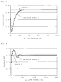
- the evaluation result is given in FIG. 6 .
- the reflection rate with respect to the variation in the SOI layer thickness did not vary but stayed constant.
- the reflection rate with respect to the variation in the SOI layer thickness varied widely.
- the method for designing an SOI wafer and the method for manufacturing an SOI wafer of the present invention realize design and manufacture of the suitable SOI wafer for photolithography, and when the SOI wafer designed and manufactured by the invention is used in the photolithography operation, the variation in the reflection rate of the exposure light due to the variation in the SOI layer thickness can be inhibited and the variation in the exposure state of the resist can be thereby inhibited.
- the SOI wafer also enables pattern formation with high precision.
- Example 2 The conditions of the wavelength ⁇ of the exposure light and the buried insulator layer thickness designed on the basis of the wavelength ⁇ in Example 1 were changed to evaluate the reflection rate in the same manner as in Example 1 (See Table 1).
- the wavelength ⁇ was 248 nm and the buried insulator layer thickness was 164.5 nm.
- Example 3 the wavelength ⁇ was 365 nm and the buried insulator layer thickness was 123.8 nm.
- Example 4 the wavelength ⁇ was 436 nm and the buried insulator layer thickness was 148.6 nm.
- the exposure state of the photoresist applied to the surface of the SOI wafer varies according to a position in a plane of the SOI layer when there is thickness distribution in the plane of the SOI layer, and this causes the difference in the developed resist pattern after exposure from the design pattern.
Abstract
Description
- The present invention relates to a method for designing and manufacturing an SOI wafer having an SOI layer formed on a buried insulator layer, and more particularly to a method for designing and manufacturing an SOI wafer suitable for photolithography that is to be performed after manufacturing.
- In recent years, SOI wafers have been used in device fabrication as semiconductor substrates having a multilayer film structure. For example, various devices, such as CPUs, logics, memories, physical sensors related to MEMS (Micro-Electro-Mechanical-Systems), biosensors, and RF devices, are fabricated by using SOI wafers.
- As methods for fabricating the SOI wafers, wafer bonding methods and a SIMOX method are generally known. An ion implantation delamination method (also referred to as the SMART-CUT (a registered trademark) method), which is one of the wafer bonding methods, is proposed in
Patent Document 1. In this method, an oxide film is formed on at least one of two silicon wafers, at least one of hydrogen ions and rare gas ions are implanted into a main surface of one of the wafers (a bond wafer) to form an ion-implanted layer in the interior of the wafer. The ion-implanted surface is then brought into close contact with a main surface of the other silicon wafer through the oxide film and the resultant wafer is then delaminated at the ion-implanted layer by performing a heat treatment at a temperature in the range of 300°C to 600°C, or more than that. The ion implantation delamination method has an advantage in that an SOI wafer having a thin SOI layer with a film thickness uniformity of ±10 nm or less can be readily fabricated and an advantage in that the delaminated bond wafer can be reused several times to reduce cost. - On the other hand, in the SIMOX method, high concentration oxygen ions are implanted into the interior of a silicon wafer to form an oxygen ion-implanted layer, a buried oxide film (a BOX layer) is then formed in the silicon wafer by performing an annealing process at a high temperature of approximately 1300°C, and a layer of its surface side is used as the SOI layer.
- A device pattern is then formed on the SOI wafer fabricated in the above manner. In this case, the feature size of pattern exhibits a wide range of pattern sizes from a relatively large size pattern for used in MEMS, RF devices and the like to a fine pattern for used in the latest CPUs, logics, memories and the like that have been significantly shrunken. Photolithography, which is one of the most important processes used for pattern formation in manufacture of various devices, has been used to form device patterns of various design rules.
- In accordance with the feature size and so on, a wavelength from a visible light region to a deep ultraviolet light (DUV) region is used as the wavelength of an exposure light utilized for a photolithography operation. More specifically, the exposure light wavelength used herein is changed according to the design rules and so on. For example, in the case of formation of a relatively large size pattern such as the above mentioned MEMS, a mercury lamp having a wavelength of 436 nm or 365 nm is used. An excimer laser having a wavelength of 248 nm or 193 nm is used for the latest CPUs, logics, and memories, for exmaple. It can be thought that an extreme ultraviolet light (EUV) having a wavelength of 13.5 nm will be used as the exposure light in future.
- For the purpose of improving line width uniformity of an image of the pattern exposed to a light on the wafer,
Patent Document 2 discloses an exposing device that is provided with a digital micro device as a reflection element array including a plurality of mirror elements that are each operable to control the reflection direction of an illumination light and controlling illumination distribution by adjusting reflection angles of the mirror elements separately from each other.Patent Document 2 also discloses use of an exposure light wavelength of 248 nm or 193 nm and use of the SOI wafer as a wafer subjected to photolithography. -
- Patent Document 1:Japanese Unexamined Patent publication (Kokai) No.
H05-211128 - Patent Document 2:Pamphlet of International Publication No.
WO2006/085626 - In the above-described photolithography operation in a device manufacturing process, there has been a problem in that the reflection rate of the exposure light varies widely due to variation in the SOI layer thickness in a plane of the SOI wafer and the intensity of exposure to a resist thereby varies so that unevenness of exposure is created. As a result, pattern blurring and pattern shift are created in a developed pattern, thereby resulting in a difference in the developed pattern from the corresponding designed pattern. A difference from design may also be created in pattern formation of the SOI wafer, which is performed by subsequent steps such as etching, film formation, and ion implantation, thereby resulting in variation in device electric characteristics.
- The present invention was accomplished in view of the above-described problems, and its object is to provide a method for designing an SOI wafer and a method for manufacturing an SOI wafer that enable the variation in the reflection rate of the exposure light due to the variation in the SOI layer thickness of the SOI wafer and hence variation in the exposure state of a resist to be inhibited in a photolithography operation.
- To achieve this object, the present invention provides a method for designing an SOI wafer that has an SOI layer formed on a buried insulator layer and is suitable for photolithography with an exposure light having a wavelength λ, the method comprising designing a thickness of the buried insulator layer of the SOI wafer on the basis of the wavelength λ of the exposure light.
- When the thickness of the buried insulator layer of the SOI wafer is designed on the basis of the wavelength λ of the exposure light as above, an SOI wafer can be designed which enables inhibition of the variation in the reflection rate of the exposure light due to the variation in the SOI layer thickness and hence inhibition of the variation in the exposure state of the resist when the photolithography operation is performed on the SOI wafer and enables pattern formation with high precision.
- In this method, the thickness of the buried insulator layer of the SOI wafer can be designed as a thickness d satisfying an expression d=(1/2)×(λ/n)×A, wherein d represents the thickness of the buried insulator layer, n represents a refractive index of the buried insulator layer, and A represents an arbitrary positive integer.
When the thickness of the buried insulator layer of the SOI wafer is designed as a thickness d satisfying an expression d=(1/2)×(λ/n)×A, wherein d represents the thickness of the buried insulator layer, n represents a refractive index of the buried insulator layer, and A represents an arbitrary positive integer as above, the thickness of the buried insulator layer of the SOI wafer can be concretely designed on the basis of the wavelength λ of the exposure light utilized for the photolithography operation, and the SOI wafer can be designed which enables inhibition of the variation in the reflection rate of the exposure light due to the variation in the SOI layer thickness and hence inhibition of the variation in the exposure state of the resist when the photolithography operation is performed on the SOI wafer. - In the method, the buried insulator layer can be any one of a silicon oxide film, a silicon nitride film, and a silicon oxynitride film, or a laminated insulator layer formed as a multilayer thereof.
Even when various insulator films, such as any one of a silicon oxide film, a silicon nitride film, and a silicon oxynitride film, or a laminated insulator layer formed as a multilayer thereof, are used as the buried insulator layer, the SOI wafer can be designed which enables inhibition of the variation in the reflection rate of the exposure light due to the variation in the SOI layer thickness and hence inhibition of the variation in the exposure state of the resist in the photolithography operation in accordance with the present invention. - Furthermore, the present invention provides a method for manufacturing an SOI wafer that has an SOI layer formed on a buried insulator layer and is suitable for photolithography with an exposure light having a wavelength λ, the method comprising the steps of: designing a thickness of the buried insulator layer of the SOI wafer on the basis of the wavelength λ of the exposure light utilized for the photolithography that is to be performed on the SOI wafer after manufacturing; and fabricating the SOI wafer that has the SOI layer formed on the buried insulator layer having the designed thickness.
- With the manufacturing method including the steps of: designing a thickness of the buried insulator layer of the SOI wafer on the basis of the wavelength λ of the exposure light utilized for the photolithography that is to be performed on the SOI wafer after manufacturing; and fabricating the SOI wafer that has the SOI layer formed on the buried insulator layer having the designed thickness as above, the SOI wafer can be manufactured which enables inhibition of the variation in the reflection rate of the exposure light due to the variation in the SOI layer thickness and hence inhibition of the variation in the exposure state of the resist when the photolithography operation is performed on the SOI wafer and enables pattern formation with high precision.
- In the manufacturing method, the thickness of the buried insulator layer of the SOI wafer can be designed as a thickness d satisfying an expression d=(1/2)×(λ/n)×A, wherein d represents the thickness of the buried insulator layer, n represents a refractive index of the buried insulator layer, and A represents an arbitrary positive integer.
When the thickness of the buried insulator layer of the SOI wafer is designed as a thickness d satisfying an expression d=(1/2)×(λ/n)×A, wherein d represents the thickness of the buried insulator layer, n represents a refractive index of the buried insulator layer, and A represents an arbitrary positive integer as above, the thickness of the buried insulator layer of the SOI wafer can be concretely designed on the basis of the wavelength λ of the exposure light utilized for the photolithography operation, and the SOI wafer can be manufactured which enables inhibition of the variation in the reflection rate of the exposure light due to the variation in the SOI layer thickness and hence inhibition of the variation in the exposure state of the resist when the photolithography operation is performed on the SOI wafer. - In the manufacturing method, the buried insulator layer can be any one of a silicon oxide film, a silicon nitride film, and a silicon oxynitride film, or a laminated insulator layer formed as a multilayer thereof.
Even when various insulator films, such as any one of a silicon oxide film, a silicon nitride film, and a silicon oxynitride film, or a laminated insulator layer formed as a multilayer thereof, are used as the buried insulator layer, the SOI wafer can be manufactured which enables inhibition of the variation in the reflection rate of the exposure light due to the variation in the SOI layer thickness and hence inhibition of the variation in the exposure state of the resist in the photolithography operation in accordance with the present invention. - In the inventive method for manufacturing an SOI wafer that has an SOI layer formed on a buried insulator layer and is suitable for photolithography with an exposure light having a wavelength λ, at least the steps of: designing the thickness of the buried insulator layer of the SOI wafer on the basis of the wavelength λ of the exposure light utilized for the photolithography operation that is to be performed on the SOI wafer after manufacturing; and fabricating the SOI wafer that has the SOI layer formed on the buried insulator layer having the designed thickness are included. The method can therefore manufacture the SOI wafer which enables inhibition of the variation in the reflection rate of the exposure light due to the variation in the SOI layer thickness and hence inhibition of the variation in the exposure state of the resist when the photolithography operation is performed on the SOI wafer and enables pattern formation with high precision. In addition, the reflection rate of the light to which the SOI wafer manufactured by the present invention is exposed can be made to be equivalent to that in the case of a bulk silicon (a silicon single crystal). The present invention thus has also an advantage in that photolithography conditions (the thickness of the resist, the thickness of a film for preventing reflection, exposure conditions and so on) for the bulk silicon can be used without alteration.
-
-
FIG. 1 is a diagram showing the result of a simulation of a relation among the SOI layer thickness, the buried insulator layer thickness, and the reflection rate in the case of a wavelength of 193 nm; -
FIG. 2 is a diagram showing the result of a simulation of a relation among the SOI layer thickness, the buried insulator layer thickness, and the reflection rate in the case of a wavelength of 248 nm; -
FIG. 3 is a diagram showing the result of a simulation of a relation among the SOI layer thickness, the buried insulator layer thickness, and the reflection rate in the case of a wavelength of 365 nm; -
FIG. 4 is a diagram showing the result of a simulation of a relation among the SOI layer thickness, the buried insulator layer thickness, and the reflection rate in the case of a wavelength of 436 nm; -
FIG. 5 is a diagram showing the result of measurement of the reflection rate with respect to the variation in the SOI layer thickness when being exposed to an ArF laser having a wavelength of 193 nm; -
FIG. 6 is a diagram showing the results of Example 1 and Comparative Example 1; -
FIG. 7 is a diagram showing the results of Example 2 and Comparative Example 2; -
FIG. 8 is a diagram showing the results of Example 3 and Comparative Example 3; -
FIG. 9 is a diagram showing the results of Example 4 and Comparative Example 4; and -
FIG. 10 is a schematic view showing an example of an SOI wafer being designed and manufactured by the method for designing and manufacturing an SOI wafer of the present invention. - Hereinafter, embodiments of the present invention will be described, but the present invention is not limited to these embodiments.
Conventionally, in the photolithography operation in a device fabrication process, there has been a problem in that the reflection rate of the exposure light varies widely due to the variation in the SOI layer thickness in a plane of the SOI wafer and the intensity of exposure to the resist thereby varies so that unevenness of exposure is created. As a result, a difference in the developed resist pattern from the corresponding designed pattern may be created and a difference from design may also be created in pattern formation of the SOI wafer, which is performed by subsequent steps such as etching, film formation, and ion implantation, thereby resulting in variation in device electric characteristics. - In view of this, the present inventor repeatedly and keenly conducted studies to solve the problem. The present inventor focused attention on the wavelength of the exposure light and the thickness of the buried insulator layer and simulated the relation between the SOI layer thickness and the reflection rate of the exposure light when the wavelength of the exposure light and the buried insulator layer thickness are changed.
-
FIG. 1 shows the result of the simulation of the relation between the reflection rate of the exposure light and the SOI layer thickness when SOI wafers each having a different buried insulator layer thickness are exposed to an ArF laser having a wavelength λ of 193 nm. The variation in the reflection rate is represented by a shade of color inFIG. 1 and a color closer to white exhibits a higher reflection rate.
It can be seen from the relation among the buried insulator layer thickness, the SOI layer thickness, and the reflection rate inFIG. 1 that the reflection rate does not vary (the color exhibiting the reflection rate does not vary) with respect to the variation in the SOI layer thickness when the buried insulator layer thickness is approximately 62 nm, 124 nm, and 186 nm. -
FIG. 5 shows the result of measurement of the reflection rate with respect to the variation in the SOI layer thickness when an SOI wafer having a buried insulator layer thickness of 145 nm is exposed to the ArF laser having a wavelength of 193 nm.
As shown inFIG. 5 , when the SOI layer thickness is equal to or less than 30 nm, the reflection rate varies widely due to the variation in the SOI layer thickness. When the photolithography operation is performed with the ArF laser on an SOI wafer having a SOI layer thickness of 30 nm or less, the exposure state of a photoresist applied to the surface of the SOI wafer therefore varies according to a position in a plane of the SOI layer when there is thickness distribution in the plane of the SOI layer, and this causes the difference in the developed resist pattern after exposure from the designed pattern. As a result, the variation in characteristics of devices being fabricated is induced. - The present inventor thought on the basis of these results that selecting a film thickness that is properly designed for the wavelength λ of the exposure light utilized for resist exposure in the photolithography operation as the thickness of the buried insulator layer of the SOI wafer enables the variation in the reflection rate to be avoided even though the SOI layer thickness varies. The present inventor further conducted simulations and experiments in various conditions and carefully examined them, thereby bringing the present invention to completion.
-
FIG. 10 shows a schematic view of an example of the SOI wafer being designed and manufactured by the method for designing an SOI wafer and the method for manufacturing an SOI wafer of the present invention. As shown inFIG. 10 , in theSOI wafer 10, theSOI layer 1 is formed on the buriedinsulator layer 2 on thebase wafer 3, which is a supporting substrate.
A wavelength in the range from the visible light region to the DUV region is used as the wavelength of the exposure light utilized for the photolithography operation being performed on theSOI wafer 10. The wavelength is appropriately determined according to the feature size on theSOI wafer 10 and so on. - In the method for designing an SOI wafer of the present invention, the thickness of the buried insulator layer of the SOI wafer is designed on the basis of the wavelength λ of the exposure light such that the variation in the reflection rate of the exposure light due to the variation in the SOI layer thickness is inhibited to design an SOI wafer suitable for the photolithography with the exposure light having the wavelength λ.
More specifically, the buried insulator layer thickness can be designed as a thickness d satisfying an expression d=(1/2)×(λ/n)×A, wherein d represents the thickness of the buried insulator layer, n represents the refractive index of the buried insulator layer, and A represents an arbitrary positive integer. - Designing the thickness of the buried insulator layer of the SOI wafer in this manner realizes design of the SOI wafer that enables inhibit of the variation in the reflection rate of the exposure light due to the variation in the SOI layer thickness and hence inhibit of the variation in the exposure state of the resist when the photolithography operation is performed on the SOI wafer and enables pattern formation with high precision.
- The results of the simulations of the relation between the SOI layer thickness and the reflection rate of the exposure light with respect to the buried insulator layer thickness when the SOI wafers were exposed to the exposure light having a wavelength λ are given in
FIGS. 1 to 4 and Table 1. In the simulations conducted herein, silicon wafers were used as the base wafers, silicon oxide films were used as the buried insulator layers. The refractive indexes of the buried insulator layers were given in Table 1.
As described above,FIG. 1 shows the simulation result when the ArF laser having a wavelength λ of 193 nm was used. As shown inFIG. 1 , the variation in the reflection rate with respect to the variation in the SOI layer thickness is substantially eliminated when the buried insulator layer thickness is approximately a positive multiple of 62 nm. Here, the positive multiple of 62 nm is equal to a value obtained by the expression (1/2)×(λ/n)×A. -
FIG. 2 shows the simulation result when a KrF laser having a wavelength λ of 248 nm was used. As shown inFIG. 2 , the variation in the reflection rate with respect to the variation in the SOI layer thickness is substantially eliminated when the buried insulator layer thickness is approximately a positive multiple of 82.2 nm.
FIG. 3 shows the simulation result when i-line of a mercury lamp having a wavelength λ of 365 nm was used. As shown inFIG. 3 , the variation in the reflection rate with respect to the variation in the SOI layer thickness is substantially eliminated when the buried insulator layer thickness is approximately a positive multiple of 123.8 nm.
FIG. 4 shows the simulation result when g-line of a mercury lamp having a wavelength λ of 436 nm was used. As shown inFIG. 4 , the variation in the reflection rate with respect to the variation in the SOI layer thickness is substantially eliminated when the buried insulator layer thickness is approximately a positive multiple of 148.6 nm.
When using EUV having a wavelength λ of 13.5 nm (not shown), the variation in the reflection rate with respect to the variation in the SOI layer thickness was substantially eliminated when the buried insulator layer thickness was approximately a positive multiple of 6.9 nm. - Table 1 summarizes the above results. As shown in the results, designing the buried insulator layer thickness d so as to satisfy the expression d=(1/2)×(λ/n)×A ensures a constant reflection rate of the exposure light without being affected by the variation in the SOI layer thickness, and the constant reflection rate can be made to be equivalent to a reflection rate in a state where the buried insulator layer thickness is zero, i.e., in a state where a bulk silicon is used.
-
(Table 1) SIMULATION 1SIMULATION 2SIMULATION 3SIMULATION 4SIMULATION 5WAVELENGTH λ OF EXPOSURE LIGHT (nm) 193 248 365 436 13.5 REFRACTIVE INDEX OF BURIED INSULATOR LAYER 1.5628 1.5086 1.4746 1.4667 0.9765 λ/2n 62 82.2 123.8 148.6 6.9 - In the method, the buried insulator layer can be any one of a silicon oxide film, a silicon nitride film, and a silicon oxynitride film, or a laminated insulator layer formed as a multilayer thereof.
When the buried insulator layer is the silicon nitride film or silicon oxynitride film as above, the buried insulator layer thickness may be designed by using the refractive index of the buried insulator layer as well as the silicon oxide film.
In the case of the laminated insulator layer formed of a plurality of buried insulator layers, the thicknesses of the buried insulator layers may be each designed such that the product (dxn) of the buried insulator layer thickness and its refractive index is calculated at each buried insulator layer in the laminated insulator layer and the sum of the products of all layers satisfies the expression (1/2)×λ×A. For example, when the laminated insulator layer has two layers, it may be designed so as to satisfy an expression d1×n1+d2×n2=(1/2)×λ×A, wherein d1 and n1 represent the thickness and refractive index of a first buried insulator layer respectively and d2 and n2 represent the thickness and refractive index of a second buried insulator layer respectively. - The present invention realizes design of a suitable SOI wafer for photolithography by which the variation in the reflection rate of the exposure light due to the variation in the SOI layer thickness can be inhibited in the photolithography operation and the variation in the exposure state of the resist can be thereby inhibited, even when various buried insulator layers are used as described above.
- Next, the method for manufacturing an SOI wafer of the present invention will be described.
First, the thickness of the buried insulator layer of the SOI wafer is designed on the basis of the wavelength λ of the exposure light utilized for photolithography that is to be performed on the SOI wafer after manufacturing such that the variation in the reflection rate of the exposure light due to the variation in the SOI layer thickness is inhibited, in the same manner as the above-described method for designing an SOI wafer of the present invention. - More specifically, the buried insulator layer thickness can be designed as a thickness d satisfying the expression d=(1/2)×(λ/n)×A, wherein d represents the thickness of the buried insulator layer, n represents the refractive index of the buried insulator layer, and A represents an arbitrary positive integer.
Next, theSOI wafer 10 having theSOI layer 1 formed on the buriedinsulator layer 2 on thebase wafer 3, which is a supporting substrate, is fabricated as shown inFIG. 10 . In the fabrication, the thickness of the buriedinsulator layer 2 is the designed thickness. - The
SOI wafer 10 can be fabricated, for example, by the bonding method in which two silicon single crystal wafers are prepared for thebase wafer 3 and the bond wafer, the buriedinsulator layer 2 having the above designed thickness is formed on at least one of the wafers, thebase wafer 3 is bonded to the bond wafer, and the bond wafer is thinned. - The thinning step for forming the
SOI layer 1 of theSOI wafer 10 can be performed by grinding and polishing, or the ion implantation delamination method. The ion implantation delamination method is a technique for obtaining an SOI wafer, for example, as follows: a silicon oxide film is formed on at least one of two silicon single crystal wafers; at least one of hydrogen ions and rare gas ions are implanted from the surface of one of the wafers (the bond wafer) to form a micro bubble layer (an enclosed layer) at the close vicinity of the surface in the interior of the wafer; the ion-implanted surface of the bond wafer is then brought into close contact with the other wafer (the base wafer) through the silicon oxide film; a heat treatment (a delamination heat treatment) is then performed to delaminate the bond wafer as a thin film such that the micro bubble layer becomes a cleavage plane (a delaminated plane); and a heat treatment (a bonding heat treatment) is further performed to firmly bond the two silicon single crystal wafers together. An SOI wafer having a thin SOI layer with very high thickness uniformity can be obtained with relative ease by the ion implantation delamination method.
The ion implantation delamination method enables easy and highly accurate control of the thickness of the SOI layer and the BOX layer and is particularly preferable to be used in the method for manufacturing an SOI wafer of the present invention. - Various heat treatments may be then applied according to the SOI wafer being fabricated.
Manufacturing the SOI wafer in this manner realizes manufacture of the suitable SOI wafer for photolithography that enables inhibition of the variation in the reflection rate of the exposure light due to the variation in the SOI layer thickness and hence inhibition of the variation in the exposure state of the resist when the photolithography operation is performed on the SOI wafer and enables pattern formation with high precision. As a result, variation in device patterns formed by developing after exposure in the photolithography operation or by subsequent processes (e.g., etching, film formation, and ion implantation) can be substantially eliminated, thereby achieving device patterns as designed. - Moreover, since the reflection rate can be made to be equivalent to a reflection rate in a state where a bulk silicon (or a bulk silicon on which a film identical to that formed on the SOI surface is formed) is used, photolithography conditions such as thickness design of a film used in the photolithography operation, e.g., a resist film, a film for preventing reflection, and a topcoat film (in the case of immersion photolithography) can be identical to those used for the bulk silicon, and this enables simplification of the photolithography.
- In the method, the buried insulator layer can be any one of a silicon oxide film, a silicon nitride film, and a silicon oxynitride film, or a laminated insulator layer formed as a multilayer thereof.
When the buried insulator layer is the silicon nitride film or silicon oxynitride film, the buried insulator layer thickness may be designed by using the refractive index of the buried insulator layer as well as the silicon oxide film. - As described above, in the case of the laminated insulator layer formed of a plurality of buried insulator layers, the thicknesses of the buried insulator layers may be each designed such that the product (dxn) of the buried insulator layer thickness and its refractive index is calculated at each buried insulator layer in the laminated insulator layer and the sum of the products of all layers satisfies the expression (1/2)×λ×A.
- The present invention realizes manufacture of the suitable SOI wafer for photolithography by which the variation in the reflection rate of the exposure light due to the variation in the SOI layer thickness can be inhibited in the photolithography operation and the variation in the exposure state of the resist can be thereby inhibited, even when various buried insulator layers are used as described above.
- In the embodiments described above, the silicon oxide film, the silicon nitride film, and the silicon oxynitride film are exemplified as the buried
insulator layer 2. In the present invention, however, insulator films made of high permittivity materials (high-k films) such as HfO2, ZrO2, La2O3, and TiO2 can also be employed. - The present invention will be more specifically described below with reference to Examples and Comparative Examples, but the present invention is not limited these examples.
- An SOI wafer suitable for photolithography with an exposure light having a wavelength λ was manufactured by the method for designing an SOI wafer and the method for manufacturing an SOI wafer of the present invention. The reflection rate with respect to the variation in the SOI layer thickness was evaluated when the manufactured SOI wafer was exposed to the exposure light having the wavelength λ. In Example 1, the wavelength λ of the exposure light was 193 nm, and the buried insulator layer thickness designed on the basis of the wavelength λ was 124 nm (See Table 1).
- The evaluation result is given in
FIG. 6 . Referring toFIG. 6 , it can be seen that the reflection rate with respect to the variation in the SOI layer thickness did not vary but stayed constant. On the other hand, it can be seen that, in the later-described Comparative Example 1, the reflection rate with respect to the variation in the SOI layer thickness varied widely.
It can be accordingly confirmed that the method for designing an SOI wafer and the method for manufacturing an SOI wafer of the present invention realize design and manufacture of the suitable SOI wafer for photolithography, and when the SOI wafer designed and manufactured by the invention is used in the photolithography operation, the variation in the reflection rate of the exposure light due to the variation in the SOI layer thickness can be inhibited and the variation in the exposure state of the resist can be thereby inhibited. The SOI wafer also enables pattern formation with high precision. - The conditions of the wavelength λ of the exposure light and the buried insulator layer thickness designed on the basis of the wavelength λ in Example 1 were changed to evaluate the reflection rate in the same manner as in Example 1 (See Table 1). In Example 2, the wavelength λ was 248 nm and the buried insulator layer thickness was 164.5 nm. In Example 3, the wavelength λ was 365 nm and the buried insulator layer thickness was 123.8 nm. In Example 4, the wavelength λ was 436 nm and the buried insulator layer thickness was 148.6 nm.
- The evaluation results are given in
FIGS. 7 to 9 . Referring toFIGS. 7 to 9 , in all of these examples, the reflection rate with respect to the variation in the SOI layer thickness did not vary but stayed constant. The results exhibited the same tendency as Example 1. - An SOI wafer was manufactured in the same manner as Examples 1 to 4 except that the buried insulator layer thickness d was designed to be a thickness not satisfying the expression d=(1/2)×(λ/n)×A, and the reflection rate was evaluated in the same manner as Example 1. In Comparative Example 1, the buried insulator layer thickness was 145 nm. In Comparative Examples 2 to 4, the buried insulator layer thickness was 200 nm.
The results are given inFIGS. 6 to 9 . Referring toFIGS. 6 to 9 , it can be seen that, in Comparative Examples 1 to 4, the reflection rate with respect to the variation in the SOI layer thickness varied widely. - Therefore, when the photolithography operation is performed on the SOI wafer having the buried insulator layer thickness not satisfying (1/2)×(λ/n)×A, the exposure state of the photoresist applied to the surface of the SOI wafer varies according to a position in a plane of the SOI layer when there is thickness distribution in the plane of the SOI layer, and this causes the difference in the developed resist pattern after exposure from the design pattern.
- It is to be noted that the present invention is not limited to the foregoing embodiment. The embodiment is just an exemplification, and any examples that have substantially the same feature and demonstrate the same functions and effects as those in the technical concept described in claims of the present invention are included in the technical scope of the present invention.
Claims (6)
- A method for designing an SOI wafer that has an SOI layer formed on a buried insulator layer and is suitable for photolithography with an exposure light having a wavelength λ, the method comprising
designing a thickness of the buried insulator layer of the SOI wafer on the basis of the wavelength λ of the exposure light. - The method for designing an SOI wafer according to claim 1, wherein the thickness of the buried insulator layer of the SOI wafer is designed as a thickness d satisfying an expression d=(1/2)×(λ/n)×A, wherein d represents the thickness of the buried insulator layer, n represents a refractive index of the buried insulator layer, and A represents an arbitrary positive integer.
- The method for designing an SOI wafer according to claim 1 or claim 2, wherein the buried insulator layer is any one of a silicon oxide film, a silicon nitride film, and a silicon oxynitride film, or a laminated insulator layer formed as a multilayer thereof.
- A method for manufacturing an SOI wafer that has an SOI layer formed on a buried insulator layer and is suitable for photolithography with an exposure light having a wavelength λ, the method comprising the steps of:designing a thickness of the buried insulator layer of the SOI wafer on the basis of the wavelength λ of the exposure light utilized for the photolithography that is to be performed on the SOI wafer after manufacturing; andfabricating the SOI wafer that has the SOI layer formed on the buried insulator layer having the designed thickness.
- The method for manufacturing an SOI wafer according to claim 4, wherein the thickness of the buried insulator layer of the SOI wafer is designed as a thickness d satisfying an expression d=(1/2)×(λ/n)×A, wherein d represents the thickness of the buried insulator layer, n represents a refractive index of the buried insulator layer, and A represents an arbitrary positive integer.
- The method for manufacturing an SOI wafer according to claim 4 or claim 5, wherein the buried insulator layer is any one of a silicon oxide film, a silicon nitride film, and a silicon oxynitride film, or a laminated insulator layer formed as a multilayer thereof.
Applications Claiming Priority (2)
| Application Number | Priority Date | Filing Date | Title |
|---|---|---|---|
| JP2010047885A JP5387450B2 (en) | 2010-03-04 | 2010-03-04 | Design method and manufacturing method of SOI wafer |
| PCT/JP2011/000598 WO2011108188A1 (en) | 2010-03-04 | 2011-02-03 | Method for producing and method for designing soi wafer |
Publications (3)
| Publication Number | Publication Date |
|---|---|
| EP2544235A1 true EP2544235A1 (en) | 2013-01-09 |
| EP2544235A4 EP2544235A4 (en) | 2013-12-04 |
| EP2544235B1 EP2544235B1 (en) | 2017-08-02 |
Family
ID=44541859
Family Applications (1)
| Application Number | Title | Priority Date | Filing Date |
|---|---|---|---|
| EP11750302.9A Active EP2544235B1 (en) | 2010-03-04 | 2011-02-03 | Method for producing an soi wafer |
Country Status (7)
| Country | Link |
|---|---|
| US (1) | US8741741B2 (en) |
| EP (1) | EP2544235B1 (en) |
| JP (1) | JP5387450B2 (en) |
| KR (1) | KR101642970B1 (en) |
| CN (1) | CN102782851B (en) |
| SG (1) | SG183290A1 (en) |
| WO (1) | WO2011108188A1 (en) |
Families Citing this family (2)
| Publication number | Priority date | Publication date | Assignee | Title |
|---|---|---|---|---|
| JP5387451B2 (en) * | 2010-03-04 | 2014-01-15 | 信越半導体株式会社 | Design method and manufacturing method of SOI wafer |
| JP6107353B2 (en) * | 2013-04-12 | 2017-04-05 | 株式会社島津製作所 | Surface treatment status monitoring device |
Citations (3)
| Publication number | Priority date | Publication date | Assignee | Title |
|---|---|---|---|---|
| EP1016930A1 (en) * | 1998-12-28 | 2000-07-05 | Infineon Technologies North America Corp. | Bottom antireflective layer operating in destructive interference and absorption modes |
| US6428894B1 (en) * | 1997-06-04 | 2002-08-06 | International Business Machines Corporation | Tunable and removable plasma deposited antireflective coatings |
| EP1806769A1 (en) * | 2004-09-13 | 2007-07-11 | Shin-Etsu Handotai Company Limited | Soi wafer manufacturing method and soi wafer |
Family Cites Families (12)
| Publication number | Priority date | Publication date | Assignee | Title |
|---|---|---|---|---|
| FR2681472B1 (en) | 1991-09-18 | 1993-10-29 | Commissariat Energie Atomique | PROCESS FOR PRODUCING THIN FILMS OF SEMICONDUCTOR MATERIAL. |
| DE69232432T2 (en) | 1991-11-20 | 2002-07-18 | Canon Kk | Method of manufacturing a semiconductor device |
| JP3363496B2 (en) * | 1991-11-20 | 2003-01-08 | キヤノン株式会社 | Semiconductor device and manufacturing method thereof |
| JP2001144059A (en) * | 1999-11-17 | 2001-05-25 | Denso Corp | Method of manufacturing semiconductor device |
| JP3946470B2 (en) * | 2001-03-12 | 2007-07-18 | 株式会社デンソー | Method for measuring thickness of semiconductor layer and method for manufacturing semiconductor substrate |
| DE10339988B4 (en) | 2003-08-29 | 2008-06-12 | Advanced Micro Devices, Inc., Sunnyvale | Method for producing an antireflecting layer |
| EP1658635A1 (en) * | 2003-08-29 | 2006-05-24 | Advanced Micro Devices, Inc. | A method of forming a TEOS cap layer at low temperature and reduced deposition rate |
| JP4826994B2 (en) * | 2004-09-13 | 2011-11-30 | 信越半導体株式会社 | Manufacturing method of SOI wafer |
| WO2006085626A1 (en) | 2005-02-14 | 2006-08-17 | Nikon Corporation | Exposure method and system, and method for fabricating device |
| JP5003322B2 (en) * | 2007-07-09 | 2012-08-15 | 信越半導体株式会社 | SOI wafer evaluation method |
| JP5135935B2 (en) * | 2007-07-27 | 2013-02-06 | 信越半導体株式会社 | Manufacturing method of bonded wafer |
| CN101308230A (en) * | 2008-07-03 | 2008-11-19 | 中国科学院上海微系统与信息技术研究所 | Isolator silicon based three-dimensional wedge-shaped spot-size converter and method for making same |
-
2010
- 2010-03-04 JP JP2010047885A patent/JP5387450B2/en active Active
-
2011
- 2011-02-03 SG SG2012059796A patent/SG183290A1/en unknown
- 2011-02-03 US US13/576,889 patent/US8741741B2/en active Active
- 2011-02-03 WO PCT/JP2011/000598 patent/WO2011108188A1/en active Application Filing
- 2011-02-03 CN CN201180012260.5A patent/CN102782851B/en active Active
- 2011-02-03 EP EP11750302.9A patent/EP2544235B1/en active Active
- 2011-02-03 KR KR1020127022865A patent/KR101642970B1/en active IP Right Grant
Patent Citations (3)
| Publication number | Priority date | Publication date | Assignee | Title |
|---|---|---|---|---|
| US6428894B1 (en) * | 1997-06-04 | 2002-08-06 | International Business Machines Corporation | Tunable and removable plasma deposited antireflective coatings |
| EP1016930A1 (en) * | 1998-12-28 | 2000-07-05 | Infineon Technologies North America Corp. | Bottom antireflective layer operating in destructive interference and absorption modes |
| EP1806769A1 (en) * | 2004-09-13 | 2007-07-11 | Shin-Etsu Handotai Company Limited | Soi wafer manufacturing method and soi wafer |
Non-Patent Citations (1)
| Title |
|---|
| See also references of WO2011108188A1 * |
Also Published As
| Publication number | Publication date |
|---|---|
| JP2011187474A (en) | 2011-09-22 |
| US20120295424A1 (en) | 2012-11-22 |
| KR20120121909A (en) | 2012-11-06 |
| EP2544235A4 (en) | 2013-12-04 |
| CN102782851B (en) | 2015-06-17 |
| WO2011108188A1 (en) | 2011-09-09 |
| SG183290A1 (en) | 2012-09-27 |
| US8741741B2 (en) | 2014-06-03 |
| EP2544235B1 (en) | 2017-08-02 |
| KR101642970B1 (en) | 2016-07-26 |
| JP5387450B2 (en) | 2014-01-15 |
| CN102782851A (en) | 2012-11-14 |
Similar Documents
| Publication | Publication Date | Title |
|---|---|---|
| US9612523B2 (en) | Structure and method for reflective-type mask | |
| JP6374360B2 (en) | EUV mask and manufacturing method thereof | |
| EP1785751A1 (en) | Optical element having multilayer film, and exposure apparatus having the optical element | |
| JP2006235321A (en) | Method for manufacturing transparent substrate for mask blank, method for manufacturing mask blank, and method for manufacturing exposure mask | |
| JP2008277541A (en) | Light-reflective mask, method of making light-reflective mask, and manufacturing method of semiconductor device | |
| US8741741B2 (en) | Method for designing SOI wafer and method for manufacturing SOI wafer | |
| US7157211B2 (en) | Method of fabricating a semiconductor device | |
| KR101642967B1 (en) | Method for producing and method for designing soi wafer | |
| JPH11352669A (en) | Exposing method and reflection type mask | |
| US9069253B2 (en) | Mask structure | |
| JP5761000B2 (en) | Method for manufacturing reflective mask blank for EUV lithography and method for manufacturing reflective mask for EUV lithography | |
| JP2008181083A (en) | Grayscale mask using smart cut (r) wafer bonding process and method for fabricating the same | |
| KR101412809B1 (en) | Method and apparatus for improving the alignment of the upper and lower layer of the lamination structure of the wafer and improving the transmittancy | |
| JP2022171587A (en) | Photomask blank, photomask, and manufacturing method of semiconductor element | |
| KR20190118325A (en) | Method of fabricating EUV lithography pellicle film | |
| JP2009246321A (en) | Soi substrate manufacturing method | |
| KR20130006748A (en) | Extreme ultra violet exposure mask and stepper including the same |
Legal Events
| Date | Code | Title | Description |
|---|---|---|---|
| PUAI | Public reference made under article 153(3) epc to a published international application that has entered the european phase |
Free format text: ORIGINAL CODE: 0009012 |
|
| 17P | Request for examination filed |
Effective date: 20120822 |
|
| AK | Designated contracting states |
Kind code of ref document: A1 Designated state(s): AL AT BE BG CH CY CZ DE DK EE ES FI FR GB GR HR HU IE IS IT LI LT LU LV MC MK MT NL NO PL PT RO RS SE SI SK SM TR |
|
| DAX | Request for extension of the european patent (deleted) | ||
| A4 | Supplementary search report drawn up and despatched |
Effective date: 20131106 |
|
| RIC1 | Information provided on ipc code assigned before grant |
Ipc: H01L 27/12 20060101AFI20131030BHEP Ipc: H01L 21/762 20060101ALI20131030BHEP |
|
| RAP1 | Party data changed (applicant data changed or rights of an application transferred) |
Owner name: SHIN-ETSU HANDOTAI CO., LTD. |
|
| 17Q | First examination report despatched |
Effective date: 20160617 |
|
| GRAP | Despatch of communication of intention to grant a patent |
Free format text: ORIGINAL CODE: EPIDOSNIGR1 |
|
| STAA | Information on the status of an ep patent application or granted ep patent |
Free format text: STATUS: GRANT OF PATENT IS INTENDED |
|
| INTG | Intention to grant announced |
Effective date: 20170224 |
|
| GRAS | Grant fee paid |
Free format text: ORIGINAL CODE: EPIDOSNIGR3 |
|
| GRAA | (expected) grant |
Free format text: ORIGINAL CODE: 0009210 |
|
| STAA | Information on the status of an ep patent application or granted ep patent |
Free format text: STATUS: THE PATENT HAS BEEN GRANTED |
|
| AK | Designated contracting states |
Kind code of ref document: B1 Designated state(s): AL AT BE BG CH CY CZ DE DK EE ES FI FR GB GR HR HU IE IS IT LI LT LU LV MC MK MT NL NO PL PT RO RS SE SI SK SM TR |
|
| REG | Reference to a national code |
Ref country code: GB Ref legal event code: FG4D |
|
| REG | Reference to a national code |
Ref country code: CH Ref legal event code: EP Ref country code: AT Ref legal event code: REF Ref document number: 915342 Country of ref document: AT Kind code of ref document: T Effective date: 20170815 |
|
| REG | Reference to a national code |
Ref country code: IE Ref legal event code: FG4D |
|
| REG | Reference to a national code |
Ref country code: DE Ref legal event code: R096 Ref document number: 602011040162 Country of ref document: DE |
|
| REG | Reference to a national code |
Ref country code: NL Ref legal event code: MP Effective date: 20170802 |
|
| REG | Reference to a national code |
Ref country code: AT Ref legal event code: MK05 Ref document number: 915342 Country of ref document: AT Kind code of ref document: T Effective date: 20170802 |
|
| REG | Reference to a national code |
Ref country code: LT Ref legal event code: MG4D |
|
| PG25 | Lapsed in a contracting state [announced via postgrant information from national office to epo] |
Ref country code: AT Free format text: LAPSE BECAUSE OF FAILURE TO SUBMIT A TRANSLATION OF THE DESCRIPTION OR TO PAY THE FEE WITHIN THE PRESCRIBED TIME-LIMIT Effective date: 20170802 Ref country code: LT Free format text: LAPSE BECAUSE OF FAILURE TO SUBMIT A TRANSLATION OF THE DESCRIPTION OR TO PAY THE FEE WITHIN THE PRESCRIBED TIME-LIMIT Effective date: 20170802 Ref country code: SE Free format text: LAPSE BECAUSE OF FAILURE TO SUBMIT A TRANSLATION OF THE DESCRIPTION OR TO PAY THE FEE WITHIN THE PRESCRIBED TIME-LIMIT Effective date: 20170802 Ref country code: NO Free format text: LAPSE BECAUSE OF FAILURE TO SUBMIT A TRANSLATION OF THE DESCRIPTION OR TO PAY THE FEE WITHIN THE PRESCRIBED TIME-LIMIT Effective date: 20171102 Ref country code: NL Free format text: LAPSE BECAUSE OF FAILURE TO SUBMIT A TRANSLATION OF THE DESCRIPTION OR TO PAY THE FEE WITHIN THE PRESCRIBED TIME-LIMIT Effective date: 20170802 Ref country code: HR Free format text: LAPSE BECAUSE OF FAILURE TO SUBMIT A TRANSLATION OF THE DESCRIPTION OR TO PAY THE FEE WITHIN THE PRESCRIBED TIME-LIMIT Effective date: 20170802 Ref country code: FI Free format text: LAPSE BECAUSE OF FAILURE TO SUBMIT A TRANSLATION OF THE DESCRIPTION OR TO PAY THE FEE WITHIN THE PRESCRIBED TIME-LIMIT Effective date: 20170802 |
|
| REG | Reference to a national code |
Ref country code: FR Ref legal event code: PLFP Year of fee payment: 8 |
|
| PG25 | Lapsed in a contracting state [announced via postgrant information from national office to epo] |
Ref country code: LV Free format text: LAPSE BECAUSE OF FAILURE TO SUBMIT A TRANSLATION OF THE DESCRIPTION OR TO PAY THE FEE WITHIN THE PRESCRIBED TIME-LIMIT Effective date: 20170802 Ref country code: IS Free format text: LAPSE BECAUSE OF FAILURE TO SUBMIT A TRANSLATION OF THE DESCRIPTION OR TO PAY THE FEE WITHIN THE PRESCRIBED TIME-LIMIT Effective date: 20171202 Ref country code: ES Free format text: LAPSE BECAUSE OF FAILURE TO SUBMIT A TRANSLATION OF THE DESCRIPTION OR TO PAY THE FEE WITHIN THE PRESCRIBED TIME-LIMIT Effective date: 20170802 Ref country code: BG Free format text: LAPSE BECAUSE OF FAILURE TO SUBMIT A TRANSLATION OF THE DESCRIPTION OR TO PAY THE FEE WITHIN THE PRESCRIBED TIME-LIMIT Effective date: 20171102 Ref country code: PL Free format text: LAPSE BECAUSE OF FAILURE TO SUBMIT A TRANSLATION OF THE DESCRIPTION OR TO PAY THE FEE WITHIN THE PRESCRIBED TIME-LIMIT Effective date: 20170802 Ref country code: GR Free format text: LAPSE BECAUSE OF FAILURE TO SUBMIT A TRANSLATION OF THE DESCRIPTION OR TO PAY THE FEE WITHIN THE PRESCRIBED TIME-LIMIT Effective date: 20171103 Ref country code: RS Free format text: LAPSE BECAUSE OF FAILURE TO SUBMIT A TRANSLATION OF THE DESCRIPTION OR TO PAY THE FEE WITHIN THE PRESCRIBED TIME-LIMIT Effective date: 20170802 |
|
| PG25 | Lapsed in a contracting state [announced via postgrant information from national office to epo] |
Ref country code: DK Free format text: LAPSE BECAUSE OF FAILURE TO SUBMIT A TRANSLATION OF THE DESCRIPTION OR TO PAY THE FEE WITHIN THE PRESCRIBED TIME-LIMIT Effective date: 20170802 Ref country code: RO Free format text: LAPSE BECAUSE OF FAILURE TO SUBMIT A TRANSLATION OF THE DESCRIPTION OR TO PAY THE FEE WITHIN THE PRESCRIBED TIME-LIMIT Effective date: 20170802 Ref country code: CZ Free format text: LAPSE BECAUSE OF FAILURE TO SUBMIT A TRANSLATION OF THE DESCRIPTION OR TO PAY THE FEE WITHIN THE PRESCRIBED TIME-LIMIT Effective date: 20170802 |
|
| REG | Reference to a national code |
Ref country code: DE Ref legal event code: R097 Ref document number: 602011040162 Country of ref document: DE |
|
| PG25 | Lapsed in a contracting state [announced via postgrant information from national office to epo] |
Ref country code: EE Free format text: LAPSE BECAUSE OF FAILURE TO SUBMIT A TRANSLATION OF THE DESCRIPTION OR TO PAY THE FEE WITHIN THE PRESCRIBED TIME-LIMIT Effective date: 20170802 Ref country code: SM Free format text: LAPSE BECAUSE OF FAILURE TO SUBMIT A TRANSLATION OF THE DESCRIPTION OR TO PAY THE FEE WITHIN THE PRESCRIBED TIME-LIMIT Effective date: 20170802 Ref country code: IT Free format text: LAPSE BECAUSE OF FAILURE TO SUBMIT A TRANSLATION OF THE DESCRIPTION OR TO PAY THE FEE WITHIN THE PRESCRIBED TIME-LIMIT Effective date: 20170802 Ref country code: SK Free format text: LAPSE BECAUSE OF FAILURE TO SUBMIT A TRANSLATION OF THE DESCRIPTION OR TO PAY THE FEE WITHIN THE PRESCRIBED TIME-LIMIT Effective date: 20170802 |
|
| PLBE | No opposition filed within time limit |
Free format text: ORIGINAL CODE: 0009261 |
|
| STAA | Information on the status of an ep patent application or granted ep patent |
Free format text: STATUS: NO OPPOSITION FILED WITHIN TIME LIMIT |
|
| 26N | No opposition filed |
Effective date: 20180503 |
|
| PG25 | Lapsed in a contracting state [announced via postgrant information from national office to epo] |
Ref country code: SI Free format text: LAPSE BECAUSE OF FAILURE TO SUBMIT A TRANSLATION OF THE DESCRIPTION OR TO PAY THE FEE WITHIN THE PRESCRIBED TIME-LIMIT Effective date: 20170802 |
|
| REG | Reference to a national code |
Ref country code: CH Ref legal event code: PL |
|
| PG25 | Lapsed in a contracting state [announced via postgrant information from national office to epo] |
Ref country code: MC Free format text: LAPSE BECAUSE OF FAILURE TO SUBMIT A TRANSLATION OF THE DESCRIPTION OR TO PAY THE FEE WITHIN THE PRESCRIBED TIME-LIMIT Effective date: 20170802 |
|
| GBPC | Gb: european patent ceased through non-payment of renewal fee |
Effective date: 20180203 |
|
| REG | Reference to a national code |
Ref country code: IE Ref legal event code: MM4A |
|
| REG | Reference to a national code |
Ref country code: BE Ref legal event code: MM Effective date: 20180228 |
|
| PG25 | Lapsed in a contracting state [announced via postgrant information from national office to epo] |
Ref country code: LI Free format text: LAPSE BECAUSE OF NON-PAYMENT OF DUE FEES Effective date: 20180228 Ref country code: LU Free format text: LAPSE BECAUSE OF NON-PAYMENT OF DUE FEES Effective date: 20180203 Ref country code: CH Free format text: LAPSE BECAUSE OF NON-PAYMENT OF DUE FEES Effective date: 20180228 |
|
| PG25 | Lapsed in a contracting state [announced via postgrant information from national office to epo] |
Ref country code: IE Free format text: LAPSE BECAUSE OF NON-PAYMENT OF DUE FEES Effective date: 20180203 |
|
| PG25 | Lapsed in a contracting state [announced via postgrant information from national office to epo] |
Ref country code: BE Free format text: LAPSE BECAUSE OF NON-PAYMENT OF DUE FEES Effective date: 20180228 Ref country code: GB Free format text: LAPSE BECAUSE OF NON-PAYMENT OF DUE FEES Effective date: 20180203 |
|
| PG25 | Lapsed in a contracting state [announced via postgrant information from national office to epo] |
Ref country code: MT Free format text: LAPSE BECAUSE OF NON-PAYMENT OF DUE FEES Effective date: 20180203 |
|
| PG25 | Lapsed in a contracting state [announced via postgrant information from national office to epo] |
Ref country code: TR Free format text: LAPSE BECAUSE OF FAILURE TO SUBMIT A TRANSLATION OF THE DESCRIPTION OR TO PAY THE FEE WITHIN THE PRESCRIBED TIME-LIMIT Effective date: 20170802 |
|
| PG25 | Lapsed in a contracting state [announced via postgrant information from national office to epo] |
Ref country code: PT Free format text: LAPSE BECAUSE OF FAILURE TO SUBMIT A TRANSLATION OF THE DESCRIPTION OR TO PAY THE FEE WITHIN THE PRESCRIBED TIME-LIMIT Effective date: 20170802 Ref country code: HU Free format text: LAPSE BECAUSE OF FAILURE TO SUBMIT A TRANSLATION OF THE DESCRIPTION OR TO PAY THE FEE WITHIN THE PRESCRIBED TIME-LIMIT; INVALID AB INITIO Effective date: 20110203 |
|
| PG25 | Lapsed in a contracting state [announced via postgrant information from national office to epo] |
Ref country code: CY Free format text: LAPSE BECAUSE OF FAILURE TO SUBMIT A TRANSLATION OF THE DESCRIPTION OR TO PAY THE FEE WITHIN THE PRESCRIBED TIME-LIMIT Effective date: 20170802 Ref country code: MK Free format text: LAPSE BECAUSE OF NON-PAYMENT OF DUE FEES Effective date: 20170802 |
|
| PG25 | Lapsed in a contracting state [announced via postgrant information from national office to epo] |
Ref country code: AL Free format text: LAPSE BECAUSE OF FAILURE TO SUBMIT A TRANSLATION OF THE DESCRIPTION OR TO PAY THE FEE WITHIN THE PRESCRIBED TIME-LIMIT Effective date: 20170802 |
|
| PGFP | Annual fee paid to national office [announced via postgrant information from national office to epo] |
Ref country code: FR Payment date: 20230110 Year of fee payment: 13 |
|
| PGFP | Annual fee paid to national office [announced via postgrant information from national office to epo] |
Ref country code: DE Payment date: 20231228 Year of fee payment: 14 |