EP2500992B1 - Electrical conector - Google Patents
Electrical conector Download PDFInfo
- Publication number
- EP2500992B1 EP2500992B1 EP11382071.6A EP11382071A EP2500992B1 EP 2500992 B1 EP2500992 B1 EP 2500992B1 EP 11382071 A EP11382071 A EP 11382071A EP 2500992 B1 EP2500992 B1 EP 2500992B1
- Authority
- EP
- European Patent Office
- Prior art keywords
- connector
- accordance
- circuit board
- contact subassembly
- printed circuit
- Prior art date
- Legal status (The legal status is an assumption and is not a legal conclusion. Google has not performed a legal analysis and makes no representation as to the accuracy of the status listed.)
- Not-in-force
Links
Images
Classifications
-
- H—ELECTRICITY
- H01—ELECTRIC ELEMENTS
- H01R—ELECTRICALLY-CONDUCTIVE CONNECTIONS; STRUCTURAL ASSOCIATIONS OF A PLURALITY OF MUTUALLY-INSULATED ELECTRICAL CONNECTING ELEMENTS; COUPLING DEVICES; CURRENT COLLECTORS
- H01R13/00—Details of coupling devices of the kinds covered by groups H01R12/70 or H01R24/00 - H01R33/00
- H01R13/66—Structural association with built-in electrical component
- H01R13/665—Structural association with built-in electrical component with built-in electronic circuit
- H01R13/6658—Structural association with built-in electrical component with built-in electronic circuit on printed circuit board
-
- H—ELECTRICITY
- H01—ELECTRIC ELEMENTS
- H01R—ELECTRICALLY-CONDUCTIVE CONNECTIONS; STRUCTURAL ASSOCIATIONS OF A PLURALITY OF MUTUALLY-INSULATED ELECTRICAL CONNECTING ELEMENTS; COUPLING DEVICES; CURRENT COLLECTORS
- H01R2107/00—Four or more poles
-
- H—ELECTRICITY
- H01—ELECTRIC ELEMENTS
- H01R—ELECTRICALLY-CONDUCTIVE CONNECTIONS; STRUCTURAL ASSOCIATIONS OF A PLURALITY OF MUTUALLY-INSULATED ELECTRICAL CONNECTING ELEMENTS; COUPLING DEVICES; CURRENT COLLECTORS
- H01R24/00—Two-part coupling devices, or either of their cooperating parts, characterised by their overall structure
- H01R24/60—Contacts spaced along planar side wall transverse to longitudinal axis of engagement
- H01R24/62—Sliding engagements with one side only, e.g. modular jack coupling devices
- H01R24/64—Sliding engagements with one side only, e.g. modular jack coupling devices for high frequency, e.g. RJ 45
Definitions
- This invention refers to an electrical connection including IDC insulation displacement contacts and a cover which includes a fixture for holding wires of a communications cable in proper position for the termination of the contacts.
- An electrical connector is known in the state of the art, for example, from American patent US5.947.761 for use in data communications systems having insulation displacement contacts IDC.
- the electrical connector receives a communications cable including a set of individually insulated wires which are set in the corresponding IDC contacts of the electrical connector.
- the electrical connector also includes a dielectric housing, a terminal insert, a contact subassembly and a wire fixture for retaining the communications cable in an appropriate position for termination of the electrical connector.
- the terminal insert includes a printed circuit board that cooperates with the IDC insulation displacement contacts, in order to electrically connect the line wires with the respective terminals.
- the contact subassembly includes a contact dielectric holder which holds a plurality of insulation displacement contacts IDC these are generally aligned in rows parallel to the back part of the electrical connector, i.e., in proximity to the part of the wire fixture for which the communications cable enters the electrical connector.
- the IDC contacts are designed to receive in each a line wire included in the communications cable.
- a wire insertion face is provided for receiving each of these wires and to plug in or subsequently connect in the posterior part of the connector proceeding to push each line wire into its respective IDC.
- the wire fixture of the cover makes a pivotal movement or a plugging movement of the line wires into the IDC contacts.
- the cover comprises connection thrusters so that in their closing movement, they push and progressively approximate each line wire, through a lever effect, to its fully plugged in position in the posterior part of the electrical connector.
- a disadvantage of the electrical connector or modular female socket is that it requires to connect an external circuit to the electrical connector to meet electrical functionalities such as to check voltage in the communications wires connected to the electrical connector and to verify the correct polarity of the connection made between the line wires and the IDC contacts or detecting presence/absence of connector at the far-end of the communication line.
- This external circuit complicates the installation practice adding time and cost as well as risk of failure while ease of application was the initial benefit of the connector.
- US7,540,760 disclosed a communication jack structure is adapted for the configuration of a plurality of wires.
- the communication jack structure includes a base and a terminal pressing member.
- the base has two rows of piercing terminals, and the terminal pressing member has plural rows of pressing slots corresponding to the piercing terminals respectively.
- Each pressing slot has an inclined wire leading portion at the opening. The wire leading portion is used for leading the wire from the opening to the bottom of the pressing slot, so as to enhance the efficiency of assembling the wire and the terminal pressing member.
- the communication jack structure adapted to electrically connect a cable and a plurality of wires is provided.
- a circuit board is provided at inner housing.
- the piercing terminals and contact terminals are respectively electrically disposed on the circuit board, and are electrically connected to each other through a plurality of connection circuits on the circuit board.
- the circuit board has two through-holes and two notches.
- An upper combination board has two latches disposed corresponding to the through-holes and two notches disposed corresponding to the notches.
- the lower combination board has notches disposed corresponding to the through-holes. The latches respectively penetrate the through-holes in the circuit board and insert in the notches in the lower combination board, so that the upper combination board and the lower combination board are engaged on two sides of the circuit board.
- the two contact terminals on the outer side are assembled on the lower combination board, and the rest of the contact terminals are assembled on the upper combination board.
- Each contact terminal has one end disposed on the circuit board and the other end bent towards the inner housing.
- the two contact terminals on the outer side respectively have their middle portions accommodated in the notches and the notches.
- the inner housing has a plurality of through-holes disposed at the bottom corresponding to the rows of the piercing terminals.
- the piercing terminals on the circuit board penetrate the inner housing via the through-holes to enter the accommodation groove, and thus the accommodation groove is provided with two rows of piercing terminals.
- This invention seeks to resolve one or more of the disadvantages described above by means of an electrical connector as described in the claims.
- One object is to supply an electrical connector in order to terminate a plurality of line wires of a communications cable including a dielectric housing; a terminal insert, a contact subassembly and a wire fixture; where a tester circuit is configured to be assembled in a terminal insert and to verify the electric connection to make between the line wires and the IDC contacts included in the contact subassembly.
- Another object is to provide an electrical circuit a type of tester or polarisation circuit connected electrically to a predetermined subset of IDC contacts, and to be assembled in a portion of a printed circuit board of the terminal insert.
- a further object is to supply an electrical circuit which comprises a switching or contact breaker element and a resistive element electrically connected in series.
- Another object is to permit the wire fixture in a closed or working position to fully cover the printed circuit assembled in the portion of the printed circuit board.
- the electrical connector including the electrical circuit is inserted without using any tool, and consequently assembly faults are prevented, such as disconnection of the polarisation circuit. Furthermore, the time required for its termination and verification is lower than an electrical connector to which it is necessary to connect an external polarisation circuit.
- the electrical connector module has a compact design, reduced and assembled in a single housing which prevents knocks, catching, and breakage of any component of the female electrical connector module.
- an electrical connector of the type female socket module knows in the state of the art from U.S. patent Nos. 5,947,761 incorporated by reference.
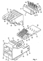
- the electrical connector includes a dielectric housing 10, a terminal insert 12, a contact subassembly 14, and a wire fixture 16.
- the housing 10 includes a receptacle portion 18 and a platform portion 20.
- the receptacle portion has a front face 22, a rear face 24, and a cavity 26 which opens into the receptacle portion though the front face.
- the cavity is configured as a receptacle for a mating modular plug.
- a pivot block 28 On top of the receptacle portion 18 is a pivot block 28 which has a pair of journals 30 extending from opposite sides thereof.
- the platform portion 20 is disposed at a rear of the receptacle portion 18.
- the platform portion includes a bottom wall 32 and side walls 34 which have openings 35, 36.
- the terminal insert 12 includes a circuit board 38 and a dielectric carrier 40 which holds a plurality of terminals 42 in an array.
- the terminals 42 have contact sections 44 which are adjacent to free ends 46, and opposite ends 48 which are electrically connected to circuit traces respectively imprinted on the printed circuit board.
- the contact subassembly 14 includes a dielectric contact holder 50 which holds a plurality of insulation displacement contacts 52.
- Each of the contacts has a split beam which defines a slot 54 that can receive a wire. Edges of the split beam on opposite sides of the slot are configured to slice the insulation jacket on a wire which is installed in the slot and to electrically engage the wire conductive core of the respective line wire.
- the contacts 52 are arranged in the holder in laterally extending rows comprising a first row 55 and a second row 56 which are spaced-apart along a longitudinal axis of the connector.
- the rows extend parallel to each other.
- the contact holder 50 includes a separator wall 58 between the two rows 55, 56 and is configured to electrically insulate the IDC contacts located on each row 55, 56.
- the contact subassembly 14 includes a horizontal U-shaped aperture opened through the lower wall of the subassembly 14 and distanced from the furthest row of a wall 51, which faces a rear face 24 of the receptacle portion 18 and closes the terminals 42.
- the U-type aperture reveals part of the printed circuit board once the subassembly and the terminal insert 12 have been mounted in the dielectric housing 10.
- Each of the contacts 52 has a solder tail 60 which is received in a through-hole 39 in the circuit board 38 and electrically terminated to a respective trace on the circuit board by soldering. In this way, the contacts 52 are electrically connected to respective ones of the terminals 42 by traces on the circuit board.
- the circuit board 38 is configured to reside on the bottom wall 32 of the dielectric housing 10.
- the contact holder 50 has latch tabs 65, 66 which engage in the openings 35, 36, respectively, in the side walls of the platform section to secure the terminal insert and contact holder in the housing.
- the printed circuit board 38 is configured to receive an electrical circuit 100 in a portion of the printed circuit board.
- the electrical circuit 100 is a type of polarising circuit includes a resistive 102 element type resistance and a switching 101 element type diode, transistor, etc.. The diode and the resistance are electrically connected in series and to respective tracks printed in the printed circuit board 100 connects, in turn, to IDC connectors 52, and predetermined terminals 42.
- the polarising 100 circuit is configured to be connected in parallel to the communication cable and made electrical checking in the same cable.
- the polarising 100 circuit is directly supplied through the own communication network.
- the wire fixture 16 is a dielectric member which is pivotally attached to the housing 10 by a yoke having two bores 68 which receive the journals 30 extending from the pivot block 28.
- the wire fixture 16 is pivotable from a full open position to a closed position.
- the polarisation 100 circuit is protected from knocks and/or manipulation as it is covered completely by the wire fixture 16.
- the fixture 16 has a latch 98 which engages below the bottom wall 32 of the housing to retain the fixture in the closed working position.
- the wire fixture 16 comprises a wire insertion face 70 along a rear wall, a topside 72 and an underside 74.
- the wire fixture 16 has passages 76 which are separated by walls 78.
- the passages 76 extend through the rear wall for a length downstream from the wire insertion face 70.
- the passages 76 are open along the underside 74 of the wire fixture for a significant portion of their length.
- Each of the passages has a cross-section which is dimensioned to receive a respective wires which are installed through the wire insertion face.
Description
- This invention refers to an electrical connection including IDC insulation displacement contacts and a cover which includes a fixture for holding wires of a communications cable in proper position for the termination of the contacts.
- An electrical connector is known in the state of the art, for example, from American patent
US5.947.761 for use in data communications systems having insulation displacement contacts IDC. The electrical connector receives a communications cable including a set of individually insulated wires which are set in the corresponding IDC contacts of the electrical connector. - The electrical connector also includes a dielectric housing, a terminal insert, a contact subassembly and a wire fixture for retaining the communications cable in an appropriate position for termination of the electrical connector.
- The terminal insert includes a printed circuit board that cooperates with the IDC insulation displacement contacts, in order to electrically connect the line wires with the respective terminals.
- The contact subassembly includes a contact dielectric holder which holds a plurality of insulation displacement contacts IDC these are generally aligned in rows parallel to the back part of the electrical connector, i.e., in proximity to the part of the wire fixture for which the communications cable enters the electrical connector.
- The IDC contacts are designed to receive in each a line wire included in the communications cable. A wire insertion face is provided for receiving each of these wires and to plug in or subsequently connect in the posterior part of the connector proceeding to push each line wire into its respective IDC. The wire fixture of the cover makes a pivotal movement or a plugging movement of the line wires into the IDC contacts.
- The cover comprises connection thrusters so that in their closing movement, they push and progressively approximate each line wire, through a lever effect, to its fully plugged in position in the posterior part of the electrical connector.
- A disadvantage of the electrical connector or modular female socket is that it requires to connect an external circuit to the electrical connector to meet electrical functionalities such as to check voltage in the communications wires connected to the electrical connector and to verify the correct polarity of the connection made between the line wires and the IDC contacts or detecting presence/absence of connector at the far-end of the communication line. This external circuit complicates the installation practice adding time and cost as well as risk of failure while ease of application was the initial benefit of the connector.
- There is therefore, a need to supply a modular female socket which includes IDC insulation displacement contacts and a cover which includes a wire fixture to retain the line wires of the communication cable and a checker circuit of the communication line connectivity to the electrical connector.
-
US7,540,760 disclosed a communication jack structure is adapted for the configuration of a plurality of wires. The communication jack structure includes a base and a terminal pressing member. The base has two rows of piercing terminals, and the terminal pressing member has plural rows of pressing slots corresponding to the piercing terminals respectively. Each pressing slot has an inclined wire leading portion at the opening. The wire leading portion is used for leading the wire from the opening to the bottom of the pressing slot, so as to enhance the efficiency of assembling the wire and the terminal pressing member. - The communication jack structure adapted to electrically connect a cable and a plurality of wires is provided.
- A circuit board is provided at inner housing. The piercing terminals and contact terminals are respectively electrically disposed on the circuit board, and are electrically connected to each other through a plurality of connection circuits on the circuit board. The circuit board has two through-holes and two notches. An upper combination board has two latches disposed corresponding to the through-holes and two notches disposed corresponding to the notches. The lower combination board has notches disposed corresponding to the through-holes. The latches respectively penetrate the through-holes in the circuit board and insert in the notches in the lower combination board, so that the upper combination board and the lower combination board are engaged on two sides of the circuit board. The two contact terminals on the outer side are assembled on the lower combination board, and the rest of the contact terminals are assembled on the upper combination board. Each contact terminal has one end disposed on the circuit board and the other end bent towards the inner housing. The two contact terminals on the outer side respectively have their middle portions accommodated in the notches and the notches. The inner housing has a plurality of through-holes disposed at the bottom corresponding to the rows of the piercing terminals. The piercing terminals on the circuit board penetrate the inner housing via the through-holes to enter the accommodation groove, and thus the accommodation groove is provided with two rows of piercing terminals. After the body is engaged with the outer housing, a portion of the circuit board, the upper combination board, and the lower combination board extend into the slot, and the contact terminals are inserted in the slot through the slits, such that the slot is provided with the contact terminals.
- This invention seeks to resolve one or more of the disadvantages described above by means of an electrical connector as described in the claims.
- One object is to supply an electrical connector in order to terminate a plurality of line wires of a communications cable including a dielectric housing; a terminal insert, a contact subassembly and a wire fixture; where a tester circuit is configured to be assembled in a terminal insert and to verify the electric connection to make between the line wires and the IDC contacts included in the contact subassembly.
- Another object is to provide an electrical circuit a type of tester or polarisation circuit connected electrically to a predetermined subset of IDC contacts, and to be assembled in a portion of a printed circuit board of the terminal insert.
- A further object is to supply an electrical circuit which comprises a switching or contact breaker element and a resistive element electrically connected in series.
- Another object is to permit the wire fixture in a closed or working position to fully cover the printed circuit assembled in the portion of the printed circuit board.
- The electrical connector including the electrical circuit is inserted without using any tool, and consequently assembly faults are prevented, such as disconnection of the polarisation circuit. Furthermore, the time required for its termination and verification is lower than an electrical connector to which it is necessary to connect an external polarisation circuit.
- The electrical connector module has a compact design, reduced and assembled in a single housing which prevents knocks, catching, and breakage of any component of the female electrical connector module.
- A more detailed explanation of the device according to the embodiments of the invention is set out below in the description that follows based on the attached figures, where
-
figure 1 shows an exploded isometric view of the connector known in the prior art, -
figure 2 shows a rear isometric view of the connector with a wire fixture in an open position, and -
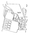
figure 3 shows a rear isometric view of the connector with a wire fixture in a partial closed position. - In respect of
figure 1 , an electrical connector of the type female socket module knows in the state of the art fromU.S. patent Nos. 5,947,761 incorporated by reference. The electrical connector includes adielectric housing 10, aterminal insert 12, acontact subassembly 14, and awire fixture 16. - The
housing 10 includes areceptacle portion 18 and aplatform portion 20. The receptacle portion has afront face 22, a rear face 24, and acavity 26 which opens into the receptacle portion though the front face. The cavity is configured as a receptacle for a mating modular plug. - On top of the
receptacle portion 18 is apivot block 28 which has a pair ofjournals 30 extending from opposite sides thereof. - The
platform portion 20 is disposed at a rear of thereceptacle portion 18. The platform portion includes abottom wall 32 andside walls 34 which haveopenings - The
terminal insert 12 includes acircuit board 38 and adielectric carrier 40 which holds a plurality ofterminals 42 in an array. Theterminals 42 havecontact sections 44 which are adjacent tofree ends 46, andopposite ends 48 which are electrically connected to circuit traces respectively imprinted on the printed circuit board. - The
contact subassembly 14 includes adielectric contact holder 50 which holds a plurality ofinsulation displacement contacts 52. Each of the contacts has a split beam which defines aslot 54 that can receive a wire. Edges of the split beam on opposite sides of the slot are configured to slice the insulation jacket on a wire which is installed in the slot and to electrically engage the wire conductive core of the respective line wire. - The
contacts 52 are arranged in the holder in laterally extending rows comprising afirst row 55 and asecond row 56 which are spaced-apart along a longitudinal axis of the connector. The rows extend parallel to each other. Thecontact holder 50 includes aseparator wall 58 between the tworows row - As best seen in
figures 2 and3 , thecontact subassembly 14 includes a horizontal U-shaped aperture opened through the lower wall of thesubassembly 14 and distanced from the furthest row of awall 51, which faces a rear face 24 of thereceptacle portion 18 and closes theterminals 42. The U-type aperture reveals part of the printed circuit board once the subassembly and theterminal insert 12 have been mounted in thedielectric housing 10. - Each of the
contacts 52 has asolder tail 60 which is received in a through-hole 39 in thecircuit board 38 and electrically terminated to a respective trace on the circuit board by soldering. In this way, thecontacts 52 are electrically connected to respective ones of theterminals 42 by traces on the circuit board. - The
circuit board 38 is configured to reside on thebottom wall 32 of thedielectric housing 10. Thecontact holder 50 haslatch tabs openings - As mentioned above, the printed
circuit board 38 is configured to receive anelectrical circuit 100 in a portion of the printed circuit board. Theelectrical circuit 100 is a type of polarising circuit includes a resistive 102 element type resistance and a switching 101 element type diode, transistor, etc.. The diode and the resistance are electrically connected in series and to respective tracks printed in the printedcircuit board 100 connects, in turn, toIDC connectors 52, andpredetermined terminals 42. - The
polarising 100 circuit is configured to be connected in parallel to the communication cable and made electrical checking in the same cable. Thepolarising 100 circuit is directly supplied through the own communication network. - The
wire fixture 16 is a dielectric member which is pivotally attached to thehousing 10 by a yoke having twobores 68 which receive thejournals 30 extending from thepivot block 28. Thewire fixture 16 is pivotable from a full open position to a closed position. - In the working or closed position of the
wire fixture 16, thepolarisation 100 circuit is protected from knocks and/or manipulation as it is covered completely by thewire fixture 16. - The
fixture 16 has alatch 98 which engages below thebottom wall 32 of the housing to retain the fixture in the closed working position. - The
wire fixture 16 comprises a wire insertion face 70 along a rear wall, atopside 72 and an underside 74. Thewire fixture 16 has passages 76 which are separated by walls 78. The passages 76 extend through the rear wall for a length downstream from the wire insertion face 70. The passages 76 are open along the underside 74 of the wire fixture for a significant portion of their length. Each of the passages has a cross-section which is dimensioned to receive a respective wires which are installed through the wire insertion face. - After being the wires positioned for insertion into the
slots 54 of theinsulation displacement contacts 52. Pivoting thewire fixture 16 to the closed position urges the wires into theslots 54 and into engagement with theinsulation displacement contacts 52. - During the pivotal movement of the
wire fixture 16, a significant force is required to push the wires into theslots 54. When the rotational movement has been completed, thelatch 98 of thewire fixture 16 has coupled beneath thebottom wall 32 of thehousing 10 retaining thefixture 16 in a closed position. - Therefore the electrical connector has been inserted.
Claims (12)
- An electrical connector for terminating a plurality of line wires of a communications cable, which comprises a dielectric housing (10); a terminal insert (12), a contact subassembly (14) and a wire fixture (16); characterised in that the terminal insert (12) includes a printed circuit board (38) is configured to receive a polarizing (100) circuit mounted thereon at a position rearward of the contact subassembly, the polarizing (100) circuit connected to a predetermined contact subset (52) included in the contact subassembly (14).
- Connector in accordance with claim 1; characterised in that the contact subassembly (14) includes contacts the type of insulation displacement contacts (52).
- Connector in accordance with claim 1; characterised in that the contact subassembly (14) is configured to cover partially the printed circuit board (38).
- Connector in accordance with claim 1; characterised in that the contact subassembly (14) is configured to fully cover the printed circuit board (38).
- Connector in accordance with claim 1; characterised in that the polarizing (100) circuit comprises a resistive (102) element and a switching (101) element electrically connected to make electrical checkout in the wires of communications cable electrically connected to the predetermined contacts subset (52).
- Connector in accordance with claim 5; characterised in that the resistive (102) element and the switching (101) element are electrically connected in series.
- Connector in accordance with claim 5; characterised in that the polarizing (100) circuit is connected in parallel to the communication cable.
- Connector in accordance with claim 5; characterised in that the switching element is a type of diode, transistor.
- Connector in accordance with claim 5; characterised in that the resistive element is a resistance.
- Connector in accordance with claim 3: characterised in that the wire fixture (16) in a closed or working position together to the dielectric housing (10) is configured to define a closed housing or partially closed housing too allow the remaining components of the electrical connector.
- Connector in accordance with claim 1; characterised in that the printed circuit board (38) is positioned below the contact subassembly (14).
- Connector in accordance with claim 11; characterised in that the contact subassembly (14) includes a horizontal U-shaped aperture opened through the lower wall and revealing part of the printed circuit board including the electrical circuit.
Priority Applications (4)
| Application Number | Priority Date | Filing Date | Title |
|---|---|---|---|
| EP11382071.6A EP2500992B1 (en) | 2011-03-16 | 2011-03-16 | Electrical conector |
| ES11382071.6T ES2529376T3 (en) | 2011-03-16 | 2011-03-16 | Electric connector |
| US13/419,257 US8613633B2 (en) | 2011-03-16 | 2012-03-13 | Electrical connector |
| CN201210080422.5A CN102868064B (en) | 2011-03-16 | 2012-03-16 | Electric connector |
Applications Claiming Priority (1)
| Application Number | Priority Date | Filing Date | Title |
|---|---|---|---|
| EP11382071.6A EP2500992B1 (en) | 2011-03-16 | 2011-03-16 | Electrical conector |
Publications (2)
| Publication Number | Publication Date |
|---|---|
| EP2500992A1 EP2500992A1 (en) | 2012-09-19 |
| EP2500992B1 true EP2500992B1 (en) | 2014-11-05 |
Family
ID=43866018
Family Applications (1)
| Application Number | Title | Priority Date | Filing Date |
|---|---|---|---|
| EP11382071.6A Not-in-force EP2500992B1 (en) | 2011-03-16 | 2011-03-16 | Electrical conector |
Country Status (4)
| Country | Link |
|---|---|
| US (1) | US8613633B2 (en) |
| EP (1) | EP2500992B1 (en) |
| CN (1) | CN102868064B (en) |
| ES (1) | ES2529376T3 (en) |
Families Citing this family (4)
| Publication number | Priority date | Publication date | Assignee | Title |
|---|---|---|---|---|
| US8764476B1 (en) * | 2012-12-06 | 2014-07-01 | Frank Ma | Transmission connector |
| US8992247B2 (en) | 2013-03-15 | 2015-03-31 | Ortronics, Inc. | Multi-surface contact plug assemblies, systems and methods |
| WO2017201177A1 (en) | 2016-05-20 | 2017-11-23 | Communications Systems, Inc. | Toolless communications jack |
| US10732358B2 (en) | 2016-11-09 | 2020-08-04 | Commscope Technologies Llc | Electrical-polarity switching hybrid interface |
Family Cites Families (19)
| Publication number | Priority date | Publication date | Assignee | Title |
|---|---|---|---|---|
| US6227911B1 (en) * | 1998-09-09 | 2001-05-08 | Amphenol Corporation | RJ contact/filter modules and multiport filter connector utilizing such modules |
| US5947761A (en) * | 1998-09-29 | 1999-09-07 | The Whitaker Corporation | Electrical connector with pivoting wire fixture |
| US6739912B2 (en) * | 2001-11-08 | 2004-05-25 | Hon Hai Precision Ind. Co., Ltd. | Modular jack assembly having improved positioning means |
| US20030211782A1 (en) * | 2002-05-07 | 2003-11-13 | Mr. Joseph Lorenzo De Guzman | Filtered RJ11 connector module with LED indicators and method of manufacturing |
| US7153163B2 (en) * | 2002-07-16 | 2006-12-26 | Tyco Electronics Corporation | Modular jack for ethernet applications |
| US6641440B1 (en) * | 2002-09-30 | 2003-11-04 | Hon Hai Precision Ind. Co., Ltd. | Electrical connector with power module |
| US6752664B2 (en) * | 2002-10-24 | 2004-06-22 | Hon Hai Precision Ind. Co., Ltd. | Modular jack having magnetic module with support and alignment mechanism |
| US6702618B1 (en) * | 2002-10-24 | 2004-03-09 | Hon Hai Precision Ind. Co., Ltd. | Modular jack having improved grounding plate |
| JP3800536B2 (en) * | 2002-12-06 | 2006-07-26 | Tdk株式会社 | Modular jack |
| TW200414634A (en) * | 2003-01-16 | 2004-08-01 | John Peng | Insulation displacement connector and manufacturing method thereof |
| EP2675022B1 (en) * | 2004-07-13 | 2014-09-03 | Panduit Corporation | Communications connector with flexible printed circuit board |
| US7443056B2 (en) * | 2006-06-29 | 2008-10-28 | Fisher Philip H | Junction device with logic and expansion capability |
| US7351083B2 (en) * | 2006-07-05 | 2008-04-01 | Hon Hai Precision Ind. Co., Ltd. | Electrical connector having terminating device |
| US7956618B2 (en) * | 2007-10-31 | 2011-06-07 | Sony Ericsson Mobile Communications Ab | Additional pins on a USB connector |
| TWM349123U (en) * | 2008-06-18 | 2009-01-11 | Surtec Ind Inc | Socket structure for communication cable |
| EP2345106B1 (en) * | 2008-10-07 | 2014-04-16 | Molex Incorporated | Termination cap for use in wired network management system |
| TW201021305A (en) * | 2008-11-28 | 2010-06-01 | Delta Electronics Inc | Connecter |
| US7611383B1 (en) * | 2008-12-22 | 2009-11-03 | Moxa, Inc. | RJ45 connector device having key structure for changing pin definitions |
| US7918684B2 (en) * | 2009-07-28 | 2011-04-05 | Lantek Electronics, Inc. | Shield-type communication socket |
-
2011
- 2011-03-16 EP EP11382071.6A patent/EP2500992B1/en not_active Not-in-force
- 2011-03-16 ES ES11382071.6T patent/ES2529376T3/en active Active
-
2012
- 2012-03-13 US US13/419,257 patent/US8613633B2/en not_active Expired - Fee Related
- 2012-03-16 CN CN201210080422.5A patent/CN102868064B/en not_active Expired - Fee Related
Also Published As
| Publication number | Publication date |
|---|---|
| ES2529376T3 (en) | 2015-02-19 |
| CN102868064A (en) | 2013-01-09 |
| CN102868064B (en) | 2016-05-11 |
| US8613633B2 (en) | 2013-12-24 |
| EP2500992A1 (en) | 2012-09-19 |
| US20120238153A1 (en) | 2012-09-20 |
Similar Documents
| Publication | Publication Date | Title |
|---|---|---|
| EP0969553B1 (en) | Terminating wire carrier module | |
| TWI356549B (en) | Interface adapter module | |
| EP0971444B1 (en) | Modular plug having a circuit board | |
| EP0519196B1 (en) | A terminal block for printed circuit boards | |
| US7553196B2 (en) | Telecommunications jack assembly | |
| US10950997B2 (en) | Plug module system | |
| TWI325664B (en) | Insulation displacement connector and equipment for telecommunications and data technology | |
| CN111509416A (en) | Plug-in electric connector | |
| US8403708B2 (en) | Terminating connector | |
| CN106019491A (en) | Hybrid socket connector and hybrid plug connector | |
| KR20090128329A (en) | Plug-in connector and method for connecting electrical conductors to a plug-in connector | |
| EP2939314B1 (en) | Interface adapter | |
| US8118601B2 (en) | Printed circuit board plug-type connector and connection module with printed circuit board plug-type connector | |
| EP2500992B1 (en) | Electrical conector | |
| WO2014150805A1 (en) | Multi-surface contact plug assemblies, systems and methods | |
| CA2291355C (en) | Printed circuit for modular plug | |
| EP1166400B1 (en) | Electrical connector | |
| US8257117B2 (en) | Electrical connector having a first group of terminals taller than that of a second group or located in a non-parallel plane | |
| CN201178176Y (en) | Electric connector | |
| US6375514B1 (en) | Wire connected modular jack connector assembly | |
| US6461200B1 (en) | Electrical connector assembly | |
| US20120039573A1 (en) | Connector | |
| EP1171933B1 (en) | Patch cord connector | |
| CN212991386U (en) | Self-short-circuit connector and corresponding connector assembly and plug-in terminal | |
| US10257919B1 (en) | Network socket device with compensation means |
Legal Events
| Date | Code | Title | Description |
|---|---|---|---|
| PUAI | Public reference made under article 153(3) epc to a published international application that has entered the european phase |
Free format text: ORIGINAL CODE: 0009012 |
|
| AK | Designated contracting states |
Kind code of ref document: A1 Designated state(s): AL AT BE BG CH CY CZ DE DK EE ES FI FR GB GR HR HU IE IS IT LI LT LU LV MC MK MT NL NO PL PT RO RS SE SI SK SM TR |
|
| AX | Request for extension of the european patent |
Extension state: BA ME |
|
| 17P | Request for examination filed |
Effective date: 20121221 |
|
| GRAP | Despatch of communication of intention to grant a patent |
Free format text: ORIGINAL CODE: EPIDOSNIGR1 |
|
| INTG | Intention to grant announced |
Effective date: 20140513 |
|
| GRAS | Grant fee paid |
Free format text: ORIGINAL CODE: EPIDOSNIGR3 |
|
| GRAA | (expected) grant |
Free format text: ORIGINAL CODE: 0009210 |
|
| AK | Designated contracting states |
Kind code of ref document: B1 Designated state(s): AL AT BE BG CH CY CZ DE DK EE ES FI FR GB GR HR HU IE IS IT LI LT LU LV MC MK MT NL NO PL PT RO RS SE SI SK SM TR |
|
| REG | Reference to a national code |
Ref country code: GB Ref legal event code: FG4D |
|
| REG | Reference to a national code |
Ref country code: CH Ref legal event code: EP |
|
| REG | Reference to a national code |
Ref country code: AT Ref legal event code: REF Ref document number: 695032 Country of ref document: AT Kind code of ref document: T Effective date: 20141115 |
|
| REG | Reference to a national code |
Ref country code: IE Ref legal event code: FG4D |
|
| RAP2 | Party data changed (patent owner data changed or rights of a patent transferred) |
Owner name: TYCO ELECTRONICS RAYCHEM BVBA Owner name: TE CONNECTIVITY AMP ESPANA S.L.U. |
|
| REG | Reference to a national code |
Ref country code: DE Ref legal event code: R096 Ref document number: 602011011081 Country of ref document: DE Effective date: 20141218 |
|
| REG | Reference to a national code |
Ref country code: GB Ref legal event code: 732E Free format text: REGISTERED BETWEEN 20141204 AND 20141211 |
|
| REG | Reference to a national code |
Ref country code: ES Ref legal event code: FG2A Ref document number: 2529376 Country of ref document: ES Kind code of ref document: T3 Effective date: 20150219 |
|
| REG | Reference to a national code |
Ref country code: NL Ref legal event code: VDEP Effective date: 20141105 |
|
| REG | Reference to a national code |
Ref country code: LT Ref legal event code: MG4D |
|
| PG25 | Lapsed in a contracting state [announced via postgrant information from national office to epo] |
Ref country code: IS Free format text: LAPSE BECAUSE OF FAILURE TO SUBMIT A TRANSLATION OF THE DESCRIPTION OR TO PAY THE FEE WITHIN THE PRESCRIBED TIME-LIMIT Effective date: 20150305 Ref country code: NL Free format text: LAPSE BECAUSE OF FAILURE TO SUBMIT A TRANSLATION OF THE DESCRIPTION OR TO PAY THE FEE WITHIN THE PRESCRIBED TIME-LIMIT Effective date: 20141105 Ref country code: LT Free format text: LAPSE BECAUSE OF FAILURE TO SUBMIT A TRANSLATION OF THE DESCRIPTION OR TO PAY THE FEE WITHIN THE PRESCRIBED TIME-LIMIT Effective date: 20141105 Ref country code: FI Free format text: LAPSE BECAUSE OF FAILURE TO SUBMIT A TRANSLATION OF THE DESCRIPTION OR TO PAY THE FEE WITHIN THE PRESCRIBED TIME-LIMIT Effective date: 20141105 Ref country code: PT Free format text: LAPSE BECAUSE OF FAILURE TO SUBMIT A TRANSLATION OF THE DESCRIPTION OR TO PAY THE FEE WITHIN THE PRESCRIBED TIME-LIMIT Effective date: 20150305 Ref country code: NO Free format text: LAPSE BECAUSE OF FAILURE TO SUBMIT A TRANSLATION OF THE DESCRIPTION OR TO PAY THE FEE WITHIN THE PRESCRIBED TIME-LIMIT Effective date: 20150205 |
|
| PG25 | Lapsed in a contracting state [announced via postgrant information from national office to epo] |
Ref country code: HR Free format text: LAPSE BECAUSE OF FAILURE TO SUBMIT A TRANSLATION OF THE DESCRIPTION OR TO PAY THE FEE WITHIN THE PRESCRIBED TIME-LIMIT Effective date: 20141105 Ref country code: CY Free format text: LAPSE BECAUSE OF FAILURE TO SUBMIT A TRANSLATION OF THE DESCRIPTION OR TO PAY THE FEE WITHIN THE PRESCRIBED TIME-LIMIT Effective date: 20141105 Ref country code: SE Free format text: LAPSE BECAUSE OF FAILURE TO SUBMIT A TRANSLATION OF THE DESCRIPTION OR TO PAY THE FEE WITHIN THE PRESCRIBED TIME-LIMIT Effective date: 20141105 Ref country code: LV Free format text: LAPSE BECAUSE OF FAILURE TO SUBMIT A TRANSLATION OF THE DESCRIPTION OR TO PAY THE FEE WITHIN THE PRESCRIBED TIME-LIMIT Effective date: 20141105 Ref country code: RS Free format text: LAPSE BECAUSE OF FAILURE TO SUBMIT A TRANSLATION OF THE DESCRIPTION OR TO PAY THE FEE WITHIN THE PRESCRIBED TIME-LIMIT Effective date: 20141105 Ref country code: PL Free format text: LAPSE BECAUSE OF FAILURE TO SUBMIT A TRANSLATION OF THE DESCRIPTION OR TO PAY THE FEE WITHIN THE PRESCRIBED TIME-LIMIT Effective date: 20141105 Ref country code: GR Free format text: LAPSE BECAUSE OF FAILURE TO SUBMIT A TRANSLATION OF THE DESCRIPTION OR TO PAY THE FEE WITHIN THE PRESCRIBED TIME-LIMIT Effective date: 20150206 |
|
| PG25 | Lapsed in a contracting state [announced via postgrant information from national office to epo] |
Ref country code: DK Free format text: LAPSE BECAUSE OF FAILURE TO SUBMIT A TRANSLATION OF THE DESCRIPTION OR TO PAY THE FEE WITHIN THE PRESCRIBED TIME-LIMIT Effective date: 20141105 Ref country code: EE Free format text: LAPSE BECAUSE OF FAILURE TO SUBMIT A TRANSLATION OF THE DESCRIPTION OR TO PAY THE FEE WITHIN THE PRESCRIBED TIME-LIMIT Effective date: 20141105 Ref country code: SK Free format text: LAPSE BECAUSE OF FAILURE TO SUBMIT A TRANSLATION OF THE DESCRIPTION OR TO PAY THE FEE WITHIN THE PRESCRIBED TIME-LIMIT Effective date: 20141105 Ref country code: CZ Free format text: LAPSE BECAUSE OF FAILURE TO SUBMIT A TRANSLATION OF THE DESCRIPTION OR TO PAY THE FEE WITHIN THE PRESCRIBED TIME-LIMIT Effective date: 20141105 |
|
| REG | Reference to a national code |
Ref country code: DE Ref legal event code: R097 Ref document number: 602011011081 Country of ref document: DE |
|
| PLBE | No opposition filed within time limit |
Free format text: ORIGINAL CODE: 0009261 |
|
| STAA | Information on the status of an ep patent application or granted ep patent |
Free format text: STATUS: NO OPPOSITION FILED WITHIN TIME LIMIT |
|
| 26N | No opposition filed |
Effective date: 20150806 |
|
| PG25 | Lapsed in a contracting state [announced via postgrant information from national office to epo] |
Ref country code: LU Free format text: LAPSE BECAUSE OF FAILURE TO SUBMIT A TRANSLATION OF THE DESCRIPTION OR TO PAY THE FEE WITHIN THE PRESCRIBED TIME-LIMIT Effective date: 20150316 Ref country code: MC Free format text: LAPSE BECAUSE OF FAILURE TO SUBMIT A TRANSLATION OF THE DESCRIPTION OR TO PAY THE FEE WITHIN THE PRESCRIBED TIME-LIMIT Effective date: 20141105 |
|
| REG | Reference to a national code |
Ref country code: CH Ref legal event code: PL |
|
| REG | Reference to a national code |
Ref country code: IE Ref legal event code: MM4A |
|
| PG25 | Lapsed in a contracting state [announced via postgrant information from national office to epo] |
Ref country code: IE Free format text: LAPSE BECAUSE OF NON-PAYMENT OF DUE FEES Effective date: 20150316 Ref country code: CH Free format text: LAPSE BECAUSE OF NON-PAYMENT OF DUE FEES Effective date: 20150331 Ref country code: LI Free format text: LAPSE BECAUSE OF NON-PAYMENT OF DUE FEES Effective date: 20150331 |
|
| PG25 | Lapsed in a contracting state [announced via postgrant information from national office to epo] |
Ref country code: SI Free format text: LAPSE BECAUSE OF FAILURE TO SUBMIT A TRANSLATION OF THE DESCRIPTION OR TO PAY THE FEE WITHIN THE PRESCRIBED TIME-LIMIT Effective date: 20141105 |
|
| REG | Reference to a national code |
Ref country code: FR Ref legal event code: PLFP Year of fee payment: 6 |
|
| PG25 | Lapsed in a contracting state [announced via postgrant information from national office to epo] |
Ref country code: RO Free format text: LAPSE BECAUSE OF FAILURE TO SUBMIT A TRANSLATION OF THE DESCRIPTION OR TO PAY THE FEE WITHIN THE PRESCRIBED TIME-LIMIT Effective date: 20141105 |
|
| PG25 | Lapsed in a contracting state [announced via postgrant information from national office to epo] |
Ref country code: MT Free format text: LAPSE BECAUSE OF FAILURE TO SUBMIT A TRANSLATION OF THE DESCRIPTION OR TO PAY THE FEE WITHIN THE PRESCRIBED TIME-LIMIT Effective date: 20141105 |
|
| REG | Reference to a national code |
Ref country code: FR Ref legal event code: PLFP Year of fee payment: 7 |
|
| PG25 | Lapsed in a contracting state [announced via postgrant information from national office to epo] |
Ref country code: BG Free format text: LAPSE BECAUSE OF FAILURE TO SUBMIT A TRANSLATION OF THE DESCRIPTION OR TO PAY THE FEE WITHIN THE PRESCRIBED TIME-LIMIT Effective date: 20141105 Ref country code: SM Free format text: LAPSE BECAUSE OF FAILURE TO SUBMIT A TRANSLATION OF THE DESCRIPTION OR TO PAY THE FEE WITHIN THE PRESCRIBED TIME-LIMIT Effective date: 20141105 Ref country code: HU Free format text: LAPSE BECAUSE OF FAILURE TO SUBMIT A TRANSLATION OF THE DESCRIPTION OR TO PAY THE FEE WITHIN THE PRESCRIBED TIME-LIMIT; INVALID AB INITIO Effective date: 20110316 |
|
| PG25 | Lapsed in a contracting state [announced via postgrant information from national office to epo] |
Ref country code: TR Free format text: LAPSE BECAUSE OF FAILURE TO SUBMIT A TRANSLATION OF THE DESCRIPTION OR TO PAY THE FEE WITHIN THE PRESCRIBED TIME-LIMIT Effective date: 20141105 |
|
| PG25 | Lapsed in a contracting state [announced via postgrant information from national office to epo] |
Ref country code: BE Free format text: LAPSE BECAUSE OF FAILURE TO SUBMIT A TRANSLATION OF THE DESCRIPTION OR TO PAY THE FEE WITHIN THE PRESCRIBED TIME-LIMIT Effective date: 20141105 |
|
| REG | Reference to a national code |
Ref country code: FR Ref legal event code: PLFP Year of fee payment: 8 |
|
| PGFP | Annual fee paid to national office [announced via postgrant information from national office to epo] |
Ref country code: GB Payment date: 20180327 Year of fee payment: 8 |
|
| PGFP | Annual fee paid to national office [announced via postgrant information from national office to epo] |
Ref country code: IT Payment date: 20180322 Year of fee payment: 8 Ref country code: AT Payment date: 20180305 Year of fee payment: 8 Ref country code: FR Payment date: 20180326 Year of fee payment: 8 |
|
| REG | Reference to a national code |
Ref country code: AT Ref legal event code: UEP Ref document number: 695032 Country of ref document: AT Kind code of ref document: T Effective date: 20141105 |
|
| PG25 | Lapsed in a contracting state [announced via postgrant information from national office to epo] |
Ref country code: MK Free format text: LAPSE BECAUSE OF FAILURE TO SUBMIT A TRANSLATION OF THE DESCRIPTION OR TO PAY THE FEE WITHIN THE PRESCRIBED TIME-LIMIT Effective date: 20141105 |
|
| PGFP | Annual fee paid to national office [announced via postgrant information from national office to epo] |
Ref country code: DE Payment date: 20180328 Year of fee payment: 8 Ref country code: ES Payment date: 20180402 Year of fee payment: 8 |
|
| PG25 | Lapsed in a contracting state [announced via postgrant information from national office to epo] |
Ref country code: AL Free format text: LAPSE BECAUSE OF FAILURE TO SUBMIT A TRANSLATION OF THE DESCRIPTION OR TO PAY THE FEE WITHIN THE PRESCRIBED TIME-LIMIT Effective date: 20141105 |
|
| REG | Reference to a national code |
Ref country code: DE Ref legal event code: R119 Ref document number: 602011011081 Country of ref document: DE |
|
| REG | Reference to a national code |
Ref country code: AT Ref legal event code: MM01 Ref document number: 695032 Country of ref document: AT Kind code of ref document: T Effective date: 20190316 |
|
| GBPC | Gb: european patent ceased through non-payment of renewal fee |
Effective date: 20190316 |
|
| PG25 | Lapsed in a contracting state [announced via postgrant information from national office to epo] |
Ref country code: DE Free format text: LAPSE BECAUSE OF NON-PAYMENT OF DUE FEES Effective date: 20191001 Ref country code: AT Free format text: LAPSE BECAUSE OF NON-PAYMENT OF DUE FEES Effective date: 20190316 Ref country code: GB Free format text: LAPSE BECAUSE OF NON-PAYMENT OF DUE FEES Effective date: 20190316 |
|
| PG25 | Lapsed in a contracting state [announced via postgrant information from national office to epo] |
Ref country code: FR Free format text: LAPSE BECAUSE OF NON-PAYMENT OF DUE FEES Effective date: 20190331 Ref country code: IT Free format text: LAPSE BECAUSE OF NON-PAYMENT OF DUE FEES Effective date: 20190316 |
|
| REG | Reference to a national code |
Ref country code: ES Ref legal event code: FD2A Effective date: 20200727 |
|
| PG25 | Lapsed in a contracting state [announced via postgrant information from national office to epo] |
Ref country code: ES Free format text: LAPSE BECAUSE OF NON-PAYMENT OF DUE FEES Effective date: 20190317 |