EP2415131B1 - Light source, and optical coherence tomography module - Google Patents
Light source, and optical coherence tomography module Download PDFInfo
- Publication number
- EP2415131B1 EP2415131B1 EP10701611.5A EP10701611A EP2415131B1 EP 2415131 B1 EP2415131 B1 EP 2415131B1 EP 10701611 A EP10701611 A EP 10701611A EP 2415131 B1 EP2415131 B1 EP 2415131B1
- Authority
- EP
- European Patent Office
- Prior art keywords
- optical
- light
- resonator
- light source
- optical module
- Prior art date
- Legal status (The legal status is an assumption and is not a legal conclusion. Google has not performed a legal analysis and makes no representation as to the accuracy of the status listed.)
- Active
Links
- 0 CC1C2(C)C3=CCC(C)(CCCC(CCC4)CC4=*)CC3[C@@]1C2 Chemical compound CC1C2(C)C3=CCC(C)(CCCC(CCC4)CC4=*)CC3[C@@]1C2 0.000 description 1
Images


Classifications
-
- H—ELECTRICITY
- H01—ELECTRIC ELEMENTS
- H01S—DEVICES USING THE PROCESS OF LIGHT AMPLIFICATION BY STIMULATED EMISSION OF RADIATION [LASER] TO AMPLIFY OR GENERATE LIGHT; DEVICES USING STIMULATED EMISSION OF ELECTROMAGNETIC RADIATION IN WAVE RANGES OTHER THAN OPTICAL
- H01S5/00—Semiconductor lasers
- H01S5/06—Arrangements for controlling the laser output parameters, e.g. by operating on the active medium
-
- G—PHYSICS
- G01—MEASURING; TESTING
- G01N—INVESTIGATING OR ANALYSING MATERIALS BY DETERMINING THEIR CHEMICAL OR PHYSICAL PROPERTIES
- G01N21/00—Investigating or analysing materials by the use of optical means, i.e. using sub-millimetre waves, infrared, visible or ultraviolet light
- G01N21/17—Systems in which incident light is modified in accordance with the properties of the material investigated
- G01N21/47—Scattering, i.e. diffuse reflection
- G01N21/4795—Scattering, i.e. diffuse reflection spatially resolved investigating of object in scattering medium
-
- G—PHYSICS
- G01—MEASURING; TESTING
- G01B—MEASURING LENGTH, THICKNESS OR SIMILAR LINEAR DIMENSIONS; MEASURING ANGLES; MEASURING AREAS; MEASURING IRREGULARITIES OF SURFACES OR CONTOURS
- G01B9/00—Measuring instruments characterised by the use of optical techniques
- G01B9/02—Interferometers
- G01B9/02001—Interferometers characterised by controlling or generating intrinsic radiation properties
- G01B9/02002—Interferometers characterised by controlling or generating intrinsic radiation properties using two or more frequencies
- G01B9/02004—Interferometers characterised by controlling or generating intrinsic radiation properties using two or more frequencies using frequency scans
-
- G—PHYSICS
- G01—MEASURING; TESTING
- G01B—MEASURING LENGTH, THICKNESS OR SIMILAR LINEAR DIMENSIONS; MEASURING ANGLES; MEASURING AREAS; MEASURING IRREGULARITIES OF SURFACES OR CONTOURS
- G01B9/00—Measuring instruments characterised by the use of optical techniques
- G01B9/02—Interferometers
- G01B9/0209—Low-coherence interferometers
- G01B9/02091—Tomographic interferometers, e.g. based on optical coherence
-
- H—ELECTRICITY
- H01—ELECTRIC ELEMENTS
- H01S—DEVICES USING THE PROCESS OF LIGHT AMPLIFICATION BY STIMULATED EMISSION OF RADIATION [LASER] TO AMPLIFY OR GENERATE LIGHT; DEVICES USING STIMULATED EMISSION OF ELECTROMAGNETIC RADIATION IN WAVE RANGES OTHER THAN OPTICAL
- H01S5/00—Semiconductor lasers
- H01S5/10—Construction or shape of the optical resonator, e.g. extended or external cavity, coupled cavities, bent-guide, varying width, thickness or composition of the active region
- H01S5/14—External cavity lasers
- H01S5/141—External cavity lasers using a wavelength selective device, e.g. a grating or etalon
-
- H—ELECTRICITY
- H01—ELECTRIC ELEMENTS
- H01S—DEVICES USING THE PROCESS OF LIGHT AMPLIFICATION BY STIMULATED EMISSION OF RADIATION [LASER] TO AMPLIFY OR GENERATE LIGHT; DEVICES USING STIMULATED EMISSION OF ELECTROMAGNETIC RADIATION IN WAVE RANGES OTHER THAN OPTICAL
- H01S3/00—Lasers, i.e. devices using stimulated emission of electromagnetic radiation in the infrared, visible or ultraviolet wave range
- H01S3/05—Construction or shape of optical resonators; Accommodation of active medium therein; Shape of active medium
- H01S3/08—Construction or shape of optical resonators or components thereof
- H01S3/081—Construction or shape of optical resonators or components thereof comprising three or more reflectors
- H01S3/0813—Configuration of resonator
-
- H—ELECTRICITY
- H01—ELECTRIC ELEMENTS
- H01S—DEVICES USING THE PROCESS OF LIGHT AMPLIFICATION BY STIMULATED EMISSION OF RADIATION [LASER] TO AMPLIFY OR GENERATE LIGHT; DEVICES USING STIMULATED EMISSION OF ELECTROMAGNETIC RADIATION IN WAVE RANGES OTHER THAN OPTICAL
- H01S5/00—Semiconductor lasers
- H01S5/02—Structural details or components not essential to laser action
- H01S5/022—Mountings; Housings
- H01S5/02208—Mountings; Housings characterised by the shape of the housings
- H01S5/02216—Butterfly-type, i.e. with electrode pins extending horizontally from the housings
-
- H—ELECTRICITY
- H01—ELECTRIC ELEMENTS
- H01S—DEVICES USING THE PROCESS OF LIGHT AMPLIFICATION BY STIMULATED EMISSION OF RADIATION [LASER] TO AMPLIFY OR GENERATE LIGHT; DEVICES USING STIMULATED EMISSION OF ELECTROMAGNETIC RADIATION IN WAVE RANGES OTHER THAN OPTICAL
- H01S5/00—Semiconductor lasers
- H01S5/02—Structural details or components not essential to laser action
- H01S5/022—Mountings; Housings
- H01S5/0225—Out-coupling of light
- H01S5/02251—Out-coupling of light using optical fibres
-
- H—ELECTRICITY
- H01—ELECTRIC ELEMENTS
- H01S—DEVICES USING THE PROCESS OF LIGHT AMPLIFICATION BY STIMULATED EMISSION OF RADIATION [LASER] TO AMPLIFY OR GENERATE LIGHT; DEVICES USING STIMULATED EMISSION OF ELECTROMAGNETIC RADIATION IN WAVE RANGES OTHER THAN OPTICAL
- H01S5/00—Semiconductor lasers
- H01S5/02—Structural details or components not essential to laser action
- H01S5/022—Mountings; Housings
- H01S5/023—Mount members, e.g. sub-mount members
- H01S5/02325—Mechanically integrated components on mount members or optical micro-benches
-
- H—ELECTRICITY
- H01—ELECTRIC ELEMENTS
- H01S—DEVICES USING THE PROCESS OF LIGHT AMPLIFICATION BY STIMULATED EMISSION OF RADIATION [LASER] TO AMPLIFY OR GENERATE LIGHT; DEVICES USING STIMULATED EMISSION OF ELECTROMAGNETIC RADIATION IN WAVE RANGES OTHER THAN OPTICAL
- H01S5/00—Semiconductor lasers
- H01S5/02—Structural details or components not essential to laser action
- H01S5/024—Arrangements for thermal management
- H01S5/02407—Active cooling, e.g. the laser temperature is controlled by a thermo-electric cooler or water cooling
- H01S5/02415—Active cooling, e.g. the laser temperature is controlled by a thermo-electric cooler or water cooling by using a thermo-electric cooler [TEC], e.g. Peltier element
-
- H—ELECTRICITY
- H01—ELECTRIC ELEMENTS
- H01S—DEVICES USING THE PROCESS OF LIGHT AMPLIFICATION BY STIMULATED EMISSION OF RADIATION [LASER] TO AMPLIFY OR GENERATE LIGHT; DEVICES USING STIMULATED EMISSION OF ELECTROMAGNETIC RADIATION IN WAVE RANGES OTHER THAN OPTICAL
- H01S5/00—Semiconductor lasers
- H01S5/02—Structural details or components not essential to laser action
- H01S5/024—Arrangements for thermal management
- H01S5/02438—Characterized by cooling of elements other than the laser chip, e.g. an optical element being part of an external cavity or a collimating lens
-
- H—ELECTRICITY
- H01—ELECTRIC ELEMENTS
- H01S—DEVICES USING THE PROCESS OF LIGHT AMPLIFICATION BY STIMULATED EMISSION OF RADIATION [LASER] TO AMPLIFY OR GENERATE LIGHT; DEVICES USING STIMULATED EMISSION OF ELECTROMAGNETIC RADIATION IN WAVE RANGES OTHER THAN OPTICAL
- H01S5/00—Semiconductor lasers
- H01S5/06—Arrangements for controlling the laser output parameters, e.g. by operating on the active medium
- H01S5/068—Stabilisation of laser output parameters
- H01S5/0683—Stabilisation of laser output parameters by monitoring the optical output parameters
-
- H—ELECTRICITY
- H01—ELECTRIC ELEMENTS
- H01S—DEVICES USING THE PROCESS OF LIGHT AMPLIFICATION BY STIMULATED EMISSION OF RADIATION [LASER] TO AMPLIFY OR GENERATE LIGHT; DEVICES USING STIMULATED EMISSION OF ELECTROMAGNETIC RADIATION IN WAVE RANGES OTHER THAN OPTICAL
- H01S5/00—Semiconductor lasers
- H01S5/10—Construction or shape of the optical resonator, e.g. extended or external cavity, coupled cavities, bent-guide, varying width, thickness or composition of the active region
- H01S5/14—External cavity lasers
- H01S5/141—External cavity lasers using a wavelength selective device, e.g. a grating or etalon
- H01S5/143—Littman-Metcalf configuration, e.g. laser - grating - mirror
Definitions
- the invention is in the field of light sources, i.e. of sources of electromagnetic radiation in the infrared, visible, and ultraviolet part of the electromagnetic radiation spectrum. More concretely, the invention concerns a swept light source, such as for use in optical coherence tomography, and to a corresponding module.
- OCT Optical Coherence Tomography
- OCT is the optical analog of ultrasound but takes advantage of the shorter wavelengths of light to achieve higher resolution images. Potentially the wavelength ranges of interest lie within the visible to near infrared regions of the spectrum from 400-2000nm.
- OCT systems comprise (1) a broadband light source, (2) an arrangement of optical components for directing the emitted radiation to a sample and to a reference mirror and (3) an optical arrangement for measurement of interference of light reflected from the sample and light reflected from the reference mirror.
- the broadband source is a superluminescent light emitting diode (SLED) which emits light in a broad spectrum of wavelengths (40-200nm bandwidth), and the sub-surface imaging depth is controlled by scanning the position of the reference mirror.
- Constructive interference only occurs when the path-lengths between the reference mirror and sample reflectors are equal within the coherence length of the light source.
- Fourier or Frequency domain OCT (FD-OCT) makes use of spectral frequency information, for example by decoding the interference using a dispersive element and a CCD detector array or Spectrometer (Spectral Domain OCT or SD-OCT).
- Another FD-OCT technique requiring a simpler detection system, uses spectral encoding in time by spectrally scanning a narrow bandwidth light source (Swept Source OCT or SS-OCT).
- SS-OCT a tunable laser is used as the light source.
- SS-OCT has been demonstrated to have major signal to noise advantages over TD-OCT (see Choma et al, Optics Express, vol. 11, 2003 pp. 2183-2189 ).
- swept source OCT systems require tunable light sources that can be swept across a wavelength range at high frequencies of 20-400kHz. Since the imaging depth required for the interferometers of these systems is related to the coherence length of the light source, this also sets the requirements for the linewidth and line spacing of the light source.
- Simpler and more versatile designs are based on external cavity lasers where the filtering and wavelength sweep functions are performed by a grating and a rotating or scanning mirror ( US 6,111,645 , US 5,907,423 , US 2007/0276269 , US 2007/0239035 , US 2007/0064239 , US 2008/0043244 , US 2004/0213306 ).
- These designs are versatile, since they can relatively easily be adapted for other wavelength ranges.
- Swept-source OCT applications require the swept source to have a coherence length that is above a certain minimum value and below a certain maximum value.
- an external cavity tuneable laser which comprises a Fabry Perot etalon placed in the cavity which is structured and configured to define a plurality of equally spaced transmission peaks. Furthermore, an optical control ssytem is provided which comprises a first and a second photodetector placed on a beam splitter and a filter having a wavelength-dependent transmission placed between the beam splitter and the second photodetector, for determining the lasing wavelength. From US 2006/0215713 A1 , an external cavity laser is known which has a mirror-based resonant tunable filter, such as a Fabry Perot tunable filter.
- An advantage of the approach according to a first aspect of the invention is that the light source components - and possibly elements of further devices such as intensity detector(s), beam splitter/combiner, a wavemeter and/or even a reference arm of an OCT set-up - are integrated in a common package.
- the devices integrated in the package preferably include the moving parts such as a MEMS grating or an MEMS mirror.
- the devices of the package have a common thermoelectric cooler that is in contact with a mount on which a plurality of the components within the module casing are arranged. This brings about further advantages in terms of stability and reproducibility as well as being advantageous in terms of manufacturing complexity.
- the invention proposes to provide a swept light source with a wavelength selector (that may comprise a movable MEMS mirror and a grating or a Fabry-Perot filter tuning element (for example a Fabry-Perot MEMS device), or a rotating scanning mirror and a grating, etc.) and proposes, where it refers to light sources of a first type, multimode operation.
- Multimode operation makes possible that the coherence length can be controlled not to exceed a certain maximum acceptable value.
- Mode-hopping means that the laser will turn off lasing operation for a short period of time and then turn on lasing operation again once the tunable filter coincides with the next lasing mode.
- the turn-on process of a laser can be a relatively slow process (relative to the fast sweep rates that are required for SS-OCT applications) because stimulated laser emission has to build up from spontaneous emission and amplified spontaneous emission and therefore stable laser operation with low noise and good signal-to-noise ratio will require several round-trips in the laser cavity.
- a multimode laser cavity is advantageous for fast wavelength tuning because the laser cavity can be kept lasing during the wavelength sweep.
- the laser cavity should not be too long (unless special techniques like Fourier-domain mode-locking (FDML) are used) because the associated long round-trip times would prohibit fast wavelength tuning again.
- FDML Fourier-domain mode-locking
- the fraction of the path length taken up in the retarding device is to be just high enough to enable the integration of an optical cavity within an optical package.
- the optical retarding device in which the light traces within the device are not necessarily parallel.
- a "pass" is a path portion inside the redarding device in between two subsequent reflections.
- the optical package is for example closed - and possibly sealed - against the outside so that the components on the base are at most accessible by the electrical feedthroughs and/or the optical feedthroughs.
- the retarding device enables miniaturisation of the tunable external cavity arrangement so that it can be assembled into standard optical modules such as, for example, those known in the art as butterfly packages.
- the relatively simple optical arrangement is easily adaptable to operate at all the wavelength ranges of interest for SS-OCT by employing suitable gain blocks (or, as the case may be, resonator geometries of a free-space resonator) and optical coatings on components.
- the dimensions of the overall package are compact, with a two-dimensionsal extension (in the plane of the mount) of preferably not greater than 22 mm*60 mm, in a preferred embodiment not greater than 13 mmx30 mm.
- a two-dimensionsal extension is not greater than 22 mm*60 mm*20 mm, preferably not greater than 20 mm*40 mm*20 mm, especially not greater than 15 mm*35 mm*10 mm or not greater than 13 mm*30 mm*10 mm.
- the retarding device comprises a plurality of reflective surfaces for reflecting back and forth light portions propagating in the block of material.
- the retarding device may be a block of material, for example of Silica or LiNbO 3 or any other suitable material transparent for the light wavelengths concerned.
- the block may have two opposing surfaces that may be essentially parallel and that may be at least partially coated to be reflective. Suitable coatings may include metal coatings , dielectric coatings or other reflective layers.
- the light path within the retarding device may be defined by at least one of:
- the retarding device may comprise a circulating optical waveguide design.
- the body is designed and arranged so that the light path in the resonator is perpendicular to the respective end facet at non-reflective entrance and exit end facets (the distinction between the entrance and the exit is somewhat arbitrary: in the resonator the light will enter and exit both, through the entrance and the exit facets) and is non-perpendicular to the facets at least partially provided with a reflective coating.
- the body of transparent material may for example be made of glass (a suitable material especially for embodiments where the light for being internally reflected impinges on a low angle), silica, a polymer, a semiconductor compound, etc.
- the retarding device body has a generally rhomboid shape with a first facet and a second facet not parallel to the first facet.
- the retarding device is arranged so that the angle of incidence on the first facet is perpendicular.
- the light path in the retarding device is defined by geometrical optics.
- the second facet or the first facet comprises an angled portion so that the when exiting the light path is perpendicular to the surface through which it exits.
- the retarding device may comprise an optical waveguide design with waveguides defined at different vertical planes to enable longer beam path lengths in the retarding device.
- Such an optical waveguide design also facilitates coupling to optical components having optical axes at different levels.
- the retarding device may include one or more optical directional couplers. Such a directional coupler may be used for splitting the light in the retarding device between a resonator path and a monitoring path, between a sample output and a reference output, and/or also between an input and an imaging output.
- the wavelength selector may comprise a scanning Micro-Opto-Electro-Mechanical Systems (MOEMS) mirror (sometimes also termed MEMS mirror) cooperating with a wavelength selective element, such as a grating.
- MOEMS Micro-Opto-Electro-Mechanical Systems
- the MOEMS mirror and grating component are arranged to provide the tunable feature of the external cavity laser.
- the grating acts as a filter to select a narrow range of wavelengths for the cavity.
- the MOEMS mirror is scanned to vary the incident angle of light onto the grating such that the center wavelength of the narrow range of wavelengths can be varied.
- the grating could be integrated on the surface of the MOEMS scanning device.
- MOEMS devices mirrors or, as an alternative for example also a MOEMS prism could be used
- MOEMS prisms feature the advantage of having dimensions suitable for integration on the common base and in the optoelectronic package, without any negative influence on the overall size.
- the integrated swept wavelength light source also comprises a monitor, such as a monitoring photodiode, also arranged on the common base.
- the monitor is arranged so that a representative portion of the light circulating in the resonator is coupled out of the resonator and directed onto the monitor.
- the monitor comprises an electronic monitor output that is contactable by way of an electrical feedthrough from outside of the module so as to provide the possibility of an electronic control of the light source.
- the gain device has reflective end facet that is used as resonator end mirror.
- the partially transparent laser outcoupling mirror may be replaced by the (partially) reflective end facet of the gain device.
- Semiconductor gain devices with a reflective end facet correspond to reflective semiconductor optical amplifiers (R-SOAs).
- R-SOAs reflective semiconductor optical amplifiers
- the light has to be coupled into the gain device only once in every roundtrip in the resonator instead of twice. This may bring about a substantial reduction of the cavity loss and may therefore improve the swept-wavelength light source in power, tuning speed, tuning range, signa-to-noise ratio and/or other optical parameters.
- embodiments of the second aspect may be implemented according to one of the following designs:
- side refers to an optical beam path in the resonator.
- the gain block used may be a reflective semiconductor optical amplifier (that in itself may be a resonator).
- Optical radiation propagates along a path which extends from the partially-reflective (for example 3-80%) facet of the R-SOA through the retarding device and is, for example, reflected by the MEMs mirror onto the grating.
- the optical path length between the R-SOA and the grating defines the length of the resonator (cavity) and the coherence properties of the swept source.
- the external cavity laser light is coupled to an optical fiber at the partially reflective semiconductor optical amplifier.
- the gain block used may be a (non-reflective - for example ⁇ 0.5%) semiconductor optical amplifier (SOA), a separate outcoupling mirror being provided.
- SOA semiconductor optical amplifier
- Embodiments with the R-SOA are, however, more compact.
- the retarding device provides an additional interferometer with outputs that are coupled to an optical fiber or to a plurality of optical fibers.
- the light source may further comprise an electronic controller to regulate and adjust its performance.
- This may comprise a controlling device, for example including controlling electronic components and/or controlling software and/or firmware running on generic hardware, such as on a PC, a microprocessor, a microcontroller, or an FPGA.
- the controller is connected or connectable to the components on the base by electrical contact means, such as the electrical feedthroughs.
- the invention also concerns an optical coherence tomography apparatus, the apparatus comprising:
- the optical coherence tomography apparatus of the above-defined kind comprises a light source according to such an embodiment
- the portion of the interferometer (being formed by the directional coupler) is integrated in the light source, and so is optionally the detector.
- the optics unit may have to be merely provided with the integrated light source and detector module.
- the invention further also refers to an optical coherence tomography module for an optical coherence tomography apparatus, the module comprising:
- the module may, in addition to the light source, comprise:
- the module is the integrated light source.
- the module may, in addition to the packaged light source, comprise a separate, but potentially fixedly attached interferometer and detector.
- the module may further comprise, externally to the module casing, an electronics unit that includes an analyzer and/or evaluator for evaluating data produced by the sensor arrangement.
- the light source in accordance with any aspect of the invention may further incorporate measures for ensuring that the sweeping is linear or approximately linear.
- a resonator if the moving part(s) is/are just driven by an electrical signal linear in time, or of a resonant MEMS structure, for example driven by a clock-like signal to oscillate sinusoidally, is used, often a non-linear frequency dependency of the output radiation will result.
- the measures incorporated may include one or more of the following:
- the filter device is chosen so that in the light source wavelength range, in which the light source output wavelength sweeps, the filter characteristics has a pronounced wavelength dependence.
- the filter transmission characteristic is a strictly monotonous function of the wavelength.
- the difference between the transmission at the lowest wavelength of the wavelength range, and the transmission of the highest wavelength of the wavelength range is then preferably as high as possible.
- the filter may be a high-pass filter or a low-pass filter.
- the filter is a bandpass filter, the passband of which is offset relative to the wavelength range, so that the wavelength range is in a sloped portion of the filter transmission characteristics.
- bandpass filters available that have, within the wavelength range used for example for swept-source OCT, a steep characteristic.
- an optical filter with a periodic transmissive or reflective response in the frequency domain (k-space) for example a Mach-Zehnder interferometer or a Fabry-Perot filter
- k-space for example a Mach-Zehnder interferometer or a Fabry-Perot filter
- This optical k-clock signal is detected by a photodetector and converted into an electrical k-clock signal that is then synchronized with other clock signals of the SS-OCT system responsible, for example, for sampling the received OCT signal from the interferometer.
- the proposed wavemeter according to the third aspect of the invention is simple, robust, has not moving parts, and the output signals are easy to analyze.
- the signal from the wavemeter is independent of the optical output power of the swept laser and hence a true meausure of the wavelength or frequency.
- the electronics unit of the module thus further comprises a clock, the clock being operable to trigger a sampling of the first and second wavemeter detector signals.
- the clock may further be operable to trigger a sampling of a wanted intensity signal.
- Embodiments of the invention go in an other direction by proposing to use it such a filter as a component of a wavemeter that can be sampled synchronously with the signal.
- the resonator design ins based on the so-called Littrow configuration, where the diffraction grating acts as a resonator mirror.
- the invention pertaining to all embodiments, is not restricted to such configuration.
- the skilled person will know other resonator configurations of tunable resonators for externa-cavity diode lasers.
- An other known configuration is the so-called Littman-Metcalf configuration where a separate mirror (that may be the movable device), onto which diffracted radiation is directed, is used as an end mirror.
- the skilled person will know ways to re-arrange resonator components in a manner that the grating is not a resonator end mirror.
- the lens 107 is used to image the light onto the MEMS mirror such that the image size changes between lens 107, MEMS mirror 103 and diffraction grating 104.
- any suitable arrangement of imaging and/or collimating means that may, in addition or as alternative to lenses may include appropriately shaped reflectors
- radiation directing means may be used.
- optical waveguide tapers may be provided by the retarding device to couple light directly to the gain block.
- the MEMS mirror used in this embodiment preferably scans at frequencies of 20-400kHz and is driven by either a resonant or linear ramp waveform.
- the monitor diode is arranged in a position where it is hit by light portions different from the light portions directed back into the resonator by the grating; for example when the -1 st diffraction order is directed back into the resonator, the 1 st diffraction order or the 0 th diffraction order may be directed onto the monitor diode 105.
- Light from the laser is coupled by a coupling lens 108 into an optical fiber 109.
- Figure 2 is a view of the assembly of the external tunable laser into a module.
- the R-SOA 102 is mounted on a first submount 111 and the fiber 109 is mounted on a second submount 112. Both submounts 111 and 112 and mounted on a carrier 113 (serving as the base) together with the other optical components.
- the carrier may be mounted on a thermoelectric cooler (TEC) 114 which is itself mounted in an optical module casing 115.
- the optical module casing may be a butterfly package casing as illustrated in Fig.2 .
- the optical module may be a DIL (dual in line) package or other optical module.
- the fiber 109 may be fixed to the module feedthrough 116 with a ferule 117. Alternatively the fiber may be fixed to the feedthrough directly.
- the module comprises also a plurality of electrical feedthroughs 119 for supplying, controlling and tapping the devices in the module.
- Figure 3 illustrates another embodiment of the present invention that is similar to the embodiment of Fig. 1 in that it also corresponds to the first type of arrangements.
- the monitor photodiode 105 is positioned on the same side of the retarding device as the R-SOA 102.
- the retarding device 118 is made and positioned so that the optical beam is partially reflected and partially transmitted at one interface so that this may be imaged onto the monitor diode 105.
- a partially reflective coating may be used at the part 120 of the face of the retarding device where the optical beam passes through to the monitor diode.
- FIG. 4 Another arrangement, corresponding to the second type, of the external cavity laser is pictured in Figures 4 and 5 .
- This embodiment provides a different retarding device 122, which is positioned to one side of the gain block 121, diffraction grating 104 and MEMS mirror 103.
- the gain block 121 in this case is a semiconductor optical amplifier (SOA) having anti-reflection coatings on both its facets.
- SOA semiconductor optical amplifier
- the optical cavity of this arrangement extends from the point A at reflector 101 to the grating 104 (the retarding device is thus passed eight times).
- the retarding device is made preferably using waveguides such that light impinges perpendicularly at point A and for example also at the outputs of the retarding device 122 to the optical fiber 109 and to the monitor photodiode 105.
- Light portions reflected at point A are split between a portion directed back into the resonator and a portion that is directed to the outputs. In the depicted embodiment, this output portion is further split between a portion coupled into the fiber 109 and a portion caused to impinge on the monitor diode.
- the splitting between the respective portions is achieved by a first directional coupler 131 (waveguide coupler) and a second directional coupler 132, both formed in the retarding device 122.
- the splitting functionality could also be achieved by partially transparent mirrors, for example a partially transparent mirror reflecting back a portion of the radiation into the resonator and coupling out an other portion; the monitor diode may then be placed like in Fig. 1 or Fig. 3 .
- retarding device having optical waveguide tapers to couple light directly to the gain block. It is also possible to provide a retarding device having optical waveguide tapers to couple light directly to optical fiber.
- a retarding device where at least a part of the beam path is defined by a waveguide also in arrangements of the first type, for example according to Fig. 1 or according to Fig. 3 .
- An advantage of the arrangement shown in Fig. 4 is that the optical power measured by the photodiode is directly proportional to the output power of the external cavity laser.
- Figures 6 and 7 show another embodiment of the invention which provides additional optical waveguides in the optical retarding device.
- the retarding device 123 includes a third directional coupler 133 with a first waveguide branch 133.1 (input waveguide) optically-coupled to the external cavity laser and fed by the light coupled out of it, a second and third waveguide branch 133.2, 133.3 (output waveguides) which are optically coupled to two optical fibers 124 and a fourth waveguide branch 133.4 which leads to a reference photodiode 125.
- This subsystem may be integrated in an optical module having one feedthrough 116 as shown in Fig. 7 .
- the optical module could include a plurality of optical feedthroughs.
- the facets are mutually arranged - and, in some embodiments, partially provided with the reflective coating 101 - so that a beam may impinge on the retarder at a right angle, then be deflected on a well-defined path (with a well-defined number of transitions (passes) through the retarder body and thus having a well-defined length), and then exit the retarder again at a right angle to the exit facet.
- Figures 9b and 9c show variants of optical retarders which may be used in any embodiment of a multimode swept laser light source.
- these retarders 100, 118, 122, 123 provide multiple-angled facets 101a which are mutually arranged such that a beam may impinge on the retarder at a right angle and then be reflected at each of the angled facets under a low angle.
- the facets are arranged at angles exceeding a critical angle at which an incoming beam is totally internally reflected.
- the facets 101a may be defined with or without high-reflectivity coatings.
- the retarder depicted in Figure 9c may be used together with an external reflector 101b such that a beam enters and leaves the retarder more than once, every time preferably at a right angle.
- Figure 10 shows an unclaimed variant of a multimode external cavity swept laser light source that comprises, in an optical module casing, a gain device 121, a wavelength selector 103, 104 and light re-directors 104; 106, 107.
- the resonator does not comprise an optical retarder but is folded to have a sufficient cavity length corresponding to a plurality of module lengths.
- the gain device 121 is an SOA, thus a gain block where neither of the facets reflects light back into the device.
- the facets may be at a non-perpendicular angle to the beam direction and/or the facets may comprise AR coatings, etc.
- the k-clock of prior art devices comprises a Fabry-Perot filter or the like through which a portion of the generated light is directed.
- the signal transmitted through the filter will have a characteristic dependency on the frequency with a pattern of peeks in regular frequency distances of for example 25 GHz.
- the peeks are then used to trigger sampling of the actual signal.
- This way to proceed has two disadvantages. Firstly, the absolute wavelength position is not know but only the relative peek-to-peek distance. Secondly, the peek-to-peek frequency distance - the free spectral range of the Fabry-Perot filter - is fixed. However, given a usually non-linear output-frequency - time relationship, the sampling will be at irregular time intervals, and this produces non-trivial synchronization problems.
- the wavemeter comprises a filter device 204 on which the tapped beam portion impinges.
- the filter in the depicted embodiment is a bandpass filter, the passband of which is offset relative to the wavelength range, so that the wavelength range is in a sloped portion of the filter transmission characteristics.
- Figure 12 shows a schematic dependence of a relative filter transmission power (intensity transmission coefficient) on the wavelength.
- the vertical lines schematically depict the upper and lower limits of the wavelength range.
- the wavemeter comprises a first light intensity detector 206 and a second light intensity detector 207.
- the first light intensity detector is configured and arranged to detect light of the tapped beam that is transmitted through the filter.
- the second light intensity detector 207 is configured and arranged to detect light portions that are not transmitted by the filter 204 and are consequently reflected by it.
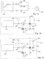
- Figure 14 shows a measurement principle that may be used to compensate a DC offset that may result from fluctuations of the light source intensity or of measurement parameters.
- the set-up is based on the principle of 'balanced detection'.
- a circulator 231 is used to direct the light portion coming back as a second output of the beam splitter/combiner 224 (to port II of the circulator) to a balanced detector where it is combined with the wanted signal S to interfere.
- the wanted signal S is an OCT signal obtained from interfering a signal combing back from a sample path sam and a signal coming back from a reference path ref.
- a beam splitter/combiner 224 is used to split the main beam between the sample path and the reference path and to combine them together to interfere.
- a deflector 235 is used to direct the signal beam onto a combiner 233 and two intensity detectors 221.1, 221.2. The intensity difference measured at the two detectors 221.1, 221.2 is used as the balanced signal.
- the circulator is operable to direct light entering port I to port II, light entering port II to port III, and light coming from port III to port I. In addition to serving to direct a second output of the beam splitter/combiner to the balanced detection set-up, it also serves as optical isolator keeping light from being fed back to the laser light source.
- the optical module shown in Figure 14 and comprising the light source 201 as well as the optical components of the wavemeter 208 (if present), of the beam splitter/combiner and the intensity detectors as well as potential beam directing means, may comprise a module casing in which the optical module components are arranged, the module casing comprising optical and electrical feedthroughs, like the devices illustrated in Figures 2 , 5 , 7 .
- the optical module components may be arranged on a common mount in contact with a common module thermoelectric cooler.
- Figure 15 depicts an optical module for an OCT device.
- the optical module comprises, preferably within a single module housing with feedthroughs and possibly with a common mount on a common cooler, in addition to the light source 201, the (optional) optical components of the wavemeter and the intensity detector(s) - in the depicted embodiment, two intensity detectors and a DC offset compensation arrangement as described hereinbefore are illustrated - the optical module also comprises the reference arm 257 of the OCT.
- the reference arm will comprise light deflecting and/or light guiding means 252, 253 that direct the reference light beam from the beam splitter/combiner 224 on an optical path with a defined optical length back to the beam splitter/combiner 224.
- FIG 16 yet depicts a dual beam swept source optical module for an OCT device.
- the dual beam swept source optical module comprises a single swept laser light source 201, preferably of the kind described as previous embodiments.
- the optical module may further comprise a wavemeter 202, 208 of the above-described kind.
- a beam splitter 251 is positioned downstream of the wavemeter (i.e. arranged after the wavemeter in a primary beam path) to split the primary beam into two partial beams, for example in a ratio of about 50:50.
- the two partial beams are used for individual OCT measurement of two separate OCT device branches.
- the two branches may be used to make an OCT image of the left and right eye, respectively.
- the OCT device then may be made as a kind of binocular-like device
- Each partial beam is directed onto a beam splitter/combiner 224.1, 224.2, and from there partial beam portions are directed on a sample arm and a reference arm, respectively.
- the reference arm may be within the optical module or, as depicted, comprise portions outside of the optical module.
- Light of the respective sample arm and the reference arm coming back to the beam splitter/combiners 224.1, 224.2 is brought to interfere, and then the intensity is measured in both branches individually.
- the branches may each comprise an intensity reference set-up as described referring to Fig. 14 . To that end, for each branch a portion of the light produced by the light source 201 is tapped (beam splitting taps for directing a small portion away are denoted by 231.1 and 232.2 in Fig.
- the tapping of the light portion from the primary beam may be upstream of the beam splitter (as illustrated) or also in each branch downstream of the beam splitter.
- reference number 250 schematically depicts a detection scheme. Also in Fig. 16 - like in all other embodiments - the detection may be based on a balanced heterodyne detection scheme that includes. To this end, an optical circulator may for example be present between the beam splitter 251 and each of the beam splitter/combiners 224,1, 224.2.
- the components illustrated to be within the casing 241 may be on a common mount and may be in thermal contact with a common thermoelectric cooler.
- the sequence of the taps with respect to a primary beam path may be reversed compared to the described embodiments.
- the monitor (if present) and/or the detector(s) (if present) need not necessarily be photodiodes but may be other suitable detectors for detecting light intensities.
- an optical isolator In the embodiments that integrate a part of an interferometer inside the optical module (such as the embodiments depicted in Figures 6 , and 14-16 ), it may be advantageous to provide an optical isolator. In such embodiments, absent an optical isolator, reflections from the sample and reference arm might travel back into the swept source laser.
- the optical circulators of the embodiments having a balanced detection scheme serves as such an optical isolator by keeping light incident on port II from being transmitted to port III.
- an optical isolator For embodiments that do not have the optical circulator, or in addition thereto, depending on the power level of those reflections it might be advisable to also integrate an optical isolator in order to protect the swept source laser.
- the optical isolator would be place, for example, in between the light source 201 and the beam splitter/combiner 224.An optical isolator may, like an optical circulator, be based on the Faraday rotator principle.
Description
- The invention is in the field of light sources, i.e. of sources of electromagnetic radiation in the infrared, visible, and ultraviolet part of the electromagnetic radiation spectrum. More concretely, the invention concerns a swept light source, such as for use in optical coherence tomography, and to a corresponding module.
- Optical Coherence Tomography (OCT) is an emerging technique for sub-surface imaging with medical, biological and other applications. OCT is the optical analog of ultrasound but takes advantage of the shorter wavelengths of light to achieve higher resolution images. Potentially the wavelength ranges of interest lie within the visible to near infrared regions of the spectrum from 400-2000nm. Currently, there are four wavelength ranges of interest in OCT centered around 850nm, 1050nm, 1300nm and 1550nm. OCT systems comprise (1) a broadband light source, (2) an arrangement of optical components for directing the emitted radiation to a sample and to a reference mirror and (3) an optical arrangement for measurement of interference of light reflected from the sample and light reflected from the reference mirror. For state-of-the-art Time Domain OCT (TD-OCT) systems, the broadband source is a superluminescent light emitting diode (SLED) which emits light in a broad spectrum of wavelengths (40-200nm bandwidth), and the sub-surface imaging depth is controlled by scanning the position of the reference mirror. Constructive interference only occurs when the path-lengths between the reference mirror and sample reflectors are equal within the coherence length of the light source. Fourier or Frequency domain OCT (FD-OCT) makes use of spectral frequency information, for example by decoding the interference using a dispersive element and a CCD detector array or Spectrometer (Spectral Domain OCT or SD-OCT). Another FD-OCT technique, requiring a simpler detection system, uses spectral encoding in time by spectrally scanning a narrow bandwidth light source (Swept Source OCT or SS-OCT).
- According to the state of the art, in SS-OCT, a tunable laser is used as the light source. SS-OCT has been demonstrated to have major signal to noise advantages over TD-OCT (see Choma et al, Optics Express, vol. 11, 2003 pp. 2183-2189). To realize its advantages over TD-OCT, swept source OCT systems require tunable light sources that can be swept across a wavelength range at high frequencies of 20-400kHz. Since the imaging depth required for the interferometers of these systems is related to the coherence length of the light source, this also sets the requirements for the linewidth and line spacing of the light source.
- Various methods have been employed to achieve swept sources for SS-OCT. Among these are cascaded Distributed Feedback (DFB) lasers (
US 2008/0037608 ), multi-wavelength lasers (US 2007/0002327 ), diffraction gratings and grating pairs (US 2008/0002209 ,US 7006231 ), fiber laser ring cavities (US 2006/0193352 ) external cavity lasers employing Fabry-Perot filter tuning elements in both ring and linear configurations (US 7242509 ,US 2006/0215713 ). Of these methods, the latter MEMS Fabry-Perot filter approaches are most applicable to integration within compact optical modules. In this case, the MEMS device performs both wavelength selection and wavelength sweep functions and needs to be manufactured to tight mechanical tolerances. The Fabry-Perot MEMS device is essentially a linear transducer that has speed limitations and is susceptible to variations in reflectivity, parallelism, flatness and filter cavity thickness over the tuning bandwidth. Variation in the latter parameter results in variation in bandwidth, coherence and imaging depth during a wavelength sweep of an SS-OCT system. - Another method (
US 2007/0183643 ) employs a MEMS tunable mirror integrated with a Vertical Cavity Surface Emitting Laser (VCSEL). Integration of these elements, however, is difficult to manufacture and has yet to be realized. - Simpler and more versatile designs are based on external cavity lasers where the filtering and wavelength sweep functions are performed by a grating and a rotating or scanning mirror (
US 6,111,645 ,US 5,907,423 ,US 2007/0276269 ,US 2007/0239035 ,US 2007/0064239 ,US 2008/0043244 ,US 2004/0213306 ). These designs are versatile, since they can relatively easily be adapted for other wavelength ranges. Swept-source OCT applications require the swept source to have a coherence length that is above a certain minimum value and below a certain maximum value. The minimum value is related to the minimum imaging range oft he application (imaging range is half the coherence length), for example 6 mm for retina imaging or up to 25 mm for imaging of the whole eye from the retina to the cornea. However, it would not be good to take a swept source that has a too long coherence length because then any kind of reflective object within the imaging range will cause unwanted interference signals. Therefore, multimode laser operation is required in order for the spectral bandwidth of the external cavity laser to have a certain minimum value. Single mode operation would not guarantee that the coherence length does not exceed a certain maximum acceptable value. A consequence of this minimum spectral bandwidth is a relatively long cavity length. In general this lies in a range 3-30 cm, depending upon the wavelength range and the number of modes in cavity. This cavity length requirement restricts the miniaturization of the swept source. Ideally, the swept source should easily be qualified and integrated into compact SS-OCT systems. Also, a too long cavity length makes the wavelength tuning slow limiting the sweep rate. - In
US 2008/0298402 A1 , an external cavity tuneable laser is disclosed which comprises a Fabry Perot etalon placed in the cavity which is structured and configured to define a plurality of equally spaced transmission peaks. Furthermore, an optical control ssytem is provided which comprises a first and a second photodetector placed on a beam splitter and a filter having a wavelength-dependent transmission placed between the beam splitter and the second photodetector, for determining the lasing wavelength. FromUS 2006/0215713 A1 , an external cavity laser is known which has a mirror-based resonant tunable filter, such as a Fabry Perot tunable filter. The laser can comprise a component in which the refractive index (n) can be changed, e.g., electrically, to thereby function as a cavity length controller. The component can be, e.g., an electro-optical, ceramic device that is electrically modulated in order to control the refractive index, so as to allow for the optical length of the cavity to be modulated. E.g., the cavity length is modulated with a high frequency source in order to scramble the cavity modes, or it is modulated in order to insure that a cavity mode overlaps with a reflection band of the tunable filter. - It is an object of the invention to provide a 'swept-source' light source for OCT or other applications of swept sources, that overcomes drawbacks of prior art light sources.
- In accordance with the invention, an optical module comprising a swept light source is provided as defined by
claim 1. - According to the invention, the swept light source comprises an optical retarding device as described hereinafter. In some embodiments, the swept light source comprises a folded cavity in which the light is directed back and forth on different path portions within the module casing a plurality of times.
- An optical feedthrough of the claimed optical module may comprise a fiber or a plurality of fibers, or it may comprise a window through which radiation is directed.
- An advantage of the approach according to a first aspect of the invention is that the light source components - and possibly elements of further devices such as intensity detector(s), beam splitter/combiner, a wavemeter and/or even a reference arm of an OCT set-up - are integrated in a common package. The devices integrated in the package preferably include the moving parts such as a MEMS grating or an MEMS mirror.
- The approach brings about advantages in terms of compactness, handling, manufacturing cost and calibration effort by the user. In accordance with preferred embodiments, the devices of the package have a common thermoelectric cooler that is in contact with a mount on which a plurality of the components within the module casing are arranged. This brings about further advantages in terms of stability and reproducibility as well as being advantageous in terms of manufacturing complexity.
- In contrast to optical packages as light sources of the prior art, the invention proposes to provide a swept light source with a wavelength selector (that may comprise a movable MEMS mirror and a grating or a Fabry-Perot filter tuning element (for example a Fabry-Perot MEMS device), or a rotating scanning mirror and a grating, etc.) and proposes, where it refers to light sources of a first type, multimode operation. Multimode operation makes possible that the coherence length can be controlled not to exceed a certain maximum acceptable value.. In addition, single mode operation - unless the cavity length is adjusted during tuning, which would require complicated set-up, mode hopping occurs: Mode-hopping means that the laser will turn off lasing operation for a short period of time and then turn on lasing operation again once the tunable filter coincides with the next lasing mode. The turn-on process of a laser, however, can be a relatively slow process (relative to the fast sweep rates that are required for SS-OCT applications) because stimulated laser emission has to build up from spontaneous emission and amplified spontaneous emission and therefore stable laser operation with low noise and good signal-to-noise ratio will require several round-trips in the laser cavity. Therefore, again, a multimode laser cavity is advantageous for fast wavelength tuning because the laser cavity can be kept lasing during the wavelength sweep. However, the laser cavity should not be too long (unless special techniques like Fourier-domain mode-locking (FDML) are used) because the associated long round-trip times would prohibit fast wavelength tuning again.
- Throughout this text, the term "light" is used to refer to electromagnetic radiation in the infrared, visible and ultraviolet part of the spectrum. The light source according to the invention is especially suited for producing light in the near infrared or visible part of the spectrum.
- The retarding device in embodiments of the invention thus is a part of an optical external cavity laser resonator. The optical path in the retarding device preferably constitutes a significant, substantial part of the optical resonator length. The path length in the retarding device (thus also the number of reflections) is well-defined by the arrangement. In a variant of the invention, the optical path length in the retarding device is at least 30%, at least 40% or at least 50% or 60% of the optical resonator length (the optical lengths being defined as the physical path lengths multiplied by the local index of refraction), and the number of passes within the retarding device is at least 4, preferably at least 6 or even 8 or more. In many embodiments, the fraction of the path length taken up in the retarding device is to be just high enough to enable the integration of an optical cavity within an optical package. There are embodiments of the optical retarding device in which the light traces within the device are not necessarily parallel. In general, a "pass" is a path portion inside the redarding device in between two subsequent reflections.
- The optical resonator length is between 1 cm and 1 m, in many cases between 3 cm and 30 cm.
- In embodiments of the invention, the gain device, the retarding device and the wavelength selector are arranged on the common base, and in many embodiments they are packaged, in an optical module package, to constitute an optical module. The optical module package forms a package housing with at least one optical feedthrough and with a plurality of electrical feedthroughs for feeding and controlling the components within the package and, if necessary, for reading out signals from within the package. The optical package for example comprises a common thermoelectric cooler, and the optical devices of the packaged are all in direct thermal contact with the thermoelectric cooler, i.e. are for example on a common heat conducting carrier plate that is in direct physical contact with the thermoelectric cooler. The optical package is for example closed - and possibly sealed - against the outside so that the components on the base are at most accessible by the electrical feedthroughs and/or the optical feedthroughs. The retarding device enables miniaturisation of the tunable external cavity arrangement so that it can be assembled into standard optical modules such as, for example, those known in the art as butterfly packages. The relatively simple optical arrangement is easily adaptable to operate at all the wavelength ranges of interest for SS-OCT by employing suitable gain blocks (or, as the case may be, resonator geometries of a free-space resonator) and optical coatings on components.
- Despite achieving multimode operation and according cavity dimension requirements, the dimensions of the overall package are compact, with a two-dimensionsal extension (in the plane of the mount) of preferably not greater than 22 mm*60 mm, in a preferred embodiment not greater than 13 mmx30 mm. For example, an overall extension is not greater than 22 mm*60 mm*20 mm, preferably not greater than 20 mm*40 mm*20 mm, especially not greater than 15 mm*35 mm*10 mm or not greater than 13 mm*30 mm*10 mm.
- In many embodiments of the invention, the retarding device comprises a plurality of reflective surfaces for reflecting back and forth light portions propagating in the block of material. The retarding device may be a block of material, for example of Silica or LiNbO3 or any other suitable material transparent for the light wavelengths concerned. The block may have two opposing surfaces that may be essentially parallel and that may be at least partially coated to be reflective. Suitable coatings may include metal coatings , dielectric coatings or other reflective layers. The light path within the retarding device may be defined by at least one of:
- the angle of incidence and geometrical optics, and
- a waveguiding structure formed within the block of material.
- In a special embodiment, the retarding device may comprise a circulating optical waveguide design.
- In an other embodiment, the retarding device comprises a body of a material transparent to the light to be used. The body has a plurality of plane facets that include facets that are at an angle different from 90° with respect to each other. At least two of the facets are at least partially reflective for the light in the resonator (by having a reflective coating and/or by the light impinging on a an angle shallow enough to exceed the angle of internal reflection) and reflect light impinging on the facet from an inside of the body back into the body. The body is designed and arranged so that the light path in the resonator is perpendicular to the respective end facet at non-reflective entrance and exit end facets (the distinction between the entrance and the exit is somewhat arbitrary: in the resonator the light will enter and exit both, through the entrance and the exit facets) and is non-perpendicular to the facets at least partially provided with a reflective coating.
- In preferred embodiments, the retarding device is designed so that at least one, preferably all reflections in the retarding device are caused by the light being incident on the facet at a low angle, for example below 50° or below the maximum angle for total internal reflection. By this measure, insertion losses that, for reflective coatings, are caused by the coatings being non-ideal are avoided. Also in these embodiments, the respective facets may in addition be provided with a highly reflective coating.
- The body of transparent material may for example be made of glass (a suitable material especially for embodiments where the light for being internally reflected impinges on a low angle), silica, a polymer, a semiconductor compound, etc.
- For example, the retarding device body has a generally rhomboid shape with a first facet and a second facet not parallel to the first facet. The retarding device is arranged so that the angle of incidence on the first facet is perpendicular. The light path in the retarding device is defined by geometrical optics. At an exit point of the light path from the retarding device, the second facet or the first facet comprises an angled portion so that the when exiting the light path is perpendicular to the surface through which it exits.
- In a further embodiment, the retarding device may comprise an optical waveguide design with waveguides defined at different vertical planes to enable longer beam path lengths in the retarding device. Such an optical waveguide design also facilitates coupling to optical components having optical axes at different levels.
- The retarding device may include one or more optical directional couplers. Such a directional coupler may be used for splitting the light in the retarding device between a resonator path and a monitoring path, between a sample output and a reference output, and/or also between an input and an imaging output.
- The wavelength selector, in embodiments of the invention, may comprise a scanning Micro-Opto-Electro-Mechanical Systems (MOEMS) mirror (sometimes also termed MEMS mirror) cooperating with a wavelength selective element, such as a grating. The MOEMS mirror and grating component are arranged to provide the tunable feature of the external cavity laser. The grating acts as a filter to select a narrow range of wavelengths for the cavity. The MOEMS mirror is scanned to vary the incident angle of light onto the grating such that the center wavelength of the narrow range of wavelengths can be varied. Alternatively, the grating could be integrated on the surface of the MOEMS scanning device.
- MOEMS devices (mirrors or, as an alternative for example also a MOEMS prism could be used) feature the advantage of having dimensions suitable for integration on the common base and in the optoelectronic package, without any negative influence on the overall size.
- Also, in some embodiments, the integrated swept wavelength light source also comprises a monitor, such as a monitoring photodiode, also arranged on the common base. The monitor is arranged so that a representative portion of the light circulating in the resonator is coupled out of the resonator and directed onto the monitor. The monitor comprises an electronic monitor output that is contactable by way of an electrical feedthrough from outside of the module so as to provide the possibility of an electronic control of the light source.
- In embodiments of the invention, which embodiments may, depending on the application, be advantageous, the gain device has reflective end facet that is used as resonator end mirror. For example, the partially transparent laser outcoupling mirror may be replaced by the (partially) reflective end facet of the gain device. Semiconductor gain devices with a reflective end facet correspond to reflective semiconductor optical amplifiers (R-SOAs). By the simple measure of using an R-SOA as both, gain device and outcoupling mirror, the efficiency of the device may be improved. This is because in a laser resonator, there are coupling losses when the light circulating in the resonator is coupled into gain device. If, instead of a gain device placed in an interior of the resonator, an R-SOA is used, the light has to be coupled into the gain device only once in every roundtrip in the resonator instead of twice. This may bring about a substantial reduction of the cavity loss and may therefore improve the swept-wavelength light source in power, tuning speed, tuning range, signa-to-noise ratio and/or other optical parameters.
- Now focusing on a second aspect of the invention, relating to light sources of second type, embodiments of the second aspect may be implemented according to one of the following designs:
- In a first arrangement type, the retarding device is positioned between the gain device and the wavelength selector;
- In a second arrangement type, the retarding device is positioned to one side of the gain block and the wavelength selector.
- In each case, "side" refers to an optical beam path in the resonator.
- In the case of the first arrangement type, the gain block used may be a reflective semiconductor optical amplifier (that in itself may be a resonator). Optical radiation propagates along a path which extends from the partially-reflective (for example 3-80%) facet of the R-SOA through the retarding device and is, for example, reflected by the MEMs mirror onto the grating. The optical path length between the R-SOA and the grating defines the length of the resonator (cavity) and the coherence properties of the swept source. The external cavity laser light is coupled to an optical fiber at the partially reflective semiconductor optical amplifier. Alternatively, in the case of the first arrangement, the gain block used may be a (non-reflective - for example <0.5%) semiconductor optical amplifier (SOA), a separate outcoupling mirror being provided. Embodiments with the R-SOA are, however, more compact.
- In the case of the second arrangement type, the gain block used may be a semiconductor optical amplifier (SOA). In this case optical radiation propagates along a path extending from a reflective coating on the retarding device through the SOA and is (for example) also reflected by the MEMS mirror onto the grating. The optical path length between the reflective coating of the retarding device and the grating defines the length of the cavity and the coherence properties of the swept source. The external cavity laser light is coupled to an optical fiber at the retarding device. In alternative embodiments, a separate outcoupling mirror on the other side of the retarding device (compared to the SOA) defines an end of the cavity.
- In a special embodiment of the second arrangement, the retarding device provides an additional interferometer with outputs that are coupled to an optical fiber or to a plurality of optical fibers.
- In embodiments of the invention, the light source may further comprise an electronic controller to regulate and adjust its performance. This may comprise a controlling device, for example including controlling electronic components and/or controlling software and/or firmware running on generic hardware, such as on a PC, a microprocessor, a microcontroller, or an FPGA. The controller is connected or connectable to the components on the base by electrical contact means, such as the electrical feedthroughs.
- The invention also concerns an optical coherence tomography apparatus, the apparatus comprising:
- a light source according to the invention;
- an interferometer in optical communication with the light source;
- an optics unit, the optics unit suitable for focussing a light portion originating from the light source onto a chosen location of a sample, and for performing a scan, in which said location and the sample are moved relative to one another;
- the interferometer being operable to combine a portion of light produced by the light source and returned from the sample with a portion of light produced by the light source and returned to the interferometer via a reference path; and
- a detector unit positioned to receive combined light from the interferometer.
- In this, "interferometer" refers to at least the portion of an interferometer that re-combines light coming from two paths. While other, physical definitions demand all elements that constitute the light paths - including the sample from which light portions are emitted back upon illumination, reflecting mirrors, and the detector - to belong to the interferometer, this is not the definition used in this text. In the following, therefore, the interferometer (or interferometer portion) that re-combines light coming from two paths is sometimes also referred to as "portion of an interferometer".
- As discussed above, there are embodiments of the light source, where the retarding device includes at least one directional coupler. These include embodiments where the directional coupler or one of the directional couplers comprises four waveguide branches:
- A first branch coupled to the resonator;
- A second and a third branch coupled to two output fibers, light coming from the first branch being split between the second and third branches; and
- A fourth branch coupled to a detector (such as a sensitive photodiode), wherein light portions coming from the second and third branches interfere in the directional coupler and some of the interfering light portions are coupled into the fourth branch (others might then be coupled back into the first branch).
- If the optical coherence tomography apparatus of the above-defined kind comprises a light source according to such an embodiment, the portion of the interferometer (being formed by the directional coupler) is integrated in the light source, and so is optionally the detector. Then, the optics unit may have to be merely provided with the integrated light source and detector module.
- The invention further also refers to an optical coherence tomography module for an optical coherence tomography apparatus, the module comprising:
- a light source according to the invention;
- In an embodiment, the module may, in addition to the light source, comprise:
- a portion of an interferometer in optical communication with the light source and operable to combine a portion of light produced by the light source and returned from a sample with a portion of light produced by the light source and returned from a reference path; and
- a detector unit (being the sensor arrangement or belonging to the sensor arrangement) positioned to receive combined light from the interferometer.
- In embodiments of the above-discussed kind with integrated interferometer and detector, the module is the integrated light source. In other embodiments, the module may, in addition to the packaged light source, comprise a separate, but potentially fixedly attached interferometer and detector.
- The module may further comprise, externally to the module casing, an electronics unit that includes an analyzer and/or evaluator for evaluating data produced by the sensor arrangement.
- The light source in accordance with any aspect of the invention may further incorporate measures for ensuring that the sweeping is linear or approximately linear. In a resonator, if the moving part(s) is/are just driven by an electrical signal linear in time, or of a resonant MEMS structure, for example driven by a clock-like signal to oscillate sinusoidally, is used, often a non-linear frequency dependency of the output radiation will result. A linear sweeping over time in the frequency domain (in k-space), however, is advantageous for OCT applications. The measures incorporated may include one or more of the following:
- (i) the moving part(s) of the wavelength selector (such as the MEMS mirror(s)) is/are driven with a characteristic ramp pattern in order to provide such linear sweeping in the frequency domain;
- (ii) The diffraction grating of the wavelength selector (in embodiments where the wavelength selector comprises a diffraction grating) as a non-constant pitch (grating constant) over the range the light beam is sweeping across. The non-constant pitch - a kind of special "chirp" - is chosen so that a more linear frequency sweep in time is achieved.
- (iii) The angle of incidence onto the grating is changed by an optical component between the moving part (the tuning element, e.g. mirror) of the light source and the grating. Such additional optical component would again change the sweep characteristics over time and make it more linear in the frequency domain.
- The electronics unit of the claimed module may be configured to calculate the quantity (IT-IR )/(IT +IR ) from which, given the known or initially measured filter characteristics, the wavelength or a related quantity may be calculated.
- The filter device is chosen so that in the light source wavelength range, in which the light source output wavelength sweeps, the filter characteristics has a pronounced wavelength dependence. Preferably, in the light source wavelength range, the filter transmission characteristic is a strictly monotonous function of the wavelength. The difference between the transmission at the lowest wavelength of the wavelength range, and the transmission of the highest wavelength of the wavelength range is then preferably as high as possible. The filter may be a high-pass filter or a low-pass filter. However, a in preferred embodiments, the filter is a bandpass filter, the passband of which is offset relative to the wavelength range, so that the wavelength range is in a sloped portion of the filter transmission characteristics. There are bandpass filters available that have, within the wavelength range used for example for swept-source OCT, a steep characteristic.
- In prior art of SS-OCT systems an optical filter with a periodic transmissive or reflective response in the frequency domain (k-space), for example a Mach-Zehnder interferometer or a Fabry-Perot filter, is used to generate an optical k-clock, that is a signal that exhibits a local maximum or peak each time the swept source has changed the frequency by a fixed amount that is identical to the free-spectral range of such periodic optical filter. This optical k-clock signal is detected by a photodetector and converted into an electrical k-clock signal that is then synchronized with other clock signals of the SS-OCT system responsible, for example, for sampling the received OCT signal from the interferometer.
- In contrast to prior art wavemeters, that for example are based on the Michelson or Fizeau interferometer principle, however, the proposed wavemeter according to the third aspect of the invention is simple, robust, has not moving parts, and the output signals are easy to analyze.
- Also, the signal from the wavemeter is independent of the optical output power of the swept laser and hence a true meausure of the wavelength or frequency.
- In contrast to k-clocks of prior art OCT modules, a measure for the absolute value of the wavelength is measured, and not only a relative measure. Further, the measurement of the wavelength values can be done at any time, i.e. with any sampling rate set by a separate clock. Thus, it is possible to use a clock (system clock) that is used for sampling the measurement of the signal, for example the intensity I of an OCT interference signal to be measured, or an other clock in time with such a system clock. Synchronization of the device is much easier than in prior art approaches where the signal peeks of the k-clock itself had to serve as synchronizing signal. If the wavemeter is sampled synchronously with the wanted signal, one obtains directly data pairs of (wanted) intensity data and of the wavelength at which the wanted intensity data was generated.In accordance with a preferred embodiment, the electronics unit of the module thus further comprises a clock, the clock being operable to trigger a sampling of the first and second wavemeter detector signals. The clock may further be operable to trigger a sampling of a wanted intensity signal.
- It has been known to use wavelength selective filters for stabilizing lasers. Embodiments of the invention, however go in an other direction by proposing to use it such a filter as a component of a wavemeter that can be sampled synchronously with the signal.
- Embodiments of optical modules according to the invention may further optionally comprise one or a combination of the following:
- a DC signal offset compensation: Such a DC signal offset compensation may be based on the principle of heterodyne balanced detection. It may eliminate the effect of primary light source intensity variations, that for example may arise periodically with the sweeping frequency (if the produced radiation intensity has some wavelength dependence) or slowly as a reaction to changing parameters such as a temperature change etc. For example, the two outputs of the beam splitter/combiner may be used and directed at two detectors, and the measured intensities at these detectors are subtracted from each other. Since the interference signal occurs 180° degrees out of phase at the two detectors, subtracting the two signals adds the heterodyne interference signal but subtracts excess noise.
- A beam splitter/combiner of an OCT device (OCT interferometer) that is used to split a primary beam between a sample arm and a reference arm and to combine light portions coming back from the sample arm and the reference arm and to direct combined, interfering light portions onto a wanted signal intensity detector (which detector is preferably also an element of the optical module). Optionally, the optical module may further comprise the reference arm with light deflecting and/or light guiding means that direct the reference light beam from the beam splitter/combiner on an optical path with a defined optical length back to the beam splitter/combiner. By this, the optical module may become an 'OCT engine', i.e. a device that outputs a sample radiation (of an OCT interferometer sample arm) and comprises the means for bringing to interfere and analyzing the radiation coming back from the sample in the sample arm.
- A beam splitter, for example of equal or approximately equal intensity. The module may then further comprise two beam splitters/combiners and twice according detection means (that optionally may include DC offset compensation) and, optionally, two reference arms, as well as according optical (and electrical) output/inputs. By this, the optical module is suitable of simultaneously carrying out two OCT measurements by means of a single light source.
- All of these optional features may be incorporated in a package - and within a module housing and preferably on a common mount and in thermal contact with a common thermoelectric cooler of the compact optical module.
- While the light sources and optical modules according to the aspects of the invention in this text are primarily described referring to the important application of OCT, they may also advantageously be used for other applications. Such other applications for example include Fiber Bragg Interrogators etc.
- In the following, embodiments and aspects of the invention are described referring to drawings. The drawings are all schematic and not to scale, and same reference numerals refer to same or analog elements. The drawings show:
-
Fig. 1 . represents a pictorial view of the optical arrangement using an R-SOA; -
Fig. 2 shows a pictorial view of the assembly of the optical arrangement in an optical module; -
Fig. 3 is a pictorial view of the optical arrangement with monitor diode repositioned; -
Fig. 4 shows a pictorial view of the optical arrangement using an SOA; -
Fig. 5 represents the pictorial view of the assembly of the optical arrangement with SOA in an optical module; -
Fig. 6 shows the pictorial view of the optical arrangement using an SOA with integrated interferometer; and -
Fig. 7 shows a pictorial view of the optical arrangement with interferometer in an optical module -
Figs. 8, 9a ,9b, and 9c depict embodiments of a retarding devices; -
Fig. 10 shows a non-claimed example of a light source without a retarding device; -
Fig. 11 shows an optical module with a wavemeter according to the third aspect of the invention; -
Fig. 12 depicts a schematical representation of a wavelength dependent filter transmission characteristic; -
Fig. 13 shows a scheme of an optical module according to the third aspect; -
Fig. 14 depicts an optical module with a DC offset compensation; -
Fig. 15 shows and optical module with a reference arm; and -
Fig. 16 depicts a dual beam OCT module. - A first embodiment of the invention is an optical arrangement as shown in
Figure 1 . In this embodiment, the optical arrangement comprises anoptical retarding device 100 havingreflective coatings 101 at opposing facets, anoptical gain block 102,scanning MEMS mirror 103,diffraction grating 104,monitor photodiode 105, a gainblock coupling lens 106 and alens 107 that may be collimating or imaging the beam. - In this embodiment and in other depicted embodiments, the resonator design ins based on the so-called Littrow configuration, where the diffraction grating acts as a resonator mirror. However, the invention, pertaining to all embodiments, is not restricted to such configuration. The skilled person will know other resonator configurations of tunable resonators for externa-cavity diode lasers. An other known configuration is the so-called Littman-Metcalf configuration where a separate mirror (that may be the movable device), onto which diffracted radiation is directed, is used as an end mirror. The skilled person will know ways to re-arrange resonator components in a manner that the grating is not a resonator end mirror.
- In this embodiment, the gain block is preferably a reflective-semiconductor optical amplifier (R-SOA) having a broad gain bandwidth of 40-200nm. The R-SOA has a reflective coating on the
face 110 away from the optical retarding device. Theoptical retarding device 100 is preferably made using a block of, silica, or of glass, polymer, or a semiconductor compound that hasmirror layers 101 deposited on its parallel surfaces. The mirror layers are preferably defined such that only parts of the parallel surfaces where the optical beam is retarded are coated. Other parts of the parallel surfaces may be coated with an anti-reflection coating. InFig.1 a retarding device is illustrated providing eight reflections in the optical path resulting in nine passes of the retarding device. Alternatively a retarding device can be so used to provide any number of reflections as required for the cavity length of the tunable laser. The optical path in the optical retarding device may optionally be defined by waveguides formed in the block. Such waveguides (this pertains to all embodiments with waveguides in the retarding device block) may have been directly written in the silica, for example by means of a femtosecond pulsed laser. - In another embodiment of the invention the optical retarding device may be made from lithium niobate or any other suitable material.
- The optical arrangement forms a tunable external cavity laser of the first above-mentioned type. Light produced in the
gain block 102 oscillates in the resonator defined by thereflective coating 110 on thegain block 102 and the grating 104 (The cavity of the external cavity laser extends between the front facet of the R-SOA 110, that here functions as the outcoupling mirror, and the diffraction grating 104). Thelens 107 is used to collimate light between the retardingdevice 100 and the wavelength selector (that comprises theMEMS mirror 103 and the grating 104, whereas the gain block coupling lens images between the gain block and the optical retarding device. Alternatively, thelens 107 is used to image the light onto the MEMS mirror such that the image size changes betweenlens 107,MEMS mirror 103 anddiffraction grating 104. More in general, any suitable arrangement of imaging and/or collimating means (that may, in addition or as alternative to lenses may include appropriately shaped reflectors) and, if necessary, radiation directing means, may be used. Alternatively to lenses, optical waveguide tapers may be provided by the retarding device to couple light directly to the gain block. - The MEMS mirror used in this embodiment (and other embodiments described herein) preferably scans at frequencies of 20-400kHz and is driven by either a resonant or linear ramp waveform.
- The monitor diode is arranged in a position where it is hit by light portions different from the light portions directed back into the resonator by the grating; for example when the -1st diffraction order is directed back into the resonator, the 1st diffraction order or the 0th diffraction order may be directed onto the
monitor diode 105. - Light from the laser is coupled by a
coupling lens 108 into anoptical fiber 109. -
Figure 2 is a view of the assembly of the external tunable laser into a module. Preferably the R-SOA 102 is mounted on afirst submount 111 and thefiber 109 is mounted on asecond submount 112. Bothsubmounts optical module casing 115. The optical module casing may be a butterfly package casing as illustrated inFig.2 . In another embodiment of the invention, the optical module may be a DIL (dual in line) package or other optical module. Thefiber 109 may be fixed to themodule feedthrough 116 with aferule 117. Alternatively the fiber may be fixed to the feedthrough directly. The module comprises also a plurality ofelectrical feedthroughs 119 for supplying, controlling and tapping the devices in the module. - In another embodiment of the invention, the
carrier 113 may be made from two plates whereby a smaller plate is mounted on a larger plate to facilitate mounting of bases of the optical components at different levels to align their optic axes. Alternatively a carrier with different mounting levels machined into its surface may be used. -
Figure 3 illustrates another embodiment of the present invention that is similar to the embodiment ofFig. 1 in that it also corresponds to the first type of arrangements. The elements that have the same function as the ones inFig. 1 are not explained again here. In the embodiment ofFig. 3 , themonitor photodiode 105 is positioned on the same side of the retarding device as the R-SOA 102. In this embodiment, theretarding device 118 is made and positioned so that the optical beam is partially reflected and partially transmitted at one interface so that this may be imaged onto themonitor diode 105. For this embodiment, a partially reflective coating may be used at thepart 120 of the face of the retarding device where the optical beam passes through to the monitor diode. - Another arrangement, corresponding to the second type, of the external cavity laser is pictured in
Figures 4 and5 . This embodiment provides adifferent retarding device 122, which is positioned to one side of thegain block 121,diffraction grating 104 andMEMS mirror 103. Thegain block 121 in this case is a semiconductor optical amplifier (SOA) having anti-reflection coatings on both its facets. - The optical cavity of this arrangement extends from the point A at
reflector 101 to the grating 104 (the retarding device is thus passed eight times). In this embodiment, the retarding device is made preferably using waveguides such that light impinges perpendicularly at point A and for example also at the outputs of theretarding device 122 to theoptical fiber 109 and to themonitor photodiode 105. - Light portions reflected at point A are split between a portion directed back into the resonator and a portion that is directed to the outputs. In the depicted embodiment, this output portion is further split between a portion coupled into the
fiber 109 and a portion caused to impinge on the monitor diode. - Here, the splitting between the respective portions is achieved by a first directional coupler 131 (waveguide coupler) and a second
directional coupler 132, both formed in theretarding device 122. In an alternative arrangement, the splitting functionality could also be achieved by partially transparent mirrors, for example a partially transparent mirror reflecting back a portion of the radiation into the resonator and coupling out an other portion; the monitor diode may then be placed like inFig. 1 orFig. 3 . - Additionally it is possible to provide a retarding device having optical waveguide tapers to couple light directly to the gain block. It is also possible to provide a retarding device having optical waveguide tapers to couple light directly to optical fiber.
- It is possible to use waveguides for only a portion of the beam path in the retarding device, or for the whole beam path in the retarding device.
- It is further possible to provide a retarding device where at least a part of the beam path is defined by a waveguide also in arrangements of the first type, for example according to
Fig. 1 or according toFig. 3 . - Even further, it would also be possible to provide an arrangement of the second type where the retarding device does not comprise any waveguide, but where the split between the output and light reflected back into the resonator is achieved by other means, such as by a partially transparent mirror.
- An advantage of the arrangement shown in
Fig. 4 is that the optical power measured by the photodiode is directly proportional to the output power of the external cavity laser. -
Figures 6 and7 show another embodiment of the invention which provides additional optical waveguides in the optical retarding device. Here theretarding device 123 includes a thirddirectional coupler 133 with a first waveguide branch 133.1 (input waveguide) optically-coupled to the external cavity laser and fed by the light coupled out of it, a second and third waveguide branch 133.2, 133.3 (output waveguides) which are optically coupled to twooptical fibers 124 and a fourth waveguide branch 133.4 which leads to areference photodiode 125. - In this embodiment, the third
directional coupler 133 has a double function. Firstly, it splits light coming on the input branch 133.1 from the laser to the two output waveguide branches 133.2, 133.3 and thus between the twooptical fibers 124 that for example lead to the sample and reference arm of the OCT device, respectively. Secondly, it interferes light coming back from the twofibers 124 via the second and third waveguide branches, respectively. It thus acts as interferometer. The optical fibres act as sample and reference arms of this interferometer which forms part of a Swept Source OCT system, and thereference photodiode 125 for example acts as the detecting device of the OCT system. - This subsystem may be integrated in an optical module having one
feedthrough 116 as shown inFig. 7 . Alternatively, the optical module could include a plurality of optical feedthroughs. - In
Figures 8, 9a ,9b, and 9c , variants of optical retarders that may be used in any embodiment of a multimode swept laser light source that comprises a retarder are depicted. As can be seen inFigures 8 9a ,9b, and 9c , theretarders -
Figures 9b and 9c show variants of optical retarders which may be used in any embodiment of a multimode swept laser light source. As can be seen fromFigures 9b and 9c , theseretarders facets 101a which are mutually arranged such that a beam may impinge on the retarder at a right angle and then be reflected at each of the angled facets under a low angle. Preferably the facets are arranged at angles exceeding a critical angle at which an incoming beam is totally internally reflected. Thefacets 101a may be defined with or without high-reflectivity coatings. The retarder depicted inFigure 9c may be used together with anexternal reflector 101b such that a beam enters and leaves the retarder more than once, every time preferably at a right angle. - The skilled person will realize that the concept of having a body with more than six plane facets that include facets at an acute angle will, by application of geometrical optics, yield a plurality of further variants of retarder shapes that all ensure right entrance and exit angles in combination with a well-defined number of transitions through the body.
-
Figure 10 shows an unclaimed variant of a multimode external cavity swept laser light source that comprises, in an optical module casing, again device 121, awavelength selector light re-directors 104; 106, 107. In contrast to the hereinbefore-described embodiments, the resonator does not comprise an optical retarder but is folded to have a sufficient cavity length corresponding to a plurality of module lengths. - In the depicted embodiment, the
gain device 121 is an SOA, thus a gain block where neither of the facets reflects light back into the device. For example, the facets may be at a non-perpendicular angle to the beam direction and/or the facets may comprise AR coatings, etc. - However, it would also be possible to provide light source without retarder of the kind shown in
Figure 10 with an RSOA gain element, for example at the position of theoutcoupling mirror 140. The advantage would be the same as for devices with optical retarder: the reduction of coupling losses. - Referring to
Figures 11, 12 and13 , a concept of a wavemeter of a swept light source according to the third aspect of the invention is described. In analizing data obtained by measurement devices with swept light sources, it is in most cases important to know which data point corresponds to which wavelength of light produced by the swept source. In prior art Optical Coherence Tomography (OCT) devices - and similar devices - therefore, a so-called k-clock is used for data sampling. The letter 'k' in this is used to refer to the wavenumber k that is proportional to the inverse of the wavelength and, in a given medium, is thus proportional to the frequency. The k-clock of prior art devices comprises a Fabry-Perot filter or the like through which a portion of the generated light is directed. The signal transmitted through the filter will have a characteristic dependency on the frequency with a pattern of peeks in regular frequency distances of for example 25 GHz. The peeks are then used to trigger sampling of the actual signal. This way to proceed has two disadvantages. Firstly, the absolute wavelength position is not know but only the relative peek-to-peek distance. Secondly, the peek-to-peek frequency distance - the free spectral range of the Fabry-Perot filter - is fixed. However, given a usually non-linear output-frequency - time relationship, the sampling will be at irregular time intervals, and this produces non-trivial synchronization problems. -
Figure 11 depicts a wavemeter of a device according to the third aspect of the invention. Theblock 201 denotes the swept light source, which may be a light source according to one or both of the hereinbefore described aspects of the invention. Although thelight source 201 is shown in this figure and in subsequent figures as block separate from the further elements, in practice also the further elements can be integrated in the package that comprises the light source, and the further elements can be arranged physically between elements of the light source (but not, of course, interrupting the beam path within the resonator of the light source) or in separate positions. By means of a beam splitter 202 a portion - for example between 1% and 10% of the beam is 'tapped', i.e. directed away from the main beam and onto the wavemeter. - The wavemeter comprises a
filter device 204 on which the tapped beam portion impinges. The filter in the depicted embodiment is a bandpass filter, the passband of which is offset relative to the wavelength range, so that the wavelength range is in a sloped portion of the filter transmission characteristics. -
Figure 12 shows a schematic dependence of a relative filter transmission power (intensity transmission coefficient) on the wavelength. The vertical lines schematically depict the upper and lower limits of the wavelength range. - Returning to
Fig. 11 , in addition to thefilter device 204, the wavemeter comprises a firstlight intensity detector 206 and a secondlight intensity detector 207. The first light intensity detector is configured and arranged to detect light of the tapped beam that is transmitted through the filter. The secondlight intensity detector 207 is configured and arranged to detect light portions that are not transmitted by thefilter 204 and are consequently reflected by it. - Because of the dependence of the transmitted intensity on the wavelength, the quantity IT-IR being the difference between the intensity IT, measured by the first
light intensity detector 206 and the intensity IR measured by the secondlight intensity detector 207 is a measure of the wavelength. Preferably, the normalized value (IT-IR )/(IT +IR ) is used as an input quantity for determining, using the known filter characteristics, the wavelength. The filter characteristic can be, based on an initial measurement, for example by the manufacturer, stored in the device's electronics. It would also be possible to use the quantity (IT -IR )/(IT +IR ) itself as a measure of the wavelength. - Because of this approach, the absolute value of the wavelength is known, and not only a relative measure. Further, the measurement of the wavelength values can be done at any time, i.e. with any sampling rate set by a separate clock. Thus, it is possible to use the system clock or an other clock in time with such a system clock. Synchronization of the device is much easier than in prior art approaches where the signal peeks of the k-clock itself had to serve as synchronizing signal.
-
Figure 13 very schematically illustrates an according measurement system. Thesystem clock 211 provides a trigger signal for reading out the measurement values of the first and secondwavemeter intensity detectors signal intensity detector 221. The system electronics calculates the wavelength from the wavemeter intensity detector signals and stores the intensity/wavelength data pairs; these values may be displayed and/or used in further calculations as known in the art. In reality, for each detector an analog/digital converter triggered by the trigger signal may be used to read out the signals. Also, the clock trigger signal may be used also for sampling further signals, and/or the wanted signal may be obtained from a plurality of detector signals, as for example in the embodiment described hereinafter. -
Figure 14 shows a measurement principle that may be used to compensate a DC offset that may result from fluctuations of the light source intensity or of measurement parameters. The set-up is based on the principle of 'balanced detection'. In the depicted embodiment, acirculator 231 is used to direct the light portion coming back as a second output of the beam splitter/combiner 224 (to port II of the circulator) to a balanced detector where it is combined with the wanted signal S to interfere. In the depicted embodiment, the wanted signal S is an OCT signal obtained from interfering a signal combing back from a sample path sam and a signal coming back from a reference path ref. In the depicted embodiment, a beam splitter/combiner 224 is used to split the main beam between the sample path and the reference path and to combine them together to interfere. Adeflector 235 is used to direct the signal beam onto acombiner 233 and two intensity detectors 221.1, 221.2. The intensity difference measured at the two detectors 221.1, 221.2 is used as the balanced signal. The circulator is operable to direct light entering port I to port II, light entering port II to port III, and light coming from port III to port I. In addition to serving to direct a second output of the beam splitter/combiner to the balanced detection set-up, it also serves as optical isolator keeping light from being fed back to the laser light source. - In
Figure 14 , the -optional wavemeter 208 of the kind described referring toFigures 11-13 is illustrated by dashed lines. - The optical module shown in
Figure 14 and comprising thelight source 201 as well as the optical components of the wavemeter 208 (if present), of the beam splitter/combiner and the intensity detectors as well as potential beam directing means, may comprise a module casing in which the optical module components are arranged, the module casing comprising optical and electrical feedthroughs, like the devices illustrated inFigures 2 ,5 ,7 . The optical module components may be arranged on a common mount in contact with a common module thermoelectric cooler.Figure 15 depicts an optical module for an OCT device. The optical module comprises, preferably within a single module housing with feedthroughs and possibly with a common mount on a common cooler, in addition to thelight source 201, the (optional) optical components of the wavemeter and the intensity detector(s) - in the depicted embodiment, two intensity detectors and a DC offset compensation arrangement as described hereinbefore are illustrated - the optical module also comprises thereference arm 257 of the OCT. The reference arm will comprise light deflecting and/or light guiding means 252, 253 that direct the reference light beam from the beam splitter/combiner 224 on an optical path with a defined optical length back to the beam splitter/combiner 224. The embodiment ofFigure 15 - as well as an according variant of a dual beam swept source optical module as described further below but with an integrated reference arm - is advantageous because of its compactness in cases the overall OCT device is small, for example in a hand-held device where the distance to the measured object is small. -
Figure 16 yet depicts a dual beam swept source optical module for an OCT device. The dual beam swept source optical module comprises a single sweptlaser light source 201, preferably of the kind described as previous embodiments. The optical module may further comprise awavemeter beam splitter 251 is positioned to split the primary beam into two partial beams, for example in a ratio of about 50:50. The two partial beams are used for individual OCT measurement of two separate OCT device branches. For example, the two branches may be used to make an OCT image of the left and right eye, respectively. The OCT device then may be made as a kind of binocular-like device - Each partial beam is directed onto a beam splitter/combiner 224.1, 224.2, and from there partial beam portions are directed on a sample arm and a reference arm, respectively. The reference arm may be within the optical module or, as depicted, comprise portions outside of the optical module. Light of the respective sample arm and the reference arm coming back to the beam splitter/combiners 224.1, 224.2 is brought to interfere, and then the intensity is measured in both branches individually. Optionally, the branches may each comprise an intensity reference set-up as described referring to
Fig. 14 . To that end, for each branch a portion of the light produced by thelight source 201 is tapped (beam splitting taps for directing a small portion away are denoted by 231.1 and 232.2 inFig. 16 ), and the intensity detecting means of each branch comprise two intensity detectors 221.1, 221.2; 221.3,. 221.4. The tapping of the light portion from the primary beam may be upstream of the beam splitter (as illustrated) or also in each branch downstream of the beam splitter. - In
Figure 16 ,reference number 250 schematically depicts a detection scheme. Also inFig. 16 - like in all other embodiments - the detection may be based on a balanced heterodyne detection scheme that includes. To this end, an optical circulator may for example be present between thebeam splitter 251 and each of the beam splitter/combiners - Also in the embodiment of
Figure 16 , the components illustrated to be within the casing 241 (that has optical and electrical feedthroughs just like in the previously described embodiments) may be on a common mount and may be in thermal contact with a common thermoelectric cooler. - In all embodiments that comprise both, a tap for the wavemeter and at least one tap for the intensity reference, the sequence of the taps with respect to a primary beam path may be reversed compared to the described embodiments.
- In all embodiments, the monitor (if present) and/or the detector(s) (if present) need not necessarily be photodiodes but may be other suitable detectors for detecting light intensities.
- In the embodiments that integrate a part of an interferometer inside the optical module (such as the embodiments depicted in
Figures 6 , and14-16 ), it may be advantageous to provide an optical isolator. In such embodiments, absent an optical isolator, reflections from the sample and reference arm might travel back into the swept source laser. The optical circulators of the embodiments having a balanced detection scheme serves as such an optical isolator by keeping light incident on port II from being transmitted to port III. For embodiments that do not have the optical circulator, or in addition thereto, depending on the power level of those reflections it might be advisable to also integrate an optical isolator in order to protect the swept source laser. The optical isolator would be place, for example, in between thelight source 201 and the beam splitter/combiner 224.An optical isolator may, like an optical circulator, be based on the Faraday rotator principle. - It would be possible to provide the functionalities of the optical modules described referring to
Figures 11-16 also using waveguide technology, for example in a photonic light wave circuit PLC.
Claims (9)
- An optical module comprising an optical module casing (155) and a swept light source (201) in the optical module casing (115), and an electronics unit capable of controlling the swept light source (201) and/or of analyzing a signal from a detecting means (221, 253) of the optical module, the module further comprising a wavemeter (208), the wavemeter (208) comprising:- a wavemeter tap (202) capable of directing a wavemeter portion of light produced by the light source (201) away from a main beam,- a wavelength selective filter (204) arranged to receive the wavemeter portion,- a first wavemeter detector (206) arranged to measure a transmitted radiation intensity of radiation transmitted through the filter, and- a second wavemeter detector (207) arranged to measure a non-transmitted radiation intensity of radiation not transmitted through but reflected by the filter,wherein the wavemeter tap (202), the wavelength selective filter (204), the first wavemeter detector (206) and the second wavemeter detector (207) are preferably arranged in the module casing (115);
wherein the swept light source (201) is a light source of a first type or a light source of a second type, a light source of the first type comprising- the optical module casing (115) with at least one optical feedthrough (116) and a plurality of electrical feedthroughs (119),- a semiconductor gain device (102, 121) operable to provide light amplification;- a wavelength selector (103,104); and- light re-directors (106,107);the gain device (102, 121), the light re-directors (106,107) and the wavelength selector (103,104) being mutually arranged in the optical module casing (115) so that a multimode resonator is established for light portions emitted by the gain device (102, 121) and selected by wavelength selector (103,104); wherein the resonator is an external cavity laser resonator, the resonator comprising an optical retarding device, the retarding device comprising a block of material, a beam path with a well-defined beam path length being defined for light within the block of material produced by the gain device and circulating in the resonator, an optical resonator length of the resonator being between 1 cm and 1 m; and
wherein one end reflector (110) of the resonator is partially transmitting and wherein light transmitted through this one end reflector (110) is at least partially directed to exit through the optical feedthrough (116);
a light source of the second type comprising- a semiconductor gain device (102, 121) operable to provide light amplification;- an optical retarding device (100, 118, 122, 123), the retarding device comprising a block of material, a beam path with a well-defined beam path length being defined for light within the block of material produced by the gain device (102, 121);- a wavelength selector (103,104); and- a base (113);the gain device (102, 121), the retarding device (100, 118, 122, 123) and wavelength selector (103,104) being mutually arranged on the base (113) so that a resonator is established for light portions emitted by the gain device (121) and selected by wavelength selector (103,104), an optical resonator length of the resonator being between 1 cm and 1 m;
wherein the beam path in the retarding device (100, 118, 122, 123) is a part of a beam path of the resonator; and
wherein at least one of the following applies for a light source of the first type and for a light source of the second type:- an optical beam path length in the retarding device constitutes at least 30% of optical resonator length, wherein said light within the block of material makes, along said beam path, at least four passes, wherein a pass is a path portion inside the retarding device in between two subsequent reflections; and- the retarding device has a plurality of plane facets that include facets that are at an acute angle with respect to each other, wherein at least two of the facets are at least partially reflective and reflect light impinging on the at least partially reflective facet from an inside of the body back into the body, wherein the body is designed and arranged in the resonator so that the light path in the resonator is perpendicular to non-reflective entrance and exit end facets and is non-perpendicular to reflective facet portions upon which it impinges. - The optical module according to claim 1, wherein the electronics unit is equipped for comparing and analyzing signals of the first and second wavemeter detectors (206,207), wherein the analysis of the signals comprise evaluating the value (IT-IR )/(IT+IR ), where IT is the intensity measured by the first light intensity detector (206) and IR is the intensity measured by the second light intensity detector (207).
- The optical module according to claim 2, wherein the electronics unit comprises a clock, the clock being operable to trigger a sampling of the first and second detector signals.
- The optical module according to any one of the preceding claims, wherein in case the swept light source (201) is a light source of the first type, the light source comprises a common thermoelectric cooler (114) in thermal contact with at least the semiconductor gain device (121) and the wavelength selector (103,104), and wherein in case the light source (201) is a light source of the second type, the light source comprises a thermoelectric cooler (114) connected and thermally coupled to the base (113).
- The optical module according to any one of the preceding claims, wherein the wavelength selector comprises a MEMS movable device (103).
- The optical module according to claim 5, wherein the wavelength selector comprises a MEMS mirror (103) and a diffraction grating (104), the MEMS mirror (103) operable to scan an incident angle of a light beam on the diffraction grating (104), or wherein the wavelength selector (103) comprises an integrated MEMS grating-mirror device (103), in particular wherein the grating is chirped.
- The optical module according to claim 6, wherein the diffraction grating (104) or the integrated MEMS grating-mirror device (103), respectively, defines an end face of the resonator.
- The optical module according to any one of the preceding claims, wherein the semiconductor gain device (121) is chosen from a group comprising a semiconductor amplifier and a reflective semiconductor amplifier, in particular wherein the semiconductor gain device (121) is a reflective semiconductor amplifier and a reflective coating of the reflective semiconductor amplifier is a resonator end mirror, for example an outcoupling mirror, of the resonator.
- The optical module according to any one of the preceding claims, further comprising an optical fiber (109) optically coupled to an output of the resonator.
Applications Claiming Priority (2)
| Application Number | Priority Date | Filing Date | Title |
|---|---|---|---|
| US16647009P | 2009-04-03 | 2009-04-03 | |
| PCT/CH2010/000015 WO2010111795A1 (en) | 2009-04-03 | 2010-01-22 | Light source, and optical coherence tomography module |
Publications (2)
| Publication Number | Publication Date |
|---|---|
| EP2415131A1 EP2415131A1 (en) | 2012-02-08 |
| EP2415131B1 true EP2415131B1 (en) | 2020-10-28 |
Family
ID=42062009
Family Applications (1)
| Application Number | Title | Priority Date | Filing Date |
|---|---|---|---|
| EP10701611.5A Active EP2415131B1 (en) | 2009-04-03 | 2010-01-22 | Light source, and optical coherence tomography module |
Country Status (5)
| Country | Link |
|---|---|
| US (2) | US8625650B2 (en) |
| EP (1) | EP2415131B1 (en) |
| JP (1) | JP5738271B2 (en) |
| CN (1) | CN102484353B (en) |
| WO (1) | WO2010111795A1 (en) |
Families Citing this family (93)
| Publication number | Priority date | Publication date | Assignee | Title |
|---|---|---|---|---|
| US9867530B2 (en) | 2006-08-14 | 2018-01-16 | Volcano Corporation | Telescopic side port catheter device with imaging system and method for accessing side branch occlusions |
| WO2009009799A1 (en) | 2007-07-12 | 2009-01-15 | Volcano Corporation | Catheter for in vivo imaging |
| US9596993B2 (en) | 2007-07-12 | 2017-03-21 | Volcano Corporation | Automatic calibration systems and methods of use |
| WO2009009802A1 (en) | 2007-07-12 | 2009-01-15 | Volcano Corporation | Oct-ivus catheter for concurrent luminal imaging |
| US8259303B2 (en) | 2008-05-15 | 2012-09-04 | Axsun Technologies, Inc. | OCT combining probes and integrated systems |
| WO2010111795A1 (en) * | 2009-04-03 | 2010-10-07 | Exalos Ag | Light source, and optical coherence tomography module |
| JP4991834B2 (en) | 2009-12-17 | 2012-08-01 | シャープ株式会社 | Vehicle headlamp |
| JP5232815B2 (en) * | 2010-02-10 | 2013-07-10 | シャープ株式会社 | Vehicle headlamp |
| US8733996B2 (en) | 2010-05-17 | 2014-05-27 | Sharp Kabushiki Kaisha | Light emitting device, illuminating device, and vehicle headlamp |
| CN104482477A (en) * | 2010-05-17 | 2015-04-01 | 夏普株式会社 | Illuminant and light-emitting device |
| US9816677B2 (en) | 2010-10-29 | 2017-11-14 | Sharp Kabushiki Kaisha | Light emitting device, vehicle headlamp, illumination device, and laser element |
| US11141063B2 (en) | 2010-12-23 | 2021-10-12 | Philips Image Guided Therapy Corporation | Integrated system architectures and methods of use |
| US10371499B2 (en) | 2010-12-27 | 2019-08-06 | Axsun Technologies, Inc. | Laser swept source with controlled mode locking for OCT medical imaging |
| US9046337B2 (en) | 2010-12-30 | 2015-06-02 | Volcano Corporation | Integrated OCT detector system with transimpedance amplifier |
| US8437007B2 (en) | 2010-12-30 | 2013-05-07 | Axsun Technologies, Inc. | Integrated optical coherence tomography system |
| US11040140B2 (en) | 2010-12-31 | 2021-06-22 | Philips Image Guided Therapy Corporation | Deep vein thrombosis therapeutic methods |
| CA2765651A1 (en) * | 2011-01-24 | 2012-07-24 | Elizabeth Alice Munro | System and method for optical imaging with vertical cavity surface emitting lasers |
| US9698567B2 (en) * | 2011-07-14 | 2017-07-04 | Applied Optoelectronics, Inc. | Wavelength-selectable laser device providing spatially-selectable wavelength(S) |
| US9360630B2 (en) | 2011-08-31 | 2016-06-07 | Volcano Corporation | Optical-electrical rotary joint and methods of use |
| US9472922B2 (en) | 2012-01-20 | 2016-10-18 | Exalos Ag | Wavelength-tunable light source |
| JP5939866B2 (en) * | 2012-04-05 | 2016-06-22 | キヤノン株式会社 | Optical coherence tomography imaging apparatus and imaging method |
| US9441944B2 (en) | 2012-05-16 | 2016-09-13 | Axsun Technologies Llc | Regenerative mode locked laser swept source for OCT medical imaging |
| CA2880038C (en) * | 2012-07-27 | 2021-06-01 | Thorlabs, Inc. | Agile imaging system |
| US10070827B2 (en) | 2012-10-05 | 2018-09-11 | Volcano Corporation | Automatic image playback |
| US9307926B2 (en) | 2012-10-05 | 2016-04-12 | Volcano Corporation | Automatic stent detection |
| US9292918B2 (en) | 2012-10-05 | 2016-03-22 | Volcano Corporation | Methods and systems for transforming luminal images |
| US9858668B2 (en) | 2012-10-05 | 2018-01-02 | Volcano Corporation | Guidewire artifact removal in images |
| US9324141B2 (en) | 2012-10-05 | 2016-04-26 | Volcano Corporation | Removal of A-scan streaking artifact |
| US11272845B2 (en) | 2012-10-05 | 2022-03-15 | Philips Image Guided Therapy Corporation | System and method for instant and automatic border detection |
| US9367965B2 (en) | 2012-10-05 | 2016-06-14 | Volcano Corporation | Systems and methods for generating images of tissue |
| JP2015532536A (en) | 2012-10-05 | 2015-11-09 | デイビッド ウェルフォード, | System and method for amplifying light |
| US10568586B2 (en) | 2012-10-05 | 2020-02-25 | Volcano Corporation | Systems for indicating parameters in an imaging data set and methods of use |
| US9286673B2 (en) | 2012-10-05 | 2016-03-15 | Volcano Corporation | Systems for correcting distortions in a medical image and methods of use thereof |
| US9840734B2 (en) | 2012-10-22 | 2017-12-12 | Raindance Technologies, Inc. | Methods for analyzing DNA |
| EP2931132B1 (en) | 2012-12-13 | 2023-07-05 | Philips Image Guided Therapy Corporation | System for targeted cannulation |
| US11406498B2 (en) | 2012-12-20 | 2022-08-09 | Philips Image Guided Therapy Corporation | Implant delivery system and implants |
| US10942022B2 (en) | 2012-12-20 | 2021-03-09 | Philips Image Guided Therapy Corporation | Manual calibration of imaging system |
| US10939826B2 (en) | 2012-12-20 | 2021-03-09 | Philips Image Guided Therapy Corporation | Aspirating and removing biological material |
| WO2014099899A1 (en) | 2012-12-20 | 2014-06-26 | Jeremy Stigall | Smooth transition catheters |
| CA2895770A1 (en) | 2012-12-20 | 2014-07-24 | Jeremy Stigall | Locating intravascular images |
| EP2934310A4 (en) | 2012-12-20 | 2016-10-12 | Nathaniel J Kemp | Optical coherence tomography system that is reconfigurable between different imaging modes |
| EP2936426B1 (en) | 2012-12-21 | 2021-10-13 | Jason Spencer | System and method for graphical processing of medical data |
| US9612105B2 (en) | 2012-12-21 | 2017-04-04 | Volcano Corporation | Polarization sensitive optical coherence tomography system |
| US9486143B2 (en) | 2012-12-21 | 2016-11-08 | Volcano Corporation | Intravascular forward imaging device |
| WO2014100606A1 (en) | 2012-12-21 | 2014-06-26 | Meyer, Douglas | Rotational ultrasound imaging catheter with extended catheter body telescope |
| EP2934280B1 (en) | 2012-12-21 | 2022-10-19 | Mai, Jerome | Ultrasound imaging with variable line density |
| US10058284B2 (en) | 2012-12-21 | 2018-08-28 | Volcano Corporation | Simultaneous imaging, monitoring, and therapy |
| WO2014100162A1 (en) | 2012-12-21 | 2014-06-26 | Kemp Nathaniel J | Power-efficient optical buffering using optical switch |
| EP2934323A4 (en) | 2012-12-21 | 2016-08-17 | Andrew Hancock | System and method for multipath processing of image signals |
| CA2896006A1 (en) | 2012-12-21 | 2014-06-26 | David Welford | Systems and methods for narrowing a wavelength emission of light |
| US10413317B2 (en) | 2012-12-21 | 2019-09-17 | Volcano Corporation | System and method for catheter steering and operation |
| US10226597B2 (en) | 2013-03-07 | 2019-03-12 | Volcano Corporation | Guidewire with centering mechanism |
| US9770172B2 (en) | 2013-03-07 | 2017-09-26 | Volcano Corporation | Multimodal segmentation in intravascular images |
| US11154313B2 (en) | 2013-03-12 | 2021-10-26 | The Volcano Corporation | Vibrating guidewire torquer and methods of use |
| EP2967391A4 (en) | 2013-03-12 | 2016-11-02 | Donna Collins | Systems and methods for diagnosing coronary microvascular disease |
| US9301687B2 (en) | 2013-03-13 | 2016-04-05 | Volcano Corporation | System and method for OCT depth calibration |
| US10758207B2 (en) | 2013-03-13 | 2020-09-01 | Philips Image Guided Therapy Corporation | Systems and methods for producing an image from a rotational intravascular ultrasound device |
| US11026591B2 (en) | 2013-03-13 | 2021-06-08 | Philips Image Guided Therapy Corporation | Intravascular pressure sensor calibration |
| US20160030151A1 (en) | 2013-03-14 | 2016-02-04 | Volcano Corporation | Filters with echogenic characteristics |
| US10292677B2 (en) | 2013-03-14 | 2019-05-21 | Volcano Corporation | Endoluminal filter having enhanced echogenic properties |
| US10219887B2 (en) | 2013-03-14 | 2019-03-05 | Volcano Corporation | Filters with echogenic characteristics |
| JP6450743B2 (en) * | 2013-03-15 | 2019-01-09 | プレビウム リサーチ インコーポレイテッド | Variable laser array system |
| CN104345445A (en) * | 2013-08-09 | 2015-02-11 | 福州高意通讯有限公司 | Optical delayer |
| JP2015129741A (en) * | 2013-12-06 | 2015-07-16 | 住友電気工業株式会社 | Optical interference tomographic imaging apparatus |
| CN106233174B (en) * | 2014-03-07 | 2020-05-05 | 艾易珀尼斯公司 | Method and system for wavelength tunable optical components and subsystems |
| GB2524836A (en) * | 2014-04-04 | 2015-10-07 | Servomex Group Ltd | Attachment and alignment device for optical sources, detectors and analysers, and modular analysis system |
| KR101609365B1 (en) * | 2014-05-27 | 2016-04-21 | 주식회사 고영테크놀러지 | Removable optical coherence tomography apparatus |
| US9608731B2 (en) * | 2014-11-05 | 2017-03-28 | Innovative Micro Technology | Microfabricated optical apparatus |
| WO2016086112A1 (en) * | 2014-11-26 | 2016-06-02 | The Trustees Of Columbia University In The City Of New York | High-sensitive swept-source optical coherence tomography system and methods of use thereof |
| US20160231101A1 (en) * | 2015-02-06 | 2016-08-11 | Eric Swanson | Swept-source optical coherence tomography (ss-oct) system with silicon photonic signal processing element having matched path lengths |
| US10383508B2 (en) * | 2015-02-20 | 2019-08-20 | Gwangju Institute Of Science And Technology | Endoscope, handpiece of endoscope, calibration method therefor, and method for using the same |
| US20180149588A1 (en) * | 2015-07-01 | 2018-05-31 | King Abdullah University Of Science And Technology | In-Situ Non-Invasive Device for Early Detection of Fouling in Aquatic Systems |
| KR101770779B1 (en) * | 2015-10-23 | 2017-08-23 | 부산대학교 산학협력단 | The Measuring device using the time variation of the mode-locked oscillation output light intensity |
| JP2017142192A (en) * | 2016-02-12 | 2017-08-17 | 株式会社トーメーコーポレーション | Optical interference tomographic meter |
| WO2018119077A1 (en) | 2016-12-21 | 2018-06-28 | Acucela Inc. | Miniaturized mobile, low cost optical coherence tomography system for home based ophthalmic applications |
| WO2018167819A1 (en) * | 2017-03-13 | 2018-09-20 | 三菱電機株式会社 | Wavelength-multiplexed optical transmission module and method for manufacturing same |
| WO2018209339A1 (en) * | 2017-05-12 | 2018-11-15 | Lehigh University | Space division multiplexing optical coherence tomography using an integrated photonic device |
| US10323926B2 (en) * | 2017-06-21 | 2019-06-18 | Canon U.S.A., Inc. | Crosstalk elimination or mitigation in optical coherence tomography |
| US10310085B2 (en) * | 2017-07-07 | 2019-06-04 | Mezmeriz Inc. | Photonic integrated distance measuring pixel and method of distance measurement |
| EP3444578B1 (en) | 2017-08-16 | 2023-08-02 | Spectral Engines OY | Method and system for analysing a chemical composition of a target |
| CA3103899A1 (en) | 2018-06-20 | 2019-12-26 | Acucela Inc. | Miniaturized mobile, low cost optical coherence tomography system for home based ophthalmic applications |
| US11824323B1 (en) * | 2018-12-06 | 2023-11-21 | Nlight, Inc. | Diode laser package for bidirectionally emitting semiconductor laser devices |
| US11698303B2 (en) | 2018-12-28 | 2023-07-11 | Spectral Engines Oy | Method and system for analysing a chemical composition of a target using a Fabry-Perot interferometer |
| IT201900002013A1 (en) | 2019-02-12 | 2020-08-12 | Laboratorio Europeo Di Spettroscopie Non Lineari Lens | EXTERNAL CAVITY LASER DEVICE, CORRESPONDING SYSTEM AND PROCEDURE |
| CN109813425A (en) * | 2019-03-18 | 2019-05-28 | 北京镭创高科光电科技有限公司 | A kind of light source optical power detection apparatus and laser light source |
| US11730363B2 (en) | 2019-12-26 | 2023-08-22 | Acucela Inc. | Optical coherence tomography patient alignment system for home based ophthalmic applications |
| CA3107172C (en) * | 2020-01-30 | 2024-02-13 | Thorlabs Quantum Electronics, Inc. | Tunable laser assembly |
| US10959613B1 (en) | 2020-08-04 | 2021-03-30 | Acucela Inc. | Scan pattern and signal processing for optical coherence tomography |
| US11567274B2 (en) | 2020-08-17 | 2023-01-31 | Molex, Llc | Optical module |
| US11393094B2 (en) | 2020-09-11 | 2022-07-19 | Acucela Inc. | Artificial intelligence for evaluation of optical coherence tomography images |
| US11911105B2 (en) | 2020-09-30 | 2024-02-27 | Acucela Inc. | Myopia prediction, diagnosis, planning, and monitoring device |
| CN114485962A (en) * | 2020-10-23 | 2022-05-13 | Ii-Iv特拉华股份有限公司 | Wavelength reference device |
| CN117222353A (en) | 2021-03-24 | 2023-12-12 | 奥克塞拉有限公司 | Axial length measuring monitor |
Citations (3)
| Publication number | Priority date | Publication date | Assignee | Title |
|---|---|---|---|---|
| US20060039424A1 (en) * | 2004-08-18 | 2006-02-23 | Peter Thoma | External cavity laser with multiple stabilized modes |
| US20060215713A1 (en) * | 2005-03-28 | 2006-09-28 | Axsun Technologies, Inc. | Laser with tilted multi spatial mode resonator tuning element |
| US20080298402A1 (en) * | 2004-06-30 | 2008-12-04 | Pirelli & C. S.P.A. | Thermally Controlled External Cavity Tuneable Laser |
Family Cites Families (41)
| Publication number | Priority date | Publication date | Assignee | Title |
|---|---|---|---|---|
| US4942583A (en) | 1988-06-17 | 1990-07-17 | Hewlett-Packard Company | Misalignment-tolerant, grating-tuned external-cavity laser |
| JPH03148890A (en) | 1989-11-06 | 1991-06-25 | Nippon Telegr & Teleph Corp <Ntt> | Constituting method for single-mode light-pulse light source |
| US5677903A (en) * | 1991-03-25 | 1997-10-14 | U.S. Phillips Corporation | Multi-layer information storage system with improved aberration correction |
| US6111645A (en) | 1991-04-29 | 2000-08-29 | Massachusetts Institute Of Technology | Grating based phase control optical delay line |
| DE69218386T2 (en) * | 1991-12-30 | 1997-09-04 | Philips Electronics Nv | Optical device and device provided with such an optical device for scanning an information level |
| US5784186A (en) | 1996-12-04 | 1998-07-21 | National Science Council | Scanning optical delay device having a helicoid reflecting mirror |
| WO2000024095A1 (en) | 1998-10-16 | 2000-04-27 | New Focus, Inc. | Continuously-tunable external cavity laser |
| US6683895B2 (en) | 2000-07-26 | 2004-01-27 | Southwest Sciences Incorporated | Wavelength agile external cavity diode laser |
| US6738140B2 (en) * | 2000-09-19 | 2004-05-18 | Lambda Control, Inc. | Wavelength detector and method of detecting wavelength of an optical signal |
| JP2003021576A (en) * | 2001-07-10 | 2003-01-24 | Toshihiko Yoshino | Wavelength-measuring apparatus |
| US6608847B2 (en) * | 2001-09-28 | 2003-08-19 | New Focus, Inc. | Tunable laser with suppression of spontaneous emission |
| US7006231B2 (en) | 2001-10-18 | 2006-02-28 | Scimed Life Systems, Inc. | Diffraction grating based interferometric systems and methods |
| US7061957B2 (en) * | 2002-06-04 | 2006-06-13 | Agilent Technologies, Inc. | External cavity laser having a set atmosphere |
| GB2390590A (en) * | 2002-07-12 | 2004-01-14 | Consignia Plc | Merging apparatus and method, re-introduction of initially rejected items back into a sequence of items |
| US7436867B2 (en) * | 2002-11-27 | 2008-10-14 | Intel Corporation | Hermetically sealed external cavity laser system and method |
| US20040213306A1 (en) | 2003-01-16 | 2004-10-28 | Fennema Alan A. | Apparatus and method for phase control of tunable external cavity lasers |
| EP2280260B1 (en) | 2003-06-06 | 2017-03-08 | The General Hospital Corporation | Process and apparatus for a wavelength tuned light source |
| JP4111076B2 (en) | 2003-06-24 | 2008-07-02 | 株式会社島津製作所 | Wavelength conversion laser device |
| US7103075B2 (en) * | 2003-06-18 | 2006-09-05 | Shimadzu Corporation | Solid laser apparatus |
| CN1580744A (en) | 2003-07-30 | 2005-02-16 | 上海爱普特仪器有限公司 | Dual-laser-conjugated focusing gene chip synchronous scanistor |
| US7061618B2 (en) | 2003-10-17 | 2006-06-13 | Axsun Technologies, Inc. | Integrated spectroscopy system |
| JP5567246B2 (en) * | 2003-10-27 | 2014-08-06 | ザ ジェネラル ホスピタル コーポレイション | Method and apparatus for performing optical imaging using frequency domain interferometry |
| JP2005202039A (en) | 2004-01-14 | 2005-07-28 | Canon Inc | Scanning optical apparatus |
| JP4527479B2 (en) * | 2004-09-10 | 2010-08-18 | サンテック株式会社 | Wavelength scanning fiber laser light source |
| JP4628820B2 (en) | 2005-02-25 | 2011-02-09 | サンテック株式会社 | Wavelength scanning fiber laser light source |
| US7391520B2 (en) | 2005-07-01 | 2008-06-24 | Carl Zeiss Meditec, Inc. | Fourier domain optical coherence tomography employing a swept multi-wavelength laser and a multi-channel receiver |
| JP4376837B2 (en) * | 2005-08-05 | 2009-12-02 | サンテック株式会社 | Wavelength scanning laser light source |
| US7554668B2 (en) | 2005-09-06 | 2009-06-30 | Carl Zeiss Meditec, Inc. | Light source for swept source optical coherence tomography based on cascaded distributed feedback lasers with engineered band gaps |
| JP2007085931A (en) | 2005-09-22 | 2007-04-05 | Fujinon Corp | Optical tomographic imaging system |
| US7468997B2 (en) | 2006-01-20 | 2008-12-23 | Praevium Research, Inc. | System for swept source optical coherence tomography |
| US8204088B2 (en) | 2006-03-22 | 2012-06-19 | Fujifilm Corporation | Wavelength tunable laser and optical tomography system using the wavelength tunable laser |
| JP4755934B2 (en) * | 2006-03-31 | 2011-08-24 | 富士フイルム株式会社 | Tunable laser device and optical tomographic imaging apparatus |
| WO2007133961A2 (en) | 2006-05-10 | 2007-11-22 | The General Hospital Corporation | Processes, arrangements and systems for providing frequency domain imaging of a sample |
| US7609392B2 (en) | 2006-06-28 | 2009-10-27 | California Institute Of Technology | Harmonically matched diffraction grating pair |
| JP2008070350A (en) | 2006-08-15 | 2008-03-27 | Fujifilm Corp | Optical tomographic imaging apparatus |
| DK2095476T3 (en) * | 2006-12-22 | 2017-09-18 | Google Inc | Phase control of active thermal adjustments in an external resonator laser |
| WO2008093448A1 (en) * | 2007-01-29 | 2008-08-07 | Optical Comb, Inc. | Wavelength scanning light source and optical coherence tomography device |
| JP2009031238A (en) | 2007-06-29 | 2009-02-12 | Optical Comb Inc | Optical coherence tomography device |
| JP5052279B2 (en) * | 2007-09-28 | 2012-10-17 | 富士フイルム株式会社 | Optical tomographic imaging system |
| US8107509B2 (en) * | 2008-02-04 | 2012-01-31 | National Institute Of Metrology P.R. China | Monolithic folded F-P cavity and semiconductor laser using the same |
| WO2010111795A1 (en) * | 2009-04-03 | 2010-10-07 | Exalos Ag | Light source, and optical coherence tomography module |
-
2010
- 2010-01-22 WO PCT/CH2010/000015 patent/WO2010111795A1/en active Application Filing
- 2010-01-22 US US13/260,995 patent/US8625650B2/en active Active
- 2010-01-22 JP JP2012502409A patent/JP5738271B2/en active Active
- 2010-01-22 EP EP10701611.5A patent/EP2415131B1/en active Active
- 2010-01-22 CN CN201080023979.4A patent/CN102484353B/en active Active
-
2013
- 2013-12-06 US US14/098,792 patent/US8971360B2/en active Active
Patent Citations (3)
| Publication number | Priority date | Publication date | Assignee | Title |
|---|---|---|---|---|
| US20080298402A1 (en) * | 2004-06-30 | 2008-12-04 | Pirelli & C. S.P.A. | Thermally Controlled External Cavity Tuneable Laser |
| US20060039424A1 (en) * | 2004-08-18 | 2006-02-23 | Peter Thoma | External cavity laser with multiple stabilized modes |
| US20060215713A1 (en) * | 2005-03-28 | 2006-09-28 | Axsun Technologies, Inc. | Laser with tilted multi spatial mode resonator tuning element |
Also Published As
| Publication number | Publication date |
|---|---|
| US20140098829A1 (en) | 2014-04-10 |
| CN102484353A (en) | 2012-05-30 |
| CN102484353B (en) | 2015-10-07 |
| JP5738271B2 (en) | 2015-06-24 |
| US8971360B2 (en) | 2015-03-03 |
| WO2010111795A1 (en) | 2010-10-07 |
| US20120026503A1 (en) | 2012-02-02 |
| US8625650B2 (en) | 2014-01-07 |
| JP2012523104A (en) | 2012-09-27 |
| EP2415131A1 (en) | 2012-02-08 |
Similar Documents
| Publication | Publication Date | Title |
|---|---|---|
| EP2415131B1 (en) | Light source, and optical coherence tomography module | |
| JP5898077B2 (en) | Filter ASE sweep source for OCT medical imaging | |
| EP1899675B1 (en) | Fourier domain optical coherence tomography employing a swept multi-wavelength laser and a multi-channel receiver | |
| US8477296B2 (en) | Opto-electronic signal processing methods, systems, and apparatus for optical sensor interrogation | |
| US5341205A (en) | Method for characterization of optical waveguide devices using partial coherence interferometry | |
| US7705992B2 (en) | Optical coherence tomography system | |
| US8570524B2 (en) | Stable monolithic interferometer for wavelenghth calibration | |
| US20070013917A1 (en) | Measuring apparatus | |
| US20030035120A1 (en) | Multiple-interferometer device for wavelength measuring and locking | |
| EP2658435A1 (en) | Integrated dual swept source for oct medical imaging | |
| US20080252900A1 (en) | Optical tomography system | |
| EP3879644A1 (en) | Tunable laser assembly | |
| JP2017078677A (en) | Distance measurement device and method thereof | |
| Chong et al. | High-speed wavelength-swept laser source with high-linearity sweep for optical coherence tomography | |
| US7310357B2 (en) | Providing low-coherence light | |
| EP3859913A1 (en) | Tunable laser assembly | |
| KR101451176B1 (en) | Spectrum Domain Interference Apparatus Using An Fiber-Ferrule Optical Cavity And The Method Of The Same | |
| Mikel et al. | Laser sources and laser interferometry with optical fibers |
Legal Events
| Date | Code | Title | Description |
|---|---|---|---|
| PUAI | Public reference made under article 153(3) epc to a published international application that has entered the european phase |
Free format text: ORIGINAL CODE: 0009012 |
|
| 17P | Request for examination filed |
Effective date: 20110928 |
|
| AK | Designated contracting states |
Kind code of ref document: A1 Designated state(s): AT BE BG CH CY CZ DE DK EE ES FI FR GB GR HR HU IE IS IT LI LT LU LV MC MK MT NL NO PL PT RO SE SI SK SM TR |
|
| RIN1 | Information on inventor provided before grant (corrected) |
Inventor name: VELEZ, CHRISTIAN Inventor name: DUELK, MARCUS Inventor name: LEWANDOWSKI, JAN |
|
| DAX | Request for extension of the european patent (deleted) | ||
| 17Q | First examination report despatched |
Effective date: 20141223 |
|
| STAA | Information on the status of an ep patent application or granted ep patent |
Free format text: STATUS: EXAMINATION IS IN PROGRESS |
|
| GRAJ | Information related to disapproval of communication of intention to grant by the applicant or resumption of examination proceedings by the epo deleted |
Free format text: ORIGINAL CODE: EPIDOSDIGR1 |
|
| STAA | Information on the status of an ep patent application or granted ep patent |
Free format text: STATUS: GRANT OF PATENT IS INTENDED |
|
| GRAP | Despatch of communication of intention to grant a patent |
Free format text: ORIGINAL CODE: EPIDOSNIGR1 |
|
| INTG | Intention to grant announced |
Effective date: 20191119 |
|
| RAP1 | Party data changed (applicant data changed or rights of an application transferred) |
Owner name: EXALOS AG |
|
| GRAJ | Information related to disapproval of communication of intention to grant by the applicant or resumption of examination proceedings by the epo deleted |
Free format text: ORIGINAL CODE: EPIDOSDIGR1 |
|
| STAA | Information on the status of an ep patent application or granted ep patent |
Free format text: STATUS: EXAMINATION IS IN PROGRESS |
|
| INTC | Intention to grant announced (deleted) | ||
| GRAP | Despatch of communication of intention to grant a patent |
Free format text: ORIGINAL CODE: EPIDOSNIGR1 |
|
| STAA | Information on the status of an ep patent application or granted ep patent |
Free format text: STATUS: GRANT OF PATENT IS INTENDED |
|
| RIN1 | Information on inventor provided before grant (corrected) |
Inventor name: LEWANDOWSKI, JAN Inventor name: VELEZ, CHRISTIAN Inventor name: DUELK, MARCUS |
|
| INTG | Intention to grant announced |
Effective date: 20200515 |
|
| GRAS | Grant fee paid |
Free format text: ORIGINAL CODE: EPIDOSNIGR3 |
|
| GRAA | (expected) grant |
Free format text: ORIGINAL CODE: 0009210 |
|
| STAA | Information on the status of an ep patent application or granted ep patent |
Free format text: STATUS: THE PATENT HAS BEEN GRANTED |
|
| AK | Designated contracting states |
Kind code of ref document: B1 Designated state(s): AT BE BG CH CY CZ DE DK EE ES FI FR GB GR HR HU IE IS IT LI LT LU LV MC MK MT NL NO PL PT RO SE SI SK SM TR |
|
| REG | Reference to a national code |
Ref country code: GB Ref legal event code: FG4D |
|
| REG | Reference to a national code |
Ref country code: CH Ref legal event code: EP |
|
| REG | Reference to a national code |
Ref country code: DE Ref legal event code: R096 Ref document number: 602010065769 Country of ref document: DE |
|
| REG | Reference to a national code |
Ref country code: AT Ref legal event code: REF Ref document number: 1329178 Country of ref document: AT Kind code of ref document: T Effective date: 20201115 |
|
| REG | Reference to a national code |
Ref country code: IE Ref legal event code: FG4D |
|
| REG | Reference to a national code |
Ref country code: AT Ref legal event code: MK05 Ref document number: 1329178 Country of ref document: AT Kind code of ref document: T Effective date: 20201028 |
|
| REG | Reference to a national code |
Ref country code: NL Ref legal event code: MP Effective date: 20201028 |
|
| PG25 | Lapsed in a contracting state [announced via postgrant information from national office to epo] |
Ref country code: FI Free format text: LAPSE BECAUSE OF FAILURE TO SUBMIT A TRANSLATION OF THE DESCRIPTION OR TO PAY THE FEE WITHIN THE PRESCRIBED TIME-LIMIT Effective date: 20201028 Ref country code: NL Free format text: LAPSE BECAUSE OF FAILURE TO SUBMIT A TRANSLATION OF THE DESCRIPTION OR TO PAY THE FEE WITHIN THE PRESCRIBED TIME-LIMIT Effective date: 20201028 Ref country code: PT Free format text: LAPSE BECAUSE OF FAILURE TO SUBMIT A TRANSLATION OF THE DESCRIPTION OR TO PAY THE FEE WITHIN THE PRESCRIBED TIME-LIMIT Effective date: 20210301 Ref country code: NO Free format text: LAPSE BECAUSE OF FAILURE TO SUBMIT A TRANSLATION OF THE DESCRIPTION OR TO PAY THE FEE WITHIN THE PRESCRIBED TIME-LIMIT Effective date: 20210128 Ref country code: GR Free format text: LAPSE BECAUSE OF FAILURE TO SUBMIT A TRANSLATION OF THE DESCRIPTION OR TO PAY THE FEE WITHIN THE PRESCRIBED TIME-LIMIT Effective date: 20210129 |
|
| REG | Reference to a national code |
Ref country code: LT Ref legal event code: MG4D |
|
| PG25 | Lapsed in a contracting state [announced via postgrant information from national office to epo] |
Ref country code: SE Free format text: LAPSE BECAUSE OF FAILURE TO SUBMIT A TRANSLATION OF THE DESCRIPTION OR TO PAY THE FEE WITHIN THE PRESCRIBED TIME-LIMIT Effective date: 20201028 Ref country code: LV Free format text: LAPSE BECAUSE OF FAILURE TO SUBMIT A TRANSLATION OF THE DESCRIPTION OR TO PAY THE FEE WITHIN THE PRESCRIBED TIME-LIMIT Effective date: 20201028 Ref country code: PL Free format text: LAPSE BECAUSE OF FAILURE TO SUBMIT A TRANSLATION OF THE DESCRIPTION OR TO PAY THE FEE WITHIN THE PRESCRIBED TIME-LIMIT Effective date: 20201028 Ref country code: IS Free format text: LAPSE BECAUSE OF FAILURE TO SUBMIT A TRANSLATION OF THE DESCRIPTION OR TO PAY THE FEE WITHIN THE PRESCRIBED TIME-LIMIT Effective date: 20210228 Ref country code: ES Free format text: LAPSE BECAUSE OF FAILURE TO SUBMIT A TRANSLATION OF THE DESCRIPTION OR TO PAY THE FEE WITHIN THE PRESCRIBED TIME-LIMIT Effective date: 20201028 Ref country code: AT Free format text: LAPSE BECAUSE OF FAILURE TO SUBMIT A TRANSLATION OF THE DESCRIPTION OR TO PAY THE FEE WITHIN THE PRESCRIBED TIME-LIMIT Effective date: 20201028 Ref country code: BG Free format text: LAPSE BECAUSE OF FAILURE TO SUBMIT A TRANSLATION OF THE DESCRIPTION OR TO PAY THE FEE WITHIN THE PRESCRIBED TIME-LIMIT Effective date: 20210128 |
|
| PG25 | Lapsed in a contracting state [announced via postgrant information from national office to epo] |
Ref country code: HR Free format text: LAPSE BECAUSE OF FAILURE TO SUBMIT A TRANSLATION OF THE DESCRIPTION OR TO PAY THE FEE WITHIN THE PRESCRIBED TIME-LIMIT Effective date: 20201028 |
|
| REG | Reference to a national code |
Ref country code: DE Ref legal event code: R097 Ref document number: 602010065769 Country of ref document: DE |
|
| PG25 | Lapsed in a contracting state [announced via postgrant information from national office to epo] |
Ref country code: LT Free format text: LAPSE BECAUSE OF FAILURE TO SUBMIT A TRANSLATION OF THE DESCRIPTION OR TO PAY THE FEE WITHIN THE PRESCRIBED TIME-LIMIT Effective date: 20201028 Ref country code: EE Free format text: LAPSE BECAUSE OF FAILURE TO SUBMIT A TRANSLATION OF THE DESCRIPTION OR TO PAY THE FEE WITHIN THE PRESCRIBED TIME-LIMIT Effective date: 20201028 Ref country code: CZ Free format text: LAPSE BECAUSE OF FAILURE TO SUBMIT A TRANSLATION OF THE DESCRIPTION OR TO PAY THE FEE WITHIN THE PRESCRIBED TIME-LIMIT Effective date: 20201028 Ref country code: RO Free format text: LAPSE BECAUSE OF FAILURE TO SUBMIT A TRANSLATION OF THE DESCRIPTION OR TO PAY THE FEE WITHIN THE PRESCRIBED TIME-LIMIT Effective date: 20201028 Ref country code: SK Free format text: LAPSE BECAUSE OF FAILURE TO SUBMIT A TRANSLATION OF THE DESCRIPTION OR TO PAY THE FEE WITHIN THE PRESCRIBED TIME-LIMIT Effective date: 20201028 Ref country code: SM Free format text: LAPSE BECAUSE OF FAILURE TO SUBMIT A TRANSLATION OF THE DESCRIPTION OR TO PAY THE FEE WITHIN THE PRESCRIBED TIME-LIMIT Effective date: 20201028 |
|
| PG25 | Lapsed in a contracting state [announced via postgrant information from national office to epo] |
Ref country code: DK Free format text: LAPSE BECAUSE OF FAILURE TO SUBMIT A TRANSLATION OF THE DESCRIPTION OR TO PAY THE FEE WITHIN THE PRESCRIBED TIME-LIMIT Effective date: 20201028 Ref country code: MC Free format text: LAPSE BECAUSE OF FAILURE TO SUBMIT A TRANSLATION OF THE DESCRIPTION OR TO PAY THE FEE WITHIN THE PRESCRIBED TIME-LIMIT Effective date: 20201028 |
|
| REG | Reference to a national code |
Ref country code: CH Ref legal event code: PL |
|
| PLBE | No opposition filed within time limit |
Free format text: ORIGINAL CODE: 0009261 |
|
| STAA | Information on the status of an ep patent application or granted ep patent |
Free format text: STATUS: NO OPPOSITION FILED WITHIN TIME LIMIT |
|
| GBPC | Gb: european patent ceased through non-payment of renewal fee |
Effective date: 20210128 |
|
| PG25 | Lapsed in a contracting state [announced via postgrant information from national office to epo] |
Ref country code: LU Free format text: LAPSE BECAUSE OF NON-PAYMENT OF DUE FEES Effective date: 20210122 |
|
| 26N | No opposition filed |
Effective date: 20210729 |
|
| REG | Reference to a national code |
Ref country code: BE Ref legal event code: MM Effective date: 20210131 |
|
| PG25 | Lapsed in a contracting state [announced via postgrant information from national office to epo] |
Ref country code: FR Free format text: LAPSE BECAUSE OF NON-PAYMENT OF DUE FEES Effective date: 20210131 Ref country code: IT Free format text: LAPSE BECAUSE OF FAILURE TO SUBMIT A TRANSLATION OF THE DESCRIPTION OR TO PAY THE FEE WITHIN THE PRESCRIBED TIME-LIMIT Effective date: 20201028 |
|
| PG25 | Lapsed in a contracting state [announced via postgrant information from national office to epo] |
Ref country code: GB Free format text: LAPSE BECAUSE OF NON-PAYMENT OF DUE FEES Effective date: 20210128 Ref country code: CH Free format text: LAPSE BECAUSE OF NON-PAYMENT OF DUE FEES Effective date: 20210131 Ref country code: SI Free format text: LAPSE BECAUSE OF FAILURE TO SUBMIT A TRANSLATION OF THE DESCRIPTION OR TO PAY THE FEE WITHIN THE PRESCRIBED TIME-LIMIT Effective date: 20201028 Ref country code: LI Free format text: LAPSE BECAUSE OF NON-PAYMENT OF DUE FEES Effective date: 20210131 |
|
| PG25 | Lapsed in a contracting state [announced via postgrant information from national office to epo] |
Ref country code: IE Free format text: LAPSE BECAUSE OF NON-PAYMENT OF DUE FEES Effective date: 20210122 |
|
| PG25 | Lapsed in a contracting state [announced via postgrant information from national office to epo] |
Ref country code: IS Free format text: LAPSE BECAUSE OF FAILURE TO SUBMIT A TRANSLATION OF THE DESCRIPTION OR TO PAY THE FEE WITHIN THE PRESCRIBED TIME-LIMIT Effective date: 20210228 |
|
| PG25 | Lapsed in a contracting state [announced via postgrant information from national office to epo] |
Ref country code: BE Free format text: LAPSE BECAUSE OF NON-PAYMENT OF DUE FEES Effective date: 20210131 |
|
| PG25 | Lapsed in a contracting state [announced via postgrant information from national office to epo] |
Ref country code: HU Free format text: LAPSE BECAUSE OF FAILURE TO SUBMIT A TRANSLATION OF THE DESCRIPTION OR TO PAY THE FEE WITHIN THE PRESCRIBED TIME-LIMIT; INVALID AB INITIO Effective date: 20100122 Ref country code: CY Free format text: LAPSE BECAUSE OF FAILURE TO SUBMIT A TRANSLATION OF THE DESCRIPTION OR TO PAY THE FEE WITHIN THE PRESCRIBED TIME-LIMIT Effective date: 20201028 |
|
| PGFP | Annual fee paid to national office [announced via postgrant information from national office to epo] |
Ref country code: DE Payment date: 20230123 Year of fee payment: 14 |