EP2408115B1 - Wireless circuitry with reduced harmonic interference - Google Patents
Wireless circuitry with reduced harmonic interference Download PDFInfo
- Publication number
- EP2408115B1 EP2408115B1 EP11173454.7A EP11173454A EP2408115B1 EP 2408115 B1 EP2408115 B1 EP 2408115B1 EP 11173454 A EP11173454 A EP 11173454A EP 2408115 B1 EP2408115 B1 EP 2408115B1
- Authority
- EP
- European Patent Office
- Prior art keywords
- frequency
- band
- signals
- antenna
- radio
- Prior art date
- Legal status (The legal status is an assumption and is not a legal conclusion. Google has not performed a legal analysis and makes no representation as to the accuracy of the status listed.)
- Active
Links
- 230000001413 cellular effect Effects 0.000 claims description 31
- 230000005540 biological transmission Effects 0.000 claims description 19
- 230000007774 longterm Effects 0.000 claims description 6
- 230000004044 response Effects 0.000 claims description 4
- 238000012545 processing Methods 0.000 description 11
- 238000001914 filtration Methods 0.000 description 9
- 238000003780 insertion Methods 0.000 description 8
- 230000037431 insertion Effects 0.000 description 8
- 230000002238 attenuated effect Effects 0.000 description 6
- 230000006870 function Effects 0.000 description 4
- 230000008054 signal transmission Effects 0.000 description 4
- 239000000919 ceramic Substances 0.000 description 3
- 238000010586 diagram Methods 0.000 description 3
- 230000009021 linear effect Effects 0.000 description 3
- 239000000463 material Substances 0.000 description 3
- 239000000758 substrate Substances 0.000 description 3
- 230000006399 behavior Effects 0.000 description 2
- 230000005669 field effect Effects 0.000 description 2
- 229910052751 metal Inorganic materials 0.000 description 2
- 239000002184 metal Substances 0.000 description 2
- 238000012986 modification Methods 0.000 description 2
- 230000004048 modification Effects 0.000 description 2
- 238000010897 surface acoustic wave method Methods 0.000 description 2
- JBRZTFJDHDCESZ-UHFFFAOYSA-N AsGa Chemical compound [As]#[Ga] JBRZTFJDHDCESZ-UHFFFAOYSA-N 0.000 description 1
- 229920000049 Carbon (fiber) Polymers 0.000 description 1
- 229910001218 Gallium arsenide Inorganic materials 0.000 description 1
- 230000000903 blocking effect Effects 0.000 description 1
- 239000004917 carbon fiber Substances 0.000 description 1
- 239000002131 composite material Substances 0.000 description 1
- 230000002708 enhancing effect Effects 0.000 description 1
- 239000011521 glass Substances 0.000 description 1
- 239000012212 insulator Substances 0.000 description 1
- 230000003993 interaction Effects 0.000 description 1
- 238000005259 measurement Methods 0.000 description 1
- VNWKTOKETHGBQD-UHFFFAOYSA-N methane Chemical compound C VNWKTOKETHGBQD-UHFFFAOYSA-N 0.000 description 1
- 230000009022 nonlinear effect Effects 0.000 description 1
- 230000002093 peripheral effect Effects 0.000 description 1
- 239000004065 semiconductor Substances 0.000 description 1
- 239000007787 solid Substances 0.000 description 1
- 230000003068 static effect Effects 0.000 description 1
Images


Classifications
-
- H—ELECTRICITY
- H04—ELECTRIC COMMUNICATION TECHNIQUE
- H04B—TRANSMISSION
- H04B1/00—Details of transmission systems, not covered by a single one of groups H04B3/00 - H04B13/00; Details of transmission systems not characterised by the medium used for transmission
- H04B1/38—Transceivers, i.e. devices in which transmitter and receiver form a structural unit and in which at least one part is used for functions of transmitting and receiving
- H04B1/40—Circuits
- H04B1/44—Transmit/receive switching
-
- H—ELECTRICITY
- H04—ELECTRIC COMMUNICATION TECHNIQUE
- H04B—TRANSMISSION
- H04B1/00—Details of transmission systems, not covered by a single one of groups H04B3/00 - H04B13/00; Details of transmission systems not characterised by the medium used for transmission
- H04B1/005—Details of transmission systems, not covered by a single one of groups H04B3/00 - H04B13/00; Details of transmission systems not characterised by the medium used for transmission adapting radio receivers, transmitters andtransceivers for operation on two or more bands, i.e. frequency ranges
- H04B1/0053—Details of transmission systems, not covered by a single one of groups H04B3/00 - H04B13/00; Details of transmission systems not characterised by the medium used for transmission adapting radio receivers, transmitters andtransceivers for operation on two or more bands, i.e. frequency ranges with common antenna for more than one band
- H04B1/0057—Details of transmission systems, not covered by a single one of groups H04B3/00 - H04B13/00; Details of transmission systems not characterised by the medium used for transmission adapting radio receivers, transmitters andtransceivers for operation on two or more bands, i.e. frequency ranges with common antenna for more than one band using diplexing or multiplexing filters for selecting the desired band
-
- H—ELECTRICITY
- H01—ELECTRIC ELEMENTS
- H01Q—ANTENNAS, i.e. RADIO AERIALS
- H01Q21/00—Antenna arrays or systems
- H01Q21/30—Combinations of separate antenna units operating in different wavebands and connected to a common feeder system
-
- H—ELECTRICITY
- H01—ELECTRIC ELEMENTS
- H01Q—ANTENNAS, i.e. RADIO AERIALS
- H01Q5/00—Arrangements for simultaneous operation of antennas on two or more different wavebands, e.g. dual-band or multi-band arrangements
- H01Q5/10—Resonant antennas
-
- H—ELECTRICITY
- H04—ELECTRIC COMMUNICATION TECHNIQUE
- H04B—TRANSMISSION
- H04B1/00—Details of transmission systems, not covered by a single one of groups H04B3/00 - H04B13/00; Details of transmission systems not characterised by the medium used for transmission
- H04B1/06—Receivers
- H04B1/16—Circuits
- H04B1/18—Input circuits, e.g. for coupling to an antenna or a transmission line
Definitions
- the invention relates generally to wireless communications circuitry, and more particularly, to circuitry in wireless electronic devices that reduces interference from frequency harmonics.
- Electronic devices such as computers and cellular telephones are often provided with wireless communications capabilities.
- electronic devices may use long-range wireless communications circuitry such as cellular telephone circuitry.
- Global Positioning System (GPS) receiver circuitry and other satellite receiver circuitry may be used to receive satellite navigation signals.
- Local wireless links may be used to support local area network communications such as IEEE 802.11 communications at 2.4 GHz and 5 GHz. Local links may also be used to handle Bluetooth® communications at 2.4 GHz.
- a device may desire to communicate with cellular telephone towers using one or more different cellular telephone bands and may desire to communicate with local area network equipment using wireless local area network (WLAN) communications bands.
- WLAN wireless local area network
- a switch may be used to selectively couple a selected one of the transceiver ports to an antenna. This type of configuration allows the device to be configured in different ways, depending on the desired band of operation. If, for example, it is desired to use a first communications band, the switch may be placed in a first state that couples a first transceiver port to the antenna. When it is desired to use a second communications band, the switch may be placed in a second state that couples a second transceiver port to the antenna.
- Radio-frequency switches may be based on components such as transistors that exhibit non-linear behavior.
- undesired frequency harmonics may be generated when radio-frequency signals are transmitted through a switch.
- second harmonics, third harmonics, and higher-order harmonics of transmitted radio-frequency signals may be generated. If care is not taken, these harmonic signals may interfere with the operation of receiver circuitry in the device.
- harmonics that are generated during transmission of cellular telephone signals may interfere with proper operation of a satellite navigation receiver or wireless local area network receiver.
- EP 1 551 080 A1 discloses an antenna device and the pre-characterising portion of the appended claims is based on this document.
- US 2004/0224643 discloses a wireless multimode front end module.
- the wireless communications circuitry may include radio-frequency transceiver circuitry for handling wireless communications.
- the radio-frequency transceiver may have multiple transmitters and multiple receivers.
- Antenna structures may be used to transmit and receive signals.
- the antenna structures may be coupled to transmitters and receivers in the radio-frequency transceiver circuitry.
- Switching circuitry such as first and second radio-frequency switches are used to support multiple communications bands of interest.
- the first and second radio-frequency switches may be configured in real time to switch desired frequencies into use.
- a set of low band transmitters and receivers may be associated with the first switch and a set of high band transmitters and receivers may be associated with the second switch.
- harmonics at 2f, 3f, and other integral multiples of the transmitted signals may be produced.
- a diplexer is interposed between the first and second switches and the antenna structures.
- the diplexer has a first port that is coupled to the first radio-frequency switch, a second port that is coupled to the second radio-frequency switch, and a third port that is coupled to one or more antennas in the antenna structures.
- the diplexer may include a low band filter associated with the low band transmitters and receivers and a high band filter associated with the high band transmitters and receivers.
- the low band filter may be a low pass filter that is coupled between the first switch and the antenna structures.
- the low pass filter may prevent transmitted signal harmonics that exit the first switch from reaching the antenna structures.
- the diplexer may include high band and low band filters that exhibit high degrees of linearity such as filters implemented on ceramic substrates. Highly linear filters such as filters with ceramic substrates may have a reduced tendency to produce undesired harmonics relative to other filter designs.
- the high band filter may be a high pass filter or a band pass filter. When implemented using a bandpass filter, the high band filter may prevent transmitted signal harmonics that exit the second switch from reaching the antenna structures.
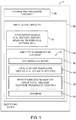
- Electronic devices such as device 10 of FIG. 1 may be provided with wireless communications circuitry.
- the wireless communications circuitry may be used to support long-range wireless communications such as communications in cellular telephone bands.
- long-range wireless communications such as communications in cellular telephone bands.
- Examples of long-range (cellular telephone) bands that may be handled by device 10 include the 800 MHz band, the 850 MHz band, the 900 MHz band, the 1800 MHz band, the 1900 MHz band, the 2100 MHz band, the 700 MHz band, and other bands.
- the long-range bands used by device 10 may include the so-called LTE (Long Term Evolution) bands.
- the LTE bands are numbered (e.g., 1, 2, 3, etc.) and are sometimes referred to as E-UTRA operating bands.
- Long-range signals such as signals associated with satellite navigation bands may be received by the wireless communications circuitry of device 10.
- device 10 may use wireless circuitry to receive signals in the 1575 MHz band associated with Global Positioning System (GPS) communications.
- GPS Global Positioning System
- Short-range wireless communications may also be supported by the wireless circuitry of device 10.
- device 10 may include wireless circuitry for handling local area network links such as WiFi® links at 2.4 GHz and 5 GHz, Bluetooth® links at 2.4 GHz, etc.
- device 10 may include storage and processing circuitry 28.
- Storage and processing circuitry 28 may include storage such as hard disk drive storage, nonvolatile memory (e.g., flash memory or other electrically-programmable-read-only memory configured to form a solid state drive), volatile memory (e.g., static or dynamic random-access-memory), etc.
- Processing circuitry in storage and processing circuitry 28 may be used to control the operation of device 10. This processing circuitry may be based on one or more microprocessors, microcontrollers, digital signal processors, application specific integrated circuits, etc.
- Storage and processing circuitry 28 may be used to run software on device 10, such as internet browsing applications, voice-over-internet-protocol (VOIP) telephone call applications, email applications, media playback applications, operating system functions, functions related to communications band selection during radio-frequency transmission and reception operations, etc.
- VOIP voice-over-internet-protocol
- storage and processing circuitry 28 may be used in implementing communications protocols.
- Communications protocols that may be implemented using storage and processing circuitry 28 include internet protocols, wireless local area network protocols (e.g., IEEE 802.11 protocols -- sometimes referred to as WiFi®), protocols for other short-range wireless communications links such as the Bluetooth® protocol, cellular telephone protocols, MIMO (multiple input multiple output) protocols, antenna diversity protocols, etc.
- Wireless communications operations such as communications band selection operations may be controlled using software stored and running on device 10 (i.e., stored and running on storage and processing circuitry 28 and/or input-output circuitry 30).
- Input-output circuitry 30 may include input-output devices 32.
- Input-output devices 32 may be used to allow data to be supplied to device 10 and to allow data to be provided from device 10 to external devices.
- Input-output devices 32 may include user interface devices, data port devices, and other input-output components.
- input-output devices may include touch screens, displays without touch sensor capabilities, buttons, joysticks, click wheels, scrolling wheels, touch pads, key pads, keyboards, microphones, cameras, buttons, speakers, status indicators, light sources, audio jacks and other audio port components, digital data port devices, light sensors, motion sensors (accelerometers), capacitance sensors, proximity sensors, etc.
- Input-output circuitry 30 may include wireless communications circuitry 34 for communicating wirelessly with external equipment.
- Wireless communications circuitry 34 may include radio-frequency (RF) transceiver circuitry formed from one or more integrated circuits, power amplifier circuitry, low-noise input amplifiers, passive RF components, one or more antennas, transmission lines, and other circuitry for handling RF wireless signals.
- RF radio-frequency
- Wireless signals can also be sent using light (e.g., using infrared communications).
- Wireless communications circuitry 34 may include radio-frequency transceiver circuitry 90 for handling various radio-frequency communications bands.
- circuitry 34 may include transceiver circuitry 36, 38, and 42.
- Transceiver circuitry 36 may handle 2.4 GHz and 5 GHz bands for WiFi® (IEEE 802.11) communications and may handle the 2.4 GHz Bluetooth® communications band.
- Circuitry 34 may use cellular telephone transceiver circuitry 38 for handling wireless communications in cellular telephone bands such as at 850 MHz, 900 MHz, 1800 MHz, 1900 MHz, and 2100 MHz and/or the LTE bands and other bands (as examples).
- Circuitry 38 may handle voice data and non-voice data.
- Wireless communications circuitry 34 may include global positioning system (GPS) receiver equipment such as GPS receiver circuitry 42 for receiving GPS signals at 1575 MHz or for handling other satellite positioning data.
- GPS global positioning system
- WiFi® and Bluetooth® links and other short-range wireless links wireless signals are typically used to convey data over tens or hundreds of feet.
- cellular telephone links and other long-range links wireless signals are typically used to convey data over thousands of feet or miles.
- Wireless communications circuitry 34 may include one or more antennas 40.
- Antennas 40 may be formed using any suitable antenna types.
- antennas 40 may include antennas with resonating elements that are formed from loop antenna structure, patch antenna structures, inverted-F antenna structures, slot antenna structures, planar inverted-F antenna structures, helical antenna structures, hybrids of these designs, etc.
- Different types of antennas may be used for different bands and combinations of bands. For example, one type of antenna may be used in forming a local wireless link antenna and another type of antenna may be used in forming a remote wireless link antenna.
- Antenna diversity schemes may be implemented in which multiple redundant antennas are used in handling communications for a particular band or bands.
- storage and processing circuitry 28 may select which antenna to use in real time based on signal strength measurements or other data.
- multiple antennas may be used to transmit and receive multiple data streams, thereby enhancing data throughput.
- housing 12 may include plastic walls, metal housing structures, structures formed from carbon-fiber materials or other composites, glass, ceramics, or other suitable materials. Housing 12 may be formed using a single piece of material (e.g., using a unibody configuration) or may be formed from a frame, housing walls, and other individual parts that are assembled to form a completed housing structure. The components of device 10 that are shown in FIG. 1 may be mounted within housing 12. Antenna structures 40 may be mounted within housing 12 and may, if desired, be formed using parts of housing 12. For example, housing 12 may include metal housing sidewalls, peripheral conductive members such as band-shaped members (with or without dielectric gaps), conductive bezels, and other conductive structures that may be used in forming antenna structures 40.
- housing 12 may include metal housing sidewalls, peripheral conductive members such as band-shaped members (with or without dielectric gaps), conductive bezels, and other conductive structures that may be used in forming antenna structures 40.
- antenna structures 40 may be coupled to transceiver circuitry 90 by paths such as paths 45.
- Paths 45 may include transmission line structures such as coaxial cables, microstrip transmission lines, stripline transmission lines, etc.
- Paths 45 may also include impedance matching circuitry, filter circuitry, and switching circuitry. Impedance matching circuitry may be used to ensure that antennas 40 are efficiently coupled to transceiver circuitry 90 in communications bands of interest.
- Filter circuitry may be used to implement frequency-based multiplexing circuits such as diplexers and triplexers.
- Switching circuitry may be used to selectively couple antennas 40 to desired ports of transceiver circuitry 90.
- a switch in one operating mode may be configured to route one of paths 45 to a given antenna and in another operating mode the switch may be configured to route a different one of paths 45 to the given antenna.
- the use of switching circuitry between transceiver circuitry 90 and antennas 40 allows device 10 to support multiple communications bands of interest with a limited number of antennas.
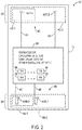
- antennas 40 In a device such as a cellular telephone that has an elongated rectangular outline, it may be desirable to place antennas 40 at one or both ends of the device. As shown in FIG. 2 , for example, some of antennas 40 may be placed in upper end region 42 of housing 12 and some of antennas 40 may be placed in lower end region 44 of housing 12.
- the antenna structures in device 10 may include a single antenna in region 42, a single antenna in region 44, multiple antennas in region 42, multiple antennas in region 44, or may include one or more antennas located elsewhere in housing 12.
- Antenna structures 40 may be formed within some or all of regions such as regions 42 and 44.
- an antenna such as antenna 40T-1 may be located within region 42-1 or an antenna such as antenna 40T-2 may be formed that fills some or all of region 42-1.
- An antenna such as antenna 40B-1 may fill some or all of region 44-2 or an antenna such as antenna 40B-2 may be formed in region 44-1.
- region 44 may contain a first antenna such as antenna 40B-1 and a second antenna such as antenna 40B-2.
- Transceiver circuitry 90 may contain transmitters such as transmitters 48 and receivers such as receivers 50.
- Transmitters 48 and receivers 50 may be implemented using one or more integrated circuits (e.g., cellular telephone communications circuits, wireless local area network communications circuits, circuits for Bluetooth® communications, circuits for receiving satellite navigation system signals, power amplifier circuits for increasing transmitted signal power, low noise amplifier circuits for increasing signal power in received signals, other suitable wireless communications circuits, and combinations of these circuits).
- integrated circuits e.g., cellular telephone communications circuits, wireless local area network communications circuits, circuits for Bluetooth® communications, circuits for receiving satellite navigation system signals, power amplifier circuits for increasing transmitted signal power, low noise amplifier circuits for increasing signal power in received signals, other suitable wireless communications circuits, and combinations of these circuits.
- Device 10 may be a relatively large device (e.g. the lateral dimensions of housing 12 may be tens of centimeters or larger) or may be a relatively compact device such as a handheld device that has a longitudinal dimension along the main axis of housing 12 that is 15 cm or less, 10 cm or less, or 5 cm or less, and that has smaller transverse dimensions.
- the dimensions of housing 12 may be 10 cm or less or 5 cm or less (as examples).
- antennas 40T-1 and 40T-2 in the example of FIG. 2 may be located adjacent to each other within housing 12.
- Other antennas e.g., the antenna structures of region 42 and the antenna structures of region 44 may be separated only by the relatively modest length of device 10.
- switches in paths 45 may have non-linear properties that lead to the generation of second harmonics, third harmonics, and higher-order harmonics when passing radio-frequency signals.
- radio-frequency signals that are generated by transceiver 90 may are transmitted through paths 45 to antennas 40.
- Transmitted signals may, for example, be generated at a frequency f at one of the ports associated with transceiver 90.
- Frequency f may be associated with a cellular telephone band or other frequency of interest.
- Paths 45 may contain a switch such as a transistor-based switch. As the signals at frequency f pass through the switch (and other non-linear circuit elements in paths 45), frequency harmonics may be generated at frequencies such as 2f, 3f, 4f, and higher.
- a signal harmonic at 2f, 3f, 4f, or higher might be transmitted from one antenna (e.g., a cellular telephone antenna) at the same time that signals at frequency f are being transmitted.
- the frequency harmonics at 2f, 3f, and 4f might then be received by another antenna in the device (e.g., a wireless local area network antenna or satellite navigation antenna).
- the received signals at harmonic frequencies of frequency f may cause undesirable interference.
- a received signal at 2f, 3f, or 4f might fall within or near a communications band of one of receivers 50 (e.g., a wireless local area network receiver or satellite navigation system receiver). Left uncorrected, the presence of this type of interference may prevent satisfactory simultaneous operation of the transmitter at frequency f and the receiver operating at 2f, 3f, 4f, or other harmonic.
- Device 10 can reduce or eliminate this type of undesirable interference by including filtering circuitry in paths 45 that blocks harmonics associated with transmitted signals before they reach antennas 40. Because the magnitude of transmitted harmonics is substantially reduced, the magnitude of any harmonics that are received by other antenna and receiver circuitry in device 10 is substantially reduced. By effectively preventing harmonics from being transmitted, the potential for signal interference is eliminated and satisfactory device operation is ensured.
- the filtering circuitry may include a diplexer filter that is used to multiplex low band and high band transmitted signals onto a common transmit path. During signal reception operations, the diplexer demultiplexes received signals based on their frequency.
- the diplexer may include a low pass filter that is coupled to low band transceiver ports through a low band switch.
- the diplexer may also include a high pass filter or a bandpass filter that is coupled to high band transceiver ports through a high band switch.
- harmonics Even if harmonics are generated in the switches, the harmonics will be blocked by the filtering circuitry of the diplexer. For example, consider a low band frequency such as frequency f. As a signal at this frequency passes through the low band switch, harmonic signals at 2f, 3f, and 4f may be generated. By proper configuration of the cutoff frequency of the low pass filter, signal frequency f will fall within the pass band of the low pass filter, but signal frequencies 2f, 3f, and 4f will fall outside of the pass band and will be attenuated.
- receivers 50 in device 10 that operate at or near harmonic frequencies (e.g., 2f, 3f, 4f, and higher) will not be subject to harmonic interference and can operate at the same time as the transmitter operating at frequency f.
- Frequency harmonics generated when transmitting signals from the high band transceiver through the high band switch can likewise be attenuated by the high-frequency attenuation properties of the high-band filter (i.e., when the high-band filter is implemented using a bandpass filter that passes desired high-band frequencies while attenuating harmonics of these desired high-band frequencies).
- a filtering arrangement based on a diplexer scheme of this type may exhibit lower insertion loss than filtering arrangements based on components with higher insertion losses such as notch filters.
- additional filtering circuitry may be used in device 10.
- the filtering circuitry in paths 45 may, include diplexers, triplexers, notch filters, bandpass filters, low pass filters, high pass filters, other filter components, and combinations of filter circuits such as these.
- Filtering components may, for example, be implemented using surface acoustic wave (SAW) or bulk acoustic wave (BAW) devices.
- SAW surface acoustic wave
- BAW bulk acoustic wave
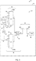
- device 10 may include antennas 40 in housing 12.
- Antennas 40 may be coupled to transceiver circuitry 38 and 46 using paths 45.
- Paths 45 may include switching circuitry 64.
- Antennas 40 may include one or more antennas.
- One or more antennas 40 may, for example, be used for cellular telephone communications bands, one or more antennas 40 may be used for satellite navigation system bands such as the GPS band at 1575 MHz, and one or more antennas 40 may be used for other communications bands of interest (e.g. the IEEE 802.11 bands at 2.4 GHz and 5 GHz or other wireless local area network bands, the Bluetooth® band at 2.4 GHz, etc.).
- the IEEE 802.11 bands at 2.4 GHz and 5 GHz or other wireless local area network bands e.g. the IEEE 802.11 bands at 2.4 GHz and 5 GHz or other wireless local area network bands, the Bluetooth® band at 2.4 GHz, etc.
- one or more antennas such as antenna 40A may be associated with wireless transceiver circuitry such as remote wireless transceiver circuitry 38 (e.g., one or more cellular telephone transceiver circuits) and one or more antennas such as antenna 40B may be associated with wireless transceiver circuitry 46 (e.g., satellite navigation system receiver 42 of FIG. 1 , local wireless transceiver circuits 36 of FIG. 1 such as IEEE 802.11 wireless local area network circuits, Bluetooth® circuits, etc.). Additional antennas may be associated with transceiver circuitry 38 (i.e., antennas in addition to antenna 40A) and additional antennas may be associated with transceiver circuitry 46 (i.e., antennas in addition to antenna 40B), if desired.
- wireless transceiver circuitry such as remote wireless transceiver circuitry 38 (e.g., one or more cellular telephone transceiver circuits) and one or more antennas such as antenna 40B may be associated with wireless transceiver circuitry 46 (e.g
- Transceiver circuitry 38 may include transmitters 48 and receivers 50. There may be, for example, a respective transmitter 48 and a respective receiver 50 associated with each of a plurality of cellular telephone communications bands.
- LTE Band 13 LTE Band 13
- transmitters 48 e.g., transmitter TX of FIG. 3
- receivers 50 e.g., receiver RX of FIG. 3
- paths 45 may include power amplifiers such as power amplifier 52.
- paths 45 may include low noise amplifiers (LNAs) such as low noise amplifier 60.
- LNAs low noise amplifiers
- Amplifiers such as amplifiers 52 and 60 may be implemented using discrete components, using circuitry that is part of a transceiver integrated circuit, etc.
- Switching circuitry 64 may include multiple switches each of which is associated with a respective frequency range.
- switching circuitry 64 includes first switch 64LB and second switch 64HB.
- the states of switches 64LB and 64HB i.e., which terminals are connected to each other in the switches) may be controlled by using storage and processing circuitry 28 to apply control signals to control terminals 62.
- Switch 64LB may be used to handle radio-frequency signals with lower frequencies than switch 64HB. With this type of arrangement, switch 64LB may sometimes be referred to as a low band switch and switch 64HB may sometimes be referred to as a high band switch.
- Switches 64LB and 64HB preferably have a sufficient number of terminals (switch ports) to allow all desired transmitters 48 and receivers 50 to be coupled to antennas 40.
- switches 64LB and 64HB may be SP4T (single pole four throw) or SP5T (single pole five throw) switches (as an example). Switches with more terminals or fewer terminals may be used if desired.
- Each switch has one terminal T' that is coupled to diplexer 68 and a plurality of other terminals T that are each coupled to a respective portion of transceiver circuitry 38.
- each transmitter and receiver pair in transceiver circuitry 38 is coupled to a respective terminal T in switch 64LB or 64HB using a component such as diplexer 54. With this type of arrangement, transmit and receive signals for each band of interest are associated with a respective switch terminal T.
- low band switch 64LB has a plurality of terminals T each of which is coupled to a respective transmitter 48 and receiver 50 by a respective path 66 and associated filter circuitry such as diplexer 54.
- transmitter TX may be connected to filter 56 in diplexer 54 and receiver RX may be connected to filter 58 in diplexer 54.
- Filter 56 may be a high pass filter that passes signals in the uplink range of Band 13 and filter 58 may be a low pass filter that passes signals in the downlink range of Band 13.
- Diplexer 54 may be coupled to a given one of terminals T in low band switch 64LB by one of paths 66. Transmitted signals from transmitter TX in the uplink frequency range for Band 13 may be routed to the given terminal T by power amplifier 52 and filter 56 of diplexer 54. Received signals in the downlink frequency range for Band 13 may be routed from the given terminal T to receiver RX by filter 58 and low noise amplifier 60. Other bands (e.g., other LTE bands, GSM bands, etc.) may be handled using their own respective transmitters 48, power amplifiers 52, receivers 50, low noise amplifiers 60, and diplexers 54.
- Other bands e.g., other LTE bands, GSM bands, etc.
- the transceiver circuitry for a first set of the frequency bands handled by transceiver circuitry 38 may be coupled to the terminals T of low band switch 64LB.
- the transceiver circuitry for a second set of the frequency bands handled by transceiver circuitry 38 may be coupled to the terminals T of high band switch 64HB.
- frequencies below about 960 MHz may be handled by low band switch 64LB and frequencies above about 1710 MHz may be handled by high band switch 64HB.
- Other configurations may be used in wireless circuitry 34 if desired. These frequency assignments are merely illustrative.
- Diplexer 68 may have filters FLB and FHB and ports (terminals) PL, PH, and PA. Terminal T' of switch 64LB may be coupled to port PL. Terminal T' of switch 64HB may be coupled to port PH. Port PA of diplexer 68 may be coupled to antenna 40A. Filter FLB may be a low pass filter. Filter FHB may be a high pass filter or a bandpass filter. Diplexer 68 may use filters FLB and FHB to route radio-frequency signals between switching circuitry 64 and antenna 40A according to frequency, while blocking undesired signal harmonics.
- FIG. 4 is a graph showing an illustrative radio-frequency signal transmission characteristic that may be associated with filter FLB.
- filter FLB may be a low pass filter that passes signals with frequencies f below frequency f1.
- the value of f1 may be, for example, 960 MHz or other frequency that is above the frequencies f LB1 ... f LBN of the communications bands that are being transmitted and received via switch 64LB.
- diplexer 68 may exhibit an insertion loss of about 0.3 dB between ports PL and PA (i.e., maximum transmission value T2 of filter FLB may be about 0.3 dB below 100% transmission level T1, as indicated by the gap between 100% transmission curve 70 and transmission curve 72 of filter FLB.
- FIG. 5 is a graph showing an illustrative radio-frequency signal transmission characteristic that may be associated with filter FHB.
- filter FLB may be a high pass filter (see, e.g., curve 76 and curve portion 80-2) or a bandpass filter (see, e.g., curve 76 and curve portion 80-1) that passes signals with frequencies f above frequency f2.
- the value of f2 may be, for example, 1710 MHz or other frequency that is below the frequencies f HB1 ...f HBN of the communications bands that are being transmitted and received via switch 64HB.
- diplexer 68 may exhibit an insertion loss of about 0.3 dB between ports PH and PA.
- the maximum transmission value T2 of filter FHB may be about 0.3 dB below 100% transmission level T1, as indicated by the gap between 100% transmission curve 70 and transmission curve 76 of filter FHB (diplexer 68).
- the insertion losses associated with diplexer 68 may be somewhat higher or lower than the illustrative 0.3 dB insertion loss shown in FIGS. 4 and 5 . Nevertheless, the insertion losses associated with use of a diplexer such as diplexer 68 will generally be significantly less than the insertion losses that would result if other types of filtering circuitry such as notch filters were to be interposed between switching circuitry 64 and antenna 40A.
- Switching circuitry 64 may be implemented using switches 64A and 64B that include gallium arsenide field-effect transistors (FETs), microelectromechanical systems (MEMs) switches, metal-oxide-semiconductor field-effect transistors (MOSFETs), p-i-n diodes, high-electron mobility transistors (HEMTs), pseudomorphic HEMT (PHEMTs), transistors formed on a silicon-on-insulator (SOI) substrate, etc.
- FETs gallium arsenide field-effect transistors
- MEMs microelectromechanical systems
- MOSFETs metal-oxide-semiconductor field-effect transistors
- HEMTs high-electron mobility transistors
- PHEMTs pseudomorphic HEMT
- SOI silicon-on-insulator
- the filters of diplexer 68 can significantly attenuate these harmonics, so that the harmonics are not transmitted through antenna 40A and are therefore not received by antenna 40B. Because antenna 40B does not receive harmonics of any significant magnitude, the receivers associated with transceiver 46 (i.e., wireless local area network receiver circuitry, satellite navigation receiver circuitry, etc.) will operate properly without interference from the operation of transceiver circuitry 38.
- transceiver 46 i.e., wireless local area network receiver circuitry, satellite navigation receiver circuitry, etc.
- harmonics of some of the transmitted LTE bands may fall within IEEE 802.11 (WiFi®) bands at 2.4 GHz and 5 GHz and/or satellite navigation system bands such as the GPS band at 1575 MHz.
- WiFi® IEEE 802.11
- the uplink (transmit) band associated with Band 13 extends from 777 MHz to 787 MHz.
- switch 64LB may generate harmonics such as second harmonics in the frequency range of 1554 MHz to 1574 MHz.
- diplexer 68 If not attenuated by diplexer 68, these second harmonics (particularly the harmonic signals near 1574 MHz) might interfere with the GPS band centered at 1575 MHz (i.e., the GPS receiver coupled to antenna 40A).
- the second harmonics in the frequency range of 1554 MHz to 1574 MHz are attenuated significantly (e.g., by 15 dB or more, by 30 dB or more, etc.).
- low pass filter FLB significantly attenuates signals at frequencies above f1 (e.g., above 960 MHz or other suitable cutoff frequency).
- the third harmonics of LTE bands 1, 3, 4, and 2 may represent a possible source of interference with the IEEE 802.11 wireless local area network band at 5 GHz.
- third harmonics in the vicinity of 5 GHz may be produced.
- curve 76 and, in particular, curve segment 80-1 of FIG. 5 when filter FHB is implemented as a bandpass filter (i.e., when filter FHB passes signals in a frequency range f2 to f3 of about 1710 MHz to 2.25 GHz), signals above 2.25 GHz (i.e., the harmonics in the vicinity of 5 GHz) will be attenuated by filter FHB.
- diplexer 68 prevents transmitted signal harmonics from being transmitted through antenna 40B, these harmonics will not be received by antenna 40A, even when antennas 40A and 40B are located within the same device (e.g., at ends 44 and 42, respectively) and are potentially in close proximity to each other (e.g., 15 cm or less apart, etc.).
- the lower cutoff frequency f2 and upper cutoff frequency f3 of high band filter FHB may be lower or higher to accommodate different transmitted bands.
- filter FHB may be implemented using a high pass filter (i.e., filter with a low frequency cutoff such as frequency f2 of FIG. 5 , but no sharp upper frequency cutoff such as frequency f3 so that curve 76 follows segment 80-2 above f3).
- Low band filter FLB can be implemented using different cutoff frequencies. The use of a 960 MHz cutoff frequency for frequency f1 of FIG. 1 is presented as an example.
- the first set of radio-frequency transmitters includes a cellular telephone transmitter that produces transmitted signals at frequency f and the low pass filter prevents signals at 2f from reaching the antenna.
- the diplexer includes a low pass filter and a bandpass filter.
- the second set of radio-frequency transmitters includes a Long Term Evolution (LTE) cellular telephone transmitter operating in an LTE Band selected from the group of bands including Band 1, Band 3, Band 4, and Band 2, the LTE cellular telephone transmitter produces transmitted signals at a frequency f, and the bandpass filter prevents signals at a frequency of 3f from reaching the antenna.
- LTE Long Term Evolution
- the first set of radio-frequency transmitters includes an additional LTE cellular telephone transmitter operating in LTE Band 13 that produces signals in LTE Band 13 and the low pass filter prevents signals at a second harmonic of the signals in LTE Band 13 from reaching the antenna.
- an electronic device in accordance with an embodiment, includes a first antenna, a receiver that receives signals in at least a first communications band through the first antenna, a second antenna, a radio-frequency transmitter that transmits signals at a frequency f through the second antenna, a diplexer having a first port, a second port, and a third port that is coupled to the second antenna, a first radio-frequency switch that is coupled to the first port, and a second radio-frequency switch that is coupled between the radio-frequency transmitter and the second port, where the diplexer prevents signals at harmonics of the frequency f from reaching the second antenna and from reaching the receiver through the first antenna.
- the receiver is configured to receive Global Positioning System signals at 1575 MHz and the diplexer includes a low-pass filter that prevents signals at a frequency of 2f that are produced in the second radio-frequency switch in response to the transmission of the signals at the frequency f from the radio-frequency transmitter from reaching the second antenna.
- the receiver is configured to receive IEEE 802.11 signals at 5 GHz and the diplexer includes a bandpass filter that prevents signals at a frequency of 3f that are produced in the second radio-frequency switch in response to the transmission of the signals at the frequency f from the radio-frequency transmitter from reaching the second antenna.
- the diplexer includes a low pass filter and a high pass filter.
- the diplexer includes a low pass filter and a bandpass filter.
- the radio-frequency transmitter includes a cellular telephone transmitter that produces transmitted signals at frequency f and the low pass filter prevents signals at 2f from reaching the antenna.
- the receiver includes satellite receiver circuitry that receives satellite navigation signals through the first antenna.
- the radio-frequency transmitter includes a Long Term Evolution (LTE) cellular telephone transmitter operating in LTE Band 13.
- LTE Long Term Evolution
- wireless circuitry includes a set of radio-frequency transmitters that operate in a set of communications bands, a switch having a plurality of switch terminals each of which is coupled to a respective one of the radio-frequency transmitters in the set of radio-frequency transmitters and having an additional terminal to which a selected one of the plurality of switch terminals is connected, an antenna, and a diplexer having a first port that is coupled to the additional terminal of the switch, a second port, and a third port that is coupled to the antenna.
- the wireless circuitry also includes satellite receiver circuitry that receives satellite navigation signals through the antenna.
- the set of radio-frequency transmitters includes a first set of radio-frequency transmitters and the set of communications bands includes a first set of communications band and the wireless circuitry also includes a second set of radio-frequency transmitters that operate in a second set of communications bands.
- the switch includes a first switch
- the wireless circuitry also includes a second switch having a plurality of switch terminals each of which is coupled to a respective one of the radio-frequency transmitters in the second set of radio-frequency transmitters and having an additional terminal to which a selected one of the plurality of second switch terminals is connected, and the second port of the diplexer is coupled to the additional terminal of the second switch.
Landscapes
- Engineering & Computer Science (AREA)
- Computer Networks & Wireless Communication (AREA)
- Signal Processing (AREA)
- Transceivers (AREA)
- Noise Elimination (AREA)
- Transmitters (AREA)
Description
- The invention relates generally to wireless communications circuitry, and more particularly, to circuitry in wireless electronic devices that reduces interference from frequency harmonics.
- Electronic devices such as computers and cellular telephones are often provided with wireless communications capabilities. For example, electronic devices may use long-range wireless communications circuitry such as cellular telephone circuitry. Global Positioning System (GPS) receiver circuitry and other satellite receiver circuitry may be used to receive satellite navigation signals. Local wireless links may be used to support local area network communications such as IEEE 802.11 communications at 2.4 GHz and 5 GHz. Local links may also be used to handle Bluetooth® communications at 2.4 GHz.
- It is often desirable for a device to support multiple bands. For example, users of a cellular telephone may desire to communicate with cellular telephone towers using one or more different cellular telephone bands and may desire to communicate with local area network equipment using wireless local area network (WLAN) communications bands.
- When supporting multiple bands, it is sometimes desirable to use configurable switching circuitry to route signals. In a device having a transceiver with numerous transceiver ports, for example, a switch may be used to selectively couple a selected one of the transceiver ports to an antenna. This type of configuration allows the device to be configured in different ways, depending on the desired band of operation. If, for example, it is desired to use a first communications band, the switch may be placed in a first state that couples a first transceiver port to the antenna. When it is desired to use a second communications band, the switch may be placed in a second state that couples a second transceiver port to the antenna.
- Radio-frequency switches may be based on components such as transistors that exhibit non-linear behavior. As a result, undesired frequency harmonics may be generated when radio-frequency signals are transmitted through a switch. For example, second harmonics, third harmonics, and higher-order harmonics of transmitted radio-frequency signals may be generated. If care is not taken, these harmonic signals may interfere with the operation of receiver circuitry in the device. For example, harmonics that are generated during transmission of cellular telephone signals may interfere with proper operation of a satellite navigation receiver or wireless local area network receiver.
-
EP 1 551 080 A1 discloses an antenna device and the pre-characterising portion of the appended claims is based on this document.US 2004/0224643 discloses a wireless multimode front end module. - It would therefore be desirable to be able provide improved circuitry for routing signals between radio-frequency transceiver ports and antenna structures in a wireless electronic device.
- An electronic device may be provided with wireless communications circuitry as claimed in the appended claims. The wireless communications circuitry may include radio-frequency transceiver circuitry for handling wireless communications. The radio-frequency transceiver may have multiple transmitters and multiple receivers. Antenna structures may be used to transmit and receive signals.
- The antenna structures may be coupled to transmitters and receivers in the radio-frequency transceiver circuitry. Switching circuitry such as first and second radio-frequency switches are used to support multiple communications bands of interest. The first and second radio-frequency switches may be configured in real time to switch desired frequencies into use.
- A set of low band transmitters and receivers may be associated with the first switch and a set of high band transmitters and receivers may be associated with the second switch. As transmitted signals at frequency f pass through the switches, harmonics at 2f, 3f, and other integral multiples of the transmitted signals may be produced.
- A diplexer is interposed between the first and second switches and the antenna structures. The diplexer has a first port that is coupled to the first radio-frequency switch, a second port that is coupled to the second radio-frequency switch, and a third port that is coupled to one or more antennas in the antenna structures.
- The diplexer may include a low band filter associated with the low band transmitters and receivers and a high band filter associated with the high band transmitters and receivers. The low band filter may be a low pass filter that is coupled between the first switch and the antenna structures. The low pass filter may prevent transmitted signal harmonics that exit the first switch from reaching the antenna structures. The diplexer may include high band and low band filters that exhibit high degrees of linearity such as filters implemented on ceramic substrates. Highly linear filters such as filters with ceramic substrates may have a reduced tendency to produce undesired harmonics relative to other filter designs.
- The high band filter may be a high pass filter or a band pass filter. When implemented using a bandpass filter, the high band filter may prevent transmitted signal harmonics that exit the second switch from reaching the antenna structures.
- Further features of the invention, its nature and various advantages will be more apparent from the accompanying drawings and the following detailed description of the preferred embodiments.
-
-
FIG. 1 is a schematic diagram of an illustrative electronic device with wireless communications circuitry in accordance with an embodiment of the present invention. -
FIG. 2 is a diagram showing how radio-frequency transceiver circuitry may be coupled to one or more antennas within an electronic device of the type shown inFIG. 1 in accordance with an embodiment of the present invention. -
FIG. 3 is a circuit diagram of illustrative wireless communications circuitry of the type that may be used in handling wireless communications in the electronic device ofFIG. 1 in accordance with an embodiment of the present invention. -
FIG. 4 is a graph of radio-frequency signal transmission as a function of operating frequency for an illustrative low band filter that may be used in a diplexer within the wireless circuitry ofFIG. 3 in accordance with an embodiment of the present invention. -
FIG. 5 is a graph of radio-frequency signal transmission as a function of operating frequency for an illustrative high band filter that may be used in a diplexer within the wireless circuitry ofFIG. 3 in accordance with an embodiment of the present invention. - Electronic devices such as
device 10 ofFIG. 1 may be provided with wireless communications circuitry. The wireless communications circuitry may be used to support long-range wireless communications such as communications in cellular telephone bands. Examples of long-range (cellular telephone) bands that may be handled bydevice 10 include the 800 MHz band, the 850 MHz band, the 900 MHz band, the 1800 MHz band, the 1900 MHz band, the 2100 MHz band, the 700 MHz band, and other bands. The long-range bands used bydevice 10 may include the so-called LTE (Long Term Evolution) bands. The LTE bands are numbered (e.g., 1, 2, 3, etc.) and are sometimes referred to as E-UTRA operating bands. Long-range signals such as signals associated with satellite navigation bands may be received by the wireless communications circuitry ofdevice 10. For example,device 10 may use wireless circuitry to receive signals in the 1575 MHz band associated with Global Positioning System (GPS) communications. Short-range wireless communications may also be supported by the wireless circuitry ofdevice 10. For example,device 10 may include wireless circuitry for handling local area network links such as WiFi® links at 2.4 GHz and 5 GHz, Bluetooth® links at 2.4 GHz, etc. - As shown in
FIG. 1 ,device 10 may include storage andprocessing circuitry 28. Storage andprocessing circuitry 28 may include storage such as hard disk drive storage, nonvolatile memory (e.g., flash memory or other electrically-programmable-read-only memory configured to form a solid state drive), volatile memory (e.g., static or dynamic random-access-memory), etc. Processing circuitry in storage andprocessing circuitry 28 may be used to control the operation ofdevice 10. This processing circuitry may be based on one or more microprocessors, microcontrollers, digital signal processors, application specific integrated circuits, etc. - Storage and
processing circuitry 28 may be used to run software ondevice 10, such as internet browsing applications, voice-over-internet-protocol (VOIP) telephone call applications, email applications, media playback applications, operating system functions, functions related to communications band selection during radio-frequency transmission and reception operations, etc. To support interactions with external equipment, storage andprocessing circuitry 28 may be used in implementing communications protocols. Communications protocols that may be implemented using storage andprocessing circuitry 28 include internet protocols, wireless local area network protocols (e.g., IEEE 802.11 protocols -- sometimes referred to as WiFi®), protocols for other short-range wireless communications links such as the Bluetooth® protocol, cellular telephone protocols, MIMO (multiple input multiple output) protocols, antenna diversity protocols, etc. Wireless communications operations such as communications band selection operations may be controlled using software stored and running on device 10 (i.e., stored and running on storage andprocessing circuitry 28 and/or input-output circuitry 30). - Input-
output circuitry 30 may include input-output devices 32. Input-output devices 32 may be used to allow data to be supplied todevice 10 and to allow data to be provided fromdevice 10 to external devices. Input-output devices 32 may include user interface devices, data port devices, and other input-output components. For example, input-output devices may include touch screens, displays without touch sensor capabilities, buttons, joysticks, click wheels, scrolling wheels, touch pads, key pads, keyboards, microphones, cameras, buttons, speakers, status indicators, light sources, audio jacks and other audio port components, digital data port devices, light sensors, motion sensors (accelerometers), capacitance sensors, proximity sensors, etc. - Input-
output circuitry 30 may includewireless communications circuitry 34 for communicating wirelessly with external equipment.Wireless communications circuitry 34 may include radio-frequency (RF) transceiver circuitry formed from one or more integrated circuits, power amplifier circuitry, low-noise input amplifiers, passive RF components, one or more antennas, transmission lines, and other circuitry for handling RF wireless signals. Wireless signals can also be sent using light (e.g., using infrared communications). -
Wireless communications circuitry 34 may include radio-frequency transceiver circuitry 90 for handling various radio-frequency communications bands. For example,circuitry 34 may includetransceiver circuitry Transceiver circuitry 36 may handle 2.4 GHz and 5 GHz bands for WiFi® (IEEE 802.11) communications and may handle the 2.4 GHz Bluetooth® communications band.Circuitry 34 may use cellulartelephone transceiver circuitry 38 for handling wireless communications in cellular telephone bands such as at 850 MHz, 900 MHz, 1800 MHz, 1900 MHz, and 2100 MHz and/or the LTE bands and other bands (as examples).Circuitry 38 may handle voice data and non-voice data. -
Wireless communications circuitry 34 may include global positioning system (GPS) receiver equipment such asGPS receiver circuitry 42 for receiving GPS signals at 1575 MHz or for handling other satellite positioning data. In WiFi® and Bluetooth® links and other short-range wireless links, wireless signals are typically used to convey data over tens or hundreds of feet. In cellular telephone links and other long-range links, wireless signals are typically used to convey data over thousands of feet or miles. -
Wireless communications circuitry 34 may include one ormore antennas 40.Antennas 40 may be formed using any suitable antenna types. For example,antennas 40 may include antennas with resonating elements that are formed from loop antenna structure, patch antenna structures, inverted-F antenna structures, slot antenna structures, planar inverted-F antenna structures, helical antenna structures, hybrids of these designs, etc. Different types of antennas may be used for different bands and combinations of bands. For example, one type of antenna may be used in forming a local wireless link antenna and another type of antenna may be used in forming a remote wireless link antenna. - Antenna diversity schemes may be implemented in which multiple redundant antennas are used in handling communications for a particular band or bands. In an antenna diversity scheme, storage and
processing circuitry 28 may select which antenna to use in real time based on signal strength measurements or other data. In multiple-input-multiple-output (MIMO) schemes, multiple antennas may be used to transmit and receive multiple data streams, thereby enhancing data throughput. - Illustrative locations in which
antennas 40 may be formed indevice 10 are shown inFIG. 2 . As shown inFIG. 2 ,electronic device 10 may have a housing such ashousing 12.Housing 12 may include plastic walls, metal housing structures, structures formed from carbon-fiber materials or other composites, glass, ceramics, or other suitable materials.Housing 12 may be formed using a single piece of material (e.g., using a unibody configuration) or may be formed from a frame, housing walls, and other individual parts that are assembled to form a completed housing structure. The components ofdevice 10 that are shown inFIG. 1 may be mounted withinhousing 12.Antenna structures 40 may be mounted withinhousing 12 and may, if desired, be formed using parts ofhousing 12. For example,housing 12 may include metal housing sidewalls, peripheral conductive members such as band-shaped members (with or without dielectric gaps), conductive bezels, and other conductive structures that may be used in formingantenna structures 40. - As shown in
FIG. 2 ,antenna structures 40 may be coupled totransceiver circuitry 90 by paths such aspaths 45.Paths 45 may include transmission line structures such as coaxial cables, microstrip transmission lines, stripline transmission lines, etc.Paths 45 may also include impedance matching circuitry, filter circuitry, and switching circuitry. Impedance matching circuitry may be used to ensure thatantennas 40 are efficiently coupled totransceiver circuitry 90 in communications bands of interest. Filter circuitry may be used to implement frequency-based multiplexing circuits such as diplexers and triplexers. Switching circuitry may be used to selectively coupleantennas 40 to desired ports oftransceiver circuitry 90. For example, in one operating mode a switch may be configured to route one ofpaths 45 to a given antenna and in another operating mode the switch may be configured to route a different one ofpaths 45 to the given antenna. The use of switching circuitry betweentransceiver circuitry 90 andantennas 40 allowsdevice 10 to support multiple communications bands of interest with a limited number of antennas. - In a device such as a cellular telephone that has an elongated rectangular outline, it may be desirable to place
antennas 40 at one or both ends of the device. As shown inFIG. 2 , for example, some ofantennas 40 may be placed inupper end region 42 ofhousing 12 and some ofantennas 40 may be placed in lower end region 44 ofhousing 12. The antenna structures indevice 10 may include a single antenna inregion 42, a single antenna in region 44, multiple antennas inregion 42, multiple antennas in region 44, or may include one or more antennas located elsewhere inhousing 12. -
Antenna structures 40 may be formed within some or all of regions such asregions 42 and 44. For example, an antenna such asantenna 40T-1 may be located within region 42-1 or an antenna such asantenna 40T-2 may be formed that fills some or all of region 42-1. An antenna such as antenna 40B-1 may fill some or all of region 44-2 or an antenna such as antenna 40B-2 may be formed in region 44-1. These types of arrangements need not be mutually exclusive. For example, region 44 may contain a first antenna such as antenna 40B-1 and a second antenna such as antenna 40B-2. -
Transceiver circuitry 90 may contain transmitters such astransmitters 48 and receivers such asreceivers 50.Transmitters 48 andreceivers 50 may be implemented using one or more integrated circuits (e.g., cellular telephone communications circuits, wireless local area network communications circuits, circuits for Bluetooth® communications, circuits for receiving satellite navigation system signals, power amplifier circuits for increasing transmitted signal power, low noise amplifier circuits for increasing signal power in received signals, other suitable wireless communications circuits, and combinations of these circuits). -
Device 10 may be a relatively large device (e.g. the lateral dimensions ofhousing 12 may be tens of centimeters or larger) or may be a relatively compact device such as a handheld device that has a longitudinal dimension along the main axis ofhousing 12 that is 15 cm or less, 10 cm or less, or 5 cm or less, and that has smaller transverse dimensions. In miniature devices such as wrist-mounted, pendant, and clip-mounted devices, the dimensions ofhousing 12 may be 10 cm or less or 5 cm or less (as examples). - Particularly in housings for
device 10 that are compact, it may be difficult or impossible to widely separate various antennas from each other. For example, some antennas (e.g.,antennas 40T-1 and 40T-2 in the example ofFIG. 2 ) may be located adjacent to each other withinhousing 12. Other antennas (e.g., the antenna structures ofregion 42 and the antenna structures of region 44) may be separated only by the relatively modest length ofdevice 10. - Due to the close proximity of the antennas within
device 10 in at least some device configurations, there may be a potential for interference between bands. This potential for interference may be exacerbated by the presence of the circuitry inpaths 45, which may generate undesirable frequency harmonics. For example, switches inpaths 45 may have non-linear properties that lead to the generation of second harmonics, third harmonics, and higher-order harmonics when passing radio-frequency signals. - During data transmission operations, radio-frequency signals that are generated by
transceiver 90 may are transmitted throughpaths 45 toantennas 40. Transmitted signals may, for example, be generated at a frequency f at one of the ports associated withtransceiver 90. Frequency f may be associated with a cellular telephone band or other frequency of interest.Paths 45 may contain a switch such as a transistor-based switch. As the signals at frequency f pass through the switch (and other non-linear circuit elements in paths 45), frequency harmonics may be generated at frequencies such as 2f, 3f, 4f, and higher. In this situation, a signal harmonic at 2f, 3f, 4f, or higher might be transmitted from one antenna (e.g., a cellular telephone antenna) at the same time that signals at frequency f are being transmitted. The frequency harmonics at 2f, 3f, and 4f might then be received by another antenna in the device (e.g., a wireless local area network antenna or satellite navigation antenna). If care is not taken, the received signals at harmonic frequencies of frequency f may cause undesirable interference. For example, a received signal at 2f, 3f, or 4f might fall within or near a communications band of one of receivers 50 (e.g., a wireless local area network receiver or satellite navigation system receiver). Left uncorrected, the presence of this type of interference may prevent satisfactory simultaneous operation of the transmitter at frequency f and the receiver operating at 2f, 3f, 4f, or other harmonic. -
Device 10 can reduce or eliminate this type of undesirable interference by including filtering circuitry inpaths 45 that blocks harmonics associated with transmitted signals before they reachantennas 40. Because the magnitude of transmitted harmonics is substantially reduced, the magnitude of any harmonics that are received by other antenna and receiver circuitry indevice 10 is substantially reduced. By effectively preventing harmonics from being transmitted, the potential for signal interference is eliminated and satisfactory device operation is ensured. - The filtering circuitry may include a diplexer filter that is used to multiplex low band and high band transmitted signals onto a common transmit path. During signal reception operations, the diplexer demultiplexes received signals based on their frequency. The diplexer may include a low pass filter that is coupled to low band transceiver ports through a low band switch. The diplexer may also include a high pass filter or a bandpass filter that is coupled to high band transceiver ports through a high band switch.
- Even if harmonics are generated in the switches, the harmonics will be blocked by the filtering circuitry of the diplexer. For example, consider a low band frequency such as frequency f. As a signal at this frequency passes through the low band switch, harmonic signals at 2f, 3f, and 4f may be generated. By proper configuration of the cutoff frequency of the low pass filter, signal frequency f will fall within the pass band of the low pass filter, but signal frequencies 2f, 3f, and 4f will fall outside of the pass band and will be attenuated. Because the low pass filter blocks undesired harmonic frequencies,
receivers 50 indevice 10 that operate at or near harmonic frequencies (e.g., 2f, 3f, 4f, and higher) will not be subject to harmonic interference and can operate at the same time as the transmitter operating at frequency f. Frequency harmonics generated when transmitting signals from the high band transceiver through the high band switch can likewise be attenuated by the high-frequency attenuation properties of the high-band filter (i.e., when the high-band filter is implemented using a bandpass filter that passes desired high-band frequencies while attenuating harmonics of these desired high-band frequencies). - A filtering arrangement based on a diplexer scheme of this type may exhibit lower insertion loss than filtering arrangements based on components with higher insertion losses such as notch filters. If desired, additional filtering circuitry may be used in
device 10. In general, the filtering circuitry inpaths 45 may, include diplexers, triplexers, notch filters, bandpass filters, low pass filters, high pass filters, other filter components, and combinations of filter circuits such as these. Filtering components may, for example, be implemented using surface acoustic wave (SAW) or bulk acoustic wave (BAW) devices. - An illustrative configuration that may be used for
wireless communications circuitry 34 is shown inFIG. 3 . As shown inFIG. 3 ,device 10 may includeantennas 40 inhousing 12.Antennas 40 may be coupled totransceiver circuitry paths 45.Paths 45 may include switching circuitry 64. -
Antennas 40 may include one or more antennas. One ormore antennas 40 may, for example, be used for cellular telephone communications bands, one ormore antennas 40 may be used for satellite navigation system bands such as the GPS band at 1575 MHz, and one ormore antennas 40 may be used for other communications bands of interest (e.g. the IEEE 802.11 bands at 2.4 GHz and 5 GHz or other wireless local area network bands, the Bluetooth® band at 2.4 GHz, etc.). In a configuration of the type shown in the example ofFIG. 3 , one or more antennas such as antenna 40A may be associated with wireless transceiver circuitry such as remote wireless transceiver circuitry 38 (e.g., one or more cellular telephone transceiver circuits) and one or more antennas such as antenna 40B may be associated with wireless transceiver circuitry 46 (e.g., satellitenavigation system receiver 42 ofFIG. 1 , localwireless transceiver circuits 36 ofFIG. 1 such as IEEE 802.11 wireless local area network circuits, Bluetooth® circuits, etc.). Additional antennas may be associated with transceiver circuitry 38 (i.e., antennas in addition to antenna 40A) and additional antennas may be associated with transceiver circuitry 46 (i.e., antennas in addition to antenna 40B), if desired. -
Transceiver circuitry 38 may includetransmitters 48 andreceivers 50. There may be, for example, arespective transmitter 48 and arespective receiver 50 associated with each of a plurality of cellular telephone communications bands. Consider, as an example, LTE Band 13. To support communications in E-UTRA (LTE) Band 13, one of transmitters 48 (e.g., transmitter TX ofFIG. 3 ) may transmit radio-frequency signals in the uplink frequency range of 777 MHz to 787 MHz and one of receivers 50 (e.g., receiver RX ofFIG. 3 ) may receive radio-frequency signals in the downlink frequency range of 746 MHz to 756 MHz. To increase transmit power before transmitted radio-frequency signals reachantennas 40,paths 45 may include power amplifiers such aspower amplifier 52. To increase the strength of signals that have been received fromantennas 40,paths 45 may include low noise amplifiers (LNAs) such aslow noise amplifier 60. Amplifiers such asamplifiers - Switching circuitry 64 may include multiple switches each of which is associated with a respective frequency range. In the example of
FIG. 3 , switching circuitry 64 includes first switch 64LB and second switch 64HB. The states of switches 64LB and 64HB (i.e., which terminals are connected to each other in the switches) may be controlled by using storage andprocessing circuitry 28 to apply control signals to controlterminals 62. Switch 64LB may be used to handle radio-frequency signals with lower frequencies than switch 64HB. With this type of arrangement, switch 64LB may sometimes be referred to as a low band switch and switch 64HB may sometimes be referred to as a high band switch. - Switches 64LB and 64HB preferably have a sufficient number of terminals (switch ports) to allow all desired
transmitters 48 andreceivers 50 to be coupled toantennas 40. In a typical configuration, switches 64LB and 64HB may be SP4T (single pole four throw) or SP5T (single pole five throw) switches (as an example). Switches with more terminals or fewer terminals may be used if desired. - Each switch has one terminal T' that is coupled to diplexer 68 and a plurality of other terminals T that are each coupled to a respective portion of
transceiver circuitry 38. In a typical configuration, each transmitter and receiver pair intransceiver circuitry 38 is coupled to a respective terminal T in switch 64LB or 64HB using a component such asdiplexer 54. With this type of arrangement, transmit and receive signals for each band of interest are associated with a respective switch terminal T. - In the example of
FIG. 3 , low band switch 64LB has a plurality of terminals T each of which is coupled to arespective transmitter 48 andreceiver 50 by a respective path 66 and associated filter circuitry such asdiplexer 54. For example, transmitter TX may be connected to filter 56 indiplexer 54 and receiver RX may be connected to filter 58 indiplexer 54. Filter 56 may be a high pass filter that passes signals in the uplink range of Band 13 andfilter 58 may be a low pass filter that passes signals in the downlink range of Band 13. -
Diplexer 54 may be coupled to a given one of terminals T in low band switch 64LB by one of paths 66. Transmitted signals from transmitter TX in the uplink frequency range for Band 13 may be routed to the given terminal T bypower amplifier 52 and filter 56 ofdiplexer 54. Received signals in the downlink frequency range for Band 13 may be routed from the given terminal T to receiver RX byfilter 58 andlow noise amplifier 60. Other bands (e.g., other LTE bands, GSM bands, etc.) may be handled using their ownrespective transmitters 48,power amplifiers 52,receivers 50,low noise amplifiers 60, anddiplexers 54. - The transceiver circuitry for a first set of the frequency bands handled by transceiver circuitry 38 (e.g., the lower frequency bands) may be coupled to the terminals T of low band switch 64LB. The transceiver circuitry for a second set of the frequency bands handled by transceiver circuitry 38 (e.g., the higher frequency bands) may be coupled to the terminals T of high band switch 64HB. With one suitable arrangement, frequencies below about 960 MHz may be handled by low band switch 64LB and frequencies above about 1710 MHz may be handled by high band switch 64HB. Other configurations may be used in
wireless circuitry 34 if desired. These frequency assignments are merely illustrative. - Diplexer 68 may have filters FLB and FHB and ports (terminals) PL, PH, and PA. Terminal T' of switch 64LB may be coupled to port PL. Terminal T' of switch 64HB may be coupled to port PH. Port PA of diplexer 68 may be coupled to antenna 40A. Filter FLB may be a low pass filter. Filter FHB may be a high pass filter or a bandpass filter. Diplexer 68 may use filters FLB and FHB to route radio-frequency signals between switching circuitry 64 and antenna 40A according to frequency, while blocking undesired signal harmonics.
-
FIG. 4 is a graph showing an illustrative radio-frequency signal transmission characteristic that may be associated with filter FLB. As shown inFIG. 4 , filter FLB may be a low pass filter that passes signals with frequencies f below frequency f1. The value of f1 may be, for example, 960 MHz or other frequency that is above the frequencies fLB1... fLBN of the communications bands that are being transmitted and received via switch 64LB. Using low pass filter FLB, diplexer 68 may exhibit an insertion loss of about 0.3 dB between ports PL and PA (i.e., maximum transmission value T2 of filter FLB may be about 0.3 dB below 100% transmission level T1, as indicated by the gap between 100% transmission curve 70 andtransmission curve 72 of filter FLB. -
FIG. 5 is a graph showing an illustrative radio-frequency signal transmission characteristic that may be associated with filter FHB. As shown inFIG. 5 , filter FLB may be a high pass filter (see, e.g., curve 76 and curve portion 80-2) or a bandpass filter (see, e.g., curve 76 and curve portion 80-1) that passes signals with frequencies f above frequency f2. The value of f2 may be, for example, 1710 MHz or other frequency that is below the frequencies fHB1...fHBN of the communications bands that are being transmitted and received via switch 64HB. Using high pass filter (or bandpass filter) FLB, diplexer 68 may exhibit an insertion loss of about 0.3 dB between ports PH and PA. As shown inFIG. 5 , for example, the maximum transmission value T2 of filter FHB may be about 0.3 dB below 100% transmission level T1, as indicated by the gap between 100% transmission curve 70 and transmission curve 76 of filter FHB (diplexer 68). The insertion losses associated with diplexer 68 may be somewhat higher or lower than the illustrative 0.3 dB insertion loss shown inFIGS. 4 and5 . Nevertheless, the insertion losses associated with use of a diplexer such as diplexer 68 will generally be significantly less than the insertion losses that would result if other types of filtering circuitry such as notch filters were to be interposed between switching circuitry 64 and antenna 40A. - Switching circuitry 64 may be implemented using switches 64A and 64B that include gallium arsenide field-effect transistors (FETs), microelectromechanical systems (MEMs) switches, metal-oxide-semiconductor field-effect transistors (MOSFETs), p-i-n diodes, high-electron mobility transistors (HEMTs), pseudomorphic HEMT (PHEMTs), transistors formed on a silicon-on-insulator (SOI) substrate, etc. When radio-frequency signals are transmitted from
transmitters 48 to antenna 40A, the transmitted signals pass through switching circuitry 64. Nonlinearities in the behavior of switching circuitry 64 may generate harmonics at terminals T' (i.e., at the outputs of the switches). The filters of diplexer 68 can significantly attenuate these harmonics, so that the harmonics are not transmitted through antenna 40A and are therefore not received by antenna 40B. Because antenna 40B does not receive harmonics of any significant magnitude, the receivers associated with transceiver 46 (i.e., wireless local area network receiver circuitry, satellite navigation receiver circuitry, etc.) will operate properly without interference from the operation oftransceiver circuitry 38. - Consider, as an example, a situation in which the communications bands that pass through low band switch 64LB and low pass filter FLB (i.e., bands 74 at frequencies fLB1...fLBN of
FIG. 4 ) are associated with LTE bands such as some or all of Bands 5, 8, 17, 13, and 20 (and, if desired, other LTE bands and/or other cellular telephone bands), whereas the communications bands that pass through high band switch 64HB and high pass filter (or bandpass filter) HLB (i.e.,bands 78 at frequencies fHB1...fHBN ofFIG. 5 ) are associated with LTE bands such as some or all ofBands 4, 2, 7, 1, 3, and 40 (and, if desired, other LTE bands and/or other cellular telephone bands). In a configuration of this type, harmonics of some of the transmitted LTE bands may fall within IEEE 802.11 (WiFi®) bands at 2.4 GHz and 5 GHz and/or satellite navigation system bands such as the GPS band at 1575 MHz. For example, the uplink (transmit) band associated with Band 13 extends from 777 MHz to 787 MHz. When Band 13 traffic is transmitted by transceiver circuitry 38 (e.g., transmitter TX ofFIG. 3 ), switch 64LB may generate harmonics such as second harmonics in the frequency range of 1554 MHz to 1574 MHz. If not attenuated by diplexer 68, these second harmonics (particularly the harmonic signals near 1574 MHz) might interfere with the GPS band centered at 1575 MHz (i.e., the GPS receiver coupled to antenna 40A). By using diplexer 68, however, the second harmonics in the frequency range of 1554 MHz to 1574 MHz are attenuated significantly (e.g., by 15 dB or more, by 30 dB or more, etc.). As shown inFIG. 4 , for example, low pass filter FLB significantly attenuates signals at frequencies above f1 (e.g., above 960 MHz or other suitable cutoff frequency). - The third harmonics of
LTE bands 1, 3, 4, and 2 may represent a possible source of interference with the IEEE 802.11 wireless local area network band at 5 GHz. When signals in these LTE bands are transmitted through switch 64HB, third harmonics in the vicinity of 5 GHz may be produced. As indicated by curve 76 and, in particular, curve segment 80-1 ofFIG. 5 , when filter FHB is implemented as a bandpass filter (i.e., when filter FHB passes signals in a frequency range f2 to f3 of about 1710 MHz to 2.25 GHz), signals above 2.25 GHz (i.e., the harmonics in the vicinity of 5 GHz) will be attenuated by filter FHB. As with the second harmonics of Band 13 that are attenuated by filter FLB, these harmonics will not reach antenna 40B. Because diplexer 68 prevents transmitted signal harmonics from being transmitted through antenna 40B, these harmonics will not be received by antenna 40A, even when antennas 40A and 40B are located within the same device (e.g., at ends 44 and 42, respectively) and are potentially in close proximity to each other (e.g., 15 cm or less apart, etc.). - If desired, the lower cutoff frequency f2 and upper cutoff frequency f3 of high band filter FHB may be lower or higher to accommodate different transmitted bands. If no receiver is used in
device 10 at 5GHz, filter FHB may be implemented using a high pass filter (i.e., filter with a low frequency cutoff such as frequency f2 ofFIG. 5 , but no sharp upper frequency cutoff such as frequency f3 so that curve 76 follows segment 80-2 above f3). Low band filter FLB can be implemented using different cutoff frequencies. The use of a 960 MHz cutoff frequency for frequency f1 ofFIG. 1 is presented as an example. - The foregoing is merely illustrative of the principles of this invention and various modifications can be made by those skilled in the art without departing from the scope of the invention. The foregoing embodiments may be implemented individually or in any combination. the antenna.
- In accordance with another embodiment, the first set of radio-frequency transmitters includes a cellular telephone transmitter that produces transmitted signals at frequency f and the low pass filter prevents signals at 2f from reaching the antenna.
- In accordance with another embodiment, the diplexer includes a low pass filter and a bandpass filter.
- In accordance with another embodiment, the second set of radio-frequency transmitters includes a Long Term Evolution (LTE) cellular telephone transmitter operating in an LTE Band selected from the group of bands including Band 1, Band 3, Band 4, and
Band 2, the LTE cellular telephone transmitter produces transmitted signals at a frequency f, and the bandpass filter prevents signals at a frequency of 3f from reaching the antenna. - In accordance with another embodiment, the first set of radio-frequency transmitters includes an additional LTE cellular telephone transmitter operating in LTE Band 13 that produces signals in LTE Band 13 and the low pass filter prevents signals at a second harmonic of the signals in LTE Band 13 from reaching the antenna.
- In accordance with an embodiment, an electronic device is provided that includes a first antenna, a receiver that receives signals in at least a first communications band through the first antenna, a second antenna, a radio-frequency transmitter that transmits signals at a frequency f through the second antenna, a diplexer having a first port, a second port, and a third port that is coupled to the second antenna, a first radio-frequency switch that is coupled to the first port, and a second radio-frequency switch that is coupled between the radio-frequency transmitter and the second port, where the diplexer prevents signals at harmonics of the frequency f from reaching the second antenna and from reaching the receiver through the first antenna.
- In accordance with another embodiment, the receiver is configured to receive Global Positioning System signals at 1575 MHz and the diplexer includes a low-pass filter that prevents signals at a frequency of 2f that are produced in the second radio-frequency switch in response to the transmission of the signals at the frequency f from the radio-frequency transmitter from reaching the second antenna.
- In accordance with another embodiment, the receiver is configured to receive IEEE 802.11 signals at 5 GHz and the diplexer includes a bandpass filter that prevents signals at a frequency of 3f that are produced in the second radio-frequency switch in response to the transmission of the signals at the frequency f from the radio-frequency transmitter from reaching the second antenna.
- In accordance with another embodiment, the diplexer includes a low pass filter and a high pass filter.
- In accordance with another embodiment, the diplexer includes a low pass filter and a bandpass filter.
- In accordance with another embodiment, the radio-frequency transmitter includes a cellular telephone transmitter that produces transmitted signals at frequency f and the low pass filter prevents signals at 2f from reaching the antenna.
- In accordance with another embodiment, the receiver includes satellite receiver circuitry that receives satellite navigation signals through the first antenna.
- In accordance with another embodiment, the radio-frequency transmitter includes a Long Term Evolution (LTE) cellular telephone transmitter operating in LTE Band 13.
- In accordance with an embodiment, wireless circuitry is provided that includes a set of radio-frequency transmitters that operate in a set of communications bands, a switch having a plurality of switch terminals each of which is coupled to a respective one of the radio-frequency transmitters in the set of radio-frequency transmitters and having an additional terminal to which a selected one of the plurality of switch terminals is connected, an antenna, and a diplexer having a first port that is coupled to the additional terminal of the switch, a second port, and a third port that is coupled to the antenna.
- In accordance with another embodiment, the wireless circuitry also includes satellite receiver circuitry that receives satellite navigation signals through the antenna.
- In accordance with another embodiment, the set of radio-frequency transmitters includes a first set of radio-frequency transmitters and the set of communications bands includes a first set of communications band and the wireless circuitry also includes a second set of radio-frequency transmitters that operate in a second set of communications bands.
- In accordance with another embodiment, the switch includes a first switch, the wireless circuitry also includes a second switch having a plurality of switch terminals each of which is coupled to a respective one of the radio-frequency transmitters in the second set of radio-frequency transmitters and having an additional terminal to which a selected one of the plurality of second switch terminals is connected, and the second port of the diplexer is coupled to the additional terminal of the second switch.
- The foregoing is merely illustrative of the principles of this invention and various modifications can be made by those skilled in the art. The foregoing embodiments may be implemented individually or in any combination.
Claims (9)
- Wireless circuitry (34), comprising:a first switch (64LB) having a plurality of first switch terminals (T) and having an additional terminal (T') to which a selected one of the plurality of first switch terminals is connected;a second switch (64HB) having a plurality of second switch terminals (T) and having an additional terminal (T') to which a selected one of the plurality of second switch terminals is connected;an antenna (40A);a diplexer (68) having a first port (PL) that is coupled to the additional terminal (T') of the first switch (64LB), a second port (PH) that is coupled to the additional terminal (T') of the second switch (64HB), and a third port (PA) that is coupled to the antenna (40A);a first set of radio-frequency transmitters (48) that operate in a first set of communications bands; anda second set of radio-frequency transmitters (48) that operate in a second set of communications bands;wherein:each of the first switch terminals (T) is coupled to a respective one of the radio-frequency transmitters (48) in the first set of radio-frequency transmitters;each of the second switch terminals (T) is coupled to a respective one of the radio-frequency transmitters (48) in the second set of radio-frequency transmitters;the diplexer is configured to block signal harmonics of signals transmitted by the first and second sets of radio-frequency transmitters, wherein the signal harmonics are generated by the first and second switches;characterized in that:the diplexer (68) includes a low pass filter (FLB) and a band pass filter (FHB);the first set of radio-frequency transmitters (48) includes a first Long Term Evolution (LTE) cellular telephone transmitter that operates in a first LTE band; andthe second set of radio-frequency transmitters (48) includes a second Long Term Evolution (LTE) cellular telephone transmitter operating in a second LTE band, the second LTE band being at a higher frequency than the first LTE band;wherein at least one of the first and second LTE bands have harmonics that fall within an IEEE 802.11 band at 2.4 GHz or 5 GHz and/or a satellite navigation system band, and the diplexer prevents the harmonics from reaching the antenna (40A).
- The wireless circuitry defined in claim 1 wherein the first LTE band is LTE Band 13.
- The wireless circuitry defined in claim 1 or claim 2 wherein the first Long Term Evolution cellular telephone transmitter produces transmitted signals at frequency f and wherein the low pass filter (FLB) prevents signals at 2f from reaching the antenna (40A).
- The wireless circuitry defined in claim 1 wherein the second LTE band is an LTE Band selected from the group of bands consisting of: Band 1, Band 3, Band 4, and Band 2.
- The wireless circuitry defined in claim 4 wherein the LTE cellular telephone transmitter in the first set of radio-frequency transmitters operates in LTE Band 13 and produces signals in LTE Band 13 and wherein the low pass filter (FLB) prevents signals at a second harmonic of the signals in LTE Band 13 from reaching the antenna (40A).
- The wireless circuitry of any preceding claim, comprising:a second antenna (40B); anda receiver (46) that receives signals in at least a first communications band through the second antenna (40B) .
- The wireless circuitry defined in claim 6 wherein the receiver (46) is configured to receive Global Positioning System signals at 1575 MHz and wherein the low-pass filter (FLB) prevents signals at a frequency of 2f that are produced in the second radio-frequency switch (64HB) in response to the transmission of the signals at the frequency f from the radio-frequency transmitters from reaching the antenna (40A).
- The wireless circuitry defined in claim 6 wherein the receiver (46) is configured to receive IEEE 802.11 signals at 5 GHz and wherein the band pass filter (FHB) prevents signals at a frequency of 3f that are produced in the second radio-frequency switch (64HB) in response to the transmission of the signals at the frequency f from the radio-frequency transmitters from reaching the antenna (40A).
- The wireless circuitry defined in claim 6 wherein the receiver (46) comprises satellite receiver circuitry that receives satellite navigation signals through the second antenna (40B).
Applications Claiming Priority (2)
| Application Number | Priority Date | Filing Date | Title |
|---|---|---|---|
| US36348510P | 2010-07-12 | 2010-07-12 | |
| US13/091,768 US8666328B2 (en) | 2010-07-12 | 2011-04-21 | Wireless circuitry with reduced harmonic interference |
Publications (3)
| Publication Number | Publication Date |
|---|---|
| EP2408115A2 EP2408115A2 (en) | 2012-01-18 |
| EP2408115A3 EP2408115A3 (en) | 2013-06-26 |
| EP2408115B1 true EP2408115B1 (en) | 2019-02-27 |
Family
ID=44583995
Family Applications (1)
| Application Number | Title | Priority Date | Filing Date |
|---|---|---|---|
| EP11173454.7A Active EP2408115B1 (en) | 2010-07-12 | 2011-07-11 | Wireless circuitry with reduced harmonic interference |
Country Status (5)
| Country | Link |
|---|---|
| US (1) | US8666328B2 (en) |
| EP (1) | EP2408115B1 (en) |
| KR (1) | KR101505753B1 (en) |
| CN (1) | CN103081446B (en) |
| WO (1) | WO2012009172A1 (en) |
Families Citing this family (21)
| Publication number | Priority date | Publication date | Assignee | Title |
|---|---|---|---|---|
| US20110117869A1 (en) | 2009-11-18 | 2011-05-19 | Ryan Woodings | Multiple band portable spectrum analyzer |
| US20130016633A1 (en) | 2011-07-14 | 2013-01-17 | Lum Nicholas W | Wireless Circuitry for Simultaneously Receiving Radio-frequency Transmissions in Different Frequency Bands |
| US8731491B2 (en) * | 2011-08-25 | 2014-05-20 | Apple Inc. | Interference reduction systems and methods |
| WO2013089891A1 (en) * | 2011-12-12 | 2013-06-20 | Apple Inc. | Wireless electronic device with antenna switching circuitry |
| US9236663B2 (en) * | 2013-03-22 | 2016-01-12 | Apple Inc. | Electronic device having adaptive filter circuitry for blocking interference between wireless transceivers |
| CN104242975B (en) * | 2013-06-09 | 2018-04-10 | 中兴通讯股份有限公司 | Communication terminal and the method for reducing communication terminal interference |
| US9865922B2 (en) * | 2013-08-21 | 2018-01-09 | Qorvo Us, Inc. | Antenna tuning circuitry with reduced interference |
| US9859947B2 (en) | 2013-11-13 | 2018-01-02 | Lg Electronics Inc. | Terminal eliminating harmonic components and intermodulation distortions component |
| US10044478B2 (en) * | 2014-07-14 | 2018-08-07 | Qualcomm Incorporated | Pseudo randomization of unused resources at a medium access control (MAC) layer |
| US10313094B2 (en) * | 2014-09-29 | 2019-06-04 | Lg Electronics Inc. | Terminal capable of simultaneously performing cellular communication and D2D communication |
| EP3016309B1 (en) * | 2014-10-28 | 2017-10-18 | Alcatel Lucent | Apparatus and method for full-duplex communication over a shared transmission medium |
| GB2536676B (en) * | 2015-03-25 | 2017-07-26 | Smart Antenna Tech Ltd | Multi-band antenna impedance matching using negative impedance converters |
| US10708977B2 (en) * | 2017-09-14 | 2020-07-07 | Hewlett Packard Enterprise Development Lp | Dual mode wireless access point |
| US10355344B1 (en) * | 2018-02-23 | 2019-07-16 | Apple Inc. | Electronic devices having antenna diversity capabilities |
| CN108965533B (en) | 2018-07-23 | 2021-01-08 | Oppo广东移动通信有限公司 | Radio frequency system, antenna switching control method and related product |
| EP3598776A1 (en) * | 2018-12-19 | 2020-01-22 | GN Hearing A/S | Multi-frequency separation |
| WO2021171704A1 (en) * | 2020-02-28 | 2021-09-02 | 株式会社村田製作所 | High-frequency circuit and communication device |
| CN111641042B (en) * | 2020-06-22 | 2022-01-28 | 广东虹勤通讯技术有限公司 | System and method for optimizing spacing degree between antennas and mobile terminal |
| CN112600582B (en) * | 2020-12-14 | 2022-07-08 | 维沃移动通信有限公司 | Radio frequency circuit and electronic equipment |
| KR20230036824A (en) * | 2021-09-08 | 2023-03-15 | 삼성전자주식회사 | Radio frequency front end device, electronic device and method for operating thereof |
| CN117724122B (en) * | 2024-02-07 | 2024-04-26 | 北京凯芯微科技有限公司 | Multi-band GNSS receiver |
Family Cites Families (20)
| Publication number | Priority date | Publication date | Assignee | Title |
|---|---|---|---|---|
| US6694150B1 (en) * | 2000-02-12 | 2004-02-17 | Qualcomm, Incorporated | Multiple band wireless telephone with multiple antennas |
| CN1309178C (en) | 2001-08-10 | 2007-04-04 | 日立金属株式会社 | Bybass filter, multi-band antenna switch circuit, and layered module composite part and communication device using them |
| US6975841B2 (en) | 2001-11-12 | 2005-12-13 | Matsushita Electric Industrial Co., Ltd. | Diplexer, and high-frequency switch and antenna duplexer using the same |
| JP3672196B2 (en) * | 2002-10-07 | 2005-07-13 | 松下電器産業株式会社 | Antenna device |
| US7373171B2 (en) | 2003-02-14 | 2008-05-13 | Tdk Corporation | Front end module |
| US6862441B2 (en) * | 2003-06-09 | 2005-03-01 | Nokia Corporation | Transmitter filter arrangement for multiband mobile phone |
| CN101645713B (en) | 2003-12-11 | 2013-09-11 | 日立金属株式会社 | Multi-band high-frequency circuit, multi-band high-frequency circuit part, and multi-band communication device using the same |
| US20050245201A1 (en) * | 2004-04-30 | 2005-11-03 | Nokia Corporation | Front-end topology for multiband multimode communication engines |
| US7187945B2 (en) * | 2004-04-30 | 2007-03-06 | Nokia Corporation | Versatile antenna switch architecture |
| US7512388B2 (en) | 2005-09-22 | 2009-03-31 | Skyworks Solutions, Inc. | Multiband or multimode front end antenna switch |
| US7383024B2 (en) * | 2005-09-30 | 2008-06-03 | Avago Technologies Wireless Ip Pte Ltd | Multi-band handset architecture |
| US20070161357A1 (en) | 2006-01-12 | 2007-07-12 | Sony Ericsson Mobile Communications Ab | Multiband antenna switch |
| US20070230608A1 (en) | 2006-03-31 | 2007-10-04 | Guangjie Li | Method and apparatus for quasi maximum likelihood MIMO detection |
| TWI440317B (en) | 2006-05-08 | 2014-06-01 | Hitachi Metals Ltd | High frequency circuit, high frequency component and communication device |
| TWI442621B (en) | 2007-01-19 | 2014-06-21 | Murata Manufacturing Co | High frequency parts |
| US8049558B2 (en) | 2007-07-07 | 2011-11-01 | Skyworks Solutions, Inc. | Switchable balanced amplifier |
| US7884685B2 (en) | 2007-09-05 | 2011-02-08 | Nokia Corporation | Band switching by diplexer component tuning |
| US8320842B2 (en) | 2008-05-19 | 2012-11-27 | Nokia Corporation | Apparatus method and computer program for radio-frequency path selection and tuning |
| US8958371B2 (en) | 2008-09-12 | 2015-02-17 | Qualcomm Incorporated | Interference management for different wireless communication technologies |
| WO2010075190A2 (en) * | 2008-12-24 | 2010-07-01 | Rayspan Corporation | Rf front-end module and antenna systems |
-
2011
- 2011-04-21 US US13/091,768 patent/US8666328B2/en active Active
- 2011-06-30 WO PCT/US2011/042704 patent/WO2012009172A1/en active Application Filing
- 2011-06-30 CN CN201180034274.7A patent/CN103081446B/en active Active
- 2011-06-30 KR KR1020137000619A patent/KR101505753B1/en active IP Right Grant
- 2011-07-11 EP EP11173454.7A patent/EP2408115B1/en active Active
Non-Patent Citations (1)
| Title |
|---|
| None * |
Also Published As
| Publication number | Publication date |
|---|---|
| EP2408115A3 (en) | 2013-06-26 |
| WO2012009172A1 (en) | 2012-01-19 |
| KR101505753B1 (en) | 2015-03-31 |
| US20120009887A1 (en) | 2012-01-12 |
| US8666328B2 (en) | 2014-03-04 |
| KR20130043149A (en) | 2013-04-29 |
| CN103081446B (en) | 2015-10-21 |
| CN103081446A (en) | 2013-05-01 |
| EP2408115A2 (en) | 2012-01-18 |
Similar Documents
| Publication | Publication Date | Title |
|---|---|---|
| EP2408115B1 (en) | Wireless circuitry with reduced harmonic interference | |
| US9838046B2 (en) | Wireless circuitry for simultaneously receiving radio-frequency transmissions in different frequency bands | |
| US9391570B2 (en) | Electronic device with low noise amplifier module | |
| US8432836B2 (en) | Wireless circuitry with simultaneous voice and data capabilities and reduced intermodulation distortion | |
| US11374608B2 (en) | Radio-frequency front-end circuit and communication device | |
| US11265029B2 (en) | Radio frequency communication systems with coexistence management based on digital observation data | |
| CN112956141B (en) | Radio frequency communication system with discrete time cancellation for coexistence management | |
| JP2019533954A (en) | Multiplexer, wireless communication device, filter assembly, and method of processing a signal | |
| US9236663B2 (en) | Electronic device having adaptive filter circuitry for blocking interference between wireless transceivers | |
| US20130051284A1 (en) | Carrier aggregation radio system | |
| CN112868192A (en) | Radio frequency communication system with coexistence management | |
| US11336323B2 (en) | Front-end module and communication device | |
| US8600316B2 (en) | Wireless circuits with minimized port counts | |
| JP2006108908A (en) | Communication switching module and radio communication device having the same | |
| JP2003168995A (en) | Communication device |
Legal Events
| Date | Code | Title | Description |
|---|---|---|---|
| 17P | Request for examination filed |
Effective date: 20110711 |
|
| AK | Designated contracting states |
Kind code of ref document: A2 Designated state(s): AL AT BE BG CH CY CZ DE DK EE ES FI FR GB GR HR HU IE IS IT LI LT LU LV MC MK MT NL NO PL PT RO RS SE SI SK SM TR |
|
| AX | Request for extension of the european patent |
Extension state: BA ME |
|
| PUAI | Public reference made under article 153(3) epc to a published international application that has entered the european phase |
Free format text: ORIGINAL CODE: 0009012 |
|
| PUAL | Search report despatched |
Free format text: ORIGINAL CODE: 0009013 |
|
| AK | Designated contracting states |
Kind code of ref document: A3 Designated state(s): AL AT BE BG CH CY CZ DE DK EE ES FI FR GB GR HR HU IE IS IT LI LT LU LV MC MK MT NL NO PL PT RO RS SE SI SK SM TR |
|
| AX | Request for extension of the european patent |
Extension state: BA ME |
|
| RIC1 | Information provided on ipc code assigned before grant |
Ipc: H04B 1/18 20060101ALI20130523BHEP Ipc: H04B 1/00 20060101AFI20130523BHEP |
|
| 17Q | First examination report despatched |
Effective date: 20150105 |
|
| STAA | Information on the status of an ep patent application or granted ep patent |
Free format text: STATUS: EXAMINATION IS IN PROGRESS |
|
| GRAP | Despatch of communication of intention to grant a patent |
Free format text: ORIGINAL CODE: EPIDOSNIGR1 |
|
| STAA | Information on the status of an ep patent application or granted ep patent |
Free format text: STATUS: GRANT OF PATENT IS INTENDED |
|
| INTG | Intention to grant announced |
Effective date: 20180528 |
|
| RAP1 | Party data changed (applicant data changed or rights of an application transferred) |
Owner name: APPLE INC. |
|
| RIN1 | Information on inventor provided before grant (corrected) |
Inventor name: LUM, NICHOLAS WESLEY Inventor name: DIMPFLMAIER, RONALD WILLIAM Inventor name: SANGUINETTI, LOUIS JOSEPH |
|
| RAP1 | Party data changed (applicant data changed or rights of an application transferred) |
Owner name: APPLE INC. |
|
| GRAJ | Information related to disapproval of communication of intention to grant by the applicant or resumption of examination proceedings by the epo deleted |
Free format text: ORIGINAL CODE: EPIDOSDIGR1 |
|
| STAA | Information on the status of an ep patent application or granted ep patent |
Free format text: STATUS: EXAMINATION IS IN PROGRESS |
|
| GRAP | Despatch of communication of intention to grant a patent |
Free format text: ORIGINAL CODE: EPIDOSNIGR1 |
|
| STAA | Information on the status of an ep patent application or granted ep patent |
Free format text: STATUS: GRANT OF PATENT IS INTENDED |
|
| INTC | Intention to grant announced (deleted) | ||
| INTG | Intention to grant announced |
Effective date: 20180919 |
|
| GRAS | Grant fee paid |
Free format text: ORIGINAL CODE: EPIDOSNIGR3 |
|
| GRAA | (expected) grant |
Free format text: ORIGINAL CODE: 0009210 |
|
| STAA | Information on the status of an ep patent application or granted ep patent |
Free format text: STATUS: THE PATENT HAS BEEN GRANTED |
|
| AK | Designated contracting states |
Kind code of ref document: B1 Designated state(s): AL AT BE BG CH CY CZ DE DK EE ES FI FR GB GR HR HU IE IS IT LI LT LU LV MC MK MT NL NO PL PT RO RS SE SI SK SM TR |
|
| REG | Reference to a national code |
Ref country code: GB Ref legal event code: FG4D |
|
| REG | Reference to a national code |
Ref country code: CH Ref legal event code: EP |
|
| REG | Reference to a national code |
Ref country code: AT Ref legal event code: REF Ref document number: 1102820 Country of ref document: AT Kind code of ref document: T Effective date: 20190315 |
|
| REG | Reference to a national code |
Ref country code: IE Ref legal event code: FG4D |
|
| REG | Reference to a national code |
Ref country code: DE Ref legal event code: R096 Ref document number: 602011056548 Country of ref document: DE |
|
| REG | Reference to a national code |
Ref country code: NL Ref legal event code: MP Effective date: 20190227 |
|
| REG | Reference to a national code |
Ref country code: LT Ref legal event code: MG4D |
|
| PG25 | Lapsed in a contracting state [announced via postgrant information from national office to epo] |
Ref country code: PT Free format text: LAPSE BECAUSE OF FAILURE TO SUBMIT A TRANSLATION OF THE DESCRIPTION OR TO PAY THE FEE WITHIN THE PRESCRIBED TIME-LIMIT Effective date: 20190627 Ref country code: SE Free format text: LAPSE BECAUSE OF FAILURE TO SUBMIT A TRANSLATION OF THE DESCRIPTION OR TO PAY THE FEE WITHIN THE PRESCRIBED TIME-LIMIT Effective date: 20190227 Ref country code: NO Free format text: LAPSE BECAUSE OF FAILURE TO SUBMIT A TRANSLATION OF THE DESCRIPTION OR TO PAY THE FEE WITHIN THE PRESCRIBED TIME-LIMIT Effective date: 20190527 Ref country code: NL Free format text: LAPSE BECAUSE OF FAILURE TO SUBMIT A TRANSLATION OF THE DESCRIPTION OR TO PAY THE FEE WITHIN THE PRESCRIBED TIME-LIMIT Effective date: 20190227 Ref country code: FI Free format text: LAPSE BECAUSE OF FAILURE TO SUBMIT A TRANSLATION OF THE DESCRIPTION OR TO PAY THE FEE WITHIN THE PRESCRIBED TIME-LIMIT Effective date: 20190227 Ref country code: LT Free format text: LAPSE BECAUSE OF FAILURE TO SUBMIT A TRANSLATION OF THE DESCRIPTION OR TO PAY THE FEE WITHIN THE PRESCRIBED TIME-LIMIT Effective date: 20190227 |
|
| PG25 | Lapsed in a contracting state [announced via postgrant information from national office to epo] |
Ref country code: HR Free format text: LAPSE BECAUSE OF FAILURE TO SUBMIT A TRANSLATION OF THE DESCRIPTION OR TO PAY THE FEE WITHIN THE PRESCRIBED TIME-LIMIT Effective date: 20190227 Ref country code: BG Free format text: LAPSE BECAUSE OF FAILURE TO SUBMIT A TRANSLATION OF THE DESCRIPTION OR TO PAY THE FEE WITHIN THE PRESCRIBED TIME-LIMIT Effective date: 20190527 Ref country code: RS Free format text: LAPSE BECAUSE OF FAILURE TO SUBMIT A TRANSLATION OF THE DESCRIPTION OR TO PAY THE FEE WITHIN THE PRESCRIBED TIME-LIMIT Effective date: 20190227 Ref country code: LV Free format text: LAPSE BECAUSE OF FAILURE TO SUBMIT A TRANSLATION OF THE DESCRIPTION OR TO PAY THE FEE WITHIN THE PRESCRIBED TIME-LIMIT Effective date: 20190227 Ref country code: GR Free format text: LAPSE BECAUSE OF FAILURE TO SUBMIT A TRANSLATION OF THE DESCRIPTION OR TO PAY THE FEE WITHIN THE PRESCRIBED TIME-LIMIT Effective date: 20190528 Ref country code: IS Free format text: LAPSE BECAUSE OF FAILURE TO SUBMIT A TRANSLATION OF THE DESCRIPTION OR TO PAY THE FEE WITHIN THE PRESCRIBED TIME-LIMIT Effective date: 20190627 |
|
| REG | Reference to a national code |
Ref country code: AT Ref legal event code: MK05 Ref document number: 1102820 Country of ref document: AT Kind code of ref document: T Effective date: 20190227 |
|
| PG25 | Lapsed in a contracting state [announced via postgrant information from national office to epo] |
Ref country code: EE Free format text: LAPSE BECAUSE OF FAILURE TO SUBMIT A TRANSLATION OF THE DESCRIPTION OR TO PAY THE FEE WITHIN THE PRESCRIBED TIME-LIMIT Effective date: 20190227 Ref country code: SK Free format text: LAPSE BECAUSE OF FAILURE TO SUBMIT A TRANSLATION OF THE DESCRIPTION OR TO PAY THE FEE WITHIN THE PRESCRIBED TIME-LIMIT Effective date: 20190227 Ref country code: DK Free format text: LAPSE BECAUSE OF FAILURE TO SUBMIT A TRANSLATION OF THE DESCRIPTION OR TO PAY THE FEE WITHIN THE PRESCRIBED TIME-LIMIT Effective date: 20190227 Ref country code: IT Free format text: LAPSE BECAUSE OF FAILURE TO SUBMIT A TRANSLATION OF THE DESCRIPTION OR TO PAY THE FEE WITHIN THE PRESCRIBED TIME-LIMIT Effective date: 20190227 Ref country code: AL Free format text: LAPSE BECAUSE OF FAILURE TO SUBMIT A TRANSLATION OF THE DESCRIPTION OR TO PAY THE FEE WITHIN THE PRESCRIBED TIME-LIMIT Effective date: 20190227 Ref country code: CZ Free format text: LAPSE BECAUSE OF FAILURE TO SUBMIT A TRANSLATION OF THE DESCRIPTION OR TO PAY THE FEE WITHIN THE PRESCRIBED TIME-LIMIT Effective date: 20190227 Ref country code: RO Free format text: LAPSE BECAUSE OF FAILURE TO SUBMIT A TRANSLATION OF THE DESCRIPTION OR TO PAY THE FEE WITHIN THE PRESCRIBED TIME-LIMIT Effective date: 20190227 Ref country code: ES Free format text: LAPSE BECAUSE OF FAILURE TO SUBMIT A TRANSLATION OF THE DESCRIPTION OR TO PAY THE FEE WITHIN THE PRESCRIBED TIME-LIMIT Effective date: 20190227 |
|
| REG | Reference to a national code |
Ref country code: DE Ref legal event code: R097 Ref document number: 602011056548 Country of ref document: DE |
|
| PG25 | Lapsed in a contracting state [announced via postgrant information from national office to epo] |
Ref country code: PL Free format text: LAPSE BECAUSE OF FAILURE TO SUBMIT A TRANSLATION OF THE DESCRIPTION OR TO PAY THE FEE WITHIN THE PRESCRIBED TIME-LIMIT Effective date: 20190227 Ref country code: SM Free format text: LAPSE BECAUSE OF FAILURE TO SUBMIT A TRANSLATION OF THE DESCRIPTION OR TO PAY THE FEE WITHIN THE PRESCRIBED TIME-LIMIT Effective date: 20190227 |
|
| PG25 | Lapsed in a contracting state [announced via postgrant information from national office to epo] |
Ref country code: AT Free format text: LAPSE BECAUSE OF FAILURE TO SUBMIT A TRANSLATION OF THE DESCRIPTION OR TO PAY THE FEE WITHIN THE PRESCRIBED TIME-LIMIT Effective date: 20190227 |
|
| PLBE | No opposition filed within time limit |
Free format text: ORIGINAL CODE: 0009261 |
|
| STAA | Information on the status of an ep patent application or granted ep patent |
Free format text: STATUS: NO OPPOSITION FILED WITHIN TIME LIMIT |
|
| 26N | No opposition filed |
Effective date: 20191128 |
|
| PG25 | Lapsed in a contracting state [announced via postgrant information from national office to epo] |
Ref country code: MC Free format text: LAPSE BECAUSE OF FAILURE TO SUBMIT A TRANSLATION OF THE DESCRIPTION OR TO PAY THE FEE WITHIN THE PRESCRIBED TIME-LIMIT Effective date: 20190227 Ref country code: SI Free format text: LAPSE BECAUSE OF FAILURE TO SUBMIT A TRANSLATION OF THE DESCRIPTION OR TO PAY THE FEE WITHIN THE PRESCRIBED TIME-LIMIT Effective date: 20190227 |
|
| REG | Reference to a national code |
Ref country code: CH Ref legal event code: PL |
|
| PG25 | Lapsed in a contracting state [announced via postgrant information from national office to epo] |
Ref country code: TR Free format text: LAPSE BECAUSE OF FAILURE TO SUBMIT A TRANSLATION OF THE DESCRIPTION OR TO PAY THE FEE WITHIN THE PRESCRIBED TIME-LIMIT Effective date: 20190227 |
|
| REG | Reference to a national code |
Ref country code: BE Ref legal event code: MM Effective date: 20190731 |
|
| PG25 | Lapsed in a contracting state [announced via postgrant information from national office to epo] |
Ref country code: LU Free format text: LAPSE BECAUSE OF NON-PAYMENT OF DUE FEES Effective date: 20190711 Ref country code: BE Free format text: LAPSE BECAUSE OF NON-PAYMENT OF DUE FEES Effective date: 20190731 Ref country code: CH Free format text: LAPSE BECAUSE OF NON-PAYMENT OF DUE FEES Effective date: 20190731 Ref country code: LI Free format text: LAPSE BECAUSE OF NON-PAYMENT OF DUE FEES Effective date: 20190731 |
|
| PG25 | Lapsed in a contracting state [announced via postgrant information from national office to epo] |
Ref country code: FR Free format text: LAPSE BECAUSE OF NON-PAYMENT OF DUE FEES Effective date: 20190731 |
|
| PG25 | Lapsed in a contracting state [announced via postgrant information from national office to epo] |
Ref country code: IE Free format text: LAPSE BECAUSE OF NON-PAYMENT OF DUE FEES Effective date: 20190711 |
|
| PG25 | Lapsed in a contracting state [announced via postgrant information from national office to epo] |
Ref country code: CY Free format text: LAPSE BECAUSE OF FAILURE TO SUBMIT A TRANSLATION OF THE DESCRIPTION OR TO PAY THE FEE WITHIN THE PRESCRIBED TIME-LIMIT Effective date: 20190227 |
|
| PG25 | Lapsed in a contracting state [announced via postgrant information from national office to epo] |
Ref country code: MT Free format text: LAPSE BECAUSE OF FAILURE TO SUBMIT A TRANSLATION OF THE DESCRIPTION OR TO PAY THE FEE WITHIN THE PRESCRIBED TIME-LIMIT Effective date: 20190227 Ref country code: HU Free format text: LAPSE BECAUSE OF FAILURE TO SUBMIT A TRANSLATION OF THE DESCRIPTION OR TO PAY THE FEE WITHIN THE PRESCRIBED TIME-LIMIT; INVALID AB INITIO Effective date: 20110711 |
|
| PG25 | Lapsed in a contracting state [announced via postgrant information from national office to epo] |
Ref country code: MK Free format text: LAPSE BECAUSE OF FAILURE TO SUBMIT A TRANSLATION OF THE DESCRIPTION OR TO PAY THE FEE WITHIN THE PRESCRIBED TIME-LIMIT Effective date: 20190227 |
|
| P01 | Opt-out of the competence of the unified patent court (upc) registered |
Effective date: 20230526 |
|
| PGFP | Annual fee paid to national office [announced via postgrant information from national office to epo] |
Ref country code: GB Payment date: 20230601 Year of fee payment: 13 |
|
| PGFP | Annual fee paid to national office [announced via postgrant information from national office to epo] |
Ref country code: DE Payment date: 20230531 Year of fee payment: 13 |