EP2390693B1 - Backlight unit and display device - Google Patents
Backlight unit and display device Download PDFInfo
- Publication number
- EP2390693B1 EP2390693B1 EP11167045.1A EP11167045A EP2390693B1 EP 2390693 B1 EP2390693 B1 EP 2390693B1 EP 11167045 A EP11167045 A EP 11167045A EP 2390693 B1 EP2390693 B1 EP 2390693B1
- Authority
- EP
- European Patent Office
- Prior art keywords
- shock
- guide plate
- absorbing member
- light guide
- backlight unit
- Prior art date
- Legal status (The legal status is an assumption and is not a legal conclusion. Google has not performed a legal analysis and makes no representation as to the accuracy of the status listed.)
- Active
Links
- 239000004973 liquid crystal related substance Substances 0.000 claims description 24
- 230000003287 optical effect Effects 0.000 description 20
- 238000009792 diffusion process Methods 0.000 description 6
- 239000000758 substrate Substances 0.000 description 4
- 238000012986 modification Methods 0.000 description 3
- 230000004048 modification Effects 0.000 description 3
- XEEYBQQBJWHFJM-UHFFFAOYSA-N Iron Chemical compound [Fe] XEEYBQQBJWHFJM-UHFFFAOYSA-N 0.000 description 2
- 230000005684 electric field Effects 0.000 description 2
- 239000011521 glass Substances 0.000 description 2
- 229920001296 polysiloxane Polymers 0.000 description 2
- 230000001681 protective effect Effects 0.000 description 2
- 230000035939 shock Effects 0.000 description 2
- RYGMFSIKBFXOCR-UHFFFAOYSA-N Copper Chemical compound [Cu] RYGMFSIKBFXOCR-UHFFFAOYSA-N 0.000 description 1
- HCHKCACWOHOZIP-UHFFFAOYSA-N Zinc Chemical compound [Zn] HCHKCACWOHOZIP-UHFFFAOYSA-N 0.000 description 1
- -1 acryl Chemical group 0.000 description 1
- 239000002390 adhesive tape Substances 0.000 description 1
- 229910045601 alloy Inorganic materials 0.000 description 1
- 239000000956 alloy Substances 0.000 description 1
- 229910052782 aluminium Inorganic materials 0.000 description 1
- XAGFODPZIPBFFR-UHFFFAOYSA-N aluminium Chemical compound [Al] XAGFODPZIPBFFR-UHFFFAOYSA-N 0.000 description 1
- 239000000470 constituent Substances 0.000 description 1
- 229910052802 copper Inorganic materials 0.000 description 1
- 239000010949 copper Substances 0.000 description 1
- 230000001419 dependent effect Effects 0.000 description 1
- 239000000428 dust Substances 0.000 description 1
- 230000000694 effects Effects 0.000 description 1
- 229910052742 iron Inorganic materials 0.000 description 1
- 239000007788 liquid Substances 0.000 description 1
- 238000004519 manufacturing process Methods 0.000 description 1
- 239000000463 material Substances 0.000 description 1
- 229910052751 metal Inorganic materials 0.000 description 1
- 239000002184 metal Substances 0.000 description 1
- 230000010287 polarization Effects 0.000 description 1
- 239000007787 solid Substances 0.000 description 1
- 239000010935 stainless steel Substances 0.000 description 1
- 229910001220 stainless steel Inorganic materials 0.000 description 1
- 238000002834 transmittance Methods 0.000 description 1
- 239000011701 zinc Substances 0.000 description 1
- 229910052725 zinc Inorganic materials 0.000 description 1
Images


Classifications
-
- G—PHYSICS
- G02—OPTICS
- G02B—OPTICAL ELEMENTS, SYSTEMS OR APPARATUS
- G02B6/00—Light guides; Structural details of arrangements comprising light guides and other optical elements, e.g. couplings
- G02B6/0001—Light guides; Structural details of arrangements comprising light guides and other optical elements, e.g. couplings specially adapted for lighting devices or systems
- G02B6/0011—Light guides; Structural details of arrangements comprising light guides and other optical elements, e.g. couplings specially adapted for lighting devices or systems the light guides being planar or of plate-like form
- G02B6/0081—Mechanical or electrical aspects of the light guide and light source in the lighting device peculiar to the adaptation to planar light guides, e.g. concerning packaging
- G02B6/0093—Means for protecting the light guide
-
- G—PHYSICS
- G02—OPTICS
- G02B—OPTICAL ELEMENTS, SYSTEMS OR APPARATUS
- G02B6/00—Light guides; Structural details of arrangements comprising light guides and other optical elements, e.g. couplings
- G02B6/0001—Light guides; Structural details of arrangements comprising light guides and other optical elements, e.g. couplings specially adapted for lighting devices or systems
- G02B6/0011—Light guides; Structural details of arrangements comprising light guides and other optical elements, e.g. couplings specially adapted for lighting devices or systems the light guides being planar or of plate-like form
- G02B6/0033—Means for improving the coupling-out of light from the light guide
-
- G—PHYSICS
- G02—OPTICS
- G02B—OPTICAL ELEMENTS, SYSTEMS OR APPARATUS
- G02B6/00—Light guides; Structural details of arrangements comprising light guides and other optical elements, e.g. couplings
- G02B6/0001—Light guides; Structural details of arrangements comprising light guides and other optical elements, e.g. couplings specially adapted for lighting devices or systems
- G02B6/0011—Light guides; Structural details of arrangements comprising light guides and other optical elements, e.g. couplings specially adapted for lighting devices or systems the light guides being planar or of plate-like form
- G02B6/0081—Mechanical or electrical aspects of the light guide and light source in the lighting device peculiar to the adaptation to planar light guides, e.g. concerning packaging
- G02B6/0086—Positioning aspects
- G02B6/0088—Positioning aspects of the light guide or other optical sheets in the package
-
- G—PHYSICS
- G02—OPTICS
- G02F—OPTICAL DEVICES OR ARRANGEMENTS FOR THE CONTROL OF LIGHT BY MODIFICATION OF THE OPTICAL PROPERTIES OF THE MEDIA OF THE ELEMENTS INVOLVED THEREIN; NON-LINEAR OPTICS; FREQUENCY-CHANGING OF LIGHT; OPTICAL LOGIC ELEMENTS; OPTICAL ANALOGUE/DIGITAL CONVERTERS
- G02F1/00—Devices or arrangements for the control of the intensity, colour, phase, polarisation or direction of light arriving from an independent light source, e.g. switching, gating or modulating; Non-linear optics
- G02F1/01—Devices or arrangements for the control of the intensity, colour, phase, polarisation or direction of light arriving from an independent light source, e.g. switching, gating or modulating; Non-linear optics for the control of the intensity, phase, polarisation or colour
- G02F1/13—Devices or arrangements for the control of the intensity, colour, phase, polarisation or direction of light arriving from an independent light source, e.g. switching, gating or modulating; Non-linear optics for the control of the intensity, phase, polarisation or colour based on liquid crystals, e.g. single liquid crystal display cells
- G02F1/133—Constructional arrangements; Operation of liquid crystal cells; Circuit arrangements
- G02F1/1333—Constructional arrangements; Manufacturing methods
- G02F1/1335—Structural association of cells with optical devices, e.g. polarisers or reflectors
- G02F1/1336—Illuminating devices
- G02F1/133615—Edge-illuminating devices, i.e. illuminating from the side
-
- G—PHYSICS
- G02—OPTICS
- G02F—OPTICAL DEVICES OR ARRANGEMENTS FOR THE CONTROL OF LIGHT BY MODIFICATION OF THE OPTICAL PROPERTIES OF THE MEDIA OF THE ELEMENTS INVOLVED THEREIN; NON-LINEAR OPTICS; FREQUENCY-CHANGING OF LIGHT; OPTICAL LOGIC ELEMENTS; OPTICAL ANALOGUE/DIGITAL CONVERTERS
- G02F2201/00—Constructional arrangements not provided for in groups G02F1/00 - G02F7/00
- G02F2201/50—Protective arrangements
- G02F2201/503—Arrangements improving the resistance to shock
Definitions
- the invention relates to a backlight unit and a display device.
- LCDs Liquid Crystal Displays
- CRTs Cathode Ray Tubes
- LCDs have been widely used in mobile phones, computer monitors and televisions, along with plasma display devices or field emission display devices.
- the driving principle of LCDs is based on optical isotropy and polarization of liquid crystals.
- Elongated liquid crystals exhibit directivity in molecular arrangement.
- the molecular arrangement direction of liquid crystals may be controlled by applying an electric field to liquid crystals.
- controlling the molecular arrangement direction of liquid crystals may change molecular arrangement of liquid crystals, whereby image information can be displayed as light is refracted in the molecular arrangement direction of liquid crystals by optical isotropy.
- LCDs are non-self emissive devices and require a separate light source.
- the light source is a backlight unit. Specifically, light emitted from a backlight unit disposed behind a liquid crystal panel is introduced into the liquid crystal panel, such that transmittance of light is controlled based on the arrangement of liquid crystals, enabling display of an image.
- US2006023139 A1 relates to a liquid crystal display panel comprising a light emitting device, a light guide plate to guide light emitted from the light emitting device, a bottom chassis disposed on a rear surface of the light guide plate, a reflective sheet disposed below the light guide plate and a first shock-absorbing member disposed between the rear surface of the reflective sheet and the bottom chassis, wherein the first shock-absorbing member directly contacts with the reflective sheet.
- WO2009008617 A2 relates to a display device comprising a light emitting device, a light guide plate to guide the light emitted from the light emitting device, a bottom chassis disposed on a rear surface of the light guide plate, a reflective sheet disposed below the light guide plate, wherein the bottom chassis has a first protrusion protruding toward the reflective sheet and a bracket contacting with the bottom chassis, the bracket including a horizontal portion and a module including the light emitting device.
- US2009231513 (A1 ) relates to a backlight unit comprising a light emitting device, a light guide plate to guide the light emitted from the light emitting device, a bottom chassis disposed on a rear surface of the light guide plate, a reflective sheet disposed below the light guide plate and a bracket contacting with the bottom chassis, the bracket including a vertical portion perpendicular to the bottom chassis and a module including the light emitting device.
- US2006033412 (A1 ) relates to a backlight assembly and liquid crystal display apparatus comprising a light emitting device, a light guide plate to guide the light emitted from the light emitting device, a bottom chassis disposed on a rear surface of the light guide plate, a bracket contacting with the bottom chassis, the bracket including a vertical portion perpendicular to the bottom chassis and a horizontal portion connected to the vertical portion, wherein the bracket has two second protrusions protruding toward the reflective sheet, and two second shock-absorbing members each disposed between the rear surface of the reflective sheet and a corresponding one of the two second protrusions.
- the invention is directed to a backlight unit and a display device that substantially obviate one or more problems due to limitations and disadvantages of the related art.
- An object of the invention is to provide a backlight unit and a display device capable of preventing damage due to movement of a light guide plate.
- a backlight unit is provided according to claim 1.
- each layer shown in the drawings may be exaggerated, omitted or schematically drawn for the purpose of convenience or clarity.
- the size of elements does not utterly reflect an actual size.
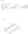
- FIG. 1 is a sectional view illustrating a backlight unit according to one example not forming part of the invention .
- the backlight unit includes a bottom chassis 110, a reflective sheet 120, a light guide plate 130, an optical sheet 140, a printed circuit board 150, Light Emitting Diode packages 160 and a shock-absorbing member 180.
- the light guide plate 130 and the optical sheet 140 may be referred to optical members.
- the bottom chassis 110 is configured to receive the reflective sheet 120, the light guide plate 130, the optical sheet 140, the printed circuit board 150 and the LED packages 160.
- the bottom chassis 110 is made of a metal, such as aluminum, zinc, copper, iron, stainless steel and alloys thereof.
- the LED packages 160 are mounted on one surface of the printed circuit board 150 and serve to emit light.
- the LED packages 160 mounted on the printed circuit board 150 are referred to an LED package module.
- the other surface of the printed circuit board 150 is fixed to a guide panel 114 defining a sidewall of the bottom chassis 110.
- the light guide plate 130 is disposed within the bottom chassis 110 such that a light incident surface of the light guide plate 130 faces the LED packages 160, thereby serving to receive the light emitted from the LED packages 160 and guide the light in a given direction.
- the reflective sheet 120 is disposed between the bottom chassis 110 and the light guide plate 130 and functions to reflect the light exiting a rear surface of the light guide plate 130 so as to reintroduce the light into the light guide plate 130.
- the optical sheet 140 is disposed above the light guide plate 130 and serves to improve properties of the light having passed therethrough.
- the bottom chassis 110 is provided with at least one first protrusion 112 to support the reflective sheet 120 and the light guide plate 130.
- the at least one first protrusion 112 serves to position the light guide plate 130 such that the light incident surface of the light guide plate 130 faces the LED packages 160.
- the first protrusion 112 may take the form of a line extending in a direction perpendicular to the light incident surface of the light guide plate 130 and may include two or more first protrusions spaced apart from each other.
- the shock-absorbing member 180 contacts with a surface of the first protrusion 112 and the other surface of the shock-absorbing member 180 contacts with the reflective sheet 120.
- the shock-absorbing member 180 is disposed in a region of the optical member. Specifically, the shock-absorbing member 180 may come into direct contact with the optical member, or may spatially correspond to the optical member.
- the shock-absorbing member 180 may be made of various materials.
- the shock-absorbing member 180 may take the form of an insulating tape and may be made of rubber, silicone or the like.
- the shock-absorbing member 180 may prevent damage to the reflective sheet 120 in contact therewith and the light guide plate 130 disposed on the reflective sheet 120 due to shock or heat transferred from the bottom chassis 110.
- shock-absorbing member 180 may exhibit frictional force to prevent unwanted movement of the reflective sheet 120 in contact therewith and/or the light guide plate 130 disposed on the reflective sheet 120.
- the light guide plate 130 is disposed such that the light incident surface thereof is close to the LED packages 160. If the light guide plate 130 is moved, the light incident surface of the light guide plate 130 may be damaged due to collision with the LED packages 160 and color uniformity of the backlight unit may be deteriorated.
- FIG. 2 is a view illustrating the shock-absorbing member 180 in contact with the bottom chassis 110 illustrated in FIG. 1 .
- the shock-absorbing member 180 is formed at a surface of the line-shaped first protrusion 112 and thus, may have a line form.
- the first protrusion 112 formed at the bottom chassis 110 may take the form of a line having a predetermined length L and width W, which extends in a direction parallel to the light incident surface of the light guide plate 130, and the shock-absorbing member 180 contacts with an upper surface of the first protrusion 112.
- FIG. 2 illustrates the first protrusion 112 and the shock-absorbing member 180 formed on the bottom chassis 110 as respectively taking the form of two lines, the number and shape thereof are not limited thereto.
- FIG. 3 is a sectional view of a backlight unit according to another example not forming part of the invention .
- the backlight unit includes a bottom chassis 310, the reflective sheet 120, the light guide plate 130, the optical sheet 140, the printed circuit board 150, the LED packages 160 and a shock-absorbing member 380.
- the bottom chassis 310 illustrated in FIG. 3 has a flat inner surface without the first protrusion.
- One surface of the shock-absorbing member 380 contacts with the flat surface of the bottom chassis 310 and the other surface of the shock-absorbing member 380 contacts with the reflective sheet 120.
- the reflective sheet 120, the light guide plate 130, the optical sheet 140, the printed circuit board 150 and the LED packages 160 are identical to those as described in relation to FIG. 1 and thus, a description thereof will be omitted to avoid repetition.
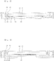
- FIG. 4 is a sectional view of a backlight unit according to an embodiment.
- the backlight unit includes a bottom chassis 410, a bracket 420, a printed circuit board 430, LED packages 435, a shock-absorbing member 440 (hereinafter, referred to a first shock-absorbing member that is distinguished from a second shock-absorbing member), a reflective sheet 445, a light guide plate 450, an optical sheet 460 and a second shock-absorbing member 490.
- the bottom chassis 410 is configured to receive constituent elements of the backlight unit.
- the reflective sheet 445, the light guide plate 450 and the optical sheet 460 are sequentially received within the bottom chassis 410.
- the bottom chassis 410 serves to support the reflective sheet 445 and the light guide plate 450.
- the bottom chassis 410 includes an outer portion surrounding the bracket 420 and a rear surface portion having a first protrusion protruding toward the reflective sheet 445 and the light guide plate 450.
- the first protrusion serves to support the reflective sheet 445.
- the first shock-absorbing member 440 contacts with a surface of the first protrusion of the bottom chassis 410. Specifically, the first shock-absorbing member 440 is disposed between the first protrusion of the bottom chassis 410 and the reflective sheet 445 and the reflective sheet 445 comes into close contact with the first shock-absorbing member 440.
- the first shock-absorbing member 440 may come into contact with a front surface or a partial region of the protrusion of the bottom chassis 410. Also, the first shock-absorbing member 440 may include a single line-shaped shock-absorbing member, or a plurality of line-shaped shock-absorbing members spaced apart from one another so as to come into contact with the surface of the first protrusion.
- the LED packages 435 are mounted on one surface of the printed circuit board 430 and emit light to a light incident surface of the light guide plate 450.
- the other surface of the printed circuit board 430 is fixed to the corresponding bracket 420.
- the light guide plate 450 is disposed within the bottom chassis 410 and serves to receive the light emitted from the LED packages 160 and guide the light in a given direction. Specifically, the light guide plate 450 converts linear light emitted from the LED packages 435 to planar light so as to transmit uniform light to a screen display region (for example, a liquid crystal panel).
- the light guide plate 450 is typically made of transparent acryl and has a thickness of about several millimeters.
- a lower surface of the light guide plate 450 may be provided with a plurality of dots or V-shaped holes (not shown) for uniform light reflection.
- the reflective sheet 445 is disposed between the bottom chassis 410 and the light guide plate 450 and reflects the light exiting a rear surface of the light guide plate 450 so as to reintroduce the light into the light guide plate 450.
- the bracket 420 to which the printed circuit board 430 provided with the LED packages 435 is fixed, is disposed adjacent to one side surface (i.e. the light incident surface) of the light guide plate 450 and functions to dissipate heat from the LED packages 435 and the printed circuit board 430.
- both the bracket 420 and the guide panel 114 of the above described embodiment can function to support the LED package module including light emitting devices while coming into contact with the bottom chassis 410 and thus, may be referred to supporting members.
- the bracket 420 includes a vertical portion and a horizontal portion connected thereto.
- the vertical portion has at least one bent portion.
- the printed circuit board 430 is fixed to the vertical portion of the bracket 420 and the horizontal portion of the bracket 420 is disposed between edge regions of the reflective sheet 445 and the bottom chassis 410.
- the edge regions mean regions adjacent to an edge region of the light guide plate 450.
- the bracket 420 may have various shapes.
- the bracket 420 may have an "L"-shaped form.
- the vertical portion of the bracket 420 may have an inverted "U"-shaped form.
- the bracket 420 is provided at a surface of the horizontal portion thereof with a second protrusion 480 that serves to support the reflective sheet 445 and the light guide plate 450 disposed on the reflective sheet 445.
- FIG. 4 illustrates only one second protrusion 480, the embodiment is not limited thereto.
- the second protrusion 480 may take the form of a line having a predetermined length and width, which extends in a direction parallel to the light incident surface of the light guide plate 130.
- the second shock-absorbing member 490 contacts with an upper surface of the second protrusion 480. Specifically, the second shock-absorbing member 490 is disposed between the second protrusion 480 and the reflective sheet 445 and the reflective sheet 445 comes into close contact with the second shock-absorbing member 490.
- FIG. 4 illustrates the backlight unit including both the first shock-absorbing member 440 and the second shock-absorbing member 490
- the embodiment is not limited thereto, and any one of the first shock-absorbing member 440 and the second shock-absorbing member 490 may be omitted.
- the first shock-absorbing member 440 and the second shock-absorbing member 490 may be made of rubber, silicone or the like.
- the first shock-absorbing member 440 and the second shock-absorbing member 490 may take the form of a double-sided adhesive tape.
- the first shock-absorbing member 440 and the second shock-absorbing member 490 may serve to control thicknesses of the reflective sheet 445 and the light guide plate 450, thereby positioning the light guide plate 450 such that the light incident surface of the light guide plate 450 is parallel to the LED packages 435.
- the first shock-absorbing member 440 and the second shock-absorbing member 490 may prevent the reflective sheet 445 and the light guide plate 450 from being damaged by shock or heat transferred from the bottom chassis 410.
- the first shock-absorbing member 440 and the second shock-absorbing member 490 may also prevent unwanted movement of the reflective sheet 445 in contact therewith and the light guide plate 450 disposed on the reflective sheet 445.
- the optical sheet 460 is disposed on the light guide plate 450.
- the optical sheet 460 may include a diffusion sheet to diffuse light directed from the light guide plate 450 and a prismatic sheet to vertically emit light directed from the diffusion sheet. Two or three diffusion and prismatic sheets may be appropriately combined with one another.
- the optical sheet 460 may further include a protective sheet disposed on the diffusion sheet or the prismatic sheet.
- the protective sheet serves to protect the diffusion sheet and the prismatic sheet that are sensitive to dust or scratches and to prevent movement of the diffusion sheet and the prismatic sheet during transportation of the backlight unit.
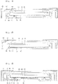
- FIG. 5 is a sectional view of a backlight unit according to another example not forming part of the invention .
- the backlight unit includes a bottom chassis 510, a bracket 520, the printed circuit board 430, the LED packages 435, the reflective sheet 445, the light guide plate 450, the optical sheet 460 and shock-absorbing member 540.
- the bracket 520 illustrated in FIG. 5 has no second protrusion at a surface of a horizontal portion thereof, the bottom chassis 510 is provided with at least one first protrusion 530.
- the first protrusion 530 is formed at an edge region thereof adjacent to the edge region of the light guide plate 450, rather than being provided at the center of the bottom chassis 510.
- the shock-absorbing member 540 is formed at a surface of the first protrusion.
- FIG. 6 is a sectional view of a backlight unit according to another example not forming part of the invention .
- a bottom chassis 610 is provided with a first protrusion protruding toward the reflective sheet 445 and the light guide plate 450 and differently from FIG. 5 , the first protrusion is formed at the center of a rear surface portion of the bottom chassis 610 rather than being formed at an edge region of the rear surface portion.
- a shock-absorbing member 620 is formed at a surface of the first protrusion.
- FIGs. 7 to 8 and 10 to 11 are sectional views illustrating display devices according to other examples not forming part of the invention and FIG. 9 is a sectional view illustrating a display device according to another embodiment .
- FIG. 7 illustrates a display device including the backlight unit illustrated in FIG. 1
- FIG. 8 illustrates a display device including the backlight unit illustrated in FIG. 3
- FIG. 9 illustrates a display device including the backlight unit illustrated in FIG. 4
- FIG. 10 illustrates a display device including the backlight unit illustrated in FIG. 5
- FIG. 11 illustrates a display device including the backlight unit illustrated in FIG. 6 .
- the display device includes the backlight unit, a mold frame 465, a liquid crystal panel 470 and a top chassis 485.
- the backlight unit is any one of those illustrated in FIGs. 1 , 3 , and 4 to 6 .
- the mold frame 465 is disposed to surround a sidewall of the bottom chassis 410 and an edge region of the optical sheet 460.
- the liquid crystal panel 470 is seated on an upper end of the mold frame 465 so as to be disposed on an upper surface (or a front surface) of the optical sheet 460.
- the liquid crystal panel 470 is configured such that liquid crystals are filled between glass substrates and polarizing plates are disposed respectively on both the glass substrates to polarize light.
- the liquid crystals are regularly arranged organic molecules having properties between solid and liquid and thus, having fluidity.
- the molecular arrangement of liquid crystals is changed by an exterior electric field, enabling display of an image.
- a color filter (not shown) may be provided on a front surface of the liquid crystal panel 470.
- the top chassis 485 is disposed to surround the mold frame 465 and an edge region of the liquid crystal panel 470.
- the mold frame 465 and the top chassis 485 respectively have central openings to expose a display region of the liquid crystal panel 470.
- any reference in this specification to "one embodiment,” “an embodiment,” “example embodiment,” etc. means that a particular feature, structure, or characteristic described in connection with the embodiment is included in at least one embodiment.
- the appearances of such phrases in various places in the specification are not necessarily all referring to the same embodiment.
Landscapes
- Physics & Mathematics (AREA)
- General Physics & Mathematics (AREA)
- Optics & Photonics (AREA)
- Planar Illumination Modules (AREA)
- Liquid Crystal (AREA)
Description
- The invention relates to a backlight unit and a display device.
- Generally, Liquid Crystal Displays (LCDs) have higher visibility than Cathode Ray Tubes (CRTs) and less average power consumption and heat emission than the same screen size of CRTs. For this reason, LCDs have been widely used in mobile phones, computer monitors and televisions, along with plasma display devices or field emission display devices.
- The driving principle of LCDs is based on optical isotropy and polarization of liquid crystals. Elongated liquid crystals exhibit directivity in molecular arrangement. Here, the molecular arrangement direction of liquid crystals may be controlled by applying an electric field to liquid crystals.
- Accordingly, controlling the molecular arrangement direction of liquid crystals may change molecular arrangement of liquid crystals, whereby image information can be displayed as light is refracted in the molecular arrangement direction of liquid crystals by optical isotropy.
- However, LCDs are non-self emissive devices and require a separate light source. One example of the light source is a backlight unit. Specifically, light emitted from a backlight unit disposed behind a liquid crystal panel is introduced into the liquid crystal panel, such that transmittance of light is controlled based on the arrangement of liquid crystals, enabling display of an image.
-
US2006023139 A1 relates to a liquid crystal display panel comprising a light emitting device, a light guide plate to guide light emitted from the light emitting device, a bottom chassis disposed on a rear surface of the light guide plate, a reflective sheet disposed below the light guide plate and a first shock-absorbing member disposed between the rear surface of the reflective sheet and the bottom chassis, wherein the first shock-absorbing member directly contacts with the reflective sheet. -
WO2009008617 A2 relates to a display device comprising a light emitting device, a light guide plate to guide the light emitted from the light emitting device, a bottom chassis disposed on a rear surface of the light guide plate, a reflective sheet disposed below the light guide plate, wherein the bottom chassis has a first protrusion protruding toward the reflective sheet and a bracket contacting with the bottom chassis, the bracket including a horizontal portion and a module including the light emitting device. -
US2009231513 (A1 ) relates to a backlight unit comprising a light emitting device, a light guide plate to guide the light emitted from the light emitting device, a bottom chassis disposed on a rear surface of the light guide plate, a reflective sheet disposed below the light guide plate and a bracket contacting with the bottom chassis, the bracket including a vertical portion perpendicular to the bottom chassis and a module including the light emitting device. -
US2006033412 (A1 ) relates to a backlight assembly and liquid crystal display apparatus comprising a light emitting device, a light guide plate to guide the light emitted from the light emitting device, a bottom chassis disposed on a rear surface of the light guide plate, a bracket contacting with the bottom chassis, the bracket including a vertical portion perpendicular to the bottom chassis and a horizontal portion connected to the vertical portion, wherein the bracket has two second protrusions protruding toward the reflective sheet, and two second shock-absorbing members each disposed between the rear surface of the reflective sheet and a corresponding one of the two second protrusions. - Accordingly, the invention is directed to a backlight unit and a display device that substantially obviate one or more problems due to limitations and disadvantages of the related art.
- An object of the invention is to provide a backlight unit and a display device capable of preventing damage due to movement of a light guide plate.
- Additional advantages, objects, and features of the invention will be set forth in part in the description which follows and in part will become apparent to those having ordinary skill in the art upon examination of the following or may be learned from practice of the invention . The objectives and other advantages of the invention may be realized and attained by the structure particularly pointed out in the written description and claims hereof as well as the appended drawings.
- To achieve these objects and other advantages and in accordance with the purpose of the invention, as embodied and broadly described herein, a backlight unit is provided according to claim 1.
- Further embodiments are presented in the dependent claims.
- It is to be understood that both the foregoing general description and the following detailed description of the embodiment are exemplary and explanatory and are intended to provide further explanation of the embodiment as claimed.
- The accompanying drawings, which are included to provide a further understanding of the embodiment and are incorporated in and constitute a part of this application, illustrate embodiment(s) and together with the description serve to explain the principle of the embodiment. In the drawings:
-
FIG. 1 is a sectional view illustrating a backlight unit according to one example not forming part of the invention ; -
FIG. 2 is a perspective view illustrating a shock-absorbing member in contact with a bottom chassis illustrated inFIG. 1 ; -
FIG. 3 is a sectional view of a backlight unit according to another example not forming part of the invention ; -
FIG. 4 is a sectional view of a backlight unit according to an embodiment; -
FIG. 5 is a sectional view of a backlight unit accrding to another example not forming part of the invention ; -
FIG. 6 is a sectional view of a backlight unit according to another example not forming part of the invention ; and -
FIGs. 7 to 8 and10 to 11 are sectional views illustrating display devices according to other examples not forming part of the invention andFIG. 9 is a sectional view illustrating a display device according to another embodiment. - In the description of the embodiments, it will be understood that, when a layer (or film), a region, a pattern, or a structure is referred to as being "on" or "under" another substrate, another layer (or film), another region, another pad, or another pattern, it can be "directly" or "indirectly" over the other substrate, layer (or film), region, pad, or pattern, or one or more intervening layers may also be present. Such a position of the layer has been described with reference to the drawings.
- The thickness and size of each layer shown in the drawings may be exaggerated, omitted or schematically drawn for the purpose of convenience or clarity. In addition, the size of elements does not utterly reflect an actual size.
- Hereinafter, a light emitting device and a method of manufacturing the same according to the embodiment will be described with reference to accompanying drawings.
-
FIG. 1 is a sectional view illustrating a backlight unit according to one example not forming part of the invention . The backlight unit includes abottom chassis 110, areflective sheet 120, alight guide plate 130, anoptical sheet 140, a printedcircuit board 150, LightEmitting Diode packages 160 and a shock-absorbingmember 180. Here, thelight guide plate 130 and theoptical sheet 140 may be referred to optical members. - The
bottom chassis 110 is configured to receive thereflective sheet 120, thelight guide plate 130, theoptical sheet 140, the printedcircuit board 150 and theLED packages 160. Thebottom chassis 110 is made of a metal, such as aluminum, zinc, copper, iron, stainless steel and alloys thereof. - The
LED packages 160 are mounted on one surface of the printedcircuit board 150 and serve to emit light. In this case, theLED packages 160 mounted on the printedcircuit board 150 are referred to an LED package module. - The other surface of the printed
circuit board 150 is fixed to aguide panel 114 defining a sidewall of thebottom chassis 110. Thelight guide plate 130 is disposed within thebottom chassis 110 such that a light incident surface of thelight guide plate 130 faces theLED packages 160, thereby serving to receive the light emitted from theLED packages 160 and guide the light in a given direction. - The
reflective sheet 120 is disposed between thebottom chassis 110 and thelight guide plate 130 and functions to reflect the light exiting a rear surface of thelight guide plate 130 so as to reintroduce the light into thelight guide plate 130. Theoptical sheet 140 is disposed above thelight guide plate 130 and serves to improve properties of the light having passed therethrough. - The
bottom chassis 110 is provided with at least onefirst protrusion 112 to support thereflective sheet 120 and thelight guide plate 130. In addition, the at least onefirst protrusion 112 serves to position thelight guide plate 130 such that the light incident surface of thelight guide plate 130 faces theLED packages 160. For example, thefirst protrusion 112 may take the form of a line extending in a direction perpendicular to the light incident surface of thelight guide plate 130 and may include two or more first protrusions spaced apart from each other. - One surface of the shock-absorbing
member 180 contacts with a surface of thefirst protrusion 112 and the other surface of the shock-absorbingmember 180 contacts with thereflective sheet 120. The shock-absorbingmember 180 is disposed in a region of the optical member. Specifically, the shock-absorbingmember 180 may come into direct contact with the optical member, or may spatially correspond to the optical member. - The shock-absorbing
member 180 may be made of various materials. For example, the shock-absorbingmember 180 may take the form of an insulating tape and may be made of rubber, silicone or the like. - The shock-absorbing
member 180 may prevent damage to thereflective sheet 120 in contact therewith and thelight guide plate 130 disposed on thereflective sheet 120 due to shock or heat transferred from thebottom chassis 110. - In addition, the shock-absorbing
member 180 may exhibit frictional force to prevent unwanted movement of thereflective sheet 120 in contact therewith and/or thelight guide plate 130 disposed on thereflective sheet 120. - The
light guide plate 130 is disposed such that the light incident surface thereof is close to theLED packages 160. If thelight guide plate 130 is moved, the light incident surface of thelight guide plate 130 may be damaged due to collision with theLED packages 160 and color uniformity of the backlight unit may be deteriorated. -
FIG. 2 is a view illustrating the shock-absorbingmember 180 in contact with thebottom chassis 110 illustrated inFIG. 1 . Referring toFIG. 2 , the shock-absorbingmember 180 is formed at a surface of the line-shapedfirst protrusion 112 and thus, may have a line form. In this case, thefirst protrusion 112 formed at thebottom chassis 110 may take the form of a line having a predetermined length L and width W, which extends in a direction parallel to the light incident surface of thelight guide plate 130, and the shock-absorbingmember 180 contacts with an upper surface of thefirst protrusion 112. AlthoughFIG. 2 illustrates thefirst protrusion 112 and the shock-absorbingmember 180 formed on thebottom chassis 110 as respectively taking the form of two lines, the number and shape thereof are not limited thereto. -
FIG. 3 is a sectional view of a backlight unit according to another example not forming part of the invention . Referring toFIG. 3 , the backlight unit includes abottom chassis 310, thereflective sheet 120, thelight guide plate 130, theoptical sheet 140, the printedcircuit board 150, the LED packages 160 and a shock-absorbingmember 380. - Differently from
FIG. 1 , thebottom chassis 310 illustrated inFIG. 3 has a flat inner surface without the first protrusion. One surface of the shock-absorbingmember 380 contacts with the flat surface of thebottom chassis 310 and the other surface of the shock-absorbingmember 380 contacts with thereflective sheet 120. Thereflective sheet 120, thelight guide plate 130, theoptical sheet 140, the printedcircuit board 150 and the LED packages 160 are identical to those as described in relation toFIG. 1 and thus, a description thereof will be omitted to avoid repetition. -
FIG. 4 is a sectional view of a backlight unit according to an embodiment. Referring toFIG. 4 , the backlight unit includes abottom chassis 410, abracket 420, a printedcircuit board 430, LED packages 435, a shock-absorbing member 440 (hereinafter, referred to a first shock-absorbing member that is distinguished from a second shock-absorbing member), areflective sheet 445, alight guide plate 450, anoptical sheet 460 and a second shock-absorbingmember 490. - The
bottom chassis 410 is configured to receive constituent elements of the backlight unit. Thereflective sheet 445, thelight guide plate 450 and theoptical sheet 460 are sequentially received within thebottom chassis 410. Thebottom chassis 410 serves to support thereflective sheet 445 and thelight guide plate 450. - The
bottom chassis 410 includes an outer portion surrounding thebracket 420 and a rear surface portion having a first protrusion protruding toward thereflective sheet 445 and thelight guide plate 450. The first protrusion serves to support thereflective sheet 445. - The first shock-absorbing
member 440 contacts with a surface of the first protrusion of thebottom chassis 410. Specifically, the first shock-absorbingmember 440 is disposed between the first protrusion of thebottom chassis 410 and thereflective sheet 445 and thereflective sheet 445 comes into close contact with the first shock-absorbingmember 440. - The first shock-absorbing
member 440 may come into contact with a front surface or a partial region of the protrusion of thebottom chassis 410. Also, the first shock-absorbingmember 440 may include a single line-shaped shock-absorbing member, or a plurality of line-shaped shock-absorbing members spaced apart from one another so as to come into contact with the surface of the first protrusion. - The LED packages 435 are mounted on one surface of the printed
circuit board 430 and emit light to a light incident surface of thelight guide plate 450. The other surface of the printedcircuit board 430 is fixed to thecorresponding bracket 420. - The
light guide plate 450 is disposed within thebottom chassis 410 and serves to receive the light emitted from the LED packages 160 and guide the light in a given direction. Specifically, thelight guide plate 450 converts linear light emitted from the LED packages 435 to planar light so as to transmit uniform light to a screen display region (for example, a liquid crystal panel). Thelight guide plate 450 is typically made of transparent acryl and has a thickness of about several millimeters. A lower surface of thelight guide plate 450 may be provided with a plurality of dots or V-shaped holes (not shown) for uniform light reflection. - The
reflective sheet 445 is disposed between thebottom chassis 410 and thelight guide plate 450 and reflects the light exiting a rear surface of thelight guide plate 450 so as to reintroduce the light into thelight guide plate 450. - The
bracket 420, to which the printedcircuit board 430 provided with the LED packages 435 is fixed, is disposed adjacent to one side surface (i.e. the light incident surface) of thelight guide plate 450 and functions to dissipate heat from the LED packages 435 and the printedcircuit board 430. - Here, both the
bracket 420 and theguide panel 114 of the above described embodiment can function to support the LED package module including light emitting devices while coming into contact with thebottom chassis 410 and thus, may be referred to supporting members. - The
bracket 420 includes a vertical portion and a horizontal portion connected thereto. The vertical portion has at least one bent portion. - The printed
circuit board 430 is fixed to the vertical portion of thebracket 420 and the horizontal portion of thebracket 420 is disposed between edge regions of thereflective sheet 445 and thebottom chassis 410. In this case, the edge regions mean regions adjacent to an edge region of thelight guide plate 450. - The
bracket 420 may have various shapes. For example, thebracket 420 may have an "L"-shaped form. Alternatively, as illustrated inFIG. 4 , the vertical portion of thebracket 420 may have an inverted "U"-shaped form. - The
bracket 420 is provided at a surface of the horizontal portion thereof with asecond protrusion 480 that serves to support thereflective sheet 445 and thelight guide plate 450 disposed on thereflective sheet 445. AlthoughFIG. 4 illustrates only onesecond protrusion 480, the embodiment is not limited thereto. - The
second protrusion 480 may take the form of a line having a predetermined length and width, which extends in a direction parallel to the light incident surface of thelight guide plate 130. The second shock-absorbingmember 490 contacts with an upper surface of thesecond protrusion 480. Specifically, the second shock-absorbingmember 490 is disposed between thesecond protrusion 480 and thereflective sheet 445 and thereflective sheet 445 comes into close contact with the second shock-absorbingmember 490. - Although
FIG. 4 illustrates the backlight unit including both the first shock-absorbingmember 440 and the second shock-absorbingmember 490, the embodiment is not limited thereto, and any one of the first shock-absorbingmember 440 and the second shock-absorbingmember 490 may be omitted. - The first shock-absorbing
member 440 and the second shock-absorbingmember 490 may be made of rubber, silicone or the like. The first shock-absorbingmember 440 and the second shock-absorbingmember 490 may take the form of a double-sided adhesive tape. - In addition to supporting the
reflective sheet 445 and thelight guide plate 450, the first shock-absorbingmember 440 and the second shock-absorbingmember 490 may serve to control thicknesses of thereflective sheet 445 and thelight guide plate 450, thereby positioning thelight guide plate 450 such that the light incident surface of thelight guide plate 450 is parallel to the LED packages 435. - The first shock-absorbing
member 440 and the second shock-absorbingmember 490 may prevent thereflective sheet 445 and thelight guide plate 450 from being damaged by shock or heat transferred from thebottom chassis 410. The first shock-absorbingmember 440 and the second shock-absorbingmember 490 may also prevent unwanted movement of thereflective sheet 445 in contact therewith and thelight guide plate 450 disposed on thereflective sheet 445. - The
optical sheet 460 is disposed on thelight guide plate 450. Theoptical sheet 460 may include a diffusion sheet to diffuse light directed from thelight guide plate 450 and a prismatic sheet to vertically emit light directed from the diffusion sheet. Two or three diffusion and prismatic sheets may be appropriately combined with one another. - The
optical sheet 460 may further include a protective sheet disposed on the diffusion sheet or the prismatic sheet. The protective sheet serves to protect the diffusion sheet and the prismatic sheet that are sensitive to dust or scratches and to prevent movement of the diffusion sheet and the prismatic sheet during transportation of the backlight unit. -
FIG. 5 is a sectional view of a backlight unit according to another example not forming part of the invention . Referring toFIG. 5 , the backlight unit includes abottom chassis 510, abracket 520, the printedcircuit board 430, the LED packages 435, thereflective sheet 445, thelight guide plate 450, theoptical sheet 460 and shock-absorbingmember 540. - Differently from
FIG. 4 , thebracket 520 illustrated inFIG. 5 has no second protrusion at a surface of a horizontal portion thereof, thebottom chassis 510 is provided with at least onefirst protrusion 530. In the present example not forming part of the invention , thefirst protrusion 530 is formed at an edge region thereof adjacent to the edge region of thelight guide plate 450, rather than being provided at the center of thebottom chassis 510. The shock-absorbingmember 540 is formed at a surface of the first protrusion. -
FIG. 6 is a sectional view of a backlight unit according to another example not forming part of the invention . Referring toFIG. 6 , abottom chassis 610 is provided with a first protrusion protruding toward thereflective sheet 445 and thelight guide plate 450 and differently fromFIG. 5 , the first protrusion is formed at the center of a rear surface portion of thebottom chassis 610 rather than being formed at an edge region of the rear surface portion. A shock-absorbingmember 620 is formed at a surface of the first protrusion. -
FIGs. 7 to 8 and10 to 11 are sectional views illustrating display devices according to other examples not forming part of the invention andFIG. 9 is a sectional view illustrating a display device according to another embodiment .FIG. 7 illustrates a display device including the backlight unit illustrated inFIG. 1 ,FIG. 8 illustrates a display device including the backlight unit illustrated inFIG. 3 ,FIG. 9 illustrates a display device including the backlight unit illustrated inFIG. 4 ,FIG. 10 illustrates a display device including the backlight unit illustrated inFIG. 5 , andFIG. 11 illustrates a display device including the backlight unit illustrated inFIG. 6 . - Referring to
FIGs. 7 to 11 , the display device includes the backlight unit, amold frame 465, aliquid crystal panel 470 and atop chassis 485. In this case, the backlight unit is any one of those illustrated inFIGs. 1 ,3 , and4 to 6 . - The
mold frame 465 is disposed to surround a sidewall of thebottom chassis 410 and an edge region of theoptical sheet 460. Theliquid crystal panel 470 is seated on an upper end of themold frame 465 so as to be disposed on an upper surface (or a front surface) of theoptical sheet 460. Theliquid crystal panel 470 is configured such that liquid crystals are filled between glass substrates and polarizing plates are disposed respectively on both the glass substrates to polarize light. Here, the liquid crystals are regularly arranged organic molecules having properties between solid and liquid and thus, having fluidity. The molecular arrangement of liquid crystals is changed by an exterior electric field, enabling display of an image. A color filter (not shown) may be provided on a front surface of theliquid crystal panel 470. - The
top chassis 485 is disposed to surround themold frame 465 and an edge region of theliquid crystal panel 470. Themold frame 465 and thetop chassis 485 respectively have central openings to expose a display region of theliquid crystal panel 470. - Any reference in this specification to "one embodiment," "an embodiment," "example embodiment," etc., means that a particular feature, structure, or characteristic described in connection with the embodiment is included in at least one embodiment. The appearances of such phrases in various places in the specification are not necessarily all referring to the same embodiment. Further, when a particular feature, structure, or characteristic is described in connection with any embodiment, it is submitted that it is within the purview of one skilled in the art to effect such feature, structure, or characteristic in connection with other ones of the embodiments.
- Although embodiments have been described with reference to a number of illustrative embodiments thereof, it should be understood that numerous other modifications and embodiments can be devised by those skilled in the art that will fall within the scope of the principles of this disclosure. More particularly, various variations and modifications are possible in the component parts and/or arrangements of the subject combination arrangement within the scope of the disclosure, the drawings and the appended claims. In addition to variations and modifications in the component parts and/or arrangements, alternative uses will also be apparent to those skilled in the art.
Claims (6)
- A backlight unit comprising:a light emitting device;a light guide plate (450) to guide the light emitted from the light emitting device;a bottom chassis (410) disposed on a rear surface of the light guide plate (450);a bracket (420) contacting with the bottom chassis (410), the bracket (420) including a vertical portion perpendicular to the bottom chassis (410), a horizontal portion connected to the vertical portion, and a module including the light emitting device disposed on the bracket (420);a reflective sheet (445) disposed below the light guide plate (450), wherein the bottom chassis (410) has a first protrusion protruding toward the reflective sheet (445), and the bracket (420) has two second protrusions (480) protruding toward the reflective sheet (445);a first shock-absorbing member (440) disposed between the rear surface of the reflective sheet (445) and the first protrusion, the first shock-absorbing member (440) directly contacts with the reflective sheet (445) and the first protrusion; andtwo second shock-absorbing members (490) each being disposed between the rear surface of the reflective sheet (445) and a corresponding one of the two second protrusions (480), wherein each second shock-absorbing member (490) directly contacts with the reflective sheet (445) and the corresponding one of the two second protrusions (480), andwherein a width of the first shock-absorbing member (440) is greater than a width of each of the two second shock-absorbing members (490).
- The backlight unit according to claim 1, wherein the first shock-absorbing member (440) and each of the two second shock-absorbing members (490) are disposed in a region of the light guide plate.
- The backlight unit according to claim 1, wherein each of the first shock-absorbing member (440) and each of the two second shock-absorbing members (490) have the form of a line.
- The backlight unit according to claim 1, wherein the first shock-absorbing member (440) and each of the two second shock-absorbing members (490) have the form of lines facing each other.
- The backlight unit according to claim 1, wherein the first shock-absorbing member (440) and each of the two second shock-absorbing members (490) are an insulating tape.
- A display device comprising:a backlight unit according to any one of claims 1 to 5; anda liquid crystal panel (470) disposed on the backlight unit.
Applications Claiming Priority (1)
| Application Number | Priority Date | Filing Date | Title |
|---|---|---|---|
| KR1020100048498 | 2010-05-25 |
Publications (2)
| Publication Number | Publication Date |
|---|---|
| EP2390693A1 EP2390693A1 (en) | 2011-11-30 |
| EP2390693B1 true EP2390693B1 (en) | 2022-11-23 |
Family
ID=44117876
Family Applications (1)
| Application Number | Title | Priority Date | Filing Date |
|---|---|---|---|
| EP11167045.1A Active EP2390693B1 (en) | 2010-05-25 | 2011-05-23 | Backlight unit and display device |
Country Status (4)
| Country | Link |
|---|---|
| US (2) | US20110292317A1 (en) |
| EP (1) | EP2390693B1 (en) |
| JP (1) | JP5864132B2 (en) |
| CN (1) | CN102297361B (en) |
Families Citing this family (31)
| Publication number | Priority date | Publication date | Assignee | Title |
|---|---|---|---|---|
| JP5636878B2 (en) * | 2010-10-29 | 2014-12-10 | ソニー株式会社 | Display device, lighting device and casing |
| US9322980B2 (en) * | 2011-10-06 | 2016-04-26 | Sharp Kabushiki Kaisha | Illumination device, display device, and television receiving device |
| US9621838B2 (en) | 2011-10-25 | 2017-04-11 | Funai Electric Co., Ltd. | Display device and television apparatus |
| CN102537882B (en) * | 2011-12-13 | 2014-11-05 | 深圳市华星光电技术有限公司 | Back plate and corresponding backlight module |
| US8801263B2 (en) | 2011-12-13 | 2014-08-12 | Shenzhen China Star Optoelectronics Technology Co., Ltd. | Backplate and backlight module comprising the same |
| US8905618B2 (en) * | 2012-03-13 | 2014-12-09 | Shenzhen China Star Optoelectronics Technology Co., Ltd. | Combined backplane and backlight module using same |
| JP2013238639A (en) * | 2012-05-11 | 2013-11-28 | Sharp Corp | Display device and television receiver |
| US8982298B2 (en) * | 2012-07-02 | 2015-03-17 | Shenzhen China Star Optoelectronics Technology Co., Ltd. | Liquid crystal display comprising springs that horizontally expand and contract a third backplane unit relative to a first and second backplane |
| US8834006B2 (en) * | 2012-07-24 | 2014-09-16 | Shenzhen China Star Optoelectronics Technology Co., Ltd | Backlight module and liquid crystal display device |
| KR101911902B1 (en) * | 2012-07-25 | 2018-10-26 | 삼성디스플레이 주식회사 | Shock absorbing member and display device comprising the same |
| CN102788297B (en) * | 2012-07-31 | 2014-08-06 | 深圳市华星光电技术有限公司 | Backlight module, as well as assembly method and assembly jig for same |
| US9110198B2 (en) * | 2012-09-26 | 2015-08-18 | Shenzhen China Star Optoelectronics Technology Co., Ltd. | Backlight module |
| TWI495933B (en) * | 2012-10-17 | 2015-08-11 | Au Optronics Corp | Display apparatus |
| KR102049854B1 (en) * | 2013-01-23 | 2019-11-28 | 엘지전자 주식회사 | Apparatus for planar lighting |
| JP2014170079A (en) * | 2013-03-01 | 2014-09-18 | Funai Electric Co Ltd | Display device |
| JP6167629B2 (en) * | 2013-04-12 | 2017-07-26 | 船井電機株式会社 | Display device |
| US9632237B2 (en) | 2013-06-07 | 2017-04-25 | Sharp Kabushiki Kaisha | Illumination device, display device, and TV receiver |
| JP6366931B2 (en) * | 2013-12-06 | 2018-08-01 | シャープ株式会社 | Liquid crystal display |
| WO2015114769A1 (en) * | 2014-01-30 | 2015-08-06 | 堺ディスプレイプロダクト株式会社 | Light source apparatus and display apparatus |
| TWI544173B (en) * | 2014-06-17 | 2016-08-01 | 緯創資通股份有限公司 | Black light module with mount and displaying apparatus therewith |
| KR102304267B1 (en) | 2014-11-19 | 2021-09-23 | 쑤저우 레킨 세미컨덕터 컴퍼니 리미티드 | Light emitting device package and backlight unit including the package |
| KR20170068695A (en) * | 2015-12-09 | 2017-06-20 | 삼성디스플레이 주식회사 | Display device |
| US20170212381A1 (en) * | 2016-01-27 | 2017-07-27 | Motorola Mobility Llc | Liquid Crystal Display Without Bezel |
| KR102552047B1 (en) | 2016-11-24 | 2023-07-07 | 엘지디스플레이 주식회사 | Display device |
| CN109611716A (en) * | 2017-10-04 | 2019-04-12 | 镇江润德节能科技有限公司 | A kind of Vehicular energy-saving Integral ceiling |
| CN209672120U (en) * | 2018-10-18 | 2019-11-22 | 漳州立达信灯具有限公司 | A kind of optical element and panel light for panel light |
| WO2020202502A1 (en) * | 2019-04-03 | 2020-10-08 | 三菱電機株式会社 | On-board information device |
| US11022257B2 (en) | 2019-04-23 | 2021-06-01 | Lumileds Llc | LED light engine features |
| CN110361882B (en) | 2019-07-23 | 2022-04-22 | 高创(苏州)电子有限公司 | Outer backboard, backboard component and display device |
| US11300819B2 (en) * | 2019-12-20 | 2022-04-12 | Beijing Boe Display Technology Co., Ltd. | Curved surface display device having backlight assembly with frame members |
| CN115755466A (en) * | 2022-11-23 | 2023-03-07 | 惠科股份有限公司 | Backlight module and display device |
Citations (2)
| Publication number | Priority date | Publication date | Assignee | Title |
|---|---|---|---|---|
| US20060033412A1 (en) * | 2004-08-10 | 2006-02-16 | Hea-Chun Lee | Backlight assembly and liquid crystal display apparatus |
| US20090231513A1 (en) * | 2005-09-30 | 2009-09-17 | Sharp Kabushiki Kaisha | Illuminating device and display using the same |
Family Cites Families (31)
| Publication number | Priority date | Publication date | Assignee | Title |
|---|---|---|---|---|
| JPH05181133A (en) | 1991-12-27 | 1993-07-23 | Sony Corp | Method for attaching liquid crystal panel |
| EP0600279B1 (en) * | 1992-11-12 | 1999-02-24 | Canon Kabushiki Kaisha | Liquid crystal display device |
| KR20000050379A (en) | 1999-01-08 | 2000-08-05 | 윤종용 | backlight assembly for LCD module |
| JP2000294021A (en) * | 1999-04-06 | 2000-10-20 | Matsushita Electric Works Ltd | Flat light emitting body |
| KR100656540B1 (en) * | 1999-12-15 | 2006-12-12 | 삼성전자주식회사 | Liquid crystal display device module and display device |
| KR20020030367A (en) | 2000-10-17 | 2002-04-25 | 오길록 | Random Access Transmission and Procedure for Mobile Satellite Communication Systems |
| JP2002170521A (en) * | 2000-11-29 | 2002-06-14 | Nec Corp | Plane type fluorescent lamp, lighting system, and liquid crystal display device |
| JP3891843B2 (en) * | 2002-01-08 | 2007-03-14 | 株式会社日立製作所 | Liquid crystal display |
| JP4151834B2 (en) | 2002-09-25 | 2008-09-17 | シャープ株式会社 | Backlight unit and liquid crystal display device |
| KR100999011B1 (en) * | 2004-04-30 | 2010-12-09 | 엘지디스플레이 주식회사 | LCD and the backlight unit thereof |
| US20060023139A1 (en) * | 2004-07-27 | 2006-02-02 | Twinwill Optronics Inc. | Liquid crystal display panel |
| EP1633176B1 (en) * | 2004-09-03 | 2007-04-25 | Research In Motion Limited | Shock resistant mounting for small display screen |
| JP4176695B2 (en) * | 2004-09-27 | 2008-11-05 | 株式会社東芝 | Liquid crystal display device and information terminal |
| JP4528590B2 (en) * | 2004-09-28 | 2010-08-18 | 株式会社東芝 | Electronics |
| KR20060044016A (en) | 2004-11-11 | 2006-05-16 | 삼성전자주식회사 | Back-light assembly and display apparatus having the back-light assembly |
| KR20060058554A (en) * | 2004-11-25 | 2006-05-30 | 삼성전자주식회사 | Back light assembly and liquid crystal display apparatus having the same |
| KR20060085369A (en) | 2005-01-24 | 2006-07-27 | 삼성전자주식회사 | Black-light assembly and display device having the same |
| JP4653560B2 (en) * | 2005-05-30 | 2011-03-16 | シャープ株式会社 | Liquid crystal display device |
| KR20070023249A (en) * | 2005-08-24 | 2007-02-28 | 삼성전자주식회사 | Liquid crystal display |
| US9301318B2 (en) | 2006-01-20 | 2016-03-29 | Nokia Technologies Oy | Random access procedure with enhanced coverage |
| WO2007149729A1 (en) | 2006-06-20 | 2007-12-27 | Intel Corporation | Random access request extension for an additional resource request |
| TW200815848A (en) * | 2006-09-22 | 2008-04-01 | Innolux Display Corp | Backlight module and liquid crystal display device using the same |
| US7610167B2 (en) | 2006-11-08 | 2009-10-27 | Momentive Performance Materials | Controlled material processing device, controller and method |
| US8564730B2 (en) * | 2007-07-06 | 2013-10-22 | Lg Display Co., Ltd. | Display device |
| KR100879868B1 (en) | 2007-09-13 | 2009-01-22 | 삼성모바일디스플레이주식회사 | Liquid crystal display device |
| KR101236522B1 (en) * | 2008-02-18 | 2013-02-21 | 엘지디스플레이 주식회사 | Back Light Unit And Liquid Crystal Display Using It |
| JP2009199799A (en) * | 2008-02-20 | 2009-09-03 | Toshiba Mobile Display Co Ltd | Surface light source device and liquid crystal display device |
| JP5286875B2 (en) * | 2008-03-27 | 2013-09-11 | 富士通株式会社 | Display device and electronic apparatus equipped with display device |
| JP2009245883A (en) * | 2008-03-31 | 2009-10-22 | Sanken Electric Co Ltd | Back light unit |
| TWI417605B (en) * | 2008-10-06 | 2013-12-01 | Au Optronics Corp | Liquid crystal display |
| TW201022796A (en) * | 2008-12-02 | 2010-06-16 | Chi Mei Optoelectronics Corp | Backlight module and application thereof |
-
2011
- 2011-05-23 EP EP11167045.1A patent/EP2390693B1/en active Active
- 2011-05-24 US US13/114,800 patent/US20110292317A1/en not_active Abandoned
- 2011-05-25 CN CN201110146786.4A patent/CN102297361B/en active Active
- 2011-05-25 JP JP2011116531A patent/JP5864132B2/en active Active
-
2014
- 2014-08-08 US US14/455,462 patent/US9739933B2/en active Active
Patent Citations (2)
| Publication number | Priority date | Publication date | Assignee | Title |
|---|---|---|---|---|
| US20060033412A1 (en) * | 2004-08-10 | 2006-02-16 | Hea-Chun Lee | Backlight assembly and liquid crystal display apparatus |
| US20090231513A1 (en) * | 2005-09-30 | 2009-09-17 | Sharp Kabushiki Kaisha | Illuminating device and display using the same |
Also Published As
| Publication number | Publication date |
|---|---|
| CN102297361A (en) | 2011-12-28 |
| EP2390693A1 (en) | 2011-11-30 |
| US9739933B2 (en) | 2017-08-22 |
| US20110292317A1 (en) | 2011-12-01 |
| CN102297361B (en) | 2015-09-09 |
| US20140347881A1 (en) | 2014-11-27 |
| JP2011249331A (en) | 2011-12-08 |
| JP5864132B2 (en) | 2016-02-17 |
Similar Documents
| Publication | Publication Date | Title |
|---|---|---|
| EP2390693B1 (en) | Backlight unit and display device | |
| EP3054341B1 (en) | Display apparatus | |
| EP2390695A1 (en) | Backlight unit having protrusions and display device | |
| US9746602B2 (en) | Backlight device and display device including the same | |
| US8427597B2 (en) | Module for liquid crystal display device having cushion members to prevent mechanical deformation and light leakage | |
| US20150168767A1 (en) | Display device | |
| US11086071B2 (en) | Display device | |
| US20150362652A1 (en) | Lighting device, display device, and television receiving device | |
| US9423653B2 (en) | Back light unit and display device | |
| KR20150066312A (en) | Display apparatus | |
| KR101633125B1 (en) | Display device | |
| JP2015148791A (en) | display device | |
| EP2728401B1 (en) | Display module and display apparatus having the same | |
| JP2014119672A (en) | Liquid crystal display device | |
| KR20080028581A (en) | A light guiding plate and a backlight assembly and a liquid crystal display having the same | |
| US20140146513A1 (en) | Display apparatus | |
| JP6218611B2 (en) | Backlight and display device including the same | |
| KR101872034B1 (en) | Liquid Crystal Display Device | |
| KR101210650B1 (en) | A back light Unit and display device | |
| KR102465447B1 (en) | LED FPCB Tape module and Display device having the same | |
| KR20130022981A (en) | Liquid crystal display device | |
| KR101718544B1 (en) | Backlight unit and liquid crystal display device the same | |
| KR102399874B1 (en) | Backlight unit and liquid crystal display device having the same | |
| KR102520367B1 (en) | back light unit and DISPLAY DEVICE comprising the same | |
| KR101201016B1 (en) | Module for liquid crystal dispaly device |
Legal Events
| Date | Code | Title | Description |
|---|---|---|---|
| AK | Designated contracting states |
Kind code of ref document: A1 Designated state(s): AL AT BE BG CH CY CZ DE DK EE ES FI FR GB GR HR HU IE IS IT LI LT LU LV MC MK MT NL NO PL PT RO RS SE SI SK SM TR |
|
| AX | Request for extension of the european patent |
Extension state: BA ME |
|
| PUAI | Public reference made under article 153(3) epc to a published international application that has entered the european phase |
Free format text: ORIGINAL CODE: 0009012 |
|
| 17P | Request for examination filed |
Effective date: 20120516 |
|
| RAP1 | Party data changed (applicant data changed or rights of an application transferred) |
Owner name: LG INNOTEK CO., LTD. |
|
| RAP1 | Party data changed (applicant data changed or rights of an application transferred) |
Owner name: LG INNOTEK CO., LTD. |
|
| STAA | Information on the status of an ep patent application or granted ep patent |
Free format text: STATUS: EXAMINATION IS IN PROGRESS |
|
| 17Q | First examination report despatched |
Effective date: 20200320 |
|
| STAA | Information on the status of an ep patent application or granted ep patent |
Free format text: STATUS: EXAMINATION IS IN PROGRESS |
|
| RAP1 | Party data changed (applicant data changed or rights of an application transferred) |
Owner name: SUZHOU LEKIN SEMICONDUCTOR CO., LTD. |
|
| GRAP | Despatch of communication of intention to grant a patent |
Free format text: ORIGINAL CODE: EPIDOSNIGR1 |
|
| STAA | Information on the status of an ep patent application or granted ep patent |
Free format text: STATUS: GRANT OF PATENT IS INTENDED |
|
| INTG | Intention to grant announced |
Effective date: 20220620 |
|
| GRAS | Grant fee paid |
Free format text: ORIGINAL CODE: EPIDOSNIGR3 |
|
| GRAA | (expected) grant |
Free format text: ORIGINAL CODE: 0009210 |
|
| STAA | Information on the status of an ep patent application or granted ep patent |
Free format text: STATUS: THE PATENT HAS BEEN GRANTED |
|
| AK | Designated contracting states |
Kind code of ref document: B1 Designated state(s): AL AT BE BG CH CY CZ DE DK EE ES FI FR GB GR HR HU IE IS IT LI LT LU LV MC MK MT NL NO PL PT RO RS SE SI SK SM TR |
|
| REG | Reference to a national code |
Ref country code: GB Ref legal event code: FG4D |
|
| REG | Reference to a national code |
Ref country code: CH Ref legal event code: EP |
|
| REG | Reference to a national code |
Ref country code: DE Ref legal event code: R096 Ref document number: 602011073466 Country of ref document: DE |
|
| REG | Reference to a national code |
Ref country code: AT Ref legal event code: REF Ref document number: 1533477 Country of ref document: AT Kind code of ref document: T Effective date: 20221215 |
|
| REG | Reference to a national code |
Ref country code: IE Ref legal event code: FG4D |
|
| REG | Reference to a national code |
Ref country code: LT Ref legal event code: MG9D |
|
| REG | Reference to a national code |
Ref country code: NL Ref legal event code: MP Effective date: 20221123 |
|
| REG | Reference to a national code |
Ref country code: AT Ref legal event code: MK05 Ref document number: 1533477 Country of ref document: AT Kind code of ref document: T Effective date: 20221123 |
|
| PG25 | Lapsed in a contracting state [announced via postgrant information from national office to epo] |
Ref country code: SE Free format text: LAPSE BECAUSE OF FAILURE TO SUBMIT A TRANSLATION OF THE DESCRIPTION OR TO PAY THE FEE WITHIN THE PRESCRIBED TIME-LIMIT Effective date: 20221123 Ref country code: PT Free format text: LAPSE BECAUSE OF FAILURE TO SUBMIT A TRANSLATION OF THE DESCRIPTION OR TO PAY THE FEE WITHIN THE PRESCRIBED TIME-LIMIT Effective date: 20230323 Ref country code: NO Free format text: LAPSE BECAUSE OF FAILURE TO SUBMIT A TRANSLATION OF THE DESCRIPTION OR TO PAY THE FEE WITHIN THE PRESCRIBED TIME-LIMIT Effective date: 20230223 Ref country code: LT Free format text: LAPSE BECAUSE OF FAILURE TO SUBMIT A TRANSLATION OF THE DESCRIPTION OR TO PAY THE FEE WITHIN THE PRESCRIBED TIME-LIMIT Effective date: 20221123 Ref country code: FI Free format text: LAPSE BECAUSE OF FAILURE TO SUBMIT A TRANSLATION OF THE DESCRIPTION OR TO PAY THE FEE WITHIN THE PRESCRIBED TIME-LIMIT Effective date: 20221123 Ref country code: ES Free format text: LAPSE BECAUSE OF FAILURE TO SUBMIT A TRANSLATION OF THE DESCRIPTION OR TO PAY THE FEE WITHIN THE PRESCRIBED TIME-LIMIT Effective date: 20221123 Ref country code: AT Free format text: LAPSE BECAUSE OF FAILURE TO SUBMIT A TRANSLATION OF THE DESCRIPTION OR TO PAY THE FEE WITHIN THE PRESCRIBED TIME-LIMIT Effective date: 20221123 |
|
| PG25 | Lapsed in a contracting state [announced via postgrant information from national office to epo] |
Ref country code: RS Free format text: LAPSE BECAUSE OF FAILURE TO SUBMIT A TRANSLATION OF THE DESCRIPTION OR TO PAY THE FEE WITHIN THE PRESCRIBED TIME-LIMIT Effective date: 20221123 Ref country code: PL Free format text: LAPSE BECAUSE OF FAILURE TO SUBMIT A TRANSLATION OF THE DESCRIPTION OR TO PAY THE FEE WITHIN THE PRESCRIBED TIME-LIMIT Effective date: 20221123 Ref country code: LV Free format text: LAPSE BECAUSE OF FAILURE TO SUBMIT A TRANSLATION OF THE DESCRIPTION OR TO PAY THE FEE WITHIN THE PRESCRIBED TIME-LIMIT Effective date: 20221123 Ref country code: IS Free format text: LAPSE BECAUSE OF FAILURE TO SUBMIT A TRANSLATION OF THE DESCRIPTION OR TO PAY THE FEE WITHIN THE PRESCRIBED TIME-LIMIT Effective date: 20230323 Ref country code: HR Free format text: LAPSE BECAUSE OF FAILURE TO SUBMIT A TRANSLATION OF THE DESCRIPTION OR TO PAY THE FEE WITHIN THE PRESCRIBED TIME-LIMIT Effective date: 20221123 Ref country code: GR Free format text: LAPSE BECAUSE OF FAILURE TO SUBMIT A TRANSLATION OF THE DESCRIPTION OR TO PAY THE FEE WITHIN THE PRESCRIBED TIME-LIMIT Effective date: 20230224 |
|
| PG25 | Lapsed in a contracting state [announced via postgrant information from national office to epo] |
Ref country code: NL Free format text: LAPSE BECAUSE OF FAILURE TO SUBMIT A TRANSLATION OF THE DESCRIPTION OR TO PAY THE FEE WITHIN THE PRESCRIBED TIME-LIMIT Effective date: 20221123 |
|
| PG25 | Lapsed in a contracting state [announced via postgrant information from national office to epo] |
Ref country code: SM Free format text: LAPSE BECAUSE OF FAILURE TO SUBMIT A TRANSLATION OF THE DESCRIPTION OR TO PAY THE FEE WITHIN THE PRESCRIBED TIME-LIMIT Effective date: 20221123 Ref country code: RO Free format text: LAPSE BECAUSE OF FAILURE TO SUBMIT A TRANSLATION OF THE DESCRIPTION OR TO PAY THE FEE WITHIN THE PRESCRIBED TIME-LIMIT Effective date: 20221123 Ref country code: EE Free format text: LAPSE BECAUSE OF FAILURE TO SUBMIT A TRANSLATION OF THE DESCRIPTION OR TO PAY THE FEE WITHIN THE PRESCRIBED TIME-LIMIT Effective date: 20221123 Ref country code: DK Free format text: LAPSE BECAUSE OF FAILURE TO SUBMIT A TRANSLATION OF THE DESCRIPTION OR TO PAY THE FEE WITHIN THE PRESCRIBED TIME-LIMIT Effective date: 20221123 Ref country code: CZ Free format text: LAPSE BECAUSE OF FAILURE TO SUBMIT A TRANSLATION OF THE DESCRIPTION OR TO PAY THE FEE WITHIN THE PRESCRIBED TIME-LIMIT Effective date: 20221123 |
|
| PGFP | Annual fee paid to national office [announced via postgrant information from national office to epo] |
Ref country code: DE Payment date: 20230404 Year of fee payment: 13 |
|
| REG | Reference to a national code |
Ref country code: DE Ref legal event code: R097 Ref document number: 602011073466 Country of ref document: DE |
|
| PG25 | Lapsed in a contracting state [announced via postgrant information from national office to epo] |
Ref country code: SK Free format text: LAPSE BECAUSE OF FAILURE TO SUBMIT A TRANSLATION OF THE DESCRIPTION OR TO PAY THE FEE WITHIN THE PRESCRIBED TIME-LIMIT Effective date: 20221123 Ref country code: AL Free format text: LAPSE BECAUSE OF FAILURE TO SUBMIT A TRANSLATION OF THE DESCRIPTION OR TO PAY THE FEE WITHIN THE PRESCRIBED TIME-LIMIT Effective date: 20221123 |
|
| PLBE | No opposition filed within time limit |
Free format text: ORIGINAL CODE: 0009261 |
|
| STAA | Information on the status of an ep patent application or granted ep patent |
Free format text: STATUS: NO OPPOSITION FILED WITHIN TIME LIMIT |
|
| 26N | No opposition filed |
Effective date: 20230824 |
|
| PG25 | Lapsed in a contracting state [announced via postgrant information from national office to epo] |
Ref country code: SI Free format text: LAPSE BECAUSE OF FAILURE TO SUBMIT A TRANSLATION OF THE DESCRIPTION OR TO PAY THE FEE WITHIN THE PRESCRIBED TIME-LIMIT Effective date: 20221123 |
|
| REG | Reference to a national code |
Ref country code: CH Ref legal event code: PL |
|
| PG25 | Lapsed in a contracting state [announced via postgrant information from national office to epo] |
Ref country code: MC Free format text: LAPSE BECAUSE OF FAILURE TO SUBMIT A TRANSLATION OF THE DESCRIPTION OR TO PAY THE FEE WITHIN THE PRESCRIBED TIME-LIMIT Effective date: 20221123 |
|
| GBPC | Gb: european patent ceased through non-payment of renewal fee |
Effective date: 20230523 |
|
| REG | Reference to a national code |
Ref country code: BE Ref legal event code: MM Effective date: 20230531 |
|
| PG25 | Lapsed in a contracting state [announced via postgrant information from national office to epo] |
Ref country code: MC Free format text: LAPSE BECAUSE OF FAILURE TO SUBMIT A TRANSLATION OF THE DESCRIPTION OR TO PAY THE FEE WITHIN THE PRESCRIBED TIME-LIMIT Effective date: 20221123 Ref country code: LU Free format text: LAPSE BECAUSE OF NON-PAYMENT OF DUE FEES Effective date: 20230523 Ref country code: LI Free format text: LAPSE BECAUSE OF NON-PAYMENT OF DUE FEES Effective date: 20230531 Ref country code: CH Free format text: LAPSE BECAUSE OF NON-PAYMENT OF DUE FEES Effective date: 20230531 |
|
| REG | Reference to a national code |
Ref country code: IE Ref legal event code: MM4A |
|
| PG25 | Lapsed in a contracting state [announced via postgrant information from national office to epo] |
Ref country code: IE Free format text: LAPSE BECAUSE OF NON-PAYMENT OF DUE FEES Effective date: 20230523 |
|
| PG25 | Lapsed in a contracting state [announced via postgrant information from national office to epo] |
Ref country code: IE Free format text: LAPSE BECAUSE OF NON-PAYMENT OF DUE FEES Effective date: 20230523 Ref country code: GB Free format text: LAPSE BECAUSE OF NON-PAYMENT OF DUE FEES Effective date: 20230523 |