EP2389101B1 - Taschenaktivierte chipanordnung für implantierbare vorrichtungen - Google Patents
Taschenaktivierte chipanordnung für implantierbare vorrichtungen Download PDFInfo
- Publication number
- EP2389101B1 EP2389101B1 EP10738838.1A EP10738838A EP2389101B1 EP 2389101 B1 EP2389101 B1 EP 2389101B1 EP 10738838 A EP10738838 A EP 10738838A EP 2389101 B1 EP2389101 B1 EP 2389101B1
- Authority
- EP
- European Patent Office
- Prior art keywords
- layer
- biocompatible
- parylene
- electrical
- Prior art date
- Legal status (The legal status is an assumption and is not a legal conclusion. Google has not performed a legal analysis and makes no representation as to the accuracy of the status listed.)
- Active
Links
- 229920000052 poly(p-xylylene) Polymers 0.000 claims description 126
- 229910052710 silicon Inorganic materials 0.000 claims description 69
- 239000010703 silicon Substances 0.000 claims description 69
- XUIMIQQOPSSXEZ-UHFFFAOYSA-N Silicon Chemical compound [Si] XUIMIQQOPSSXEZ-UHFFFAOYSA-N 0.000 claims description 68
- 239000000523 sample Substances 0.000 claims description 68
- 239000004593 Epoxy Substances 0.000 claims description 48
- 229910052751 metal Inorganic materials 0.000 claims description 47
- 239000002184 metal Substances 0.000 claims description 47
- 239000000758 substrate Substances 0.000 claims description 41
- 238000004519 manufacturing process Methods 0.000 claims description 27
- 238000004891 communication Methods 0.000 claims description 14
- 239000004020 conductor Substances 0.000 claims description 13
- 239000000463 material Substances 0.000 claims description 13
- 238000000151 deposition Methods 0.000 claims description 12
- 229920001296 polysiloxane Polymers 0.000 claims description 3
- 239000000560 biocompatible material Substances 0.000 claims description 2
- 229920000249 biocompatible polymer Polymers 0.000 claims 18
- 239000002861 polymer material Substances 0.000 claims 18
- 239000010410 layer Substances 0.000 description 67
- 238000000034 method Methods 0.000 description 44
- 238000012360 testing method Methods 0.000 description 44
- 238000005516 engineering process Methods 0.000 description 28
- VRBFTYUMFJWSJY-UHFFFAOYSA-N 28804-46-8 Chemical compound ClC1CC(C=C2)=CC=C2C(Cl)CC2=CC=C1C=C2 VRBFTYUMFJWSJY-UHFFFAOYSA-N 0.000 description 22
- 230000008569 process Effects 0.000 description 21
- BASFCYQUMIYNBI-UHFFFAOYSA-N platinum Chemical compound [Pt] BASFCYQUMIYNBI-UHFFFAOYSA-N 0.000 description 20
- FAPWRFPIFSIZLT-UHFFFAOYSA-M Sodium chloride Chemical compound [Na+].[Cl-] FAPWRFPIFSIZLT-UHFFFAOYSA-M 0.000 description 19
- 230000010354 integration Effects 0.000 description 18
- 239000003990 capacitor Substances 0.000 description 17
- 230000001537 neural effect Effects 0.000 description 17
- 229920002120 photoresistant polymer Polymers 0.000 description 17
- 238000001020 plasma etching Methods 0.000 description 17
- 230000006870 function Effects 0.000 description 16
- 238000004806 packaging method and process Methods 0.000 description 16
- 238000003860 storage Methods 0.000 description 16
- 235000012431 wafers Nutrition 0.000 description 16
- 239000011780 sodium chloride Substances 0.000 description 14
- 238000002791 soaking Methods 0.000 description 12
- 238000000708 deep reactive-ion etching Methods 0.000 description 10
- 238000013461 design Methods 0.000 description 10
- 238000010586 diagram Methods 0.000 description 10
- 239000007943 implant Substances 0.000 description 10
- 229910052697 platinum Inorganic materials 0.000 description 9
- 238000012546 transfer Methods 0.000 description 9
- UELITFHSCLAHKR-UHFFFAOYSA-N acibenzolar-S-methyl Chemical compound CSC(=O)C1=CC=CC2=C1SN=N2 UELITFHSCLAHKR-UHFFFAOYSA-N 0.000 description 8
- 238000003780 insertion Methods 0.000 description 8
- 230000037431 insertion Effects 0.000 description 8
- 230000008901 benefit Effects 0.000 description 7
- 238000002513 implantation Methods 0.000 description 7
- 230000002207 retinal effect Effects 0.000 description 7
- 238000000926 separation method Methods 0.000 description 7
- CSCPPACGZOOCGX-UHFFFAOYSA-N Acetone Chemical compound CC(C)=O CSCPPACGZOOCGX-UHFFFAOYSA-N 0.000 description 6
- 239000010931 gold Substances 0.000 description 6
- 239000011248 coating agent Substances 0.000 description 5
- 238000000576 coating method Methods 0.000 description 5
- 238000005538 encapsulation Methods 0.000 description 5
- 238000005530 etching Methods 0.000 description 5
- 230000006872 improvement Effects 0.000 description 5
- 238000000338 in vitro Methods 0.000 description 5
- 230000003287 optical effect Effects 0.000 description 5
- BQCADISMDOOEFD-UHFFFAOYSA-N Silver Chemical compound [Ag] BQCADISMDOOEFD-UHFFFAOYSA-N 0.000 description 4
- 210000004556 brain Anatomy 0.000 description 4
- 230000036541 health Effects 0.000 description 4
- 238000012536 packaging technology Methods 0.000 description 4
- 229920000642 polymer Polymers 0.000 description 4
- 238000012545 processing Methods 0.000 description 4
- 229910052709 silver Inorganic materials 0.000 description 4
- 239000004332 silver Substances 0.000 description 4
- 230000000638 stimulation Effects 0.000 description 4
- 238000001356 surgical procedure Methods 0.000 description 4
- 238000011282 treatment Methods 0.000 description 4
- 230000000747 cardiac effect Effects 0.000 description 3
- 230000001054 cortical effect Effects 0.000 description 3
- 230000032798 delamination Effects 0.000 description 3
- 238000011161 development Methods 0.000 description 3
- 230000018109 developmental process Effects 0.000 description 3
- 238000005566 electron beam evaporation Methods 0.000 description 3
- PCHJSUWPFVWCPO-UHFFFAOYSA-N gold Chemical compound [Au] PCHJSUWPFVWCPO-UHFFFAOYSA-N 0.000 description 3
- 229910052737 gold Inorganic materials 0.000 description 3
- 238000001727 in vivo Methods 0.000 description 3
- 230000001939 inductive effect Effects 0.000 description 3
- 238000005224 laser annealing Methods 0.000 description 3
- 230000033001 locomotion Effects 0.000 description 3
- 238000005259 measurement Methods 0.000 description 3
- 230000001936 parietal effect Effects 0.000 description 3
- 230000002093 peripheral effect Effects 0.000 description 3
- IJGRMHOSHXDMSA-UHFFFAOYSA-N Atomic nitrogen Chemical compound N#N IJGRMHOSHXDMSA-UHFFFAOYSA-N 0.000 description 2
- 206010033799 Paralysis Diseases 0.000 description 2
- 208000007014 Retinitis pigmentosa Diseases 0.000 description 2
- 230000036982 action potential Effects 0.000 description 2
- 206010064930 age-related macular degeneration Diseases 0.000 description 2
- 230000003321 amplification Effects 0.000 description 2
- 238000003491 array Methods 0.000 description 2
- QVGXLLKOCUKJST-UHFFFAOYSA-N atomic oxygen Chemical compound [O] QVGXLLKOCUKJST-UHFFFAOYSA-N 0.000 description 2
- 230000005540 biological transmission Effects 0.000 description 2
- 230000015556 catabolic process Effects 0.000 description 2
- 230000001276 controlling effect Effects 0.000 description 2
- 238000006731 degradation reaction Methods 0.000 description 2
- 238000001312 dry etching Methods 0.000 description 2
- 230000005672 electromagnetic field Effects 0.000 description 2
- 239000011521 glass Substances 0.000 description 2
- 208000015181 infectious disease Diseases 0.000 description 2
- 208000002780 macular degeneration Diseases 0.000 description 2
- 238000004377 microelectronic Methods 0.000 description 2
- 230000003278 mimic effect Effects 0.000 description 2
- 238000012544 monitoring process Methods 0.000 description 2
- 210000003205 muscle Anatomy 0.000 description 2
- 210000002569 neuron Anatomy 0.000 description 2
- NJPPVKZQTLUDBO-UHFFFAOYSA-N novaluron Chemical compound C1=C(Cl)C(OC(F)(F)C(OC(F)(F)F)F)=CC=C1NC(=O)NC(=O)C1=C(F)C=CC=C1F NJPPVKZQTLUDBO-UHFFFAOYSA-N 0.000 description 2
- 238000003199 nucleic acid amplification method Methods 0.000 description 2
- 239000001301 oxygen Substances 0.000 description 2
- 229910052760 oxygen Inorganic materials 0.000 description 2
- 238000000059 patterning Methods 0.000 description 2
- 238000011160 research Methods 0.000 description 2
- 230000033764 rhythmic process Effects 0.000 description 2
- 239000004065 semiconductor Substances 0.000 description 2
- 210000003625 skull Anatomy 0.000 description 2
- 230000004936 stimulating effect Effects 0.000 description 2
- 239000010409 thin film Substances 0.000 description 2
- IGELFKKMDLGCJO-UHFFFAOYSA-N xenon difluoride Chemical compound F[Xe]F IGELFKKMDLGCJO-UHFFFAOYSA-N 0.000 description 2
- 239000010753 BS 2869 Class E Substances 0.000 description 1
- 241000282465 Canis Species 0.000 description 1
- 206010010904 Convulsion Diseases 0.000 description 1
- 208000020401 Depressive disease Diseases 0.000 description 1
- 241001465754 Metazoa Species 0.000 description 1
- 241000283973 Oryctolagus cuniculus Species 0.000 description 1
- 239000004642 Polyimide Substances 0.000 description 1
- 241000700159 Rattus Species 0.000 description 1
- 239000004809 Teflon Substances 0.000 description 1
- 229920006362 Teflon® Polymers 0.000 description 1
- RTAQQCXQSZGOHL-UHFFFAOYSA-N Titanium Chemical compound [Ti] RTAQQCXQSZGOHL-UHFFFAOYSA-N 0.000 description 1
- 229910052782 aluminium Inorganic materials 0.000 description 1
- XAGFODPZIPBFFR-UHFFFAOYSA-N aluminium Chemical compound [Al] XAGFODPZIPBFFR-UHFFFAOYSA-N 0.000 description 1
- 238000000137 annealing Methods 0.000 description 1
- 238000005452 bending Methods 0.000 description 1
- 230000036760 body temperature Effects 0.000 description 1
- 210000000988 bone and bone Anatomy 0.000 description 1
- 239000000919 ceramic Substances 0.000 description 1
- 238000006243 chemical reaction Methods 0.000 description 1
- 239000007795 chemical reaction product Substances 0.000 description 1
- 230000001684 chronic effect Effects 0.000 description 1
- 239000003086 colorant Substances 0.000 description 1
- 229920001940 conductive polymer Polymers 0.000 description 1
- 230000008878 coupling Effects 0.000 description 1
- 238000010168 coupling process Methods 0.000 description 1
- 238000005859 coupling reaction Methods 0.000 description 1
- 238000013480 data collection Methods 0.000 description 1
- 238000013500 data storage Methods 0.000 description 1
- 230000008021 deposition Effects 0.000 description 1
- 238000007598 dipping method Methods 0.000 description 1
- 238000009826 distribution Methods 0.000 description 1
- 230000002500 effect on skin Effects 0.000 description 1
- 230000000694 effects Effects 0.000 description 1
- 239000007772 electrode material Substances 0.000 description 1
- 230000005670 electromagnetic radiation Effects 0.000 description 1
- 238000010894 electron beam technology Methods 0.000 description 1
- 230000008030 elimination Effects 0.000 description 1
- 238000003379 elimination reaction Methods 0.000 description 1
- 206010015037 epilepsy Diseases 0.000 description 1
- 230000005284 excitation Effects 0.000 description 1
- 230000001747 exhibiting effect Effects 0.000 description 1
- 238000000605 extraction Methods 0.000 description 1
- 238000007667 floating Methods 0.000 description 1
- 239000012530 fluid Substances 0.000 description 1
- 230000003862 health status Effects 0.000 description 1
- 238000010438 heat treatment Methods 0.000 description 1
- 238000003384 imaging method Methods 0.000 description 1
- 238000002847 impedance measurement Methods 0.000 description 1
- 230000028709 inflammatory response Effects 0.000 description 1
- 238000013101 initial test Methods 0.000 description 1
- 230000007794 irritation Effects 0.000 description 1
- 238000013532 laser treatment Methods 0.000 description 1
- 230000007774 longterm Effects 0.000 description 1
- 150000002739 metals Chemical class 0.000 description 1
- 238000001000 micrograph Methods 0.000 description 1
- 238000012986 modification Methods 0.000 description 1
- 230000004048 modification Effects 0.000 description 1
- 210000004699 muscle spindle Anatomy 0.000 description 1
- 108091008709 muscle spindles Proteins 0.000 description 1
- 210000000653 nervous system Anatomy 0.000 description 1
- 208000015122 neurodegenerative disease Diseases 0.000 description 1
- 229910052757 nitrogen Inorganic materials 0.000 description 1
- 239000005022 packaging material Substances 0.000 description 1
- 239000003973 paint Substances 0.000 description 1
- 238000010422 painting Methods 0.000 description 1
- 230000035515 penetration Effects 0.000 description 1
- 230000007903 penetration ability Effects 0.000 description 1
- 238000007747 plating Methods 0.000 description 1
- 229920003229 poly(methyl methacrylate) Polymers 0.000 description 1
- 150000003071 polychlorinated biphenyls Chemical class 0.000 description 1
- 229920001721 polyimide Polymers 0.000 description 1
- 239000004926 polymethyl methacrylate Substances 0.000 description 1
- 230000002265 prevention Effects 0.000 description 1
- 230000001681 protective effect Effects 0.000 description 1
- 230000001105 regulatory effect Effects 0.000 description 1
- 230000004044 response Effects 0.000 description 1
- 210000001525 retina Anatomy 0.000 description 1
- 238000004088 simulation Methods 0.000 description 1
- 239000002356 single layer Substances 0.000 description 1
- 230000035882 stress Effects 0.000 description 1
- 238000006467 substitution reaction Methods 0.000 description 1
- 230000008646 thermal stress Effects 0.000 description 1
- 239000010936 titanium Substances 0.000 description 1
- 229910052719 titanium Inorganic materials 0.000 description 1
- 210000001186 vagus nerve Anatomy 0.000 description 1
- 238000012795 verification Methods 0.000 description 1
- XLYOFNOQVPJJNP-UHFFFAOYSA-N water Substances O XLYOFNOQVPJJNP-UHFFFAOYSA-N 0.000 description 1
- 238000004804 winding Methods 0.000 description 1
- 229910000859 α-Fe Inorganic materials 0.000 description 1
Images


Classifications
-
- A—HUMAN NECESSITIES
- A61—MEDICAL OR VETERINARY SCIENCE; HYGIENE
- A61B—DIAGNOSIS; SURGERY; IDENTIFICATION
- A61B5/00—Measuring for diagnostic purposes; Identification of persons
- A61B5/0002—Remote monitoring of patients using telemetry, e.g. transmission of vital signals via a communication network
- A61B5/0031—Implanted circuitry
-
- A—HUMAN NECESSITIES
- A61—MEDICAL OR VETERINARY SCIENCE; HYGIENE
- A61B—DIAGNOSIS; SURGERY; IDENTIFICATION
- A61B5/00—Measuring for diagnostic purposes; Identification of persons
- A61B5/24—Detecting, measuring or recording bioelectric or biomagnetic signals of the body or parts thereof
- A61B5/25—Bioelectric electrodes therefor
- A61B5/279—Bioelectric electrodes therefor specially adapted for particular uses
- A61B5/291—Bioelectric electrodes therefor specially adapted for particular uses for electroencephalography [EEG]
- A61B5/293—Invasive
-
- A—HUMAN NECESSITIES
- A61—MEDICAL OR VETERINARY SCIENCE; HYGIENE
- A61B—DIAGNOSIS; SURGERY; IDENTIFICATION
- A61B5/00—Measuring for diagnostic purposes; Identification of persons
- A61B5/68—Arrangements of detecting, measuring or recording means, e.g. sensors, in relation to patient
- A61B5/6846—Arrangements of detecting, measuring or recording means, e.g. sensors, in relation to patient specially adapted to be brought in contact with an internal body part, i.e. invasive
-
- A—HUMAN NECESSITIES
- A61—MEDICAL OR VETERINARY SCIENCE; HYGIENE
- A61N—ELECTROTHERAPY; MAGNETOTHERAPY; RADIATION THERAPY; ULTRASOUND THERAPY
- A61N1/00—Electrotherapy; Circuits therefor
- A61N1/18—Applying electric currents by contact electrodes
- A61N1/32—Applying electric currents by contact electrodes alternating or intermittent currents
- A61N1/36—Applying electric currents by contact electrodes alternating or intermittent currents for stimulation
- A61N1/372—Arrangements in connection with the implantation of stimulators
- A61N1/375—Constructional arrangements, e.g. casings
-
- A—HUMAN NECESSITIES
- A61—MEDICAL OR VETERINARY SCIENCE; HYGIENE
- A61B—DIAGNOSIS; SURGERY; IDENTIFICATION
- A61B2562/00—Details of sensors; Constructional details of sensor housings or probes; Accessories for sensors
- A61B2562/02—Details of sensors specially adapted for in-vivo measurements
- A61B2562/0209—Special features of electrodes classified in A61B5/24, A61B5/25, A61B5/283, A61B5/291, A61B5/296, A61B5/053
- A61B2562/0215—Silver or silver chloride containing
-
- A—HUMAN NECESSITIES
- A61—MEDICAL OR VETERINARY SCIENCE; HYGIENE
- A61B—DIAGNOSIS; SURGERY; IDENTIFICATION
- A61B2562/00—Details of sensors; Constructional details of sensor housings or probes; Accessories for sensors
- A61B2562/02—Details of sensors specially adapted for in-vivo measurements
- A61B2562/028—Microscale sensors, e.g. electromechanical sensors [MEMS]
-
- A—HUMAN NECESSITIES
- A61—MEDICAL OR VETERINARY SCIENCE; HYGIENE
- A61B—DIAGNOSIS; SURGERY; IDENTIFICATION
- A61B2562/00—Details of sensors; Constructional details of sensor housings or probes; Accessories for sensors
- A61B2562/04—Arrangements of multiple sensors of the same type
- A61B2562/046—Arrangements of multiple sensors of the same type in a matrix array
-
- A—HUMAN NECESSITIES
- A61—MEDICAL OR VETERINARY SCIENCE; HYGIENE
- A61B—DIAGNOSIS; SURGERY; IDENTIFICATION
- A61B5/00—Measuring for diagnostic purposes; Identification of persons
- A61B5/24—Detecting, measuring or recording bioelectric or biomagnetic signals of the body or parts thereof
-
- A—HUMAN NECESSITIES
- A61—MEDICAL OR VETERINARY SCIENCE; HYGIENE
- A61N—ELECTROTHERAPY; MAGNETOTHERAPY; RADIATION THERAPY; ULTRASOUND THERAPY
- A61N1/00—Electrotherapy; Circuits therefor
- A61N1/18—Applying electric currents by contact electrodes
- A61N1/32—Applying electric currents by contact electrodes alternating or intermittent currents
- A61N1/36—Applying electric currents by contact electrodes alternating or intermittent currents for stimulation
- A61N1/36003—Applying electric currents by contact electrodes alternating or intermittent currents for stimulation of motor muscles, e.g. for walking assistance
-
- A—HUMAN NECESSITIES
- A61—MEDICAL OR VETERINARY SCIENCE; HYGIENE
- A61N—ELECTROTHERAPY; MAGNETOTHERAPY; RADIATION THERAPY; ULTRASOUND THERAPY
- A61N1/00—Electrotherapy; Circuits therefor
- A61N1/18—Applying electric currents by contact electrodes
- A61N1/32—Applying electric currents by contact electrodes alternating or intermittent currents
- A61N1/36—Applying electric currents by contact electrodes alternating or intermittent currents for stimulation
- A61N1/36036—Applying electric currents by contact electrodes alternating or intermittent currents for stimulation of the outer, middle or inner ear
- A61N1/36038—Cochlear stimulation
-
- A—HUMAN NECESSITIES
- A61—MEDICAL OR VETERINARY SCIENCE; HYGIENE
- A61N—ELECTROTHERAPY; MAGNETOTHERAPY; RADIATION THERAPY; ULTRASOUND THERAPY
- A61N1/00—Electrotherapy; Circuits therefor
- A61N1/18—Applying electric currents by contact electrodes
- A61N1/32—Applying electric currents by contact electrodes alternating or intermittent currents
- A61N1/36—Applying electric currents by contact electrodes alternating or intermittent currents for stimulation
- A61N1/36046—Applying electric currents by contact electrodes alternating or intermittent currents for stimulation of the eye
-
- Y—GENERAL TAGGING OF NEW TECHNOLOGICAL DEVELOPMENTS; GENERAL TAGGING OF CROSS-SECTIONAL TECHNOLOGIES SPANNING OVER SEVERAL SECTIONS OF THE IPC; TECHNICAL SUBJECTS COVERED BY FORMER USPC CROSS-REFERENCE ART COLLECTIONS [XRACs] AND DIGESTS
- Y10—TECHNICAL SUBJECTS COVERED BY FORMER USPC
- Y10T—TECHNICAL SUBJECTS COVERED BY FORMER US CLASSIFICATION
- Y10T29/00—Metal working
- Y10T29/49—Method of mechanical manufacture
- Y10T29/49002—Electrical device making
- Y10T29/49117—Conductor or circuit manufacturing
Definitions
- the invention relates to a technology generic for any electronic system assembly involving multiple chips and components, but especially useful for biomedical implants in general and particularly to biomedical implants that employ a chip-in-pocket assembly that allows the total connection and fabrication of a biomedical implant comprising semiconductor chips or other pre-manufactured electrical components such as transistors, resistors, capacitors or inductors.
- Implantable microelectronic systems can provide improvements in a person's health status, by monitoring and correcting existing medical conditions, or by providing substitute capabilities for normal bodily functions that are damaged or cease to operate.
- a number of implantable microelectronic systems are currently in use, including cardiac pacemakers and implantable cardioverter defibrillators that monitor heart rhythms and deliver a corrective electrical signal if a dangerous cardiac rhythm is detected (see http://www.nlm.nih.gov/medlineplus/pacemakersandimplantabledefibrillators.html), cochlear prostheses that provide hearing function to some who have lost normal hearing (see http://www.nidcd.nih.gov/health/hearing/coch.asp ), and vagus nerve stimulators that can be used to correct or to treat certain conditions (see http://www.mayoclinic.com/health/vagus-nerve-stimulation/MY00183 that describes treatment of depression and http://www.epilepsy.com/
- An important goal in neural prosthesis is to be able to decode the movement intention in the parietal cortex from neurons by implanting neuroprobes. While 3-D integrated silicon probes have been successfully manufactured, the degradation of the signal to noise ratio (SNR) is still a major challenge because electronics are too far away from the recording site. Additionally, recent development in bioimplantable devices such as retinal, cochlear and cortical prosthesis implants also increases the demand for totally implanted technologies.
- SNR signal to noise ratio
- retinal implants have been studied for the treatment of outer retinal degenerative diseases, such as age related macular degeneration (AMD) and retinitis pigmentosa (RP).
- AMD age related macular degeneration
- RP retinitis pigmentosa
- WO 2007/089738 discloses a microelectrode comprising parylene or silicon substrates.
- the invention relates to the subject-matter defined in the claims.
- the innovation is to use a new "pocket" technology to facilitate the connection and packaging of various different components for use as biomedical implants.
- pockets or envelopes
- the chips and correspondent chips/components are then inserted into the pockets with alignment so the metal pads on the pockets and the metal pads on the chips are aligned.
- Electrical connections between the pockets and the chips/components can be made by applying conductive epoxy or other conductive polymers. These conductive epoxy/polymers can be biocompatible or not, depending on the applications.
- the end product, however, of this exercise is one or more well connected chips/components on a pocketed substrate or even a completely free-standing flexible substrate, made of parylene.
- the pocket or envelope is sealed closed other than at possible locations where electrical contact with a living organism or biological object needs to be made, such as a the electrically active locations on probes.
- communication with the contents of the sealed pocket or envelope from devices external to the living organism or biological object is accomplished using electromagnetic waves using coils.
- Communication with an implanted device can be performed using either percutaneous connectors or wireless communication methods.
- An advantage of a wireless communication method over a percutaneous connector is the elimination of issues relating to possible infection or irritation related to devices that perforate the skin.
- wireless communication in the vicinity of living organisms also poses problems that need to be solved, such as avoidance of local heating, potential concerns relating to subjecting a living organism to long term electromagnetic radiation, and transmission of electromagnetic signals in living media.
- Power signals can include signals that provide power from an external power supply to an implanted device, so that a battery present in the implanted device can be maintained in a suitable state of charge, or so that a battery can be eliminated from the implanted device.
- surgery may become necessary to replace the device because its battery is expected to reach the end of its useful life. Any surgery poses a health risk and unnecessary surgery is best avoided if possible, especially in persons who already have health issues. Accordingly, implantable devices that do not have to be replaced because of a battery are advantageous.
- Data signals can include data signals from an external detector to an implanted device (such as providing an electrical signal corresponding to an audible signal received by a microphone to a cochlear implant for communication by way of a person's nervous system to the person's brain), control signals from an external detector to an implanted device that provide the ability to control the implanted device by using such signals (e.g., controlling the state of operation of the implanted device to meet the needs of the person), and data signals from the implanted device to an external device to monitor the condition and operation of the implanted device itself, to monitor the condition of the person (such as pulse rate, cardiac signals, or other signals relating to the condition being treated) and conditions in the vicinity of the implanted device (such as physiological signals, e.g., temperature, pressure, pH), or to monitor the signals the implanted device is applying to the person.
- an implanted device such as providing an electrical signal corresponding to an audible signal received by a microphone to a cochlear implant for communication by way of
- data signals can be used to "tune” or “reprogram” the implanted device to take advantage of improvements in understanding of the person's condition and the intervention, assistance, or treatment that the person should have, or provide improvements in the implantable device operation and control procedures or operational software that are developed after the device is implanted.
- an ideal wired multi-electrode array would comprise (1) biocompatible materials; (2) high density electrodes with high signal-to-noise ratio; (3) reliable, high density cables and a percutaneous interconnect to communicate with peripherals; and (4) ability to accommodate integrated circuitries for on-probe signal amplification.
- parylene coated silicon probe that has the potential to overcome the difficulties presented by the current technology.
- a major improvement of the current device over prior devices is the complete encapsulation of the array with parylene.
- the previous generation of bioimplantible prostheses consisted of a silicon substrate that was exposed on all sides except the front side, significantly reducing the biocompatibility of the device.
- parylene C poly-para-xylylene C, also referred to hereinafter as "parylene” due to its insulational capability, flexibility, biocompatibility, and its prior use in medical applications.
- our flexible parylene-based cable has a cross section that is 500 ⁇ m wide and 15 ⁇ m thick and is designed to route the signals acquired with a 32 channel array.
- An important feature of our device that the cabling is not a component that is later attached to the array. Rather, it is an integrated extension of the parylene structure of the array itself. The resulting manufacturing simplification is expected to significantly improve the reliability of our device.
- this monolithically micromachined cable - probe system is able to accommodate future chip integrations through the addition or modification of the silicon pieces on the silicon probe. As a result, we are able to fabricate silicon probe devices that are highly customizable, fully biocompatible, and easy to mass fabricate. It is expected that this technology will facilitate manufacture and use of neural prosthetic systems.
- FIG. 3 , FIG. 4 , FIG. 5 , and FIG. 6 are images that illustrate features of the silicon bioimplantible array of FIG. 1 .
- FIG. 2 shows illustrative an unpackaged cabled silicon probe and its bonding interface. These devices can be expanded to 3-D 32N channel structures by probe stacking of N number of 2D probes, as shown in FIG. 7 . Platinum electrodes on each of the eight silicon shanks can be spaced at configurable intervals and two reference electrodes are located on two of the longer shanks.
- the shank lengths range from 3 mm to 12 mm and are 150 ⁇ m thick and 60 ⁇ m wide towards the tip of the shank. The tip of the shank forms a 10 degree angle to facilitate the insertion into the brain.
- FIG. 2 , FIG. 8 and FIG. 9 show the bonding interface for connecting a cable to external connection points.
- the circular platinum rings arranged in a 60 degree Y shape pattern on the end of device are used to electrically bond to commercial available connectors with conductive epoxy on a circular PC board.
- the 7 cm long parylene cables are 15 ⁇ m thick and have 34 traces lines of 10 ⁇ m wide and spaced 10 ⁇ m apart connect the distal electrodes directly to external connectors, for example as shown in FIG. 10 .
- FIG. 11 shows the steps performed in carrying out the probe fabrication process.
- a layer 1104 of 0.5 ⁇ m of parylene C is deposited on one side of the double side polished wafer 1102 and is melted in an oven at 350 °C.
- the parylene layer 1104 is then patterned by oxygen plasma to leave areas for adhesion enhancement between the parylene/silicon interface.
- a sacrificial photoresist layer 1106 of 1 ⁇ m thickness is then coated to facilitate the final release of the device.
- a layer 1108 of parylene C (6.5 ⁇ m) is then deposited.
- the top layer 1112 of parylene C (6.5 ⁇ m) is deposited to complete the parylene-metal-parylene sandwich structure (see FIG. 12 ).
- Electrode sites and the device definition are then etched by a two step RIE with O 2 Plasma process. Silicon probe shanks (on the right side of each panel of FIG. 11 ) are subsequently defined and etched by DRIE from both sides of the wafer. The bottom DRIE etching duration defines the thickness of the probe.
- the devices are then released in photoresist stripper to provide structures as shown in FIG. 1 , and coated on all sides with parylene 1116. Finally, the pads corresponding to the electrodes are opened and the device is annealed at 200 °C for two days to bond the sandwiching parylene layers.
- the total coating of the probe and the cable was done by covering the connector pads with hand-painted photoresist and conformal coating 1 ⁇ m of parylene C over the entire device.
- the device is covered with photoresist again to protect the cables and the rest of the device, leaving the silicon probe section exposed.
- This structure is then etched directionally with RIE to re-open the parylene coated electrodes, as shown in FIG. 5 .
- This device is later released in acetone and photoresist stripper solution.
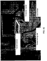
- the silicon probe was dipped into a silicon etchant after the RIE etching to test for total coating.
- the silicon was not etched after 1 minute of dipping, which validates the coating is still intact and thus full biocompatibility is achieved.
- XeF 2 was used to roughen the surface of silicon substrate to enhance the mechanical adhesion of the parylene/silicon interface.
- the depth, undercut and the shape of the resulting surface becomes hard to control. This may result in broken metal lines as well as thermal stress cracks on the border lines during the high temperature electron beam evaporation of platinum.
- the melted parylene alternative was used to enhance the adhesion of the desired area.
- Device testing was performed in three phases: in-vitro measurements in saline solution, in-vivo probe penetration testing and accelerated life testing.
- a totally biocompatible packaging/integration solution to embed amplifiers near the recording sites would be advantageous. Desirable and advantageous criteria for a well-packaged device for implantation would include avoidance of infections and inflammatory responses; the ability to withstand the harsh physiological environment of the human body (or an animal body); ease of fabrication; and as low a cost as possible.
- a new packaging technique that utilizes a flexible parylene pocket on silicon substrate with metal pads. This pocket can house an IC chip and provide electrical connections to it, and can be totally integrated with silicon probes. By application of this technology, one can make the chips and probes separately and later package them together, which is an advantage in IC/probe integration.
- FIG. 19 shows the drawing of a wireless parylene pocket integration scheme.
- the whole bonding structure is conformally coated and sealed with parylene-C (poly-para-xylylene-C), and with medical grade epoxy to achieve total encapsulation for biocompatibility.
- parylene-C poly-para-xylylene-C
- medical grade epoxy to achieve total encapsulation for biocompatibility.
- parylene pockets presented now have been designed to accommodate a 300 ⁇ m thick, 0.5 mm x 0.5 mm sized commercial IC chip.
- the parylene C cable and pocket thickness is 12 ⁇ m with gold metal connection traces embedded. It is believed that gold electrodeless plating is an alternative pad-to-pad interconnection technique.
- the two openings on two sides of this pocket were designed to provide stress relief during the insertion.
- the edge of the pocket has a 1 mm wide melted parylene adhesion layer section to provide the adhesion between the parylene and the silicon substrate.
- This structure also comprises a parylene pocket integrated with a 2-D 32 channel flexible cabled electrode array device shown in FIG. 7 ), which can be expanded to 3-D 32xN channel structures by probe stacking.
- the silicon base of the pocket is 0.8 mm x 0.8 mm in size and is 500 ⁇ m thick.
- the parylene pocket is connected to a 7 cm cable with a 60 degree Y shape pattern at the end, as illustrated in FIG. 20 .
- the silicon shank is 150 ⁇ m thick and has length of 5.1 mm, 4.6 mm, 4.1 mm and 3.6 mm from longest to shortest, respectively, as shown in FIG. 21 .
- parylene pocket structures are fabricated on double side polished wafers with DRIE (Deep Reactive Ion Etching) technology.
- FIG. 22 shows the fabrication process.
- a sacrificial photoresist layer 2206 is spin-coated for pocket releasing.
- a layer 2208 of parylene-C (6 ⁇ m) is then deposited, followed by a layer 2210 of Cr/Au (0.05/0.2 ⁇ m) lift-off process with electron beam evaporation to provide electrical connection.
- the top layer 2212 of parylene-C (6 ⁇ m) is deposited to complete the parylene-metal-parylene sandwich structure.
- Electrode sites 2214, 2214' and the device definition are then opened by a two-step RIE with O 2 Plasma (Reactive Ion Etching) process.
- the outline of the parylene pocket structure 2216 is subsequently etched by DRIE from both sides of the wafer.
- the devices are released in photoresist stripper and dried.
- the completed open pocket has at least one electrical contact configured to be accessible on an internal surface thereof, as shown in the lowest panel on the right side of FIG. 22 , in which open pocket 2216 has opening 2214 on the right through which a conductive epoxy can connect metal layer 2210 to a pad on a chip that is inserted in pocket 2216.
- similar open pockets provided by the invention also have at least one electrical contact configured to be accessible on an internal surface of the pocket.
- FIG. 24 is an illustrative example that shows a pocket in which a chip 2420 is in contact with a conductive epoxy bonding surface on one side, and situated in a pocket defined by a layer of parylene 2408, a conductive layer 2410, and a second layer parylene 2412.
- a conductive epoxy drop is placed so as to contact conductive layer 2410 and a conduction pad on the chip 2420.
- all of the electrical contacts can be made from one side of a chip 2420, or electrical contacts can be made at predefined locations on two sides of a single chip, as illustrated by the pocket structure illustrated in cross-section in FIG 35L .
- the structure can be totally coated with parylene-C again for complete encapsulation and to ensure biocompatibility.
- Device testing was performed in two phases: chip integration testing for both conduction and amplifier chips, which are illustrated in FIG. 27 , and accelerated life testing in a saline environment.
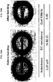
- the embedded CMOS amplifier chip used is a scalable 16-channel pre-amplifier and buffer chip with an in-band gain of 35.5 dB. This chip was tested using a function generator on a pocket only structure, as shown in FIG. 28 . Both sine waves and square waves with frequency of 0.5 kHz, 1 kHz, 2 kHz and 5 kHz and amplitude of 5 mV were passed into the chip. The amplified output, shown in FIG. 29 , from the oscilloscope concludes a successful functionality testing of our packaging technology. The conduction chip was bonded in a silicon probe integrated pocket and the impedances of the electrodes were measured.
- FIG. 30 In addition to the totally integrated silicon probe array, a second design was developed. It comprises a probe device with 36 electrodes and 2 reference electrodes separated from the parylene pocket structure, which is illustrated in FIG. 30 .
- the probe device has identical geometry as that of the totally integrated device previously described. By separating the probe structure from the parylene pocket structure, a user would be able to test the pocket structure with the integrated IC chip before connecting it to the electrodes on the silicon probe, resulting in an advantage in terms of yielding and reliable testing.
- the assembled device is shown in FIG. 31 . We use conductive epoxy as the medium for bonding the probe to the chip encapsulated in the parylene pocket.
- An important goal in neural prosthesis is to be able to decode the movement intention in the parietal cortex from neurons by implanting neuroprobes. While 3-D integrated silicon probes have been successfully manufactured, the degradation of the signal to noise ratio (SNR) is still a major challenge because electronics are too far away from the recording site. Thus, a biocompatible packaging/integration solution to embed amplifiers near the recording sites would provide an advantage.
- SNR signal to noise ratio
- This pocket can both house an IC chip inside and provide electrical connections to it, and can be integrated with silicon probes.
- the pocket size and the electrodes can be modified to suit different chips and applications as illustrated in FIG. 19 and is not sensitive to dry etching flatness.
- the whole bonding structure is conformally coated and sealed with parylene-C (poly-para-xylylene-C), and with medical grade epoxy to achieve total encapsulation for biocompatibility.
- parylene-C poly-para-xylylene-C
- medical grade epoxy to achieve total encapsulation for biocompatibility.
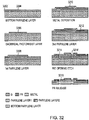
- the parylene pocket configuration is fabricated with RIE technology (Reactive Ion Etching) as illustrated in the process illustrated in FIG. 32 .
- RIE technology Reactive Ion Etching
- a bottom layer 3204 of 5 ⁇ m thick parylene-C is deposited on a silicon wafer 3202.
- a layer 3206 of sacrificial photoresist of 1 ⁇ m is then coated, which when removed will serve to define the parylene pocket structure.
- Another layer 3208 of parylene-C (5 ⁇ m) is deposited.
- a layer 3210 of Cr/Au (0.05/0.2 ⁇ m) is deposited using a lift-off process to provide electrical connection.
- the top layer 3212 of parylene-C (2 ⁇ m) is deposited to complete the structure.
- Electrode sites 3214, 3214' and the device definition are then created by a two-step RIE with O 2 Plasma process.
- the devices are released in photoresist stripper.
- An IC chip (see FIG. 27 ) is then inserted by hand into the parylene pocket, aligned (see FIG. 25 ), bonded with conductive epoxy (see FIG. 26 ) and totally coated with 10 ⁇ m of parylene.
- CMOS amplifier chip was tested using a function generator on the pocket only structure, shown in FIG. 33 . Sine and square waves of different frequencies were passed into the chip.
- the amplified output was measured and plotted, as illustrated in FIG. 29 .
- a conduction chip was then bonded with a silicon probe (see FIG. 30 ) to form an integrated pocket structure, as illustrated in FIG. 34 .
- the impedances of the probe electrodes were successfully measured, which indicates a successful functionality testing of our packaging technique.
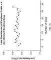
- an on-going accelerated soaking life-time test was done on the packaged structure to determine the mean-time-to-failure. Testing shows the pocket structure with 1.5 mm of epoxy is able to function after soaking in 90 °C saline for more than 30 days, which should translate to years of lifetime in saline at 37 °C.
- FIG. 35 is a diagram showing the steps performed in fabricating a self supporting parylene pocket structure that provides contacts to chips having contact pads on two opposite surfaces. This capability will allow the use of chips that are expected to have greater functionality as compared to chips having contacts on only one surface.
- a silicon wafer 3502 having a polished surface is provided as a support structure.
- a first layer of parylene 3504 is applied to the deposited on selected areas of the parylene layer 3504.
- the first metal layer 3506 may comprise more than one metal structure, such as parallel lines configured to provide conductor traces and/or multiple connector pads. As illustrated in FIG.
- a second layer of parylene 3508 is deposited to cover and encapsulate the first metal layer 3506.
- the second layer of parylene 3508 can extend to a substantially similar extent as the first parylene layer 3504.
- an opening 3510 is created (for example by etching) in the second parylene layer 3508 to provide a path to make contact to a contact pad in the first metal layer 3506.
- a layer of photoresist 3512 is provided that covers the opening 3510 and that represents a sacrificial volume that when opened, provides a space into which a chip may be inserted.
- FIG. 35D a second layer of parylene 3508 is deposited to cover and encapsulate the first metal layer 3506.
- the second layer of parylene 3508 can extend to a substantially similar extent as the first parylene layer 3504.
- an opening 3510 is created (for example by etching) in the second parylene layer 3508 to provide a path to make contact to a contact pad in the first metal layer 3506.
- a third parylene layer 3514 is provided over the photoresist layer 3512.
- the third parylene layer 3514 can extend to a substantially similar extent as the first parylene layer 3504.
- a second layer of metal 3516 is deposited on selected areas of the third parylene layer 3514.
- the second metal layer 3514 may comprise more than one metal structure, such as parallel lines configured to provide conductor traces and/or multiple connector pads.
- a fourth parylene layer 3518 is deposited to cover and encapsulate the second metal layer 3516.
- the fourth parylene layer 3518 can extend to a substantially similar extent as the first parylene layer 3504. As illustrated in FIG.
- openings 3520 are provided to allow access to the contact pads in the second metal layer 3516.
- the openings are created using reactive ion etching (RIE) methods.
- RIE reactive ion etching
- openings 3522, 3522' are etched through the structure to allow electrical access to all of the contact pads.
- the self supporting parylene pocket structure is released from the silicon wafer 3502 and the sacrificial layer of photoresist 3512 is removed, leaving a free-standing self supporting parylene pocket structure having metal contacts and leads that can be connected to contact pads on two opposite sides of a chip, such as an IC chip or a chip having desired electronic, computational, or other capabilities.
- the leads in the parylene pocket can be used to make electrical connection to circuitry, probes, or other electrical or electronic devices that allow communication with the encapsulated chip.
- the system comprises a CMOS stimulator chip, a fold-and-bond RF coil, two platinum electrodes, and discrete capacitors.
- the MEMS components are fabricated with a parylene-metal skin technology, and the system assembly is achieved by interconnecting individual components together on a parylene substrate with silver epoxy.
- the functionality of the integrated system has been verified using a telemetry link setup, and single-phase pulses with amplitudes ranging from 7 to 8.5 V have been detected.
- a parylene-metal skin technology allows us to microfabricate RF coils and multielectrode arrays in a process compatible way.
- MEMS devices are fabricated separately, and assembled with other system components using biocompatible silver epoxy.
- Parylene-C serves as a substrate and packaging material, and therefore the final system is highly flexible and biocompatible for medical implantation.
- FIG. 36A depicts the system schematic of a single channel stimulator, which comprises a BION1-3 CMOS chip, two capacitors, a specially designed RF MEMS coil for wireless power and data transmission from an external personal trainer, as well as a carrier substrate.
- the flexible carrier has interconnection leads and contact pads for system assembly, and two electrodes of which one serves as the stimulating electrode while the other is the floating ground.
- the overall physical dimensions of the MEMS coil and the carrier substrate are to meet specifications used in retinal implantation, which are determined based on surgical implantation results in canine eyes.
- the BION chip is a single-channel stimulator which is initially developed to mimic muscle spindle function, and to treat patients suffering from muscle paralysis. Once implanted into paralyzed muscles, the chip can receive both power and command signals through inductive coupling over a 480 kHz ⁇ 500 kHz power carrier generated in an external unit, allowing the chip to emit precisely timed stimulation pulses with highly regulated amplitude and pulse-width.
- the BION chip has physical dimensions of ⁇ 1 mm in width, ⁇ 2.33 mm in length, and ⁇ 257 ⁇ m in thickness. There are five pads on the chip with sizes of approximately 120 ⁇ m ⁇ 74 ⁇ m. The distance between two adjacent pads is about 110 ⁇ m.
- C 1 is a frequency tuning capacitor in parallel with the receiving coil to achieve a resonant frequency of ⁇ 500 kHz.
- C 2 is a charge storage capacitor which has a capacitance of ⁇ 22 nF, provided by Dr. Gerald Loeb's group at the University of Southern California. These capacitors are about 1 mm ⁇ 0.5 mm ⁇ 0.56 mm in size.
- the fabrication is divided into three steps: carrier substrate fabrication, RF MEMS coil fabrication, and final system assembly and packaging.
- carrier substrate fabrication a 200 nm layer of platinum is e-beam evaporated on a parylene-C coated silicon substrate.
- the metal is patterned using lift-off to form connection pads, interconnection leads, and electrode sites. Platinum is selected as the electrode material for optimal simulation capability. No adhesion metal layer is need in this case because platinum and parylene are known to have good mutual adhesion.
- FIG. 37 illustrates the detailed process for making the carrier substrate, where steps 37B through 37D describe the lift-off technology for platinum patterning.
- a polished silicon wafer 3702 has a layer of parylene 3704 deposited thereon.
- layers of a LOR3B resist 3706 and a regular photoresist 3708 are deposited and patterned.
- a metal 3710 is deposited over the patterned resists.
- Fig. 37D the resists are removed, leaving metal 3710 in predefined locations on the parylene layer 3704.
- additional parylene is deposited.
- FIG. 37F the separated substrate is illustrated.
- FIG. 38 presents a fabricated carrier substrate.
- the microscope image shows a special chip site design where parylene ribbons are etched in a way such that the chip can be held in place and self-aligned to the contact vias on the substrate during system assembly.
- the array site contains a 450 ⁇ m diameter tack hole so that the array can be attached to the retina using a retinal tack.
- a fold-and-bond technology is involved, in which two coils are placed in series, and made of a single 3 ⁇ m layer of gold to achieve low resistance and high Q factor. Then the device is folded into two layers and stacked together with the assistance of two glass slides. Aluminum sheets are inserted between the parylene surface and the class slides to prevent parylene sticking on the glass. After that, the stacked coil is placed in a vacuum oven with a chamber pressure of ⁇ 10 Torr for bonding. The oven temperature ramps from room temperature to 250°C. The device is then soaked at the bonding temperature for 2 days, followed by a slow cool-down to room temperature. Nitrogen backfill is introduced during the thermal bonding process to equalize the chamber temperature.
- FIG. 39 A fabricated coil is shown in FIG. 39 , comprising two layers of metal with 10 turns in each layer.
- In-and-out leads are connected to the carrier substrate from the center, facilitating the surgical procedure.
- Through vias are designed to overlap with the contact pads, so that the interconnections to the carrier substrate can be formed from either side.
- the electrical properties of this coil are measured, showing an inductance of approximately 2.24 ⁇ H and a DC resistance of approximately 15.82 ⁇ , which results in a Q factor of 0.45 at 500 kHz.
- FIG. 40 illustrates an assembled single channel stimulator system.
- FIG, 41 shows close-up views on the interconnections for each component.
- FIG. 43 which comprises a personal trainer unit, a class-E coil driver and a hand-wound transmitting coil, can generate a power carrier of approximately 500 kHz.
- the personal trainer stores command programs personalized for individual subjects, records the time and duration of treatment, and transfers this information to an external computer for real time monitoring. Up to three programs can be preloaded into the memory of the personal trainer.
- the coil driver is connected to the personal trainer through a custom made adapter.
- the transmitting coil has an inductance of ⁇ 46.4 ⁇ H and a Q factor of ⁇ 118 at 500 kHz.
- Litz wires 1025-44 SPN are used for winding the primary coil to reduce the skin effect and proximity effect losses.
- the transmitting coil is built in a solenoid shape to establish a more uniform electromagnetic field inside the coil. Additionally, ferrite cores are inserted in the transmitting coil to magnify the electromagnetic field and therefore to improve voltage transfer efficiency.
- FIG. 45 shows typical waveforms of the transferred voltage and current, indicating a resonant frequency of ⁇ 505 kHz and a -25 degree phase drift between voltage and current.
- the tuning capacitor is a commercially available chip capacitor, which has limited options of capacitance values. Therefore, it is difficult to fine tune the resonant circuit to achieve precise synchronization.
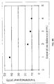
- the delivered power at the different separation distances are also investigated, as shown in FIG. 46 .
- the MEMS coil can transfer a maximum power of ⁇ 43 mW through this inductive link at the separation distance of 1 mm. As the separation distance increases to 2 mm, the power drops by 62%, which is mainly limited by the low Q factor of the receiving coil.
- a single channel neural stimulator has been designed, and one embodiment has been successfully fabricated and tested. Test results demonstrate that the BION chip can be driven by the MEMS coil within a 4 mm separation distance. Output pulses with a pulse width of ⁇ 500 ⁇ s and amplitudes of more than 7 V are measured from the simulating electrode, indicating that system can be operated in vitro.
- the parylene pocket structure is fabricated with a combination of RIE (Reactive Ion Etching) and DRIE (Deep Reactive Ion Etching) processes.
- a sacrificial photoresist layer 4706 is spin-coated for pocket releasing.
- a layer 4708 of parylene-C (6 ⁇ m) is then deposited, followed by a layer 4710 of Cr/Au (0.05/0.2 ⁇ m) lift-off process with electron beam evaporation to provide electrical connection.
- the top layer 4712 of parylene-C (6 ⁇ m) is deposited to complete the parylene-metal-parylene sandwich structure.
- Electrode sites 4714, 4714' and the device definition are then opened by a two-step RIE with O 2 Plasma (Reactive Ion Etching) process.
- a DRIE backside etch is used to define the back surface dimensions as defined by etched trenches 4720 and 4720'.
- the parylene pocket structure 4716 is opened in photoresist stripper and the structure is dried.
- An IC chip is then inserted into the parylene pocket as illustrated in FIG. 48 . It is aligned with the traces in the pocket as shown in FIG. 49 and FIG. 50 .
- the chip is bonded with conductive epoxy as illustrated in FIG. 51 .
- the structure can be totally coated with parylene-C again for complete encapsulation and to ensure biocompatibility.
- an 1C chip is then inserted into the parylene pocket, in some embodiments by hand, aligned as shown in FIG. 49 and FIG.50 , and bonded with a conductive epoxy squeegee process, as shown in FIG. 51 . It is then totally coated with parylene for overall biocompatibility.
- epoxy squeegee process a commercially available conductive epoxy is mixed and applied globally on the surface of the chip. A rubber squeegee is then used to push excess epoxy off the target surface of the chip pad bonding area. Pulsed laser annealing with an ultra-violet laser is then utilized to cure the epoxy connections locally, which enhances the physical strength and stiffness of the bond.
- acetone is used to wash away the uncured conductive epoxy, which leaves the surface of the bonding pad relatively clean and the space between pads free of unwanted short circuit conductions, as shown in FIG. 52 and FIG. 53 .
- the profile of the bonding epoxy bumps has been examined. The result illustrated in FIG. 54 shows that the maximum height is ⁇ 25 ⁇ m.
- discrete components such as diodes and capacitors can be connected to this parylene-pocket structure.
- Device testing is performed in two stages.
- the first stage is chip integration testing and the second stage accelerated life testing.
- a dummy chip with dimensions of 5 mm x 5 mm x 500 ⁇ m is inserted into the pocket and bonded with the laser annealing technique to test the functionality of the structure.
- the pads on the dummy chip have minimum distances of 140 ⁇ m and maximum distances of 500 ⁇ m.
- Commercial discrete components such as capacitors, resistors and inductors (coils) are connected to the pads on the parylene layer and are tested with a function generator. Sine waves of different frequency were passed into the chip and the components.
- FIG. 56 illustrates the successful functionality testing of the packaging technology.
- accelerated life-time soaking test is conducted to determine the mean-time-to-failure of the devices. Testing shows the pocket structure with 1.5 mm of biocompatible silicone is able to function after soaking in 90 °C saline for more than 30 days, which should translate to years of lifetime in saline at 37 °C.
- pockets may be most suitable for different applications. Examples include a pocket on a silicon substrate; an all-parylene pocket; pockets designed to encapsulate specific commercially available chips; pockets designed to encapsulate discrete components; pockets designed to encapsulate PCBs; a single layer pocket; a double layer pocket; a multi layer pocket; pocket stacking to achieve a 3D structure; a pocket with parylene cable connected thereto; a pocket with a MEMS coil; a pocket with MEMS capacitors and pockets comprising materials other than parylene.
- Interconnection has been demonstrated using several procedures, including the squeegee method; the hand paint method; methods involving use of conductive epoxy; and a laser annealing method, in which laser-assisted annealing and curing of the conductive epoxy/polymer has been successfully demonstrated.
- Recording the results from a data collection operation e.g., obtaining and recording a signal representing data or information, or obtaining and recording an image, such as for example, recording results in one or more dimensions, using one or more colors or hues, or at a particular frequency or wavelength, is understood to mean and is defined herein as writing output data to a storage element, to a machine-readable storage medium, or to a storage device.
- the recorded information can be analog information and/or digital information, as a particular embodiment may suggest or require.
- Machine-readable storage media that can be used in the invention include electronic, magnetic and/or optical storage media, such as magnetic floppy disks and hard disks; a DVD drive, a CD drive that in some embodiments can employ DVD disks, any of CD-ROM disks (i.e., read-only optical storage disks), CD-R disks (i.e., write-once, read-many optical storage disks), and CD-RW disks (i.e., rewriteable optical storage disks); and electronic storage media, such as RAM, ROM, EPROM, Compact Flash cards, PCMCIA cards, or alternatively SD or SDIO memory; and the electronic components (e.g., floppy disk drive, DVD drive, CD/CD-R/CD-RW drive, or Compact Flash/PCMCIA/SD adapter) that accommodate and read from and/or write to the storage media.
- DVD drive a CD drive that in some embodiments can employ DVD disks, any of CD-ROM disks (i.e., read-only optical storage disks), CD
- Recording image data for later use can be performed to enable the use of the recorded information as output, as data for display to a user, or as data to be made available for later use.
- Such digital memory elements or chips can be standalone memory devices, or can be incorporated within a device of interest.
- Writing output data or "writing an image to memory” is defined herein as including writing transformed data to registers within a microcomputer.
- image can be understood to mean either a "picture,” whether visible to a human observer or to an instrument (e.g., a visible image, an infrared image, or a digital representation of such an image, whether in black and white or in color), or alternatively, a "copy”, as in “an image of a hard disk,” whether a duplicate copy, a compressed copy, or an encrypted copy.
- Microcomputer is defined herein as synonymous with microprocessor, microcontroller, and digital signal processor (“DSP”). It is understood that memory used by the microcomputer, including for example an imaging or image processing algorithm coded as “firmware” can reside in memory physically inside of a microcomputer chip or in memory external to the microcomputer or in a combination of internal and external memory. Similarly, analog signals can be digitized by a standalone analog to digital converter (“ADC”) or one or more ADCs or multiplexed ADC channels can reside within a microcomputer package. It is also understood that field programmable array (“FPGA”) chips or application specific integrated circuits (“ASIC”) chips can perform microcomputer functions, either in hardware logic, software emulation of a microcomputer, or by a combination of the two. Apparatus having any of the inventive features described herein can operate entirely on one microcomputer or can include more than one microcomputer.
- ADC analog to digital converter
- FPGA field programmable array
- ASIC application specific integrated circuits
- General purpose programmable computers useful for controlling instrumentation, recording signals and analyzing signals or data according to the present description can be any of a personal computer (PC), a microprocessor based computer, a portable computer, or other type of processing device.
- the general purpose programmable computer typically comprises a central processing unit, a storage or memory unit that can record and read information and programs using machine-readable storage media, a communication terminal such as a wired communication device or a wireless communication device, an output device such as a display terminal, and an input device such as a keyboard.
- the display terminal can be a touch screen display, in which case it can function as both a display device and an input device.
- Different and/or additional input devices can be present such as a pointing device, such as a mouse or a joystick, and different or additional output devices can be present such as an enunciator, for example a speaker, a second display, or a printer.
- the computer can run any one of a variety of operating systems, such as for example, any one of several versions of Windows, or of MacOS, or of UNIX, or of Linux. Computational results obtained in the operation of the general purpose computer can be stored for later use, and/or can be displayed to a user. At the very least, each microprocessor-based general purpose computer has registers that store the results of each computational step within the microprocessor, which results are then commonly stored in cache memory for later use.
Landscapes
- Health & Medical Sciences (AREA)
- Life Sciences & Earth Sciences (AREA)
- Engineering & Computer Science (AREA)
- Public Health (AREA)
- Biomedical Technology (AREA)
- Veterinary Medicine (AREA)
- Animal Behavior & Ethology (AREA)
- General Health & Medical Sciences (AREA)
- Medical Informatics (AREA)
- Physics & Mathematics (AREA)
- Biophysics (AREA)
- Pathology (AREA)
- Heart & Thoracic Surgery (AREA)
- Molecular Biology (AREA)
- Surgery (AREA)
- Radiology & Medical Imaging (AREA)
- Computer Networks & Wireless Communication (AREA)
- Nuclear Medicine, Radiotherapy & Molecular Imaging (AREA)
- Prostheses (AREA)
- Electrotherapy Devices (AREA)
Claims (8)
- Biokompatible Tasche, welche konfiguriert ist, um eine Elektrische-Schaltung-Komponente aufzunehmen, und konfiguriert ist, um versiegelt zu werden und innerhalb eines lebenden Organismus implantiert zu werden, nach dem Aufnehmen der besagten Elektrische-Schaltung-Komponente,
aufweisend:ein biokompatibles Silizium-Substrat, wobei das biokompatible Silizium-Substrat eine erste Fläche aufweist, undeine erste Schicht aus Parylen (2208), welche mit der besagten Fläche des besagten Substrats verbunden ist, wobei die besagte Schicht eine Taschenstruktur (2216) zwischen dem besagten Substrat und der besagten Schicht definiert,eine Metallschicht (2210) an der besagten ersten Schicht aus Parylen (2208),eine zweite Schicht aus Parylen (2212) an der besagten Metallschicht (2210),eine erste Öffnung (2214), welche sich durch die besagte erste Schicht aus Parylen (2208) und durch die besagte zweite Schicht aus Parylen (2212) hindurch erstreckt, wodurch es einem leitfähigen Epoxidharz ermöglicht wird, die besagte Metallschicht (2210) mit einem Pad an einer Elektrische-Schaltung-Komponente zu verbinden, wenn die besagte Elektrische-Schaltung-Komponente in die besagte Tasche eingebracht ist, wobei die besagte Tasche dadurch einen elektrischen Kontakt aufweist, welcher konfiguriert ist, um an einer Innenfläche davon zugänglich zu sein, wobei die besagte biokompatible versiegelbare Tasche konfiguriert ist, um mit Epoxid versiegelt zu werden. - Biokompatible versiegelbare Tasche gemäß Anspruch 1, welche ferner ein elektrisches Kabel aufweist, welches elektrische Leiter darin aufweist, welche konfiguriert sind, um eine elektrische Verbindung zwischen mindestens einem Sondenelement und der besagten mindestens einen Elektrische-Schaltung-Komponente, welche sich innerhalb der besagten Tasche befindet, herzustellen, wobei das besagte Sondenelement konfiguriert ist, um eine elektrische Verbindung zu dem lebenden Organismus herzustellen, wenn die besagte biokompatible Tasche in den lebenden Organismus implantiert ist.
- Biokompatible versiegelbare Tasche gemäß Anspruch 1, ferner aufweisend:
eine Elektrisches-Signal-Kommunikation-Vorrichtung, welche ein Kabel aufweist, welches konfiguriert ist, um eine elektromagnetische Verbindung zwischen der besagten mindestens einen Elektrische-Schaltung-Komponente und einer Elektrische-Schaltung-Vorrichtung, welche sich außerhalb des besagten lebenden Organismus befindet, herzustellen. - Biokompatible versiegelbare Tasche gemäß Anspruch 1 in Kombination mit:mindestens einer Elektrische-Schaltung-Komponente, welche sich innerhalb der besagten Tasche befindet und elektrisch mit der besagten mindestens einen Elektrische-Verbindung-Vorrichtung verbunden ist,mindestens einer Sonde, welche konfiguriert ist, um eine elektrische Verbindung zu einem lebenden Organismus herzustellen, und mit der besagten mindestens einen Elektrische-Schaltung-Komponente verbunden ist, undeiner Elektrische-Kommunikation-Vorrichtung, welche konfiguriert ist, um ein elektrisches Signal zwischen der besagten mindestens einen Elektrische-Schaltung-Komponente und einer Elektrische-Schaltung-Vorrichtung, welche sich außerhalb des lebenden Organismus befindet, zu übermitteln.
- Verfahren zum Herstellen einer biokompatiblen versiegelbaren Tasche, welches die folgenden Schritte aufweist:12a. Bereitstellen eines biokompatiblen Silizium-Substrats oder eines biokompatiblen Polymermaterial-Substrats, wobei das Substrat eine erste Fläche aufweist,12b. Abscheiden einer Schicht aus einem Opfermaterial, welche eine vordefinierten Länge, eine vordefinierte Breite und eine vordefinierte Dicke hat, an einem Abschnitt der besagten Fläche des besagten biokompatiblen Substrats,12c. Abscheiden einer Schicht aus dem besagten biokompatiblen Polymermaterial über der besagten Schicht aus dem besagten Opfermaterial, wobei die besagte Schicht aus dem besagten biokompatiblen Polymermaterial sich über das besagte Opfermaterial hinaus erstreckt,12d. Abscheiden einer Schicht aus einem leitfähigen Material über mindestens einem Abschnitt der besagten Schicht aus dem besagten biokompatiblen Polymermaterial,12e. Abscheiden einer zweiten Schicht aus einem biokompatiblen Polymermaterial über der besagten Schicht aus dem besagten leitfähigen Material, wobei die besagte Schicht aus dem besagten biokompatiblen Material sich über das besagte leitfähige Material hinaus erstreckt,12f. Bereitstellen von Öffnungen in der besagten zweiten Schicht aus dem besagten biokompatiblen Polymermaterial, um einen elektrischen Zugang zu dem besagten leitfähigen Material durch die besagte zweite Schicht aus dem besagten biokompatiblen Polymermaterial hindurch bereitzustellen, und12g. Entfernen des besagten Opfermaterials, um ein freies Volumen zu definieren, welches die besagte vordefinierte Länge, die besagte vordefinierte Breite und die besagte vordefinierte Dicke hat, wobei das besagte freie Volumen konfiguriert ist, um mindestens eine Elektrische-Schaltung-Komponente aufzunehmen,wodurch das besagte freie Volumen eine offene Tasche darstellt, welche mindestens einen elektrischen Kontakt hat, welcher konfiguriert ist, um an einer Innenfläche davon zugänglich zu sein,
wobei die besagte offene Tasche konfiguriert ist, um mindestens eine Elektrische-Schaltung-Komponente aufzunehmen und eine elektrische Kommunikation zwischen dem mindestens einen elektrischen Kontakt und der besagten mindestens einen Elektrische-Schaltung-Komponente bereitzustellen,
wobei die besagte biokompatible versiegelbare Tasche konfiguriert ist, um versiegelt zu werden und innerhalb eines lebenden Organismus implantiert zu werden nach dem Aufnehmen der besagten mindestens einen Elektrische-Schaltung-Komponente,
wobei die besagte biokompatible versiegelbare Tasche konfiguriert ist, um ein biokompatibles Objekt bereitzustellen, welches zu einer biologisch signifikanten elektrischen Kommunikation mit dem besagten lebenden Organismus in der Lage ist, innerhalb dessen die besagte biokompatible versiegelbare Tasche implantiert ist. - Verfahren zum Herstellen einer biokompatiblen versiegelbaren Tasche gemäß Anspruch 5, welches ferner die folgenden Schritte aufweist:nach dem Schritt 12a. des Bereitstellens eines biokompatiblen Substrats, und vor dem Schritt 12b. des Abscheidens einer Schicht eines Opfermaterials,
13(i) Abscheiden an der besagten Fläche des besagten biokompatiblen Substrats einer Schicht aus dem besagten biokompatiblen Polymermaterial, wobei die besagte Schicht aus dem besagten biokompatiblen Polymermaterial eine Länge aufweist, welche größer als die besagte vordefinierte Länge des besagten Opfermaterials ist, und wobei die Schicht aus dem besagten biokompatiblen Polymermaterial eine Breite aufweist, welche größer als die besagte vordefinierte Breite des besagten Opfermaterials ist,wodurch das besagte freie Volumen eine offene Tasche darstellt, welche das besagte biokompatible Polymermaterial als jede seiner definierenden Flächen aufweist. - Verfahren zum Herstellen einer biokompatiblen versiegelbaren Tasche gemäß Anspruch 6, ferner den folgenden Schritt aufweisend:
Ablösen der besagten biokompatiblen versiegelbaren Tasche von dem besagten biokompatiblen Substrat, um eine selbsttragende freistehende biokompatible versiegelbare Tasche bereitzustellen. - Verfahren zum Herstellen einer biokompatiblen versiegelbaren Tasche gemäß Anspruch 6, ferner die folgenden Schritte aufweisend:nach dem Schritt 13(i) des Abscheidens an der besagten Fläche des besagten biokompatiblen Substrats einer Schicht aus dem besagten biokompatiblen Polymermaterial, und vor dem Schritt 12b. des Abscheidens einer Schicht aus einem Opfermaterial,15(ii) Abscheiden einer Schicht aus einem leitfähigen Material über mindestens einem Abschnitt der besagten Schicht aus dem besagten biokompatiblen Polymermaterial,15(iii) Abscheiden einer Schicht aus dem besagten biokompatiblen Polymermaterial über der besagten Schicht aus dem besagten leitfähigen Material, wobei sich die besagte Schicht aus dem besagten biokompatiblen Polymermaterial über das besagte leitfähige Material hinaus erstreckt, und15(iv) Bereitstellen von Öffnungen in der besagten Schicht aus dem besagten biokompatiblen Polymermaterial, welches in Schritt 15(iii) abgeschieden wurde, um einen elektrischen Zugang zu dem besagten leitfähigen Material durch die besagte Schicht aus dem besagten biokompatiblen Polymermaterial hindurch bereitzustellen, welches in Schritt 15(iii) abgeschieden wurde,
und nach dem Schritt 12f. des Bereitstellens von Öffnungen, und vor dem Schritt 12g. des Entfernens des besagten Opfermaterials,15(v) Bereitstellen von Öffnungen in den besagten Schichten, welche in den Schritten 15(iii), 12b, 12c, 12d und 12e abgeschieden wurden, um einen elektrischen Zugang zu dem besagten leitfähigen Material, welches in Schritt 15(ii) abgeschieden wurde, durch die besagte Schicht des besagten biokompatiblen Materials hindurch bereitzustellen, welches in Schritt 15(iii) abgeschieden wurde,wodurch eine biokompatible versiegelbare Tasche bereitgestellt wird, welche elektrische Kontakte an zwei Innenflächen davon hat.
Applications Claiming Priority (2)
| Application Number | Priority Date | Filing Date | Title |
|---|---|---|---|
| US20549009P | 2009-01-21 | 2009-01-21 | |
| PCT/US2010/000171 WO2010090706A2 (en) | 2009-01-21 | 2010-01-21 | Pocket-enabled chip assembly for implantable devices |
Publications (3)
| Publication Number | Publication Date |
|---|---|
| EP2389101A2 EP2389101A2 (de) | 2011-11-30 |
| EP2389101A4 EP2389101A4 (de) | 2013-06-19 |
| EP2389101B1 true EP2389101B1 (de) | 2020-11-18 |
Family
ID=42542567
Family Applications (1)
| Application Number | Title | Priority Date | Filing Date |
|---|---|---|---|
| EP10738838.1A Active EP2389101B1 (de) | 2009-01-21 | 2010-01-21 | Taschenaktivierte chipanordnung für implantierbare vorrichtungen |
Country Status (4)
| Country | Link |
|---|---|
| US (1) | US8824156B2 (de) |
| EP (1) | EP2389101B1 (de) |
| CN (1) | CN102355854B (de) |
| WO (1) | WO2010090706A2 (de) |
Families Citing this family (31)
| Publication number | Priority date | Publication date | Assignee | Title |
|---|---|---|---|---|
| FR2957523B1 (fr) * | 2010-03-18 | 2012-04-27 | Dixi Microtechniques | Procede de fabrication d'une electrode a usage medical et electrode obtenue par la mise en oeuvre de ce procede |
| ITRM20110206A1 (it) | 2011-04-21 | 2012-10-22 | Ab Medica Spa | Sistema di acquisizione e monitoraggio di segnali bioelettrici provenienti dal cervello e di stimolazione intracranica. |
| US20130041704A1 (en) * | 2011-08-11 | 2013-02-14 | Bank Of America Corporation | Initiative consolidation management |
| US10008443B2 (en) * | 2012-04-30 | 2018-06-26 | California Institute Of Technology | Implant device |
| WO2013165599A1 (en) * | 2012-04-30 | 2013-11-07 | California Institute Of Technology | High-lead count implant device and method of making the same |
| US9224664B2 (en) | 2012-06-06 | 2015-12-29 | The Charles Stark Draper Laboratory, Inc. | Bio-implantable hermetic integrated ultra high density device |
| AU2013294699A1 (en) | 2012-07-26 | 2015-02-26 | Mashiachi, Adi | Internal resonance matching between an implanted device and an external device |
| CN104582635B (zh) * | 2012-08-22 | 2017-06-20 | 加州理工学院 | 用于眼植入体的3线圈的无线功率传输系统 |
| US9181086B1 (en) | 2012-10-01 | 2015-11-10 | The Research Foundation For The State University Of New York | Hinged MEMS diaphragm and method of manufacture therof |
| US9161712B2 (en) | 2013-03-26 | 2015-10-20 | Google Inc. | Systems and methods for encapsulating electronics in a mountable device |
| US9113829B2 (en) | 2013-03-27 | 2015-08-25 | Google Inc. | Systems and methods for encapsulating electronics in a mountable device |
| US20140371560A1 (en) | 2013-06-14 | 2014-12-18 | Google Inc. | Body-Mountable Devices and Methods for Embedding a Structure in a Body-Mountable Device |
| US9685689B1 (en) | 2013-06-27 | 2017-06-20 | Verily Life Sciences Llc | Fabrication methods for bio-compatible devices |
| US9028772B2 (en) | 2013-06-28 | 2015-05-12 | Google Inc. | Methods for forming a channel through a polymer layer using one or more photoresist layers |
| US9307901B1 (en) | 2013-06-28 | 2016-04-12 | Verily Life Sciences Llc | Methods for leaving a channel in a polymer layer using a cross-linked polymer plug |
| US9781842B2 (en) * | 2013-08-05 | 2017-10-03 | California Institute Of Technology | Long-term packaging for the protection of implant electronics |
| US9282920B2 (en) | 2013-08-27 | 2016-03-15 | Verily Life Sciences Llc | Sacrificial layers for bio-compatible devices |
| WO2015041944A1 (en) * | 2013-09-17 | 2015-03-26 | California Institute Of Technology | Multi-layer packaging scheme for implant electronics |
| EP2870980B1 (de) | 2013-11-08 | 2018-08-08 | NeuroNexus Technologies, Inc. | Dreidimensionale Nervensondenmikroelektrodenanordnung und Verfahren zur Herstellung |
| US9044200B1 (en) | 2013-12-17 | 2015-06-02 | Google Inc. | Noble metal surface treatment to improve adhesion in bio-compatible devices |
| US9993185B2 (en) | 2014-02-12 | 2018-06-12 | California Institute Of Technology | Plasmonics nanostructures for multiplexing implantable sensors |
| WO2015123461A1 (en) * | 2014-02-12 | 2015-08-20 | California Institute Of Technology | Reflowed gold nanostructures for surface enhanced raman spectroscopy |
| WO2016036410A1 (en) | 2014-09-05 | 2016-03-10 | California Institute Of Technology | Multiplexed surface enhanced raman sensors for early disease detection and in-situ bacterial monitoring |
| WO2016036409A1 (en) | 2014-09-05 | 2016-03-10 | California Institute Of Technology | Surface enhanced raman spectroscopy detection of gases, particles and liquids through nanopillar structures |
| US9512000B2 (en) | 2014-12-09 | 2016-12-06 | California Institute Of Technology | Fabrication and self-aligned local functionalization of nanocups and various plasmonic nanostructures on flexible substrates for implantable and sensing applications |
| US11090482B2 (en) * | 2015-06-03 | 2021-08-17 | Vomaris Innovations, Inc. | Method and devices for treating muscles |
| AU2019352954B2 (en) | 2018-10-01 | 2022-03-10 | Biovisics Medical, Inc. | System and methods for controlled electrical modulation for vision therapy |
| WO2020112980A2 (en) | 2018-11-30 | 2020-06-04 | Biovisics Medical, Llc | Head worn apparatuses for vision therapy |
| WO2020210471A1 (en) | 2019-04-10 | 2020-10-15 | Biovisics Medical, Inc. | Systems and interfaces for ocular therapy |
| WO2020252278A1 (en) | 2019-06-14 | 2020-12-17 | Biovisics Medical, Inc. | Wearable medical device |
| CN110772251B (zh) * | 2019-10-28 | 2020-11-17 | 浙江大学 | 一种软性双面神经探针及其制备方法 |
Family Cites Families (16)
| Publication number | Priority date | Publication date | Assignee | Title |
|---|---|---|---|---|
| EP0534782A1 (de) * | 1991-09-26 | 1993-03-31 | Medtronic, Inc. | Gehäuse für implantierbare medizinische Vorrichtung |
| US5741313A (en) * | 1996-09-09 | 1998-04-21 | Pacesetter, Inc. | Implantable medical device with a reduced volumetric configuration and improved shock stabilization |
| US6516808B2 (en) * | 1997-09-12 | 2003-02-11 | Alfred E. Mann Foundation For Scientific Research | Hermetic feedthrough for an implantable device |
| US8133698B2 (en) * | 2000-05-15 | 2012-03-13 | Silver James H | Sensors for detecting substances indicative of stroke, ischemia, infection or inflammation |
| US7127286B2 (en) * | 2001-02-28 | 2006-10-24 | Second Sight Medical Products, Inc. | Implantable device using ultra-nanocrystalline diamond |
| IL145700A0 (en) * | 2001-09-30 | 2002-06-30 | Younis Imad | Electrode system for neural applications |
| US7211103B2 (en) * | 2002-04-11 | 2007-05-01 | Second Sight Medical Products, Inc. | Biocompatible bonding method and electronics package suitable for implantation |
| US7190051B2 (en) * | 2003-01-17 | 2007-03-13 | Second Sight Medical Products, Inc. | Chip level hermetic and biocompatible electronics package using SOI wafers |
| US7338836B2 (en) * | 2003-11-05 | 2008-03-04 | California Institute Of Technology | Method for integrating pre-fabricated chip structures into functional electronic systems |
| US20090198293A1 (en) * | 2003-12-19 | 2009-08-06 | Lawrence Cauller | Microtransponder Array for Implant |
| EP1723983B1 (de) * | 2005-05-20 | 2013-07-10 | Imec | Sonde für die elektrische Stimulation und Bestimmung der Aktivität von erregbaren Zellen |
| EP1949437B2 (de) * | 2005-11-02 | 2021-08-04 | Second Sight Medical Products, Inc. | Implantierbare mikroelektronische vorrichtung und herstellungsverfahren dafür |
| WO2007089738A2 (en) * | 2006-01-26 | 2007-08-09 | The Regents Of The University Of Michigan | Microelectrode with laterally extending platform for reduction of tissue encapsulation |
| EP2061549B1 (de) * | 2006-08-18 | 2014-04-09 | Second Sight Medical Products, Inc. | Verpackung für eine implantierbare nervenstimulationsvorrichtung |
| US8561292B2 (en) * | 2008-11-14 | 2013-10-22 | The Regents Of The University Of Michigan | Method for manufacturing an implantable electronic device |
| EP2416841B1 (de) * | 2009-04-08 | 2015-09-23 | Saluda Medical Pty Limited | Elektronik-paket für eine wirksame implantierbare medizinische vorrichtung |
-
2010
- 2010-01-21 CN CN201080012327.0A patent/CN102355854B/zh active Active
- 2010-01-21 US US12/657,539 patent/US8824156B2/en active Active
- 2010-01-21 EP EP10738838.1A patent/EP2389101B1/de active Active
- 2010-01-21 WO PCT/US2010/000171 patent/WO2010090706A2/en active Application Filing
Non-Patent Citations (1)
| Title |
|---|
| None * |
Also Published As
| Publication number | Publication date |
|---|---|
| EP2389101A4 (de) | 2013-06-19 |
| US8824156B2 (en) | 2014-09-02 |
| US20100265680A1 (en) | 2010-10-21 |
| EP2389101A2 (de) | 2011-11-30 |
| WO2010090706A3 (en) | 2010-10-21 |
| CN102355854B (zh) | 2015-04-01 |
| WO2010090706A2 (en) | 2010-08-12 |
| CN102355854A (zh) | 2012-02-15 |
Similar Documents
| Publication | Publication Date | Title |
|---|---|---|
| EP2389101B1 (de) | Taschenaktivierte chipanordnung für implantierbare vorrichtungen | |
| US11123548B2 (en) | Microfabricated neurostimulation device | |
| US9604055B2 (en) | Microfabricated surface neurostimulation device and methods of making and using the same | |
| Wise et al. | Wireless implantable microsystems: high-density electronic interfaces to the nervous system | |
| Stieglitz | Manufacturing, assembling and packaging of miniaturized neural implants | |
| JP2017525545A (ja) | リードレス神経刺激装置 | |
| Wise et al. | Fully-implantable auditory prostheses: Restoring hearing to the profoundly deaf | |
| Li et al. | Integrated wireless neurostimulator | |
| Stieglitz | Manufacturing, assembling and packaging of miniaturized implants for neural prostheses and brain-machine interfaces | |
| Koch et al. | Polymer-based implantable electrodes: state of the art and future prospects |
Legal Events
| Date | Code | Title | Description |
|---|---|---|---|
| PUAI | Public reference made under article 153(3) epc to a published international application that has entered the european phase |
Free format text: ORIGINAL CODE: 0009012 |
|
| 17P | Request for examination filed |
Effective date: 20110822 |
|
| AK | Designated contracting states |
Kind code of ref document: A2 Designated state(s): AT BE BG CH CY CZ DE DK EE ES FI FR GB GR HR HU IE IS IT LI LT LU LV MC MK MT NL NO PL PT RO SE SI SK SM TR |
|
| DAX | Request for extension of the european patent (deleted) | ||
| A4 | Supplementary search report drawn up and despatched |
Effective date: 20130516 |
|
| RIC1 | Information provided on ipc code assigned before grant |
Ipc: A61B 5/024 20060101AFI20130510BHEP Ipc: A61M 1/10 20060101ALI20130510BHEP Ipc: A61B 5/0255 20060101ALI20130510BHEP |
|
| 17Q | First examination report despatched |
Effective date: 20140121 |
|
| GRAP | Despatch of communication of intention to grant a patent |
Free format text: ORIGINAL CODE: EPIDOSNIGR1 |
|
| STAA | Information on the status of an ep patent application or granted ep patent |
Free format text: STATUS: GRANT OF PATENT IS INTENDED |
|
| INTG | Intention to grant announced |
Effective date: 20200618 |
|
| RAP1 | Party data changed (applicant data changed or rights of an application transferred) |
Owner name: CALIFORNIA INSTITUTE OF TECHNOLOGY |
|
| RIN1 | Information on inventor provided before grant (corrected) |
Inventor name: TAI, YU-CHONG Inventor name: HUANG, RAY, KUI-JUI |
|
| GRAS | Grant fee paid |
Free format text: ORIGINAL CODE: EPIDOSNIGR3 |
|
| GRAA | (expected) grant |
Free format text: ORIGINAL CODE: 0009210 |
|
| STAA | Information on the status of an ep patent application or granted ep patent |
Free format text: STATUS: THE PATENT HAS BEEN GRANTED |
|
| AK | Designated contracting states |
Kind code of ref document: B1 Designated state(s): AT BE BG CH CY CZ DE DK EE ES FI FR GB GR HR HU IE IS IT LI LT LU LV MC MK MT NL NO PL PT RO SE SI SK SM TR |
|
| REG | Reference to a national code |
Ref country code: GB Ref legal event code: FG4D |
|
| REG | Reference to a national code |
Ref country code: CH Ref legal event code: EP |
|
| REG | Reference to a national code |
Ref country code: DE Ref legal event code: R096 Ref document number: 602010065932 Country of ref document: DE |
|
| REG | Reference to a national code |
Ref country code: IE Ref legal event code: FG4D |
|
| REG | Reference to a national code |
Ref country code: AT Ref legal event code: REF Ref document number: 1334841 Country of ref document: AT Kind code of ref document: T Effective date: 20201215 |
|
| REG | Reference to a national code |
Ref country code: AT Ref legal event code: MK05 Ref document number: 1334841 Country of ref document: AT Kind code of ref document: T Effective date: 20201118 |
|
| REG | Reference to a national code |
Ref country code: NL Ref legal event code: MP Effective date: 20201118 |
|
| PG25 | Lapsed in a contracting state [announced via postgrant information from national office to epo] |
Ref country code: GR Free format text: LAPSE BECAUSE OF FAILURE TO SUBMIT A TRANSLATION OF THE DESCRIPTION OR TO PAY THE FEE WITHIN THE PRESCRIBED TIME-LIMIT Effective date: 20210219 Ref country code: FI Free format text: LAPSE BECAUSE OF FAILURE TO SUBMIT A TRANSLATION OF THE DESCRIPTION OR TO PAY THE FEE WITHIN THE PRESCRIBED TIME-LIMIT Effective date: 20201118 Ref country code: NO Free format text: LAPSE BECAUSE OF FAILURE TO SUBMIT A TRANSLATION OF THE DESCRIPTION OR TO PAY THE FEE WITHIN THE PRESCRIBED TIME-LIMIT Effective date: 20210218 Ref country code: PT Free format text: LAPSE BECAUSE OF FAILURE TO SUBMIT A TRANSLATION OF THE DESCRIPTION OR TO PAY THE FEE WITHIN THE PRESCRIBED TIME-LIMIT Effective date: 20210318 |
|
| PG25 | Lapsed in a contracting state [announced via postgrant information from national office to epo] |
Ref country code: SE Free format text: LAPSE BECAUSE OF FAILURE TO SUBMIT A TRANSLATION OF THE DESCRIPTION OR TO PAY THE FEE WITHIN THE PRESCRIBED TIME-LIMIT Effective date: 20201118 Ref country code: LV Free format text: LAPSE BECAUSE OF FAILURE TO SUBMIT A TRANSLATION OF THE DESCRIPTION OR TO PAY THE FEE WITHIN THE PRESCRIBED TIME-LIMIT Effective date: 20201118 Ref country code: PL Free format text: LAPSE BECAUSE OF FAILURE TO SUBMIT A TRANSLATION OF THE DESCRIPTION OR TO PAY THE FEE WITHIN THE PRESCRIBED TIME-LIMIT Effective date: 20201118 Ref country code: AT Free format text: LAPSE BECAUSE OF FAILURE TO SUBMIT A TRANSLATION OF THE DESCRIPTION OR TO PAY THE FEE WITHIN THE PRESCRIBED TIME-LIMIT Effective date: 20201118 Ref country code: BG Free format text: LAPSE BECAUSE OF FAILURE TO SUBMIT A TRANSLATION OF THE DESCRIPTION OR TO PAY THE FEE WITHIN THE PRESCRIBED TIME-LIMIT Effective date: 20210218 Ref country code: IS Free format text: LAPSE BECAUSE OF FAILURE TO SUBMIT A TRANSLATION OF THE DESCRIPTION OR TO PAY THE FEE WITHIN THE PRESCRIBED TIME-LIMIT Effective date: 20210318 |
|
| REG | Reference to a national code |
Ref country code: LT Ref legal event code: MG9D |
|
| PG25 | Lapsed in a contracting state [announced via postgrant information from national office to epo] |
Ref country code: HR Free format text: LAPSE BECAUSE OF FAILURE TO SUBMIT A TRANSLATION OF THE DESCRIPTION OR TO PAY THE FEE WITHIN THE PRESCRIBED TIME-LIMIT Effective date: 20201118 |
|
| PG25 | Lapsed in a contracting state [announced via postgrant information from national office to epo] |
Ref country code: LT Free format text: LAPSE BECAUSE OF FAILURE TO SUBMIT A TRANSLATION OF THE DESCRIPTION OR TO PAY THE FEE WITHIN THE PRESCRIBED TIME-LIMIT Effective date: 20201118 Ref country code: CZ Free format text: LAPSE BECAUSE OF FAILURE TO SUBMIT A TRANSLATION OF THE DESCRIPTION OR TO PAY THE FEE WITHIN THE PRESCRIBED TIME-LIMIT Effective date: 20201118 Ref country code: EE Free format text: LAPSE BECAUSE OF FAILURE TO SUBMIT A TRANSLATION OF THE DESCRIPTION OR TO PAY THE FEE WITHIN THE PRESCRIBED TIME-LIMIT Effective date: 20201118 Ref country code: RO Free format text: LAPSE BECAUSE OF FAILURE TO SUBMIT A TRANSLATION OF THE DESCRIPTION OR TO PAY THE FEE WITHIN THE PRESCRIBED TIME-LIMIT Effective date: 20201118 Ref country code: SK Free format text: LAPSE BECAUSE OF FAILURE TO SUBMIT A TRANSLATION OF THE DESCRIPTION OR TO PAY THE FEE WITHIN THE PRESCRIBED TIME-LIMIT Effective date: 20201118 Ref country code: SM Free format text: LAPSE BECAUSE OF FAILURE TO SUBMIT A TRANSLATION OF THE DESCRIPTION OR TO PAY THE FEE WITHIN THE PRESCRIBED TIME-LIMIT Effective date: 20201118 |
|
| REG | Reference to a national code |
Ref country code: DE Ref legal event code: R097 Ref document number: 602010065932 Country of ref document: DE |
|
| PG25 | Lapsed in a contracting state [announced via postgrant information from national office to epo] |
Ref country code: MC Free format text: LAPSE BECAUSE OF FAILURE TO SUBMIT A TRANSLATION OF THE DESCRIPTION OR TO PAY THE FEE WITHIN THE PRESCRIBED TIME-LIMIT Effective date: 20201118 Ref country code: DK Free format text: LAPSE BECAUSE OF FAILURE TO SUBMIT A TRANSLATION OF THE DESCRIPTION OR TO PAY THE FEE WITHIN THE PRESCRIBED TIME-LIMIT Effective date: 20201118 |
|
| REG | Reference to a national code |
Ref country code: CH Ref legal event code: PL |
|
| PLBE | No opposition filed within time limit |
Free format text: ORIGINAL CODE: 0009261 |
|
| STAA | Information on the status of an ep patent application or granted ep patent |
Free format text: STATUS: NO OPPOSITION FILED WITHIN TIME LIMIT |
|
| PG25 | Lapsed in a contracting state [announced via postgrant information from national office to epo] |
Ref country code: LU Free format text: LAPSE BECAUSE OF NON-PAYMENT OF DUE FEES Effective date: 20210121 |
|
| REG | Reference to a national code |
Ref country code: BE Ref legal event code: MM Effective date: 20210131 |
|
| 26N | No opposition filed |
Effective date: 20210819 |
|
| PG25 | Lapsed in a contracting state [announced via postgrant information from national office to epo] |
Ref country code: NL Free format text: LAPSE BECAUSE OF FAILURE TO SUBMIT A TRANSLATION OF THE DESCRIPTION OR TO PAY THE FEE WITHIN THE PRESCRIBED TIME-LIMIT Effective date: 20201118 Ref country code: IT Free format text: LAPSE BECAUSE OF FAILURE TO SUBMIT A TRANSLATION OF THE DESCRIPTION OR TO PAY THE FEE WITHIN THE PRESCRIBED TIME-LIMIT Effective date: 20201118 |
|
| PG25 | Lapsed in a contracting state [announced via postgrant information from national office to epo] |
Ref country code: ES Free format text: LAPSE BECAUSE OF FAILURE TO SUBMIT A TRANSLATION OF THE DESCRIPTION OR TO PAY THE FEE WITHIN THE PRESCRIBED TIME-LIMIT Effective date: 20201118 Ref country code: CH Free format text: LAPSE BECAUSE OF NON-PAYMENT OF DUE FEES Effective date: 20210131 Ref country code: LI Free format text: LAPSE BECAUSE OF NON-PAYMENT OF DUE FEES Effective date: 20210131 Ref country code: SI Free format text: LAPSE BECAUSE OF FAILURE TO SUBMIT A TRANSLATION OF THE DESCRIPTION OR TO PAY THE FEE WITHIN THE PRESCRIBED TIME-LIMIT Effective date: 20201118 |
|
| PG25 | Lapsed in a contracting state [announced via postgrant information from national office to epo] |
Ref country code: IE Free format text: LAPSE BECAUSE OF NON-PAYMENT OF DUE FEES Effective date: 20210121 |
|
| PG25 | Lapsed in a contracting state [announced via postgrant information from national office to epo] |
Ref country code: IS Free format text: LAPSE BECAUSE OF FAILURE TO SUBMIT A TRANSLATION OF THE DESCRIPTION OR TO PAY THE FEE WITHIN THE PRESCRIBED TIME-LIMIT Effective date: 20210318 |
|
| PG25 | Lapsed in a contracting state [announced via postgrant information from national office to epo] |
Ref country code: BE Free format text: LAPSE BECAUSE OF NON-PAYMENT OF DUE FEES Effective date: 20210131 |
|
| PGFP | Annual fee paid to national office [announced via postgrant information from national office to epo] |
Ref country code: FR Payment date: 20230125 Year of fee payment: 14 |
|
| PG25 | Lapsed in a contracting state [announced via postgrant information from national office to epo] |
Ref country code: HU Free format text: LAPSE BECAUSE OF FAILURE TO SUBMIT A TRANSLATION OF THE DESCRIPTION OR TO PAY THE FEE WITHIN THE PRESCRIBED TIME-LIMIT; INVALID AB INITIO Effective date: 20100121 Ref country code: CY Free format text: LAPSE BECAUSE OF FAILURE TO SUBMIT A TRANSLATION OF THE DESCRIPTION OR TO PAY THE FEE WITHIN THE PRESCRIBED TIME-LIMIT Effective date: 20201118 |
|
| PG25 | Lapsed in a contracting state [announced via postgrant information from national office to epo] |
Ref country code: MK Free format text: LAPSE BECAUSE OF FAILURE TO SUBMIT A TRANSLATION OF THE DESCRIPTION OR TO PAY THE FEE WITHIN THE PRESCRIBED TIME-LIMIT Effective date: 20201118 |
|
| PGFP | Annual fee paid to national office [announced via postgrant information from national office to epo] |
Ref country code: DE Payment date: 20240115 Year of fee payment: 15 Ref country code: GB Payment date: 20240119 Year of fee payment: 15 |