EP2371997A1 - Method for manufacturing crystals, in particular of silicon carbide, from gaseous phase - Google Patents
Method for manufacturing crystals, in particular of silicon carbide, from gaseous phase Download PDFInfo
- Publication number
- EP2371997A1 EP2371997A1 EP11159952A EP11159952A EP2371997A1 EP 2371997 A1 EP2371997 A1 EP 2371997A1 EP 11159952 A EP11159952 A EP 11159952A EP 11159952 A EP11159952 A EP 11159952A EP 2371997 A1 EP2371997 A1 EP 2371997A1
- Authority
- EP
- European Patent Office
- Prior art keywords
- seed
- feedstock
- wafer
- crystal
- chamber
- Prior art date
- Legal status (The legal status is an assumption and is not a legal conclusion. Google has not performed a legal analysis and makes no representation as to the accuracy of the status listed.)
- Granted
Links
Images

Classifications
-
- C—CHEMISTRY; METALLURGY
- C30—CRYSTAL GROWTH
- C30B—SINGLE-CRYSTAL GROWTH; UNIDIRECTIONAL SOLIDIFICATION OF EUTECTIC MATERIAL OR UNIDIRECTIONAL DEMIXING OF EUTECTOID MATERIAL; REFINING BY ZONE-MELTING OF MATERIAL; PRODUCTION OF A HOMOGENEOUS POLYCRYSTALLINE MATERIAL WITH DEFINED STRUCTURE; SINGLE CRYSTALS OR HOMOGENEOUS POLYCRYSTALLINE MATERIAL WITH DEFINED STRUCTURE; AFTER-TREATMENT OF SINGLE CRYSTALS OR A HOMOGENEOUS POLYCRYSTALLINE MATERIAL WITH DEFINED STRUCTURE; APPARATUS THEREFOR
- C30B29/00—Single crystals or homogeneous polycrystalline material with defined structure characterised by the material or by their shape
- C30B29/10—Inorganic compounds or compositions
- C30B29/36—Carbides
-
- C—CHEMISTRY; METALLURGY
- C30—CRYSTAL GROWTH
- C30B—SINGLE-CRYSTAL GROWTH; UNIDIRECTIONAL SOLIDIFICATION OF EUTECTIC MATERIAL OR UNIDIRECTIONAL DEMIXING OF EUTECTOID MATERIAL; REFINING BY ZONE-MELTING OF MATERIAL; PRODUCTION OF A HOMOGENEOUS POLYCRYSTALLINE MATERIAL WITH DEFINED STRUCTURE; SINGLE CRYSTALS OR HOMOGENEOUS POLYCRYSTALLINE MATERIAL WITH DEFINED STRUCTURE; AFTER-TREATMENT OF SINGLE CRYSTALS OR A HOMOGENEOUS POLYCRYSTALLINE MATERIAL WITH DEFINED STRUCTURE; APPARATUS THEREFOR
- C30B23/00—Single-crystal growth by condensing evaporated or sublimed materials
-
- C—CHEMISTRY; METALLURGY
- C30—CRYSTAL GROWTH
- C30B—SINGLE-CRYSTAL GROWTH; UNIDIRECTIONAL SOLIDIFICATION OF EUTECTIC MATERIAL OR UNIDIRECTIONAL DEMIXING OF EUTECTOID MATERIAL; REFINING BY ZONE-MELTING OF MATERIAL; PRODUCTION OF A HOMOGENEOUS POLYCRYSTALLINE MATERIAL WITH DEFINED STRUCTURE; SINGLE CRYSTALS OR HOMOGENEOUS POLYCRYSTALLINE MATERIAL WITH DEFINED STRUCTURE; AFTER-TREATMENT OF SINGLE CRYSTALS OR A HOMOGENEOUS POLYCRYSTALLINE MATERIAL WITH DEFINED STRUCTURE; APPARATUS THEREFOR
- C30B25/00—Single-crystal growth by chemical reaction of reactive gases, e.g. chemical vapour-deposition growth
- C30B25/02—Epitaxial-layer growth
- C30B25/12—Substrate holders or susceptors
Definitions
- the invention relates to a method for manufacturing crystals, in particular of silicon carbide, from gaseous phase, said crystals being applicable in high power electronics and optoelectronics as substrate materials for epitaxial structures.
- Known methods for obtaining silicon carbide crystals are based on application of monocrystalline seed in a form of thin wafer as the place for beginning the crystal growth.
- a method employing such a seed is known from a public publication Y.M. Tairov, V.F.Tsvetkow, J.Crystal Growth, 43 (1978) 209 .
- This method consist in heating silicon carbide SiC feedstock material in a form of polycrystalline powder above the temperature of 2000°C. At this temperature sublimation of SiC, i.e. vaporisation and decomposition into Si, Si 2 , Si 2 C, SiC 2 occurs, after which a process of crystallization proceeds on a monocrystalline seed, placed in the colder zone of the growth chamber. The process of crystallization lasts for 60-100 hours, a crystal obtained during that time has the length of 15-40mm.
- Suitably crystallographically oriented surface of a monocrystalline wafer is prepared in a process of grinding, polishing and chemical, electrochemical and/or thermal etching.
- the thus prepared wafer is placed on a holder, to which it may adhere by its weight, being sucked in by sub-pressure or adhesive forces or it may be glued with substances binding to the wafer and to the holder used.
- the common feature of known methods for mounting the seed to the holder is close matching of surfaces adhering to each other, described among others in the US patent number 7316747 B2 . It consists in elimination of curvature of surfaces of the seed and the holder with a micrometer accuracy by polishing. To achieve this, a special geometry of polishing devices is used, which prevents the effect of rounding the surface during polishing.
- Another known method is filling the occurring gaps with a binder, such as carbon containing pastes. Binders used for this purpose must be resistant to high temperature, which in a technological process reaches 2400°C. Despite adhering, the binders must also tightly fill the gap occurring between the seed and the holder, on which the seed is placed.
- the method according to the invention consists in that a monocrystalline seed in a form of a wafer, mounted in a ring made of high purity graphite in such way that only its edge abuts directly with the ring, is placed in the upper part of a growth chamber, filled with an inert gas or a gas ensuring doping of the crystal, with a feedstock placed on its bottom, after which the seed is heated up to the crystallization temperature under the condition of a high pressure of the gas filling the chamber, and a higher temperature in the lower part of the chamber is maintained, while preserving temperature difference between the feedstock and seed in the range from 50°C to 300°C and preferably parabolic character of the axial temperature profile.
- a seed wafer is used having only one front surface polished.
- the seed wafer is placed with its edge on a ring-shaped protrusion, being integrally formed with the ring, while the ring and the seed wafer is deposited on a protrusion of a side wall of the growth chamber. If needed, the edge of the seed is additionally sealed with a graphite paste or a silicon carbide paste.
- the back surface of the seed i.e. the surface of the seed directed away from the growth chamber
- the back surface of the seed is essentially uncovered ("free").
- the seed oriented in the plane (0001) is used, being crystallographically oriented along the direction parallel to crystallographic axis c, however it is also possible to use seeds of other crystallographic orientations.
- the seed wafer used preferably has a thickness from 0.2mm to 3mm.
- a wafer of silicon carbide is used, most preferably a wafer whose front surface has carbon or silicon polarity.
- silicon carbide is used, which - depending on the desired properties of the obtained crystal - is used undoped or enriched with dopants, such as boron, vanadium, aluminium, iron and/or redundant non-stoichiometric silicon.
- silicon carbide as a feedstock is placed in a growth chamber filled with nitrogen or a nitrogen-containing inert gas.
- argon As a gas filling the growth chamber, usually argon, nitrogen, hydrogen and/or helium is used.
- the seed is heated up preferably to the temperature from 1900°C to 2400°C, on its back surface.
- the process is conducted with a use of a temperature field and a field of partial pressures of vapours, out of which a crystal is formed, which fields are adjusted to crystal growth rates in the range from 0.01 mm/h to 2mm/h.
- Silicon carbide forms crystals, which are polar along their main crystallographic axis c. It means that two planes perpendicular to said c axis may be distinguished, called C-terminated plane (also: carbon plane, plane having carbon polarity) and Si-terminated side (also: silicon plane, plane having silicon polarity).
- C-terminated plane also: carbon plane, plane having carbon polarity
- Si-terminated side also: silicon plane, plane having silicon polarity
- Crystal of the 4H-SiC polytype are obtained on the C-terminated surface of a monocrystalline seed, while crystals of the 6H-SiC polytype may be obtained on both C-terminated surface or Si-terminated surface of a monocrystalline seed. However, their growth on the Si-terminated surface is more stable.
- the growth process according to the present invention is conducted with the back surface of the seed being uncovered. If the growth process is conducted on the Si-terminated surface of the seed - the other surface, being the C-terminated surface of the seed, is uncovered and vice versa. At process conditions, such an uncovered surface is subject to carbonization.
- the rate of carbonization depends on exact thermodynamical conditions of the growth process (in particular: on temperature and pressure). It is higher for the surface having carbon polarity and ranges from 0.01 mm/h to 0.15mm/h. For the surface having silicon polarity, the carbonization rate in approximately a few times lower. As the result of carbonization, a remarkable part of the obtained crystal may be lost.
- cerium may be introduced in any form - as elemental cerium or in a form of chemical compounds, such as CeO 2 , Ce 2 O 3 , CeSi 2 , CeC 2 etc.
- cerium in the aforementioned form, is added to the environment of the growth process. It may be added directly to the growth chamber, in particular - may be mixed with the feedstock material or placed in a separate crucible inside the growth chamber. However, most preferably, it may be placed outside the growth chamber, but still in the vicinity of the monocrystalline seed. The latter arrangement outside the growth chamber does not influence the growth rate and the properties of the obtained crystal. It is particularly preferable to place cerium or a cerium-containing compound in a groove made in the graphite ring, used to seal the edges of the seed wafer.
- Preparation of a seed to the inventive crystallization process is limited to polishing only one front surface of the seed wafer, without the need to maintain flatness of the polished surface, which saves a lot of time comparing to known methods.
- the method according to the invention enables crystal growth rates many times higher than the rate of sublimation of the back surface of the seed and prevents rapid sublimation before the crystallization is started, while the shape and morphology of the crystallization front enables creation of a high quality crystal.
- the inventive method ensures a high reproducibility of the process as well as controlled doping, enabling manufacturing of crystals having a wide range of electrical properties. It also enables application of a non-conventional crystallization direction and using for crystallization different polytypes of silicon carbide, as well as other materials, such as for example AlN and ZnO.
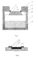
- the ring 3 with the seed wafer 1 was placed in the upper part of a growth chamber 6, by placing it on a protrusion 8 of the side wall of a chamber 6 and limiting it from above with a graphite isolation 4.
- a feedstock 5 also called SiC source material
- the seed wafer 1 was directed with its front surface (0001), having carbon polarity, towards the feedstock 5, while its back surface - was directed towards the colder part of the chamber 6. Both the front and back surface of the seed wafer 1, not covered with graphite elements, are subject to a sublimation process and the front surface is also subject to a process of deposition of a material diffusing from the feedstock 5.
- the empty space of the growth chamber 6 was filled with pure argon at a pressure of 20 mbar.
- the seed 1 was heated up to the temperature of 2200°C, measured with pyrometers on its back side, and adjusting temperature to consecutive steps of growth of the crystal 2.
- the lower part of the chamber 6 with the feedstock 5 was heated up to the temperature of 2400°C, also adjusting the temperature to consecutive steps of growth of the crystal 2.
- an 6H-SiC crystal 2 was obtained, having n-type electrical conductivity and having n-type carrier concentration of 3x10 17 cm -3 .
- the 6H-SiC crystal growth rate was 0.4mm/h.
- a layer 11 (approximately 2.5mm thick) of the seed 1 became carbonised during the process.
- the ring 3 together with the seed wafer 1 was placed in the upper part of the growth chamber 6, as in example 1.
- a feedstock 5, in a form of a pre-crystallized silicon carbide, was placed on the bottom of the growth chamber 6.
- the chamber 6 was filled with a mixture of argon and nitrogen in the ratio of 80:20, at a pressure of 60mbar, adjusted to crystallization temperature.
- the crystallization process was conducted at temperatures as in example 1.
- an 4H-SiC crystal 2 was obtained, having n-type electrical conductivity and having n-type carrier concentration of 1x10 19 cm -3 .
- the 4H-SiC crystal growth rate was 0.2 mm/h.
- a layer 11 (approximately 1.5mm thick) of the seed 1 became carbonised during the process.
- a feedstock 5 was placed in a form of a silicon carbide powder.
- a mixture of argon and nitrogen in the ratio of 90:10, at a pressure of 20mbar was used.
- the temperature measured on the crystal was 2200°C, and on the feedstock was 2400°C.
- an 4H-SiC crystal 2 was obtained, having n-type electrical conductivity and having n-type carrier concentration of 4x10 18 cm -3 .
- the 4H-SiC crystal growth rate was 0.4mm/h.
- a layer 11 (approximately 2.5mm thick) of the seed 1 became carbonised during the process.
- a feedstock 5 was placed in a form of a silicon carbide powder.
- pure nitrogen at a pressure of 50mbar was used as the growth atmosphere. The temperature measured on the crystal was 2100°C, and on the feedstock was 2200°C.
- an 4H-SiC crystal 2 was obtained, having n-type electrical conductivity and having n-type carrier concentration of 8x10 19 cm -3 .
- the 4H-SiC crystal growth rate was 0.05mm/h.
- a layer 11 (approximately 0.8mm thick) of the seed 1 became carbonised during the process.
- a feedstock 5 was placed in a form of a silicon carbide powder with boron as a dopant.
- pure argon at a pressure of 60mbar was used as the growth atmosphere. The temperature measured on the crystal was 2150°C, and on the feedstock was 2250°C.
- an 6H-SiC crystal 2 was obtained, having p-type electrical conductivity and having p-type carrier concentration of 2x10 14 cm -3 .
- the 6H-SiC crystal growth rate was 0.13mm/h.
- a layer 11 (approximately 1mm thick) of the seed 1 became carbonised during the process.
- a feedstock 5 was placed in a form of a silicon carbide powder with aluminium as a dopant.
- argon at a pressure of 80mbar was used as the growth atmosphere. The temperature measured on the crystal was 2100°C, and on the feedstock was 2200°C.
- an 6H-SiC crystal 2 was obtained, having p-type electrical conductivity and having p-type carrier concentration of 2x10 17 cm -3 .
- the 6H-SiC crystal growth rate was 0.02mm/h.
- a layer 11 (approximately 0.5mm thick) of the seed 1 became carbonised during the process.
- a feedstock 5 was placed in a form of a silicon carbide powder with vanadium as a dopant.
- a high purity argon at a pressure of 10mbar was used as the growth atmosphere. The temperature measured on the crystal was 2150°C, and on the feedstock was 2400°C.
- an 6H-SiC crystal 2 was obtained, having increased electrical resistivity of 1000 ⁇ /cm.
- the 6H-SiC crystal growth rate was 0.7mm/h.
- a layer 11 (approximately 3mm thick) of the seed 1 became carbonised during the process.
- an 6H-SiC crystal 2 was obtained, having n-type electrical conductivity and having n-type carrier concentration of 2x10 17 cm -3 .
- the 6H-SiC crystal growth rate was 0.4mm/h.
- a layer 11 (approximately 8mm thick) of the seed 1 became carbonised during the process.
- the 6H-SiC seed 1 wafer having only its silicon surface polished before the process.
- the seed wafer 1 was directed with its front surface (0001), having silicon polarity, towards the feedstock
- an 6H-SiC crystal 2 was obtained, having n-type electrical conductivity and having n-type carrier concentration of 2x10 17 cm -3 .
- the 6H-SiC crystal growth rate was 0.05mm/h.
- a layer 11 (approximately 3mm thick) of the seed 1 became carbonised during the process.
- an 4H-SiC crystal 2 was obtained, having n-type electrical conductivity and having n-type carrier concentration of 3x10 17 cm -3 .
- the 4H-SiC crystal growth rate was 0.4mm/h.
- a layer 11 (approximately 0.6mm thick) of the seed 1 became carbonised during the process.
- an 6H-SiC crystal 2 was obtained, having n-type electrical conductivity and having n-type carrier concentration of 2x10 17 cm -3 .
- the 6H-SiC crystal growth rate was 0.4mm/h. As shown in fig. 4 , only a thin layer 11 (approximately 0.2mm thick) of the seed 1 became carbonised during the process.
- an 6H-SiC crystal 2 was obtained, having n-type electrical conductivity and having n-type carrier concentration of 2x10 17 cm -3 .
- the 6H-SiC crystal growth rate was 0.4mm/h. As shown in fig. 5 , only a thin layer 11 (approximately 0.2mm thick) of the seed 1 became carbonised during the process.
- cerium-containing compounds in particular: Ce 2 O 3 , CeSi 2 , CeC 2 as well as elemental cerium.
- the cerium-containing compounds were added in the amount ranging from 0.1g to 10g, preferably about 0.3g (or: in the weight ratio with respect to the feedstock 5 ranging from 0.01 % to 1%, preferably about 0.03% - since usually the amount of feedstock 5 was 1000g). Similar favourable effect of preventing the undesired carbonisation of the seed 1 wand the obtained crystal 2 was observed in all such experiments.
Landscapes
- Chemical & Material Sciences (AREA)
- Engineering & Computer Science (AREA)
- Crystallography & Structural Chemistry (AREA)
- Materials Engineering (AREA)
- Metallurgy (AREA)
- Organic Chemistry (AREA)
- Inorganic Chemistry (AREA)
- Chemical Kinetics & Catalysis (AREA)
- General Chemical & Material Sciences (AREA)
- Crystals, And After-Treatments Of Crystals (AREA)
- Carbon And Carbon Compounds (AREA)
Abstract
Description
- The invention relates to a method for manufacturing crystals, in particular of silicon carbide, from gaseous phase, said crystals being applicable in high power electronics and optoelectronics as substrate materials for epitaxial structures.
- Known methods for obtaining silicon carbide crystals are based on application of monocrystalline seed in a form of thin wafer as the place for beginning the crystal growth.
- A method employing such a seed is known from a public publication Y.M. Tairov, V.F.Tsvetkow, J.Crystal Growth, 43 (1978) 209. This method consist in heating silicon carbide SiC feedstock material in a form of polycrystalline powder above the temperature of 2000°C. At this temperature sublimation of SiC, i.e. vaporisation and decomposition into Si, Si2, Si2C, SiC2 occurs, after which a process of crystallization proceeds on a monocrystalline seed, placed in the colder zone of the growth chamber. The process of crystallization lasts for 60-100 hours, a crystal obtained during that time has the length of 15-40mm.
- Suitably crystallographically oriented surface of a monocrystalline wafer is prepared in a process of grinding, polishing and chemical, electrochemical and/or thermal etching. The thus prepared wafer is placed on a holder, to which it may adhere by its weight, being sucked in by sub-pressure or adhesive forces or it may be glued with substances binding to the wafer and to the holder used.
- The common feature of known methods for mounting the seed to the holder is close matching of surfaces adhering to each other, described among others in the
US patent number 7316747 B2 . It consists in elimination of curvature of surfaces of the seed and the holder with a micrometer accuracy by polishing. To achieve this, a special geometry of polishing devices is used, which prevents the effect of rounding the surface during polishing. Another known method is filling the occurring gaps with a binder, such as carbon containing pastes. Binders used for this purpose must be resistant to high temperature, which in a technological process reaches 2400°C. Despite adhering, the binders must also tightly fill the gap occurring between the seed and the holder, on which the seed is placed. It is not fully possible, because all available binders decrease their volume during annealing. The occurring vacancies are the reason for bad crystalline quality of crystals, due to the phenomenon of migration of vacancies to the volume of the crystal. Microscopic smoothness of the holder, to which the seed is mounted, also influences the overall technological process. As the high temperature forces application of graphite or products based on graphite, such as graphite glass or metals having high melting temperature, a perfect smoothness of the surface of the holder is obtained by using graphite having a high density, so - having low porosity coefficient, and its mechanical treatment. In case a low density graphite, having a high porosity coefficient, is used, the obtained surface of the holder, even if prepared with utmost precision, is by its nature a rough surface. - In the technology of manufacturing of silicon carbide crystals, devices are used, whose interior - that is: the place of crystallization - is not accessible during the crystallization process. Everything is surrounded by a steel layer, covered with a water coating, which isolates heated elements from the outside surroundings. Controlling and temperature measurements are only possible in two points . The growing crystal is not being observed. Observation is only possible in the indirect way by X-raying the system, as described in the publication P.J. Wellman et al, J. Crystal Growth 216 (2000) 263. Therefore all phenomena related to incorrect mounting of the seed are only recognized after the crystallization process is finished. Because of that, the crystal growth process is often continued for many days without a chance for success. The obtained crystals are often not suitable for application in another step of technological process. Neither can they be used for manufacturing seeds, with which next crystals dedicated for seeds and restoring technological potential are produced.
- It is therefore the objective of the present invention to provide a method for manufacturing of single crystals, in particular of silicon carbide, wherein simplified way of mounting the seed is used, which enables a high efficiency of crystallization as well as shortening the time of preparing a crystallization process.
- The method according to the invention consists in that a monocrystalline seed in a form of a wafer, mounted in a ring made of high purity graphite in such way that only its edge abuts directly with the ring, is placed in the upper part of a growth chamber, filled with an inert gas or a gas ensuring doping of the crystal, with a feedstock placed on its bottom, after which the seed is heated up to the crystallization temperature under the condition of a high pressure of the gas filling the chamber, and a higher temperature in the lower part of the chamber is maintained, while preserving temperature difference between the feedstock and seed in the range from 50°C to 300°C and preferably parabolic character of the axial temperature profile.
- With such mounting of the seed, preferably a seed wafer is used having only one front surface polished.
- Preferably, the seed wafer is placed with its edge on a ring-shaped protrusion, being integrally formed with the ring, while the ring and the seed wafer is deposited on a protrusion of a side wall of the growth chamber. If needed, the edge of the seed is additionally sealed with a graphite paste or a silicon carbide paste.
- With such arrangement of the seed, the back surface of the seed (i.e. the surface of the seed directed away from the growth chamber) is essentially uncovered ("free"). As the result, no defects caused by e.g. incorrect gluing or coating of the back surface of the seed are introduced into the obtained crystal. Therefore, a higher crystalline quality is achieved.
- Usually the seed oriented in the plane (0001) is used, being crystallographically oriented along the direction parallel to crystallographic axis c, however it is also possible to use seeds of other crystallographic orientations.
- The seed wafer used preferably has a thickness from 0.2mm to 3mm.
- As the seed, preferably a wafer of silicon carbide is used, most preferably a wafer whose front surface has carbon or silicon polarity.
- As the feedstock, preferably silicon carbide is used, which - depending on the desired properties of the obtained crystal - is used undoped or enriched with dopants, such as boron, vanadium, aluminium, iron and/or redundant non-stoichiometric silicon.
- In order to obtain crystal doped with nitrogen, silicon carbide as a feedstock is placed in a growth chamber filled with nitrogen or a nitrogen-containing inert gas.
- As a gas filling the growth chamber, usually argon, nitrogen, hydrogen and/or helium is used.
- The seed is heated up preferably to the temperature from 1900°C to 2400°C, on its back surface.
- The process is conducted with a use of a temperature field and a field of partial pressures of vapours, out of which a crystal is formed, which fields are adjusted to crystal growth rates in the range from 0.01 mm/h to 2mm/h.
- Silicon carbide forms crystals, which are polar along their main crystallographic axis c. It means that two planes perpendicular to said c axis may be distinguished, called C-terminated plane (also: carbon plane, plane having carbon polarity) and Si-terminated side (also: silicon plane, plane having silicon polarity). The C-terminated plane is terminated with C atoms, while the S-terminated plane is terminated with Si atoms. These planes (surfaces of a crystal) have different physical and chemical properties. Crystal of the 4H-SiC polytype are obtained on the C-terminated surface of a monocrystalline seed, while crystals of the 6H-SiC polytype may be obtained on both C-terminated surface or Si-terminated surface of a monocrystalline seed. However, their growth on the Si-terminated surface is more stable.
- As explained above, the growth process according to the present invention is conducted with the back surface of the seed being uncovered. If the growth process is conducted on the Si-terminated surface of the seed - the other surface, being the C-terminated surface of the seed, is uncovered and vice versa. At process conditions, such an uncovered surface is subject to carbonization. The rate of carbonization depends on exact thermodynamical conditions of the growth process (in particular: on temperature and pressure). It is higher for the surface having carbon polarity and ranges from 0.01 mm/h to 0.15mm/h. For the surface having silicon polarity, the carbonization rate in approximately a few times lower. As the result of carbonization, a remarkable part of the obtained crystal may be lost.
- It was unexpectedly discovered, that an addition of cerium to the environment of the growth process remarkably (even by an order of magnitude) decreases the carbonization rate of the back surface of the seed, especially if that back surface has carbon polarity, comparing to a process in which cerium is not added. Most probably, cerium reacts with silicon atoms, producing a tight layer of graphite on the seed, which prevents sublimation of consecutive atomic layers of the seed (and the obtained crystal). Cerium may be introduced in any form - as elemental cerium or in a form of chemical compounds, such as CeO2, Ce2O3, CeSi2, CeC2 etc.
- Therefore, according to the invention, it is preferred that cerium, in the aforementioned form, is added to the environment of the growth process. It may be added directly to the growth chamber, in particular - may be mixed with the feedstock material or placed in a separate crucible inside the growth chamber. However, most preferably, it may be placed outside the growth chamber, but still in the vicinity of the monocrystalline seed. The latter arrangement outside the growth chamber does not influence the growth rate and the properties of the obtained crystal. It is particularly preferable to place cerium or a cerium-containing compound in a groove made in the graphite ring, used to seal the edges of the seed wafer.
- Preparation of a seed to the inventive crystallization process is limited to polishing only one front surface of the seed wafer, without the need to maintain flatness of the polished surface, which saves a lot of time comparing to known methods.
- The method according to the invention enables crystal growth rates many times higher than the rate of sublimation of the back surface of the seed and prevents rapid sublimation before the crystallization is started, while the shape and morphology of the crystallization front enables creation of a high quality crystal.
- The inventive method ensures a high reproducibility of the process as well as controlled doping, enabling manufacturing of crystals having a wide range of electrical properties. It also enables application of a non-conventional crystallization direction and using for crystallization different polytypes of silicon carbide, as well as other materials, such as for example AlN and ZnO.
- Preferred embodiments of the present invention are described below in a more detailed way with reference to the attached drawing, in which:
-
Fig. 1 presents an example of a system for manufacturing crystals from gaseous phase, by the method according to the present invention, as described in examples 1 to 9; -
fig. 2 presents a detailed view of the seed and the obtained crystal after the growth process, wherein the seed and part of the obtained crystal is carbonised, as described in examples 1 to 9; -
fig. 3 presents another example of a system for manufacturing crystals from gaseous phase, by the method according to the present invention, as described in example 12; -
fig. 4 presents a detailed view of the seed and the obtained crystal after the growth process, wherein only the surface of the seed is carbonised as described in examples 10 and 11 and -
fig. 5 presents a detailed view of the seed and the obtained crystal after the growth process, wherein only the surface of the seed is carbonised as described in example 12. - The examples described below illustrate the inventive method in specific, preferable embodiments.
- A
monocrystalline seed 1 of silicon carbide, having the orientation (0001), in a form of a 6H-SiC wafer, having a thickness of 1 mm and having only its carbon surface polished before the process, was mounted in aring 3 of a high purity graphite, such that the wafer was placed with its edge on a ring-shapedprotrusion 7, being integrally formed with thering 3, and sealed with agraphite ring 9. Thering 3 with theseed wafer 1 was placed in the upper part of agrowth chamber 6, by placing it on aprotrusion 8 of the side wall of achamber 6 and limiting it from above with agraphite isolation 4. On the bottom of thechamber 6, a feedstock 5 (also called SiC source material) in a form of a silicon carbide powder was deposited. - The
seed wafer 1 was directed with its front surface (0001), having carbon polarity, towards thefeedstock 5, while its back surface - was directed towards the colder part of thechamber 6. Both the front and back surface of theseed wafer 1, not covered with graphite elements, are subject to a sublimation process and the front surface is also subject to a process of deposition of a material diffusing from thefeedstock 5. - The empty space of the
growth chamber 6 was filled with pure argon at a pressure of 20 mbar. - The
seed 1 was heated up to the temperature of 2200°C, measured with pyrometers on its back side, and adjusting temperature to consecutive steps of growth of thecrystal 2. - The lower part of the
chamber 6 with thefeedstock 5 was heated up to the temperature of 2400°C, also adjusting the temperature to consecutive steps of growth of thecrystal 2. - After 75h of crystallization, an 6H-
SiC crystal 2 was obtained, having n-type electrical conductivity and having n-type carrier concentration of 3x1017cm-3. The 6H-SiC crystal growth rate was 0.4mm/h. As shown infig. 2 , a layer 11 (approximately 2.5mm thick) of theseed 1 became carbonised during the process. - A
monocrystalline seed 1 of silicon carbide, having the orientation (0001), in a form of a 4H-SiC wafer, having a thickness of 1mm, prepared as in example 1, was mounted in thering 3, as in example 1. Thering 3 together with theseed wafer 1 was placed in the upper part of thegrowth chamber 6, as in example 1. Afeedstock 5, in a form of a pre-crystallized silicon carbide, was placed on the bottom of thegrowth chamber 6. Thechamber 6 was filled with a mixture of argon and nitrogen in the ratio of 80:20, at a pressure of 60mbar, adjusted to crystallization temperature. The crystallization process was conducted at temperatures as in example 1. - After 75h of crystallization, an 4H-
SiC crystal 2 was obtained, having n-type electrical conductivity and having n-type carrier concentration of 1x1019cm-3. The 4H-SiC crystal growth rate was 0.2 mm/h. As shown infig. 2 , a layer 11 (approximately 1.5mm thick) of theseed 1 became carbonised during the process. - A
monocrystalline seed 1 of silicon carbide, having the orientation (0001), in a form of a 4H-SiC wafer, having a thickness of 1mm, prepared as in example 1, was mounted in thering 3 and placed in thechamber 6, as in example 1. On the bottom of thegrowth chamber 6, afeedstock 5 was placed in a form of a silicon carbide powder. As the growth atmosphere, a mixture of argon and nitrogen in the ratio of 90:10, at a pressure of 20mbar was used. The temperature measured on the crystal was 2200°C, and on the feedstock was 2400°C. - After 75h of crystallization, an 4H-
SiC crystal 2 was obtained, having n-type electrical conductivity and having n-type carrier concentration of 4x1018cm-3. The 4H-SiC crystal growth rate was 0.4mm/h. As shown infig. 2 , a layer 11 (approximately 2.5mm thick) of theseed 1 became carbonised during the process. - A
monocrystalline seed 1 of silicon carbide, having the orientation (0001), in a form of a 4H-SiC wafer, having the thickness of 1 mm, prepared as in example 1, was mounted in thering 3 and placed in thechamber 6, as in example 1. On the bottom of thegrowth chamber 6,afeedstock 5 was placed in a form of a silicon carbide powder. As the growth atmosphere, pure nitrogen at a pressure of 50mbar was used. The temperature measured on the crystal was 2100°C, and on the feedstock was 2200°C. - After 75h of crystallization, an 4H-
SiC crystal 2 was obtained, having n-type electrical conductivity and having n-type carrier concentration of 8x1019cm-3. The 4H-SiC crystal growth rate was 0.05mm/h. As shown infig. 2 , a layer 11 (approximately 0.8mm thick) of theseed 1 became carbonised during the process. - A
monocrystalline seed 1 of silicon carbide, having the orientation tilted off by 8° from the crystalline axis c, in a form of a 6H-SiC wafer, having a thickness of 0.5mm, prepared as in example 1, was mounted in thering 3 and placed in thechamber 6, as in example 1. On the bottom of thegrowth chamber 6, afeedstock 5 was placed in a form of a silicon carbide powder with boron as a dopant. As the growth atmosphere, pure argon at a pressure of 60mbar was used. The temperature measured on the crystal was 2150°C, and on the feedstock was 2250°C. - After 75h of crystallization, an 6H-
SiC crystal 2 was obtained, having p-type electrical conductivity and having p-type carrier concentration of 2x1014cm-3. The 6H-SiC crystal growth rate was 0.13mm/h. As shown infig. 2 , a layer 11 (approximately 1mm thick) of theseed 1 became carbonised during the process. - A
monocrystalline seed 1 of silicon carbide, having the orientation tilted off by 4° from the crystalline axis c, in a form of a 6H-SiC wafer, having a thickness of 1 mm, prepared as in example 1, was mounted in thering 3 and placed in thechamber 6, as in example 1. On the bottom of thegrowth chamber 6, afeedstock 5 was placed in a form of a silicon carbide powder with aluminium as a dopant. As the growth atmosphere, argon at a pressure of 80mbar was used. The temperature measured on the crystal was 2100°C, and on the feedstock was 2200°C. - After 75h of crystallization, an 6H-
SiC crystal 2 was obtained, having p-type electrical conductivity and having p-type carrier concentration of 2x1017cm-3. The 6H-SiC crystal growth rate was 0.02mm/h. As shown infig. 2 , a layer 11 (approximately 0.5mm thick) of theseed 1 became carbonised during the process. - A
monocrystalline seed 1 of silicon carbide, having the orientation tilted off by 2° from the crystalline axis c, in a form of a 6H-SiC wafer, having a thickness of 3mm, prepared as in example 1, was mounted in thering 3 and placed in thechamber 6, as in example 1. On the bottom of thegrowth chamber 6, afeedstock 5 was placed in a form of a silicon carbide powder with vanadium as a dopant. As the growth atmosphere, a high purity argon at a pressure of 10mbar was used. The temperature measured on the crystal was 2150°C, and on the feedstock was 2400°C. - After 75h of crystallization, an 6H-
SiC crystal 2 was obtained, having increased electrical resistivity of 1000Ω/cm. The 6H-SiC crystal growth rate was 0.7mm/h. As shown infig. 2 , a layer 11 (approximately 3mm thick) of theseed 1 became carbonised during the process. - Procedure as described in example 1 was repeated, however, the 6H-
SiC seed 1 wafer having only its silicon surface polished before the process. Theseed wafer 1 was directed with its front surface (0001), having silicon polarity, towards the feedstock. - After 75h of crystallization, an 6H-
SiC crystal 2 was obtained, having n-type electrical conductivity and having n-type carrier concentration of 2x1017cm-3. The 6H-SiC crystal growth rate was 0.4mm/h. As shown infig. 2 , a layer 11 (approximately 8mm thick) of theseed 1 became carbonised during the process. - Procedure as described in example 8 was repeated, however, as the growth atmosphere, a pressure of 60mbar was used. The temperature measured on the crystal was 2100°C, and on the feedstock was 2200°C.
- The 6H-
SiC seed 1 wafer having only its silicon surface polished before the process. Theseed wafer 1 was directed with its front surface (0001), having silicon polarity, towards the feedstock - After 75h of crystallization, an 6H-
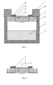
SiC crystal 2 was obtained, having n-type electrical conductivity and having n-type carrier concentration of 2x1017cm-3. The 6H-SiC crystal growth rate was 0.05mm/h. As shown infig. 2 , a layer 11 (approximately 3mm thick) of theseed 1 became carbonised during the process. - In all the aforementioned embodiments described in examples 1 to 9, the
seed 1 used, as well as apart 11 of the obtainedcrystal 2, was lost due to undesired carbonization, as can be seen infig. 2 , which presents a detailed view of theseed 1 and the obtainedcrystal 2 after such a growth process (carbonised part 11 is marked in dark colour, it may be even 8 mm thick). To prevent this, another process was conducted using a modified system, shown schematically infig. 3 . This system is very similar to that infig. 1 , however, thegraphite ring 9 comprises agroove 10, in which a cerium-containing compound may be placed or SiC source material was doped cerium compounds. - Procedure as described in example 1 was repeated, however, 0.5g of CeO2 was placed in the
feedstock 5. - After 75h of crystallization, an 4H-
SiC crystal 2 was obtained, having n-type electrical conductivity and having n-type carrier concentration of 3x1017cm-3. The 4H-SiC crystal growth rate was 0.4mm/h. As shown infig. 4 , a layer 11 (approximately 0.6mm thick) of theseed 1 became carbonised during the process. - Procedure as described in example 8 was repeated, however, the 6H-
SiC seed 1 wafer having only its silicon surface polished before the process. Theseed wafer 1 was directed with its front surface (0001), having silicon polarity, towards thefeedstock 5. Moreover, 1 g of CeSi2 was placed in thefeedstock 5. - After 75h of crystallization, an 6H-
SiC crystal 2 was obtained, having n-type electrical conductivity and having n-type carrier concentration of 2x1017cm-3. The 6H-SiC crystal growth rate was 0.4mm/h. As shown infig. 4 , only a thin layer 11 (approximately 0.2mm thick) of theseed 1 became carbonised during the process. - Procedure as described in example 8 was repeated, however, the 6H-
SiC seed 1 wafer having only its silicon surface polished before the process. Theseed wafer 1 was directed with its front surface (0001), having silicon polarity, towards thefeedstock 5. Moreover, 0.3g of CeO2 was placed in thegroove 10 in thegraphite ring 9 used to seal the edges of theseed wafer 1. - After 75h of crystallization, an 6H-
SiC crystal 2 was obtained, having n-type electrical conductivity and having n-type carrier concentration of 2x1017cm-3. The 6H-SiC crystal growth rate was 0.4mm/h. As shown infig. 5 , only a thin layer 11 (approximately 0.2mm thick) of theseed 1 became carbonised during the process. - Similar experiments as described in example 10 to 12 were performed, using other cerium-containing compounds, in particular: Ce2O3, CeSi2, CeC2 as well as elemental cerium. The cerium-containing compounds were added in the amount ranging from 0.1g to 10g, preferably about 0.3g (or: in the weight ratio with respect to the
feedstock 5 ranging from 0.01 % to 1%, preferably about 0.03% - since usually the amount offeedstock 5 was 1000g). Similar favourable effect of preventing the undesired carbonisation of theseed 1 wand the obtainedcrystal 2 was observed in all such experiments.
Claims (15)
- A method for manufacturing crystals, in particular of silicon carbide, from gaseous phase by heating a monocrystalline seed in a form of a wafer up to the temperature of crystallization in a graphite growth chamber filled with an inert gas or with a gas ensuring doping of the crystal, on the bottom of which chamber a feedstock is placed, characterized in that said monocrystalline seed (1) in a form of a wafer, mounted in a ring (3) of a high purity graphite such that only its edge abuts directly with the ring (3), the seed (1) is placed in the upper part of the growth chamber (6) filled with an inert gas or with a gas ensuring doping of the crystal, with the feedstock (5) deposited on its bottom, after which the seed (1) is heated up to the crystallization temperature at the condition of a high pressure of the gas filling the chamber (6) and a higher temperature in the lower part of the chamber (6) is maintained while preserving the temperature difference between the feedstock (5) and the seed (1) in the range from 50°C to 300°C and preferably parabolic character of the axial temperature profile.
- The method according to claim 1, characterized in that a seed (1) in a form of a wafer having only one front surface polished is used.
- The method according to claim 1 or 2, characterized in that a seed (1) in a form of a wafer deposited with its edge on a ring-shaped protrusion (7) being integrally formed with the ring (3) is used.
- The method according to any of claims 1 to 3, characterized in that the ring (3) together with the seed wafer (1) is deposited on a protrusion (8) of the side wall of the growth chamber (6).
- The method according to any of the preceding claims, characterized in that a seed (1) crystallographically oriented along the direction parallel to the crystalline axis c is used.
- The method according to any of the preceding claims, characterized in that a seed (1) in a form of a wafer having a thickness from 0.2mm to 3mm is used.
- The method according to any of the preceding claims, characterized in that as the seed (1), a wafer of silicon carbide is used, which wafer of silicone carbide preferably has the front surface of carbon polarity or of silicon polarity.
- The method according to any of the preceding claims, characterized in that silicon carbide, preferably doped with boron, vanadium, aluminium or a mixture thereof is used as the feedstock (5).
- The method according to claim 10, characterized in that silicon carbide having non-stoichiometric composition and comprising redundant silicon is used as the feedstock (5).
- The method according to claim 10, characterized in that silicon carbide used as the feedstock (5) is placed in the growth chamber (6), filled with nitrogen or with a nitrogen-containing inert gas.
- The method according to any of the preceding claims, characterized in that the seed (1) is heated up to the temperature from 1900°C to 2400°C on its back surface.
- The method according to any of the preceding claims, characterized in that the process is carried out using a temperature field and a field of partial pressures of vapours, out of which the crystal is created, adjusted to growth rates of the crystal (2) in the range from 0.01 mm/h to 2 mm/h.
- The method according to any of the preceding claims, characterized in that a cerium-containing compound is added to the environment of the growth process, preferably said cerium-containing compound being mixed with the feedstock (5), being placed in a separate crucible inside the growth chamber (6) or being placed in a groove (10), made in a ring (9) used to seal the edges of the seed wafer (1).
- The method according to claim 13, characterized in that said cerium-containing compound is selected from the group comprising CeO2, Ce2O3, CeSi2, CeC2, elemental cerium and mixtures thereof.
- The method according to claim 13 or 14, characterized in that said cerium-containing compound is added in the amount of 0.1g to 10g, preferably about 0.3g or in the weight ratio of 0.01% to 1%, preferably about 0.03%, with respect to the feedstock (5).
Applications Claiming Priority (1)
| Application Number | Priority Date | Filing Date | Title |
|---|---|---|---|
| PL390896A PL234396B1 (en) | 2010-04-01 | 2010-04-01 | Process for the preparation of crystals, especially silicon carbide from the gas phase |
Publications (2)
| Publication Number | Publication Date |
|---|---|
| EP2371997A1 true EP2371997A1 (en) | 2011-10-05 |
| EP2371997B1 EP2371997B1 (en) | 2017-01-11 |
Family
ID=44084055
Family Applications (1)
| Application Number | Title | Priority Date | Filing Date |
|---|---|---|---|
| EP11159952.8A Active EP2371997B1 (en) | 2010-04-01 | 2011-03-28 | Method for manufacturing crystals of silicon carbide from gaseous phase |
Country Status (2)
| Country | Link |
|---|---|
| EP (1) | EP2371997B1 (en) |
| PL (1) | PL234396B1 (en) |
Cited By (12)
| Publication number | Priority date | Publication date | Assignee | Title |
|---|---|---|---|---|
| WO2014123636A1 (en) * | 2013-02-05 | 2014-08-14 | Dow Corning Corporation | Sic crystal with low dislocation density |
| WO2014123635A1 (en) * | 2013-02-05 | 2014-08-14 | Dow Corning Corporation | Sic crystal and wafer cut from crystal with low dislocation density |
| US8860040B2 (en) | 2012-09-11 | 2014-10-14 | Dow Corning Corporation | High voltage power semiconductor devices on SiC |
| US8940614B2 (en) | 2013-03-15 | 2015-01-27 | Dow Corning Corporation | SiC substrate with SiC epitaxial film |
| US9017804B2 (en) | 2013-02-05 | 2015-04-28 | Dow Corning Corporation | Method to reduce dislocations in SiC crystal growth |
| US9018639B2 (en) | 2012-10-26 | 2015-04-28 | Dow Corning Corporation | Flat SiC semiconductor substrate |
| US9279192B2 (en) | 2014-07-29 | 2016-03-08 | Dow Corning Corporation | Method for manufacturing SiC wafer fit for integration with power device manufacturing technology |
| EP3072995A1 (en) * | 2015-03-25 | 2016-09-28 | Instytut Technologii Materialów Elektronicznych | Method for producing silicon carbide crystals from vapour phase |
| RU2633909C1 (en) * | 2016-12-23 | 2017-10-19 | Федеральное государственное автономное образовательное учреждение высшего образования "Санкт-Петербургский государственный электротехнический университет "ЛЭТИ" им. В.И. Ульянова (Ленина)" (СПбГЭТУ "ЛЭТИ") | METHOD OF PRODUCING MONOCRYSTALLINE SiC |
| CN111593407A (en) * | 2020-05-25 | 2020-08-28 | 北京北方华创微电子装备有限公司 | Silicon carbide growth method |
| RU2768938C1 (en) * | 2021-10-14 | 2022-03-25 | Санкт-Петербургский государственный электротехнический университет ЛЭТИ им. В.И. Ульянова (Ленина) | Method for producing single-crystal sic polytype 4h |
| CN116553554A (en) * | 2023-04-21 | 2023-08-08 | 昆明云锗高新技术有限公司 | Silicon carbide powder synthesis method |
Citations (7)
| Publication number | Priority date | Publication date | Assignee | Title |
|---|---|---|---|---|
| JPH0230699A (en) * | 1988-04-13 | 1990-02-01 | Nippon Steel Corp | Growing method of silicon carbide single crystal and device therefor |
| WO2001063020A1 (en) * | 2000-02-15 | 2001-08-30 | The Fox Group, Inc. | Method and apparatus for growing low defect density silicon carbide and resulting material |
| US20020083892A1 (en) * | 2000-12-28 | 2002-07-04 | Hiroyuki Kondo | Method and apparatus for producing single crystal, substrate for growing single crystal and method for heating single crystal |
| US20020088391A1 (en) * | 1999-07-07 | 2002-07-11 | Harald Kuhn | Seed crystal holder with lateral mount for an SiC seed crystal |
| US20060107890A1 (en) * | 2002-06-24 | 2006-05-25 | Hobgood Hudson M | One hundred millimeter single crystal silicon carbide wafer |
| US7316747B2 (en) | 2002-06-24 | 2008-01-08 | Cree, Inc. | Seeded single crystal silicon carbide growth and resulting crystals |
| WO2009026269A1 (en) * | 2007-08-20 | 2009-02-26 | Ii-Vi Incorporated | Stabilizing 4h polytype during sublimation growth of sic single crystals |
-
2010
- 2010-04-01 PL PL390896A patent/PL234396B1/en unknown
-
2011
- 2011-03-28 EP EP11159952.8A patent/EP2371997B1/en active Active
Patent Citations (7)
| Publication number | Priority date | Publication date | Assignee | Title |
|---|---|---|---|---|
| JPH0230699A (en) * | 1988-04-13 | 1990-02-01 | Nippon Steel Corp | Growing method of silicon carbide single crystal and device therefor |
| US20020088391A1 (en) * | 1999-07-07 | 2002-07-11 | Harald Kuhn | Seed crystal holder with lateral mount for an SiC seed crystal |
| WO2001063020A1 (en) * | 2000-02-15 | 2001-08-30 | The Fox Group, Inc. | Method and apparatus for growing low defect density silicon carbide and resulting material |
| US20020083892A1 (en) * | 2000-12-28 | 2002-07-04 | Hiroyuki Kondo | Method and apparatus for producing single crystal, substrate for growing single crystal and method for heating single crystal |
| US20060107890A1 (en) * | 2002-06-24 | 2006-05-25 | Hobgood Hudson M | One hundred millimeter single crystal silicon carbide wafer |
| US7316747B2 (en) | 2002-06-24 | 2008-01-08 | Cree, Inc. | Seeded single crystal silicon carbide growth and resulting crystals |
| WO2009026269A1 (en) * | 2007-08-20 | 2009-02-26 | Ii-Vi Incorporated | Stabilizing 4h polytype during sublimation growth of sic single crystals |
Non-Patent Citations (4)
| Title |
|---|
| "Silicon Carbide and Related Materials 2009", 1 April 2010, TRANS TECH PUBLICATION LTD, Switzerland-UK-USA, ISBN: 978-0-87-849279-4, article "Silicon Carbide and Related Materials 2009", pages: x - xix, XP055004610 * |
| P.J. WELLMAN ET AL., J. CRYSTAL GROWTH, vol. 216, 2000, pages 263 |
| TYMICKI E ET AL: "Growth of 4H-SiC crystals on the 8[deg.] off-axis 6H-SiC seed by PVT method", MATERIALS SCIENCE FORUM, AEDERMANNSFDORF, CH, vol. 645-648, 1 April 2010 (2010-04-01), pages 17 - 20, XP008140239, ISSN: 0255-5476, [retrieved on 20100101], DOI: 10.4028/WWW.SCIENTIFIC.NET/MSF.645-648.17 * |
| Y.M. TAIROV, V.F.TSVETKOW, J.CRYSTAL GROWTH, vol. 43, 1978, pages 209 |
Cited By (23)
| Publication number | Priority date | Publication date | Assignee | Title |
|---|---|---|---|---|
| US8860040B2 (en) | 2012-09-11 | 2014-10-14 | Dow Corning Corporation | High voltage power semiconductor devices on SiC |
| US9337277B2 (en) | 2012-09-11 | 2016-05-10 | Dow Corning Corporation | High voltage power semiconductor device on SiC |
| US9018639B2 (en) | 2012-10-26 | 2015-04-28 | Dow Corning Corporation | Flat SiC semiconductor substrate |
| US9165779B2 (en) | 2012-10-26 | 2015-10-20 | Dow Corning Corporation | Flat SiC semiconductor substrate |
| US9738991B2 (en) | 2013-02-05 | 2017-08-22 | Dow Corning Corporation | Method for growing a SiC crystal by vapor deposition onto a seed crystal provided on a supporting shelf which permits thermal expansion |
| WO2014123636A1 (en) * | 2013-02-05 | 2014-08-14 | Dow Corning Corporation | Sic crystal with low dislocation density |
| US9017804B2 (en) | 2013-02-05 | 2015-04-28 | Dow Corning Corporation | Method to reduce dislocations in SiC crystal growth |
| CN105008596A (en) * | 2013-02-05 | 2015-10-28 | 道康宁公司 | Sic crystal with low dislocation density |
| CN105051268A (en) * | 2013-02-05 | 2015-11-11 | 道康宁公司 | SiC crystal and wafer cut from crystal with low dislocation density |
| WO2014123635A1 (en) * | 2013-02-05 | 2014-08-14 | Dow Corning Corporation | Sic crystal and wafer cut from crystal with low dislocation density |
| CN105008596B (en) * | 2013-02-05 | 2020-01-03 | 美国陶氏有机硅公司 | SIC crystals with low dislocation density |
| US9797064B2 (en) | 2013-02-05 | 2017-10-24 | Dow Corning Corporation | Method for growing a SiC crystal by vapor deposition onto a seed crystal provided on a support shelf which permits thermal expansion |
| US10435810B2 (en) * | 2013-02-05 | 2019-10-08 | Dow Silicones Corporation | Graphite crucible for sublimation growth of SiC crystal |
| US8940614B2 (en) | 2013-03-15 | 2015-01-27 | Dow Corning Corporation | SiC substrate with SiC epitaxial film |
| US9279192B2 (en) | 2014-07-29 | 2016-03-08 | Dow Corning Corporation | Method for manufacturing SiC wafer fit for integration with power device manufacturing technology |
| US10002760B2 (en) | 2014-07-29 | 2018-06-19 | Dow Silicones Corporation | Method for manufacturing SiC wafer fit for integration with power device manufacturing technology |
| EP3072995A1 (en) * | 2015-03-25 | 2016-09-28 | Instytut Technologii Materialów Elektronicznych | Method for producing silicon carbide crystals from vapour phase |
| RU2633909C1 (en) * | 2016-12-23 | 2017-10-19 | Федеральное государственное автономное образовательное учреждение высшего образования "Санкт-Петербургский государственный электротехнический университет "ЛЭТИ" им. В.И. Ульянова (Ленина)" (СПбГЭТУ "ЛЭТИ") | METHOD OF PRODUCING MONOCRYSTALLINE SiC |
| CN111593407A (en) * | 2020-05-25 | 2020-08-28 | 北京北方华创微电子装备有限公司 | Silicon carbide growth method |
| CN111593407B (en) * | 2020-05-25 | 2021-12-17 | 北京北方华创微电子装备有限公司 | Silicon carbide growth method |
| RU2768938C1 (en) * | 2021-10-14 | 2022-03-25 | Санкт-Петербургский государственный электротехнический университет ЛЭТИ им. В.И. Ульянова (Ленина) | Method for producing single-crystal sic polytype 4h |
| CN116553554A (en) * | 2023-04-21 | 2023-08-08 | 昆明云锗高新技术有限公司 | Silicon carbide powder synthesis method |
| CN116553554B (en) * | 2023-04-21 | 2024-05-14 | 昆明云锗高新技术有限公司 | Silicon carbide powder synthesis method |
Also Published As
| Publication number | Publication date |
|---|---|
| PL234396B1 (en) | 2020-02-28 |
| EP2371997B1 (en) | 2017-01-11 |
| PL390896A1 (en) | 2011-10-10 |
Similar Documents
| Publication | Publication Date | Title |
|---|---|---|
| EP2371997B1 (en) | Method for manufacturing crystals of silicon carbide from gaseous phase | |
| KR100951019B1 (en) | Monocrystalline silicon carbide ingot and monocrystalline silicon carbide wafer | |
| TWI770769B (en) | Vapor deposition apparatus and techniques using high purity polymer derived silicon carbide | |
| EP2851456A1 (en) | Large Diameter, High Quality SiC Single Crystals, Method and Apparatus | |
| KR102284879B1 (en) | SiC WAFER, PREPARATION METHOD OF SiC WAFER | |
| KR100773624B1 (en) | Seed crystal of silicon carbide single crystal and method for producing ingot using same | |
| JP4733485B2 (en) | Method for producing seed crystal for silicon carbide single crystal growth, seed crystal for silicon carbide single crystal growth, method for producing silicon carbide single crystal, and silicon carbide single crystal | |
| US20090053125A1 (en) | Stabilizing 4H Polytype During Sublimation Growth Of SiC Single Crystals | |
| EP3382068B1 (en) | Silicon carbide substrate and method of growing sic single crystal boules | |
| KR101793394B1 (en) | N-TYPE SiC SINGLE CRYSTAL AND METHOD FOR PRODUCING SAME | |
| JP2007153719A (en) | Method for producing silicon carbide single crystal | |
| KR101788905B1 (en) | Feed material for epitaxial growth of monocrystalline silicon carbide, and method for epitaxial growth of monocrystalline silicon carbide | |
| KR101788906B1 (en) | Seed material for liquid phase epitaxial growth of monocrystalline silicon carbide, and method for liquid phase epitaxial growth of monocrystalline silicon carbide | |
| CN107190322B (en) | A kind of growing method of the adjustable silicon carbide polycrystalline ceramics of large scale resistivity | |
| Semmelroth et al. | Growth of SiC polytypes by the physical vapour transport technique | |
| KR101740094B1 (en) | Unit for liquid phase epitaxial growth of monocrystalline silicon carbide, and method for liquid phase epitaxial growth of monocrystalline silicon carbide | |
| KR102187449B1 (en) | PREPERATION METHOD FOR SiC INGOT, THE SiC INGOT AND A SYSTEM THEREOF | |
| EP3072995B1 (en) | Method for producing silicon carbide crystals from vapour phase | |
| KR101767295B1 (en) | Seed material for liquid phase epitaxial growth of monocrystalline silicon carbide, and method for liquid phase epitaxial growth of monocrystalline silicon | |
| EP4144895A1 (en) | Silicon carbide ingot manufacturing method, silicon carbide ingots, and growth system therefor | |
| JP5724121B2 (en) | Feed material for epitaxial growth of single crystal silicon carbide and epitaxial growth method of single crystal silicon carbide | |
| JP5707612B2 (en) | Single crystal silicon carbide liquid phase epitaxial growth unit and single crystal silicon carbide liquid phase epitaxial growth method | |
| Lee et al. | Vanadium-doped semi-insulating SiC single crystal growth by using porous graphite | |
| JP2012136364A (en) | Seed material for liquid phase epitaxial growth of single crystal silicon carbide and method for liquid phase epitaxial growth of single crystal silicon carbide |
Legal Events
| Date | Code | Title | Description |
|---|---|---|---|
| PUAI | Public reference made under article 153(3) epc to a published international application that has entered the european phase |
Free format text: ORIGINAL CODE: 0009012 |
|
| AK | Designated contracting states |
Kind code of ref document: A1 Designated state(s): AL AT BE BG CH CY CZ DE DK EE ES FI FR GB GR HR HU IE IS IT LI LT LU LV MC MK MT NL NO PL PT RO RS SE SI SK SM TR |
|
| AX | Request for extension of the european patent |
Extension state: BA ME |
|
| 17P | Request for examination filed |
Effective date: 20120315 |
|
| 17Q | First examination report despatched |
Effective date: 20160104 |
|
| GRAP | Despatch of communication of intention to grant a patent |
Free format text: ORIGINAL CODE: EPIDOSNIGR1 |
|
| INTG | Intention to grant announced |
Effective date: 20160802 |
|
| GRAS | Grant fee paid |
Free format text: ORIGINAL CODE: EPIDOSNIGR3 |
|
| GRAA | (expected) grant |
Free format text: ORIGINAL CODE: 0009210 |
|
| AK | Designated contracting states |
Kind code of ref document: B1 Designated state(s): AL AT BE BG CH CY CZ DE DK EE ES FI FR GB GR HR HU IE IS IT LI LT LU LV MC MK MT NL NO PL PT RO RS SE SI SK SM TR |
|
| REG | Reference to a national code |
Ref country code: GB Ref legal event code: FG4D |
|
| REG | Reference to a national code |
Ref country code: CH Ref legal event code: EP |
|
| REG | Reference to a national code |
Ref country code: AT Ref legal event code: REF Ref document number: 861369 Country of ref document: AT Kind code of ref document: T Effective date: 20170115 |
|
| REG | Reference to a national code |
Ref country code: IE Ref legal event code: FG4D |
|
| REG | Reference to a national code |
Ref country code: FR Ref legal event code: PLFP Year of fee payment: 7 |
|
| REG | Reference to a national code |
Ref country code: DE Ref legal event code: R096 Ref document number: 602011034212 Country of ref document: DE |
|
| REG | Reference to a national code |
Ref country code: LT Ref legal event code: MG4D |
|
| REG | Reference to a national code |
Ref country code: NL Ref legal event code: MP Effective date: 20170111 |
|
| REG | Reference to a national code |
Ref country code: AT Ref legal event code: MK05 Ref document number: 861369 Country of ref document: AT Kind code of ref document: T Effective date: 20170111 |
|
| PG25 | Lapsed in a contracting state [announced via postgrant information from national office to epo] |
Ref country code: NL Free format text: LAPSE BECAUSE OF FAILURE TO SUBMIT A TRANSLATION OF THE DESCRIPTION OR TO PAY THE FEE WITHIN THE PRESCRIBED TIME-LIMIT Effective date: 20170111 |
|
| PG25 | Lapsed in a contracting state [announced via postgrant information from national office to epo] |
Ref country code: IS Free format text: LAPSE BECAUSE OF FAILURE TO SUBMIT A TRANSLATION OF THE DESCRIPTION OR TO PAY THE FEE WITHIN THE PRESCRIBED TIME-LIMIT Effective date: 20170511 Ref country code: LT Free format text: LAPSE BECAUSE OF FAILURE TO SUBMIT A TRANSLATION OF THE DESCRIPTION OR TO PAY THE FEE WITHIN THE PRESCRIBED TIME-LIMIT Effective date: 20170111 Ref country code: FI Free format text: LAPSE BECAUSE OF FAILURE TO SUBMIT A TRANSLATION OF THE DESCRIPTION OR TO PAY THE FEE WITHIN THE PRESCRIBED TIME-LIMIT Effective date: 20170111 Ref country code: NO Free format text: LAPSE BECAUSE OF FAILURE TO SUBMIT A TRANSLATION OF THE DESCRIPTION OR TO PAY THE FEE WITHIN THE PRESCRIBED TIME-LIMIT Effective date: 20170411 Ref country code: GR Free format text: LAPSE BECAUSE OF FAILURE TO SUBMIT A TRANSLATION OF THE DESCRIPTION OR TO PAY THE FEE WITHIN THE PRESCRIBED TIME-LIMIT Effective date: 20170412 Ref country code: HR Free format text: LAPSE BECAUSE OF FAILURE TO SUBMIT A TRANSLATION OF THE DESCRIPTION OR TO PAY THE FEE WITHIN THE PRESCRIBED TIME-LIMIT Effective date: 20170111 |
|
| PG25 | Lapsed in a contracting state [announced via postgrant information from national office to epo] |
Ref country code: ES Free format text: LAPSE BECAUSE OF FAILURE TO SUBMIT A TRANSLATION OF THE DESCRIPTION OR TO PAY THE FEE WITHIN THE PRESCRIBED TIME-LIMIT Effective date: 20170111 Ref country code: AT Free format text: LAPSE BECAUSE OF FAILURE TO SUBMIT A TRANSLATION OF THE DESCRIPTION OR TO PAY THE FEE WITHIN THE PRESCRIBED TIME-LIMIT Effective date: 20170111 Ref country code: RS Free format text: LAPSE BECAUSE OF FAILURE TO SUBMIT A TRANSLATION OF THE DESCRIPTION OR TO PAY THE FEE WITHIN THE PRESCRIBED TIME-LIMIT Effective date: 20170111 Ref country code: SE Free format text: LAPSE BECAUSE OF FAILURE TO SUBMIT A TRANSLATION OF THE DESCRIPTION OR TO PAY THE FEE WITHIN THE PRESCRIBED TIME-LIMIT Effective date: 20170111 Ref country code: LV Free format text: LAPSE BECAUSE OF FAILURE TO SUBMIT A TRANSLATION OF THE DESCRIPTION OR TO PAY THE FEE WITHIN THE PRESCRIBED TIME-LIMIT Effective date: 20170111 Ref country code: PT Free format text: LAPSE BECAUSE OF FAILURE TO SUBMIT A TRANSLATION OF THE DESCRIPTION OR TO PAY THE FEE WITHIN THE PRESCRIBED TIME-LIMIT Effective date: 20170511 Ref country code: BG Free format text: LAPSE BECAUSE OF FAILURE TO SUBMIT A TRANSLATION OF THE DESCRIPTION OR TO PAY THE FEE WITHIN THE PRESCRIBED TIME-LIMIT Effective date: 20170411 Ref country code: PL Free format text: LAPSE BECAUSE OF FAILURE TO SUBMIT A TRANSLATION OF THE DESCRIPTION OR TO PAY THE FEE WITHIN THE PRESCRIBED TIME-LIMIT Effective date: 20170111 |
|
| REG | Reference to a national code |
Ref country code: DE Ref legal event code: R097 Ref document number: 602011034212 Country of ref document: DE |
|
| PG25 | Lapsed in a contracting state [announced via postgrant information from national office to epo] |
Ref country code: IT Free format text: LAPSE BECAUSE OF FAILURE TO SUBMIT A TRANSLATION OF THE DESCRIPTION OR TO PAY THE FEE WITHIN THE PRESCRIBED TIME-LIMIT Effective date: 20170111 Ref country code: EE Free format text: LAPSE BECAUSE OF FAILURE TO SUBMIT A TRANSLATION OF THE DESCRIPTION OR TO PAY THE FEE WITHIN THE PRESCRIBED TIME-LIMIT Effective date: 20170111 Ref country code: CZ Free format text: LAPSE BECAUSE OF FAILURE TO SUBMIT A TRANSLATION OF THE DESCRIPTION OR TO PAY THE FEE WITHIN THE PRESCRIBED TIME-LIMIT Effective date: 20170111 Ref country code: RO Free format text: LAPSE BECAUSE OF FAILURE TO SUBMIT A TRANSLATION OF THE DESCRIPTION OR TO PAY THE FEE WITHIN THE PRESCRIBED TIME-LIMIT Effective date: 20170111 Ref country code: SK Free format text: LAPSE BECAUSE OF FAILURE TO SUBMIT A TRANSLATION OF THE DESCRIPTION OR TO PAY THE FEE WITHIN THE PRESCRIBED TIME-LIMIT Effective date: 20170111 |
|
| REG | Reference to a national code |
Ref country code: CH Ref legal event code: PL |
|
| PLBE | No opposition filed within time limit |
Free format text: ORIGINAL CODE: 0009261 |
|
| STAA | Information on the status of an ep patent application or granted ep patent |
Free format text: STATUS: NO OPPOSITION FILED WITHIN TIME LIMIT |
|
| PG25 | Lapsed in a contracting state [announced via postgrant information from national office to epo] |
Ref country code: MC Free format text: LAPSE BECAUSE OF FAILURE TO SUBMIT A TRANSLATION OF THE DESCRIPTION OR TO PAY THE FEE WITHIN THE PRESCRIBED TIME-LIMIT Effective date: 20170111 Ref country code: DK Free format text: LAPSE BECAUSE OF FAILURE TO SUBMIT A TRANSLATION OF THE DESCRIPTION OR TO PAY THE FEE WITHIN THE PRESCRIBED TIME-LIMIT Effective date: 20170111 Ref country code: SM Free format text: LAPSE BECAUSE OF FAILURE TO SUBMIT A TRANSLATION OF THE DESCRIPTION OR TO PAY THE FEE WITHIN THE PRESCRIBED TIME-LIMIT Effective date: 20170111 |
|
| 26N | No opposition filed |
Effective date: 20171012 |
|
| REG | Reference to a national code |
Ref country code: IE Ref legal event code: MM4A |
|
| PG25 | Lapsed in a contracting state [announced via postgrant information from national office to epo] |
Ref country code: LU Free format text: LAPSE BECAUSE OF NON-PAYMENT OF DUE FEES Effective date: 20170328 |
|
| PG25 | Lapsed in a contracting state [announced via postgrant information from national office to epo] |
Ref country code: CH Free format text: LAPSE BECAUSE OF NON-PAYMENT OF DUE FEES Effective date: 20170331 Ref country code: SI Free format text: LAPSE BECAUSE OF FAILURE TO SUBMIT A TRANSLATION OF THE DESCRIPTION OR TO PAY THE FEE WITHIN THE PRESCRIBED TIME-LIMIT Effective date: 20170111 Ref country code: IE Free format text: LAPSE BECAUSE OF NON-PAYMENT OF DUE FEES Effective date: 20170328 Ref country code: LI Free format text: LAPSE BECAUSE OF NON-PAYMENT OF DUE FEES Effective date: 20170331 |
|
| REG | Reference to a national code |
Ref country code: FR Ref legal event code: PLFP Year of fee payment: 8 |
|
| REG | Reference to a national code |
Ref country code: BE Ref legal event code: MM Effective date: 20170331 |
|
| PGFP | Annual fee paid to national office [announced via postgrant information from national office to epo] |
Ref country code: GB Payment date: 20180306 Year of fee payment: 8 |
|
| PG25 | Lapsed in a contracting state [announced via postgrant information from national office to epo] |
Ref country code: BE Free format text: LAPSE BECAUSE OF NON-PAYMENT OF DUE FEES Effective date: 20170331 |
|
| PGFP | Annual fee paid to national office [announced via postgrant information from national office to epo] |
Ref country code: FR Payment date: 20180305 Year of fee payment: 8 |
|
| PG25 | Lapsed in a contracting state [announced via postgrant information from national office to epo] |
Ref country code: MT Free format text: LAPSE BECAUSE OF NON-PAYMENT OF DUE FEES Effective date: 20170328 |
|
| PG25 | Lapsed in a contracting state [announced via postgrant information from national office to epo] |
Ref country code: HU Free format text: LAPSE BECAUSE OF FAILURE TO SUBMIT A TRANSLATION OF THE DESCRIPTION OR TO PAY THE FEE WITHIN THE PRESCRIBED TIME-LIMIT; INVALID AB INITIO Effective date: 20110328 |
|
| PG25 | Lapsed in a contracting state [announced via postgrant information from national office to epo] |
Ref country code: CY Free format text: LAPSE BECAUSE OF NON-PAYMENT OF DUE FEES Effective date: 20170111 |
|
| GBPC | Gb: european patent ceased through non-payment of renewal fee |
Effective date: 20190328 |
|
| PG25 | Lapsed in a contracting state [announced via postgrant information from national office to epo] |
Ref country code: MK Free format text: LAPSE BECAUSE OF FAILURE TO SUBMIT A TRANSLATION OF THE DESCRIPTION OR TO PAY THE FEE WITHIN THE PRESCRIBED TIME-LIMIT Effective date: 20170111 |
|
| PG25 | Lapsed in a contracting state [announced via postgrant information from national office to epo] |
Ref country code: GB Free format text: LAPSE BECAUSE OF NON-PAYMENT OF DUE FEES Effective date: 20190328 |
|
| PG25 | Lapsed in a contracting state [announced via postgrant information from national office to epo] |
Ref country code: FR Free format text: LAPSE BECAUSE OF NON-PAYMENT OF DUE FEES Effective date: 20190331 |
|
| PG25 | Lapsed in a contracting state [announced via postgrant information from national office to epo] |
Ref country code: TR Free format text: LAPSE BECAUSE OF FAILURE TO SUBMIT A TRANSLATION OF THE DESCRIPTION OR TO PAY THE FEE WITHIN THE PRESCRIBED TIME-LIMIT Effective date: 20170111 |
|
| PG25 | Lapsed in a contracting state [announced via postgrant information from national office to epo] |
Ref country code: AL Free format text: LAPSE BECAUSE OF FAILURE TO SUBMIT A TRANSLATION OF THE DESCRIPTION OR TO PAY THE FEE WITHIN THE PRESCRIBED TIME-LIMIT Effective date: 20170111 |
|
| PGFP | Annual fee paid to national office [announced via postgrant information from national office to epo] |
Ref country code: DE Payment date: 20230327 Year of fee payment: 13 |