EP2360493A1 - Detector arrangement for a tomographic imaging apparatus, particularly for a positron emission tomograph - Google Patents
Detector arrangement for a tomographic imaging apparatus, particularly for a positron emission tomograph Download PDFInfo
- Publication number
- EP2360493A1 EP2360493A1 EP10001529A EP10001529A EP2360493A1 EP 2360493 A1 EP2360493 A1 EP 2360493A1 EP 10001529 A EP10001529 A EP 10001529A EP 10001529 A EP10001529 A EP 10001529A EP 2360493 A1 EP2360493 A1 EP 2360493A1
- Authority
- EP
- European Patent Office
- Prior art keywords
- detector
- scintillators
- energy
- detector arrangement
- detections
- Prior art date
- Legal status (The legal status is an assumption and is not a legal conclusion. Google has not performed a legal analysis and makes no representation as to the accuracy of the status listed.)
- Withdrawn
Links
- 238000003384 imaging method Methods 0.000 title claims abstract description 16
- 238000001514 detection method Methods 0.000 claims abstract description 96
- 230000003287 optical effect Effects 0.000 claims description 28
- 238000011017 operating method Methods 0.000 claims description 15
- 238000009413 insulation Methods 0.000 claims description 14
- 238000010191 image analysis Methods 0.000 claims description 10
- 230000005855 radiation Effects 0.000 claims description 7
- 239000004744 fabric Substances 0.000 claims description 6
- 230000004044 response Effects 0.000 claims description 6
- XUIMIQQOPSSXEZ-UHFFFAOYSA-N Silicon Chemical compound [Si] XUIMIQQOPSSXEZ-UHFFFAOYSA-N 0.000 claims description 5
- 229910052710 silicon Inorganic materials 0.000 claims description 5
- 239000010703 silicon Substances 0.000 claims description 5
- 238000004364 calculation method Methods 0.000 claims description 4
- 238000003325 tomography Methods 0.000 claims description 3
- 239000004775 Tyvek Substances 0.000 claims description 2
- 229920000690 Tyvek Polymers 0.000 claims description 2
- 238000005253 cladding Methods 0.000 claims description 2
- 238000012937 correction Methods 0.000 claims description 2
- 238000005259 measurement Methods 0.000 claims description 2
- 239000002159 nanocrystal Substances 0.000 claims description 2
- 239000003973 paint Substances 0.000 claims description 2
- KEAYESYHFKHZAL-UHFFFAOYSA-N Sodium Chemical compound [Na] KEAYESYHFKHZAL-UHFFFAOYSA-N 0.000 claims 1
- ATJFFYVFTNAWJD-UHFFFAOYSA-N Tin Chemical compound [Sn] ATJFFYVFTNAWJD-UHFFFAOYSA-N 0.000 claims 1
- 229910052788 barium Inorganic materials 0.000 claims 1
- DSAJWYNOEDNPEQ-UHFFFAOYSA-N barium atom Chemical compound [Ba] DSAJWYNOEDNPEQ-UHFFFAOYSA-N 0.000 claims 1
- 229910052792 caesium Inorganic materials 0.000 claims 1
- 229910017052 cobalt Inorganic materials 0.000 claims 1
- 239000010941 cobalt Substances 0.000 claims 1
- GUTLYIVDDKVIGB-UHFFFAOYSA-N cobalt atom Chemical compound [Co] GUTLYIVDDKVIGB-UHFFFAOYSA-N 0.000 claims 1
- 238000004519 manufacturing process Methods 0.000 claims 1
- 229910052708 sodium Inorganic materials 0.000 claims 1
- 239000011734 sodium Substances 0.000 claims 1
- 230000000087 stabilizing effect Effects 0.000 claims 1
- 230000003746 surface roughness Effects 0.000 claims 1
- 238000004381 surface treatment Methods 0.000 claims 1
- 239000013078 crystal Substances 0.000 description 26
- 239000010410 layer Substances 0.000 description 15
- XQPRBTXUXXVTKB-UHFFFAOYSA-M caesium iodide Chemical compound [I-].[Cs+] XQPRBTXUXXVTKB-UHFFFAOYSA-M 0.000 description 12
- FVAUCKIRQBBSSJ-UHFFFAOYSA-M sodium iodide Chemical compound [Na+].[I-] FVAUCKIRQBBSSJ-UHFFFAOYSA-M 0.000 description 6
- 230000003321 amplification Effects 0.000 description 5
- 238000003199 nucleic acid amplification method Methods 0.000 description 5
- 239000011888 foil Substances 0.000 description 4
- 229910052782 aluminium Inorganic materials 0.000 description 3
- XAGFODPZIPBFFR-UHFFFAOYSA-N aluminium Chemical compound [Al] XAGFODPZIPBFFR-UHFFFAOYSA-N 0.000 description 3
- 230000004323 axial length Effects 0.000 description 3
- GUTLYIVDDKVIGB-YPZZEJLDSA-N cobalt-57 Chemical compound [57Co] GUTLYIVDDKVIGB-YPZZEJLDSA-N 0.000 description 3
- 239000000835 fiber Substances 0.000 description 3
- 238000000034 method Methods 0.000 description 3
- 238000002600 positron emission tomography Methods 0.000 description 3
- 229910052716 thallium Inorganic materials 0.000 description 3
- BKVIYDNLLOSFOA-UHFFFAOYSA-N thallium Chemical compound [Tl] BKVIYDNLLOSFOA-UHFFFAOYSA-N 0.000 description 3
- 229920002799 BoPET Polymers 0.000 description 2
- 229910014323 Lanthanum(III) bromide Inorganic materials 0.000 description 2
- 239000005041 Mylar™ Substances 0.000 description 2
- 229910001632 barium fluoride Inorganic materials 0.000 description 2
- DSAJWYNOEDNPEQ-AHCXROLUSA-N barium-133 Chemical compound [133Ba] DSAJWYNOEDNPEQ-AHCXROLUSA-N 0.000 description 2
- 239000011203 carbon fibre reinforced carbon Substances 0.000 description 2
- TVFDJXOCXUVLDH-RNFDNDRNSA-N cesium-137 Chemical compound [137Cs] TVFDJXOCXUVLDH-RNFDNDRNSA-N 0.000 description 2
- 238000002591 computed tomography Methods 0.000 description 2
- XKUYOJZZLGFZTC-UHFFFAOYSA-K lanthanum(iii) bromide Chemical compound Br[La](Br)Br XKUYOJZZLGFZTC-UHFFFAOYSA-K 0.000 description 2
- 235000009518 sodium iodide Nutrition 0.000 description 2
- KEAYESYHFKHZAL-BJUDXGSMSA-N sodium-22 Chemical compound [22Na] KEAYESYHFKHZAL-BJUDXGSMSA-N 0.000 description 2
- ATJFFYVFTNAWJD-VENIDDJXSA-N tin-113 Chemical compound [113Sn] ATJFFYVFTNAWJD-VENIDDJXSA-N 0.000 description 2
- OYLGJCQECKOTOL-UHFFFAOYSA-L barium fluoride Chemical compound [F-].[F-].[Ba+2] OYLGJCQECKOTOL-UHFFFAOYSA-L 0.000 description 1
- 229910052797 bismuth Inorganic materials 0.000 description 1
- JCXGWMGPZLAOME-UHFFFAOYSA-N bismuth atom Chemical compound [Bi] JCXGWMGPZLAOME-UHFFFAOYSA-N 0.000 description 1
- 230000001419 dependent effect Effects 0.000 description 1
- NKTZYSOLHFIEMF-UHFFFAOYSA-N dioxido(dioxo)tungsten;lead(2+) Chemical compound [Pb+2].[O-][W]([O-])(=O)=O NKTZYSOLHFIEMF-UHFFFAOYSA-N 0.000 description 1
- 238000010292 electrical insulation Methods 0.000 description 1
- BOYZAERJCXIRAX-UHFFFAOYSA-N lutetium(3+);trisilicate Chemical compound [Lu+3].[Lu+3].[Lu+3].[Lu+3].[O-][Si]([O-])([O-])[O-].[O-][Si]([O-])([O-])[O-].[O-][Si]([O-])([O-])[O-] BOYZAERJCXIRAX-UHFFFAOYSA-N 0.000 description 1
- RCVOTEPLGFCFIG-UHFFFAOYSA-N lutetium(3+);yttrium(3+);silicate Chemical compound [Y+3].[Lu+3].[O-][Si]([O-])([O-])[O-] RCVOTEPLGFCFIG-UHFFFAOYSA-N 0.000 description 1
- -1 lutetium-yttrium aluminum Chemical compound 0.000 description 1
- 238000002595 magnetic resonance imaging Methods 0.000 description 1
- 238000012986 modification Methods 0.000 description 1
- 230000004048 modification Effects 0.000 description 1
- NJPPVKZQTLUDBO-UHFFFAOYSA-N novaluron Chemical compound C1=C(Cl)C(OC(F)(F)C(OC(F)(F)F)F)=CC=C1NC(=O)NC(=O)C1=C(F)C=CC=C1F NJPPVKZQTLUDBO-UHFFFAOYSA-N 0.000 description 1
- 238000009206 nuclear medicine Methods 0.000 description 1
- 230000008569 process Effects 0.000 description 1
- 238000012545 processing Methods 0.000 description 1
- 239000000700 radioactive tracer Substances 0.000 description 1
- 239000004065 semiconductor Substances 0.000 description 1
- 239000002356 single layer Substances 0.000 description 1
Images


Classifications
-
- G—PHYSICS
- G01—MEASURING; TESTING
- G01T—MEASUREMENT OF NUCLEAR OR X-RADIATION
- G01T1/00—Measuring X-radiation, gamma radiation, corpuscular radiation, or cosmic radiation
- G01T1/29—Measurement performed on radiation beams, e.g. position or section of the beam; Measurement of spatial distribution of radiation
- G01T1/2914—Measurement of spatial distribution of radiation
- G01T1/2985—In depth localisation, e.g. using positron emitters; Tomographic imaging (longitudinal and transverse section imaging; apparatus for radiation diagnosis sequentially in different planes, steroscopic radiation diagnosis)
-
- G—PHYSICS
- G01—MEASURING; TESTING
- G01T—MEASUREMENT OF NUCLEAR OR X-RADIATION
- G01T1/00—Measuring X-radiation, gamma radiation, corpuscular radiation, or cosmic radiation
- G01T1/16—Measuring radiation intensity
- G01T1/20—Measuring radiation intensity with scintillation detectors
- G01T1/202—Measuring radiation intensity with scintillation detectors the detector being a crystal
Abstract
Description
- The invention relates to a detector arrangement for a tomographic imaging apparatus, particularly for a positron emission tomograph (PET).
- Further, the invention relates to a detector ring comprising a plurality of the detector arrangements according to the invention and a tomographic imaging apparatus comprising such a detector ring.
- Moreover, the invention relates to an operating method for a tomographic imaging apparatus, particularly for a positron emission tomograph.
- Positron emission tomography (PET) is a nuclear medicine imaging technique producing three-dimensional images of functional processes in the body. The conventional PETs comprise a detector ring for detection of Gamma rays emitted indirectly by a positron-emitting radio nuclide (tracer), which is introduced into the body on a biologically active molecule. The conventional detector rings currently used in PETs comprise a plurality of detector arrangements which are arranged along the circumference of the detector ring, wherein a
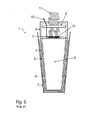
typical detector arrangement 1 is shown inFigure 5 . Such a detector arrangement can be used, for example, in high-energy physics. - The
conventional detector arrangement 1 essentially consists of ascintillator crystal 2 and an associatedsilicon photodiode 3 in the form of a pixelated avalanche photodetector operated in the Geiger-mode. In this embodiment, thescintillator crystal 2 consists of caesium iodide doped with thallium, i.e. CsI(T1). Further, thescintillator crystal 2 is wrapped with a diffusewhite reflector fabric 4 made of TyvecⓇ to catch light that has left thescintillator crystal 2 at its side surfaces. Further, thescintillator crystal 2 is wrapped in analuminum foil 5 constituting a radio frequency shielding. Moreover, thescintillator crystal 2 is wrapped in a MylarⓇfoil 6 providing an electrical insulation. Finally, theentire detector arrangement 1 is housed in acompartment 7 made of carbon fibre-reinforced carbon (CFC) providing mechanical support. Thephotodiode 3 is housed in analuminum frame 8 which is also housing apreamplifier board 9. Thesilicon photodiode 3 is arranged on adiode carrier plate 10 and there is anoutput cable 11 and a fibreoptical cable 12 connected to a light pulser. - However, it should be noted that the
conventional detector arrangement 1 as shown inFigure 5 merely comprises asingle scintillator crystal 2 and the associatedphotodiode 3. Therefore, the detector ring assembled from theconventional detector arrangements 1 merely comprises a single layer of thescintillator crystals 2. Hence, the detection performance of these conventional detector arrangements and the corresponding detector rings is unsatisfactory. - It is therefore an object of the invention to provide an improved detector arrangement and a corresponding detector ring for a tomographic imaging apparatus, particularly for a positron emission tomograph.
- Further, it is an object of the invention to provide an operating method for the detector ring according to the invention providing an improved detection performance.
- Preferably, the detector comprises a high granularity and also a high efficiency. Further, the detector preferably comprises an excellent position and time resolution.
- The invention is based on the idea that some of the Gamma photons generated by the positron-electron annihilations are Compton-scattered in the detector ring, which results in a primary photon detection and a secondary photon detection both having an energy of less than the annihilation energy of 511 keV. Therefore, these less energetic primary photon detections are discarded in conventional PETs although they are caused by positron-electron annihilations.
- Therefore, the detector arrangement according to the invention comprises at least two sandwiched pairs of a scintillator (e.g. an inorganic scintillator crystal) and an associated photodetector, e.g. a multi-pixel photo counter (MPPC) or a silicon photomultiplier (SiPM), wherein the pairs are sandwiched along a direction of detection, so that the corresponding detector ring comprises several layers of scintillators and the associated photodetectors. Therefore, the detector ring according to the invention is suitable for detecting Compton-scattered Gamma photons thereby improving the detection performance.
- In a preferred embodiment, the detector arrangement comprises three sandwiched pairs of a scintillator and an associated photodetector, wherein the pairs are sandwiched along a direction of detection. However, the invention is not restricted to a specific number of layers of scintillators in the detector ring. For example, detector rings with two, four, five or six layers of scintillators are possible.
- Further, it should also be noted that the detector arrangement preferably tapers along its direction of detection so that a plurality of detector arrangements can be assembled to form a detector ring without any optically inactive gaps between the adjacent detector arrangements. In the preferred embodiments, the scintillators therefore comprise a cross section in the form of a trapezoid or a hexagon.
- Further, the detector arrangement according to the invention preferably comprises an optical insulation for optically insulating the detector arrangement from an adjacent detector arrangement in a detector ring which is assembled from a plurality of the detector arrangements. The optical insulation between the adjacent detector arrangements avoids crosstalk between the adjacent detector arrangements.
- The optical insulation between the adjacent detector arrangements preferably comprises a diffuse reflector on the opposing side surfaces of the scintillators. For example, a diffusely reflecting white paint can be applied onto the opposing side surfaces of the scintillators to provide the optical insulation. Alternatively, the optical insulation can be provided by a cladding made of a fabric, particularly a fabric made of TyvekⓇ. Further, the optical insulation between the adjacent detector arrangements can be provided by an enhanced roughness of the opposing side surfaces of the scintillators so that the light is trapped within the scintillator. Finally, the optical insulation can be provided by nanocrystals on the opposing side surfaces of the scintillators. However, the invention is not restricted to the afore-mentioned techniques for providing the optical insulation between the adjacent detector arrangements in the detector ring.
- Further, the side surfaces of the scintillators preferably comprise an optical pattern (e.g. black spots) which homogenizes the response of the scintillators. The afore-mentioned optical pattern for homogenizing the response of the scintillators is preferably arranged between the scintillators and the optical insulation.
- It should further be noted that the individual scintillators preferably comprise a front face of 4 mm2 ± 0.2 mm2 on the receiving side. Moreover, the length of the entire detector arrangement is preferably 4.8 cm ± 0.5 cm, while the length of the individual scintillators is preferably 1.6 cm ± 0.2 mm or 1.4 cm ± 0.4 mm. However, the invention is not restricted to the afore-mentioned exemplary dimensions.
- It should further be noted that different types of photodetectors can be used in the framework of the invention. In a preferred embodiment of the invention, the photodetectors associated to the individual scintillators are pixelated avalanche photodiodes (APDs) operated in the Geiger-mode, e.g. silicon photo multipliers (SiPMs), multi-pixel photo counters (MPPCs) or pixelated semiconductor photodetectors. Finally, it is preferred to use a photodetector which is insensitive to magnetic fields, for example an avalanche photodiode operated in the Geiger mode. However, the invention is not restricted to the afore-mentioned types of photodetectors.
- Further, the scintillators are preferably scintillator crystals, particularly inorganic scintillator crystals. For example, the following inorganic scintillator crystals can be used in the framework of the invention: Lutetium orthosilicate (LSO), lutetium-yttrium orthosilicate (LSYO), barium fluoride BaF2), lead tungstate (PbWO4), bismuth germanate (BGO), caesium iodide (CsI), caesium iodide doped with thallium (CsI(T1)), sodium iodide doped with thallium (NaI(T1)), lanthanum-(III)-bromide (LaBr3) or lutetium-yttrium aluminum perovskite (LUYAP).
- Alternatively, it is possible to use organic scintillators having a shorter decay time facilitating a run time calculation thereby improving the detection performance.
- Therefore, at least one of the scintillators preferably may comprise a shorter decay time than the other scintillators thereby facilitating a precise run-time calculation. In a three-layer arrangement, two of the scintillators may consist of inorganic scintillator crystals while the other scintillator is an organic scintillator having a shorter decay time thereby facilitating a precise run-time calculation. For example, the decay time of the inorganic scintillators is typically longer than 20 ns while the shorter decay time of the organic scintillators is typically less than 5 ns.
- It should further be noted that the individual detector arrangements are preferably inserted in corresponding slots of a box which is preferably made of carbon-fibre. These boxes can be closed with a plate holding the individual photodetectors for the scintillators in the slots. For example, each of the boxes can have a size of 1 cm x 1 cm in the first layer and follows the projective geometry in the azimuthal direction and/or in the polar direction. Further, each box may include 25 crystals which are inserted in the slots of the box. However, the invention is not restricted to the afore-mentioned numbers of slots and dimensions.
- Moreover, it should be noted that the invention is not restricted to the individual detector arrangements as disclosed above. The invention rather comprises a complete detector ring for a tomographic imaging apparatus, particularly for a positron emission tomograph, comprising a plurality of the afore-mentioned detector arrangements being arranged along the circumference of the detector ring so that the detector ring consists of several layers of scintillators and associated photodetectors.
- The detector ring according to the invention preferably has an inner diameter of 60-100 cm and an axial length of 100 cm or more for a full-body PET. However, in case of a small PET, the axial length is preferably in the range of 5-50 cm having a diameter of preferably 30-60cm.
- It should further be noted that the individual detector arrangements in the detector ring are preferably projective with regard to an azimuth angle of the detector ring. In other words, the individual detector arrangements each comprise an optical axis wherein the optical axes of all detector arrangements intersect in the middle of the detector ring, i.e. on the centre axis of the detector ring.
- In case of a full-body PET with an axial length of 100 cm or more, the individual detector arrangements are preferably projective with regard to a polar angle of the detector ring. In other words, the individual detector arrangements are preferably angled with regard to a cross section of the detector ring so that the optical axes of all detector arrangements intersect substantially in the same cross section of the detector ring.
- Moreover, the invention encompasses a complete tomographic imaging apparatus, particularly a positron emission tomograph, comprising the afore-mentioned detector ring.
- Finally, the invention also encompasses a novel operating method for a tomographic imaging apparatus, particularly for a positron emission tomograph. The novel operating method according to the invention facilitates the detection of Compton-scattered Gamma photons thereby improving the detection performance of the tomographic imaging apparatus. Due to the small crystal sizes the compton scattered photons are more precisely determined.
- In conventional positron emission tomographs, the positions and energies of diametrically opposite primary photon detections are determined and the positions of the diametrically opposite primary photon detections are saved for a later image analysis if both diametrically opposite primary photon detections comprise a predetermined annihilation energy of typically 511 keV. However, if the photon detections comprise a lower energy due to Compton-scattering, the corresponding positions are discarded and not used for the later image analysis.
- However, the operating method according to the invention also determines the positions and energies of secondary photon detections caused by Compton-scattering of the less energetic primary photon. In other words, if one of the primary photon detections comprises the specific annihilation energy of typically 511 keV, while the other primary photon detection comprises a lower energy due to Compton-scattering, the position and energy of the secondary photon detection is determined.
- If the less energetic primary photon detection and the secondary photon detection comprise a total energy corresponding to the specific annihilation energy of typically 511 keV, the positions of the primary photon detections are saved for a later image analysis. In such a case, it is clear that the less energetic secondary photon detection was caused by Compton-scattering of the primary photon.
- However, if the total energy of the more energetic primary photon detection and the secondary photon detection does not correspond to the annihilation energy of typically 511 keV, it cannot be concluded that the secondary photon detection was caused by Compton-scattering of the primary photon. In such a case, the positions of the primary photon detections are discarded so that they are not used for image analysis.
- In a preferred embodiment of the invention, the operating method also considers events in which both primary photon detections comprise an energy of less than the specific annihilation energy of typically 511 keV. In such a case, it is determined whether there are any secondary photon detections having an energy matching with the energy of the primary photon detections in such a way that the sum of the energies corresponds to the specific annihilation energy of typically 511 keV. In such a case, the positions of the primary photon detections are saved for a later image analysis.
- It should further be noted that the search for the secondary photon detections is preferably restricted to a specific region in which the secondary photon detections are to be expected according to the energy of the corresponding primary photon detection. The multi-layer and highly granular structure allows for a precise detection of the compton scattered photons. In this connection it should be noted that the Compton-scattering angle corresponds to the difference between the specific annihilation energy on the one hand and the energy of the primary photon detection on the other hand. Therefore, noise related misdetections can be avoided by restricting the search to a specific region corresponding to the Compton-scattering angle. Specifically, the Compton-scattering angle is calculated based on the energy difference between the energy of the primary photon detection and the specific annihilation energy of typically 511 keV. Then, a cone is determined surrounding the flight path of the less energetic primary photon before its detection, wherein the cone corresponds to the Compton-scattering angle. Then, the search for the secondary photon detection is restricted to the cone.
- In the preferred embodiment of the invention, the apparatus is calibrated without a patient by inserting a source of radiation and measuring data. The source of radiation used for calibrating the apparatus is preferably a point source, e.g. a Natrium-22 source. However, other source of radiation can be used in the framework of the invention, e.g. Caesium-137, Sodium-22, Cobalt-57, Tin-113 or Barium-133. Further, the invention is not restricted to the afore-mentioned examples of radiation sources.
- The pixelated APDs operated in the Geiger mode are non linear devices that saturate at the maximum number of pixels available. For good energy measurements one needs to correct for this non-linearity. The non-linearity correction is preferably obtained from the saturation curves. The exact saturation curve needs to be measured for every photodetector. The saturation curves are voltage and temperature dependent. Thus, the calibration system needs to have the ability to measure the saturation at any time. It is proposed to accomplish this with several X-ray sources of fixed energy, e.g. Caesium-137 (662 keV), Sodium-22 (511 keV), Cobalt-57 (122 KeV), Tin-113 (392 keV + X rays) or Barium-133 (356 keV, 0.081 keV). LED's would be another possibility.
- In addition to the source calibration, one needs to perform a gain calibration. This is achieved by measuring the distance between the first pixel peak and the pedestal. Typically random triggers with noise hits can be used here. In processing electronics of the signal one needs a preamplifier with two different amplifications, a high amplification for the gain calibration to obtain the highest precision and low amplification for normal operations to achieve the highest dynamic range. The two amplification scales need to be cross calibrated. Here, one can use a gamma source such as Cobalt-57, which emits a 122-keV photon, and measure the response with the two amplification scales of the preamplifier. (The energy of the photon needs to be sufficiently smaller than 511 keV, so it falls into the dynamic range of the two preamplifier settings).
- Moreover, the light yield of the scintillators and the gain of the detector are affected temperature and voltage changes. Therefore, the power supply of the tomography apparatus is preferably stabilized in order to avoid variations in the light yield of the scintillators and the gain of the detector.
- Finally, it should be noted that the images generated by the positron emission tomography apparatus according to the invention can be combined with images generated by other tomography techniques, e.g. magnetic resonance imaging (MRI) or computer tomography (CT).
- The invention and its particular features and advantages will become more apparent from the following detailed description considered with reference to the accompanying drawings.
-
- Figure 1A
- is a schematic view of a cross section of a multi-layer detector ring according to the invention.
- Figure 1B
- is a longitudinal sectional view of the detector ring of
Figure 1A . - Figure 1C
- is an illustration showing primary photon detections only.
- Figure 1D
- is an illustration showing primary photon detections and secondary photon detections caused by Compton-scattering.
- Figure 2
- is a schematic side view of a detector arrangement comprising three pairs of a scintillator and an associated photodetector.
- Figure 3A
- is a perspective view of another detector ring.
- Figure 3B
- is a longitudinal sectional view of the detector ring of
Figure 3A . - Figure 4A-4C
- are flowcharts illustrating the operating method according to the invention.
- Figure 5
- shows a conventional detector arrangement according to the prior art.
-
Figures 1A-1D illustrate adetector ring 13 surrounding a patient 14 on apatient bed 15, wherein thedetector ring 13 comprises threelayers scintillator crystals 19 and associated photodetectors, wherein the photodetectors are pixelated avalanche photodetectors operated in the Geiger-mode. -
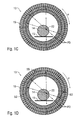
Figure 1C illustrates a positron-electron annihilation 20 within thepatient 14 resulting in the generation of a pair of Gamma photons which are irradiated in opposing directions. Further, the drawing shows primary photon detections PD in the individual layers 16-18 of the detector rings 13, i.e. photon detections with an energy corresponding to the annihilation energy of 511 keV. - Further,
Figure 1D illustrates both primary photon detections PD and secondary photon detections SD caused by Compton-scattering in theinner layers detector ring 13. It has to be noted that the Gamma photons generated by the positron-electron annihilation 20 in thepatient 14 are Compton-scattered in theinner layer 18 and also in themiddle layer 17 of thedetector ring 13 so that the corresponding primary photon detections PD indicate an energy of less than the specific annihilation energy of 511 keV. However, the energy of the secondary photon detections SD is measured and it is determined whether the sum of the energies of the primary photon detection PD and the associated secondary photon detection SD corresponds to the specific annihilation energy of 511 keV. If so, the positions of the primary photon detections PD are saved for a later image analysis which can be performed in conventional manner. -
Figure 2 shows a schematic illustration of adetector arrangement 21, comprising three pairs of a scintillator crystal 22-24 and an associated avalanche photodiode 25-27. - The
detector ring 13 as shown inFigures 1A-1D is assembled from a plurality of thedetector arrangements 21. In this connection it should be noted that the scintillator crystals 22-24 have a cross section in the form of a trapezoid so that there are no optically inactive gaps between theadjacent detector arrangements 21 in thedetector ring 13. - It should further be noted that an optical pattern comprising black spots in well-defined positions is painted on the side surfaces of the scintillator crystals 22-24 of the
detector arrangements 21 thereby homogenizing the response of the scintillator crystals 22-24. - Further, a white diffuse reflector layer is painted onto the side surfaces of the scintillator crystals 22-24 thereby providing an optical insulation between the
adjacent detector arrangements 21 in the detector ring. - In this embodiment, the individual scintillator crystals 22-24 each has a length of L = 1.6 cm. However, other arrangements with different dimensions are possible within the framework of the invention.
-
Figure 3A shows an alternative embodiment of adetector ring 28 comprising a plurality ofdetector arrangements 29 which are distributed both along the circumference of thedetector ring 28 and along the length of thedetector ring 28. - The
individual detector arrangements 29 each comprise three pairs of a scintillator crystal and an associated photodetector in the form of a pixelated avalanche photodetector operated in the Geiger-mode. - Further, it should be noted that the
individual detector arrangements 29 are projective with regard to an azimuth angle of thedetector ring 28, i.e. theindividual detector arrangements 29 compriseoptical axes 30 intersecting acentre axis 31 of the detector ring. However, the detectors can also be projective in the polar direction. - Moreover, the
optical axes 30 of thedetector arrangements 29 intersect in the same cross section 32 of thedetector ring 28. - Finally,
Figures 4A-4C illustrate the operating method according to the invention, wherein steps S1-S4 as shown inFigure 4A are performed in conventional positron emission tomography apparatuses, whereas steps S5-S22 as shown inFigures 4B and 4C are improvements of the invention over the state of the art. - In step S1, the energy and position of primary photon detections in the detector ring is measured.
- Then, in step S2, it is determined whether there are two diametrically opposite primary photon detections indicating that the corresponding Gamma photons stem from a positron-electron annihilation.
- If so, it is determined in step S3 whether the energy of both opposite photon detections corresponds to the annihilation energy of 511 keV.
- If so, the positions of both primary photon detections are saved in step S4 for a later image analysis which can be performed in a conventional manner.
- Otherwise, it is determined in step S5 whether only one of the opposite primary photon detections comprises the annihilation energy of 511 keV.
- If so, the corresponding Compton-scattering angle is calculated from the energy of the less energetic primary detection in step S6. In this connection, it should be noted that the Compton-scattering angle is related to the energy difference between the annihilation energy on the one hand and the energy of the primary photon detection on the other hand.
- Then, in step S7 a secondary photon detection is searched on a cone comprising the calculated Compton-scattering angle.
- In step S8, it is determined whether there is a secondary photon detection on the cone.
- If so, step S9 calculates the sum of the energies of the less energetic primary photon detection and the secondary photon detection on the cone.
- In step S10, it is determined whether the sum of these energies corresponds to the annihilation energy of 511 keV ±60 keV.
- If so, the positions of the primary photon detections are saved in step S11 for a later image analysis.
- Otherwise, the primary photon detections are discarded in step S12 since they are probably not caused by a positron-electron annihilation.
- However, if none of the primary photon detections comprises the specific annihilation energy of 511 keV, the Compton-scattering angle is determined for both less energetic primary photon detections (steps S13, S16) and it is searched for a secondary photon detection on a cone with the scattering angle (steps S14, S17).
- If two secondary photon detections occur on the cones corresponding to the calculated Compton-scattering angles, step S19 calculates the total sum of the energies of the primary photon detections and the secondary photon detections.
- In step S20, it is determined whether the sum of these energies equals the double of the specific annihilation energy of 511 keV ±60 keV.
- If so, the positions of the primary photon detections are saved in step S21 for a later image analysis.
- Otherwise, the primary photon detections are discarded in step S22.
- Although the invention has been described with reference to the particular arrangement of parts, features and the like, these are not intended to exhaust all possible arrangements of features, and indeed many other modifications and variations will be ascertainable to those of skill in the art.
-
- 1
- Detector arrangement
- 2
- Scintillator crystal
- 3
- Photodiode
- 4
- Reflector fabric
- 5
- Aluminum foil
- 6
- Mylar foil
- 7
- Compartment
- 8
- Frame
- 9
- Preamplifier board
- 10
- Diode carrier plate
- 11
- Output cable
- 12
- Fibre optical cable
- 13
- Detector ring
- 14
- Patient
- 15
- Patient bed
- 16-18
- Layers
- 19
- Scintillator crystal
- 20
- Positron-electron annihilation
- 21
- Detector arrangement
- 22-24
- Scintillator crystal
- 25-27
- Pixelated avalanche photodiode operated in the Geiger mode
- 28
- Detector ring
- 29
- Detector arrangements
- 30
- Optical axes of the detector arrangements
- 31
- Centre axis
- 32
- Cross section of the detector ring
- PD
- Primary photon detection
- SD
- Secondary photon detection
Claims (18)
- Detector arrangement (21; 29) for a tomographic imaging apparatus, particularly for a positron emission tomograph, characterized by at least two sandwiched pairs of a scintillator (22-24) and an associated pixelated avalanche photodetector (25-27) operated in the Geiger-mode, wherein the pairs are sandwiched along a direction of detection.
- Detector arrangement (21; 29) according to claim 1, whereina) the detector arrangement (21; 29) tapers along its direction of detection so that a plurality of the detector arrangements (21; 29) can be assembled to form a detector ring (13; 28) without any optically inactive gaps between the adjacent detector arrangements, and/orb) the scintillators (22-24) each comprises a cross section in the form of a trapezoid or a hexagon, and/orc) the detector arrangement comprises a high granularity.
- Detector arrangement (21; 29) according to one of the preceding claims, characterized by an optical insulation for optically insulating the detector arrangement (21; 29) from an adjacent detector arrangement (21; 29) in a detector ring (13; 28) which is assembled from a plurality of the detector arrangements (21; 29).
- Detector arrangement (21; 29) according to claim 3, wherein the optical insulation comprises a diffuse reflector on the opposing side surfaces of the scintillators (22-24).
- Detector arrangement (21; 29) according to claim 3 or claim 4, wherein the optical insulation comprisesa) a diffusely reflecting paint on the opposing side surfaces of the scintillators, and/orb) a cladding made of a fabric, particularly a fabric made of Tyvek Ⓡ, and/orc) an enhanced surface roughness of the opposing side surfaces of the scintillators, and/ord) nanocrystals on the opposing side surfaces of the scintillators.
- Detector arrangement (21; 29) according to one of the preceding claims, wherein the side surfaces of the scintillators (22-24) comprise an optical pattern which homogenizes the response of the scintillators (22-24).
- Detector arrangement (21; 29) according to claim 6, whereina) the optical pattern comprises a surface treatment to achieve a uniform response, particularly in the form of black spots, and/orb) the optical pattern is arranged between the scintillators (22-24) and the optical insulation.
- Detector arrangement (21; 29) according to one of the preceding claims, whereina) at least one of the scintillators (22-24) may comprise a shorter decay time than the other scintillators (22-24) thereby facilitating a precise run-time calculation, and/orb) the inner scintillators (22) may comprise a shorter decay time than the outer scintillators (24) in order to reduce the coincidence time between the back-to-back annihilation photons and to improve the position determination of their production point, and/orc) the shorter decay time of the scintillators (22-24) is less than 5ns, particularly about 1ns, and/ord) the longer decay time of the scintillators (22-24) is more than 20ns, particularly in the range of 20ns-50ns.
- Detector ring (13; 28) for a tomographic imaging apparatus, particularly for a positron emission tomograph, comprising several detector arrangements (21; 29) according to one of the preceding claims being arranged along the circumference of the detector ring (13; 28) so that the detector ring (13; 28) comprises several layers of scintillators (22-24) and associated photodetectors (25-27).
- Detector ring (13; 28) according to claim 9, whereina) the individual detector arrangements (21; 29) are projective with regard to an azimuth angle (φ) of the detector ring (13; 28), and/orb) the individual detector arrangements (21; 29) may be projective with regard to a polar angle (θ) of the detector ring (13; 28).
- Tomographic imaging apparatus, particularly for a positron emission tomograph, comprising a detector ring (13; 28) according to one of claims 9 or 10.
- Operating method for a tomographic imaging apparatus, particularly for a positron emission tomograph, comprising the following steps:a) Determining the positions and energies of diametrically opposite primary photon detections (PD), wherein the determination is made by means of a pixelated avalanche photodetector operated in the Geiger-mode,b) saving the positions of the diametrically opposite primary photon detections (PD) for a later image analysis if both diametrically opposite primary photon detections (PD) comprise a predetermined annihilation energy,
characterized by the following steps which are performed if only one of the diametrically opposite photon detections comprises the predetermined annihilation energy:c) Determining the positions and energies of secondary photon detections (SD) caused by Compton-scattering of the less energetic primary photon, wherein the determination is made by means of a pixelated avalanche photodetector operated in the Geiger-mode, particularly by a multi-pixel photo counter or by a silicon photomultiplier,d) saving the positions of the diametrically opposite primary photon detections (PD) if the sum of the energies of the less energetic primary photon detection (PD) and the secondary photon detection (SD) equals the predetermined annihilation energy. - Operating method according to claim 12, further comprising the following steps which are performed if none of the diametrically opposite primary photon detections (PD) comprises the predetermined annihilation energy:a) Determining the positions and energies of secondary photon detections (SD) caused by Compton-scattering of both primary photons,b) calculating the total sum of the energies of both primary photon detections (PD) and both secondary photon detections (SD) ,c) saving the positions of the diametrically opposite primary photon detections (PD) if the total sum of the energies equals the double of the predetermined annihilation energy.
- Operating method according to claims 12 or 13, further comprising the following steps for determining the secondary photon detections (SD):a) Calculating an energy difference between the predetermined annihilation energy on the one hand and the energy of the primary photon detection (PD) having an energy different from the predetermined annihilation energy on the other hand,b) calculating a Compton-scattering angle based on the energy difference,c) Determining a cone surrounding the flight path of the less energetic primary photon before its detection wherein the cone corresponds to the Compton-scattering angle,d) Searching for the secondary photon detection (SD) on the cone only.
- Operating method according to one of claims 12 to 14, further comprising the following steps:Calibrating the apparatus without a patient by inserting a source of radiation and measuring data.
- Operating method according to claim 15, comprising the following steps:a) Measuring saturation curves of the pixelated avalanche photodetector for different ambient temperatures and/or different sources of radiation,b) Saving the measured saturation curves of the pixelated avalanche photodetector,c) Use of the tomographic imaging apparatus for examining a patient,d) Correction of the measurements of the patient taking into account the saturation curves.
- Operating method according to claim 16, wherein the different radiation sources are selected from a group consisting of:a ) 137Caesium,b) 22Sodium,c) 57Cobalt,d) 113Tin,e) 133Barium
- Operating method according to one of claims 12 to 15, further comprising the following step:a) Measuring an ambient temperature and considering the ambient temperature to avoid temperature variations of the light yield of the scintillators and/or the gain of the avalanche photodetector, and/orb) Stabilizing a power supply of the tomography apparatus to avoid variations of the gain of the avalanche photodetector, and/orc) Adjusting a bias voltage automatically due to temperature changes to ensure operation at the same gain..
Priority Applications (2)
| Application Number | Priority Date | Filing Date | Title |
|---|---|---|---|
| EP10001529A EP2360493A1 (en) | 2010-02-15 | 2010-02-15 | Detector arrangement for a tomographic imaging apparatus, particularly for a positron emission tomograph |
| US13/025,341 US20110198504A1 (en) | 2010-02-15 | 2011-02-11 | Detector arrangement for a tomographic imaging apparatus, particularly for a positron emission tomograph |
Applications Claiming Priority (1)
| Application Number | Priority Date | Filing Date | Title |
|---|---|---|---|
| EP10001529A EP2360493A1 (en) | 2010-02-15 | 2010-02-15 | Detector arrangement for a tomographic imaging apparatus, particularly for a positron emission tomograph |
Publications (1)
| Publication Number | Publication Date |
|---|---|
| EP2360493A1 true EP2360493A1 (en) | 2011-08-24 |
Family
ID=42338983
Family Applications (1)
| Application Number | Title | Priority Date | Filing Date |
|---|---|---|---|
| EP10001529A Withdrawn EP2360493A1 (en) | 2010-02-15 | 2010-02-15 | Detector arrangement for a tomographic imaging apparatus, particularly for a positron emission tomograph |
Country Status (2)
| Country | Link |
|---|---|
| US (1) | US20110198504A1 (en) |
| EP (1) | EP2360493A1 (en) |
Cited By (6)
| Publication number | Priority date | Publication date | Assignee | Title |
|---|---|---|---|---|
| WO2014012182A1 (en) * | 2012-07-19 | 2014-01-23 | University Of Saskatchewan | Pet and spect multi photon imaging with single radioactive isotopes |
| GB2522017A (en) * | 2014-01-08 | 2015-07-15 | Symetrica Ltd | Apparatus and methods for gamma ray detection |
| US9164144B2 (en) | 2012-12-27 | 2015-10-20 | General Electric Company | Characterization and calibration of large area solid state photomultiplier breakdown voltage and/or capacitance |
| US9606245B1 (en) | 2015-03-24 | 2017-03-28 | The Research Foundation For The State University Of New York | Autonomous gamma, X-ray, and particle detector |
| CN108562928A (en) * | 2017-12-18 | 2018-09-21 | 中派科技(深圳)有限责任公司 | Detector and Positron emission tomography equipment for Positron emission tomography equipment |
| WO2020063232A1 (en) * | 2018-09-30 | 2020-04-02 | 中派科技(深圳)有限责任公司 | Pet device, multilayer crystal pet detector, and electronic reading module and method therefor |
Families Citing this family (17)
| Publication number | Priority date | Publication date | Assignee | Title |
|---|---|---|---|---|
| US8017915B2 (en) | 2008-03-14 | 2011-09-13 | Reflexion Medical, Inc. | Method and apparatus for emission guided radiation therapy |
| JP5851733B2 (en) * | 2011-06-24 | 2016-02-03 | 浜松ホトニクス株式会社 | PET apparatus and radiation detector unit |
| WO2014020471A2 (en) | 2012-07-30 | 2014-02-06 | Koninklijke Philips N.V. | High spatial resolution mode solid state positron emission tomography (pet) scanner |
| US9310491B2 (en) * | 2012-09-27 | 2016-04-12 | Schlumberger Technology Corporation | Scintillator with tapered geometry for radiation detectors |
| DE102013216197A1 (en) * | 2013-08-14 | 2015-02-19 | Berthold Technologies Gmbh & Co. Kg | Method for operating a radiometric measuring system and radiometric measuring system |
| US9541656B2 (en) | 2013-12-20 | 2017-01-10 | General Electric Company | System and method for compensating temperature gain variation in radiation detectors |
| CN104688260A (en) * | 2015-03-19 | 2015-06-10 | 明峰医疗系统股份有限公司 | Embedded PET-CT synchronous scanning device based on SiPM |
| WO2018093933A1 (en) | 2016-11-15 | 2018-05-24 | Reflexion Medical, Inc. | System for emission-guided high-energy photon delivery |
| WO2018183748A1 (en) | 2017-03-30 | 2018-10-04 | Reflexion Medical, Inc. | Radiation therapy systems and methods with tumor tracking |
| CN107080551B (en) * | 2017-05-25 | 2023-08-22 | 苏州瑞派宁科技有限公司 | Three-dimensional heterogeneous PET system |
| CN114699655A (en) | 2017-07-11 | 2022-07-05 | 反射医疗公司 | Method for persistence management of PET detectors |
| CN111148471B (en) | 2017-08-09 | 2023-08-22 | 反射医疗公司 | System and method for fault detection in emission guided radiation therapy |
| US11369806B2 (en) | 2017-11-14 | 2022-06-28 | Reflexion Medical, Inc. | Systems and methods for patient monitoring for radiotherapy |
| CN108508474B (en) * | 2018-01-31 | 2022-01-21 | 中派科技(深圳)有限责任公司 | Detector for positron emission imaging apparatus and positron emission imaging apparatus |
| JP7293334B2 (en) * | 2018-08-07 | 2023-06-19 | シーメンス メディカル ソリューションズ ユーエスエー インコーポレイテッド | Nearly 2π Compton camera for medical imaging |
| CN109009198B (en) * | 2018-08-21 | 2020-05-19 | 北京科技大学 | Multi-modality imaging system, method, and storage medium |
| EP4127777A1 (en) * | 2020-05-01 | 2023-02-08 | Siemens Medical Solutions USA, Inc. | Transmission imaging in a pet scanner based on forward-scattered gamma rays with coincidence detection |
Citations (4)
| Publication number | Priority date | Publication date | Assignee | Title |
|---|---|---|---|---|
| US4291228A (en) * | 1979-06-19 | 1981-09-22 | Montreal Neurological Institute | Detector shape and arrangement for positron annihilation imaging device |
| US4647779A (en) * | 1985-05-13 | 1987-03-03 | Clayton Foundation For Research | Multiple layer positron emission tomography camera |
| US20050167599A1 (en) * | 2003-10-16 | 2005-08-04 | Schlyer David J. | Positron emission tomography wrist detector |
| US20070194242A1 (en) * | 2003-11-25 | 2007-08-23 | Koninklijke Philips Electronics Nv | Scintillation Layer For A Pet-Detector |
Family Cites Families (6)
| Publication number | Priority date | Publication date | Assignee | Title |
|---|---|---|---|---|
| US3978337A (en) * | 1975-01-29 | 1976-08-31 | Wisconsin Alumni Research Foundation | Three-dimensional time-of-flight gamma camera system |
| US5514870A (en) * | 1994-03-11 | 1996-05-07 | James R. Langenbrunner | Fast CsI-phoswich detector |
| JP2000321357A (en) * | 1999-03-10 | 2000-11-24 | Toshiba Corp | Nuclear medicine diagnostic device |
| US7834321B2 (en) * | 2006-07-14 | 2010-11-16 | Carestream Health, Inc. | Apparatus for asymmetric dual-screen digital radiography |
| US7488943B2 (en) * | 2006-07-17 | 2009-02-10 | General Electric Company | PET detector methods and apparatus |
| US20100268074A1 (en) * | 2008-07-02 | 2010-10-21 | Radiation Monitoring Devices, Inc. | Strontium halide scintillators, devices and methods |
-
2010
- 2010-02-15 EP EP10001529A patent/EP2360493A1/en not_active Withdrawn
-
2011
- 2011-02-11 US US13/025,341 patent/US20110198504A1/en not_active Abandoned
Patent Citations (4)
| Publication number | Priority date | Publication date | Assignee | Title |
|---|---|---|---|---|
| US4291228A (en) * | 1979-06-19 | 1981-09-22 | Montreal Neurological Institute | Detector shape and arrangement for positron annihilation imaging device |
| US4647779A (en) * | 1985-05-13 | 1987-03-03 | Clayton Foundation For Research | Multiple layer positron emission tomography camera |
| US20050167599A1 (en) * | 2003-10-16 | 2005-08-04 | Schlyer David J. | Positron emission tomography wrist detector |
| US20070194242A1 (en) * | 2003-11-25 | 2007-08-23 | Koninklijke Philips Electronics Nv | Scintillation Layer For A Pet-Detector |
Non-Patent Citations (1)
| Title |
|---|
| QINGGUO XIE ET AL: "Performance evaluation of multi-pixel photon counters for PET imaging", NUCLEAR SCIENCE SYMPOSIUM CONFERENCE RECORD, 2007. NSS '07. IEEE, IEEE, PI, 1 October 2007 (2007-10-01), pages 969 - 974, XP031206643, ISBN: 978-1-4244-0922-8 * |
Cited By (10)
| Publication number | Priority date | Publication date | Assignee | Title |
|---|---|---|---|---|
| WO2014012182A1 (en) * | 2012-07-19 | 2014-01-23 | University Of Saskatchewan | Pet and spect multi photon imaging with single radioactive isotopes |
| US9164144B2 (en) | 2012-12-27 | 2015-10-20 | General Electric Company | Characterization and calibration of large area solid state photomultiplier breakdown voltage and/or capacitance |
| GB2522017A (en) * | 2014-01-08 | 2015-07-15 | Symetrica Ltd | Apparatus and methods for gamma ray detection |
| GB2522017B (en) * | 2014-01-08 | 2017-09-20 | Symetrica Ltd | Apparatus and methods for gamma ray detection |
| US10429523B2 (en) | 2014-01-08 | 2019-10-01 | Symetrica Limited | Apparatus and methods for gamma ray detection |
| US9606245B1 (en) | 2015-03-24 | 2017-03-28 | The Research Foundation For The State University Of New York | Autonomous gamma, X-ray, and particle detector |
| US9835737B1 (en) | 2015-03-24 | 2017-12-05 | The Research Foundation For The State University Of New York | Autonomous gamma, X-ray, and particle detector |
| CN108562928A (en) * | 2017-12-18 | 2018-09-21 | 中派科技(深圳)有限责任公司 | Detector and Positron emission tomography equipment for Positron emission tomography equipment |
| CN108562928B (en) * | 2017-12-18 | 2022-01-21 | 中派科技(深圳)有限责任公司 | Detector for positron emission imaging apparatus and positron emission imaging apparatus |
| WO2020063232A1 (en) * | 2018-09-30 | 2020-04-02 | 中派科技(深圳)有限责任公司 | Pet device, multilayer crystal pet detector, and electronic reading module and method therefor |
Also Published As
| Publication number | Publication date |
|---|---|
| US20110198504A1 (en) | 2011-08-18 |
Similar Documents
| Publication | Publication Date | Title |
|---|---|---|
| EP2360493A1 (en) | Detector arrangement for a tomographic imaging apparatus, particularly for a positron emission tomograph | |
| US10955569B2 (en) | Detector systems for integrated radiation imaging | |
| US11079501B2 (en) | Advanced temperature compensation and control circuit for single photon counters | |
| US10365385B2 (en) | Apparatus, method and system for sparse detector | |
| EP1627239B1 (en) | A detector module for detecting ionizing radiation | |
| US10203419B2 (en) | Detector component for an X-ray or gamma ray detector | |
| US9271694B2 (en) | System and method of simplifying a direct control scheme for a detector | |
| US10466371B2 (en) | Apparatus and methods for depth-of-interaction positron tomography detector using dichotomous sensing | |
| KR101542836B1 (en) | Detector for Positron Emission Tomography and Positron Emission Tomography system using the same | |
| ES2629092A1 (en) | Compon gamma ray camera system with flight time measurement (Machine-translation by Google Translate, not legally binding) | |
| EP3109675B1 (en) | Pet detector modules utilizing overlapped light guides | |
| US8063377B2 (en) | Crystal identification for high resolution nuclear imaging | |
| EP3848980A1 (en) | Optical detector | |
| Jung et al. | Development of brain PET using GAPD arrays | |
| Wang et al. | Energy calibration using scintillator background radiation for high-resolution PET detectors | |
| JP6508343B2 (en) | Radiation detector and detector module | |
| Kataoka et al. | Development of an APD-based PET module and preliminary resolution performance of an experimental prototype gantry | |
| Stringhini et al. | Development of a high resolution module for PET scanners | |
| US20230236328A1 (en) | Method and apparatus for improved photosensor light collection in a radiation detector | |
| Wang et al. | Compact pixelated scintillator detector investigation for gamma ray detection | |
| Brasse et al. | Instrumentation Challenges in (S) PE (C) T Systems | |
| Lecomte | Molecular PET instrumentation and imaging techniques | |
| Saha | Pet scanning systems | |
| Castro et al. | Small prototype gamma camera based on wavelength-shifting fibres | |
| JP2009229336A (en) | Method and device for improving sensitivity of positron image |
Legal Events
| Date | Code | Title | Description |
|---|---|---|---|
| PUAI | Public reference made under article 153(3) epc to a published international application that has entered the european phase |
Free format text: ORIGINAL CODE: 0009012 |
|
| PUAI | Public reference made under article 153(3) epc to a published international application that has entered the european phase |
Free format text: ORIGINAL CODE: 0009012 |
|
| 17P | Request for examination filed |
Effective date: 20110311 |
|
| AK | Designated contracting states |
Kind code of ref document: A1 Designated state(s): AT BE BG CH CY CZ DE DK EE ES FI FR GB GR HR HU IE IS IT LI LT LU LV MC MK MT NL NO PL PT RO SE SI SK SM TR |
|
| AX | Request for extension of the european patent |
Extension state: AL BA RS |
|
| 17Q | First examination report despatched |
Effective date: 20140811 |
|
| STAA | Information on the status of an ep patent application or granted ep patent |
Free format text: STATUS: THE APPLICATION IS DEEMED TO BE WITHDRAWN |
|
| 18D | Application deemed to be withdrawn |
Effective date: 20141223 |