EP2337145A1 - Compact and adjustable power divider and filter device - Google Patents
Compact and adjustable power divider and filter device Download PDFInfo
- Publication number
- EP2337145A1 EP2337145A1 EP09290971A EP09290971A EP2337145A1 EP 2337145 A1 EP2337145 A1 EP 2337145A1 EP 09290971 A EP09290971 A EP 09290971A EP 09290971 A EP09290971 A EP 09290971A EP 2337145 A1 EP2337145 A1 EP 2337145A1
- Authority
- EP
- European Patent Office
- Prior art keywords
- input
- posts
- output
- input signal
- power
- Prior art date
- Legal status (The legal status is an assumption and is not a legal conclusion. Google has not performed a legal analysis and makes no representation as to the accuracy of the status listed.)
- Withdrawn
Links
Images


Classifications
-
- H—ELECTRICITY
- H01—ELECTRIC ELEMENTS
- H01P—WAVEGUIDES; RESONATORS, LINES, OR OTHER DEVICES OF THE WAVEGUIDE TYPE
- H01P1/00—Auxiliary devices
- H01P1/20—Frequency-selective devices, e.g. filters
- H01P1/213—Frequency-selective devices, e.g. filters combining or separating two or more different frequencies
- H01P1/2136—Frequency-selective devices, e.g. filters combining or separating two or more different frequencies using comb or interdigital filters; using cascaded coaxial cavities
-
- H—ELECTRICITY
- H01—ELECTRIC ELEMENTS
- H01P—WAVEGUIDES; RESONATORS, LINES, OR OTHER DEVICES OF THE WAVEGUIDE TYPE
- H01P5/00—Coupling devices of the waveguide type
- H01P5/12—Coupling devices having more than two ports
- H01P5/16—Conjugate devices, i.e. devices having at least one port decoupled from one other port
Definitions
- the invention relates to the field of microwave passive devices. It particularly relates to microwave multiplexers and power dividers.
- the received signal contains several communication channels multiplexed in frequency.
- receiver equipments In order to process each channel separately, receiver equipments generally comprise an Input Multiplexer (IMUX) device.
- IMUX Input Multiplexer
- the IMUX device function is to separate each frequency channel included in the input signal and to send each channel to a different output, so the signal corresponding to each of the channels can be processed separately.
- Figure 1 shows a typical block diagram of an IMUX device.
- Such a microwave device comprises an input channel and several separate output channels each of them consisting in a filter transmitting a signal with a limited bandwidth. Said bandwidth corresponds to that of the communication channel the output channel is supposed to transmit. To this purpose the filter is configured to limit the bandwidth of the input signal to that of the communication channel.
- each of the two groups substantially covers a half of the complete bandwidth.
- IMUX generally comprises a splitting input section comprising a filter associated to a power splitter/divider.
- the input section filter is intended to match the bandwidth of the input signal, while rejecting useless bands.
- the filtered input signal is then transmitted to the different communication channels.
- the power divider function splits an input signal into two outputs, each one with half the power of the input signal.
- Such a structure generally comprises two separate elements, a filtering element and a power splitting element, connected together by connection means.
- a drawback of such a configuration is that as the filter element and the splitter element are built and adjusted separately a further adjustment must be done when the two elements are connected together so as to realize the optimal adjustment of the complete structure. This optimal adjustment is important to minimize power loss and distortion of the input signal.
- microwave structures can be used to achieve this function with minimum power loss due to dissipation and mismatch and with minimum distortion of the input signal. These structures differ from the aforementioned ones in that they overlap the filtering function and the power dividing function. However, in such structures, the components performing each function are still clearly identifiable.
- One object of the invention is directed to providing an input section structure making it possible to overcome the drawbacks of the known structures used to make the input section of an Input Multiplexer.
- a more general object of the invention is to provide a structure able to combine in one and a same device a filtering and a splitting function. Another object is to provide an integrated signal divider/splitter structure able to produce from an input signal two signals of the same power with a strictly limited bandwidth whatever the bandwidth of the input signal could be. Another object of the invention is to provide an input function that can be controlled for the frequency behaviour as well as for the power balance.
- the subject of the invention is a power divider and filter in a single device, characterized in that it comprises one input and N outputs, and P coupled resonant elements, said device splitting an input signal into N different output signals with a given equal pre-designed and adjustable frequency bandwidth, the power of the input signal being shared between the output signals in a controllable manner.
- the device according to the invention comprises a case closed by a cover, said case including an inner space divided into six cavities by internal walls, said cavities communicating with one another by the means of apertures.
- Each cavity includes a metallic resonating post.
- One of the posts is configured to receive the input signal, while two other posts are configured to transmit a filtered output signal.
- the input signal is transmitted from the input to the separate outputs by coupling between the posts.
- the size and shape of the apertures and the distances between the posts is defined in order to obtain the desired bandwidth for the two output signals as well as to obtain the desired balance of the powers of these output signals.
- the post that is configured to receive the input signal as well as the two posts configured to transmit the two output signals have a parallelepipedic shape, while the other posts have a cylindrical shape.
- the input post and the two output posts are respectively linked to input or output ports.
- the cover comprise thread holes configured to receive power balance and bandwidth adjustment screws, said holes being arranged on the surface of the cover in order to face the posts or the apertures which separate the different cavities.
- the multiplexer device configured to split a signal received on an input port into several output signals each of them being transmitted to a separate output port, each output signal having a given bandwidth and a power level corresponding to a given part of the input signal power level.
- the multiplexer device comprises a power divider and filter device according to the invention which inputs are connected to the input of the multiplexer device, each of the two output signals produced by the power divider and filter device being transmitted to one of the two sets of output ports.
- the proposed input section device is an alternate improvement to current input sections.
- current input sections use different elements to realize the two different functions of an input section.
- FIG. 1 illustrates the functional diagram of an input multiplexer, IMUX, commonly used in telecommunication equipments (receivers).
- IMUX input multiplexer
- Such a device mainly comprises two parts, an input part consisting in the input section 12 which comprises an input port 121 and two output ports, 122 and 123, and an output part comprising two separate sets 15 and 16 of output channels.
- Each set of output channels 15 or 16 comprises itself an input port connected to one of the two output ports, 122 or 123, of the input section 12 and N output ports, 151 or 161, each port corresponding to one of the output channels of the IMUX device.
- Each output channel of an IMUX mainly comprises a band pass filter 17 the bandwidth of which corresponding to the bandwidth of one the communication channels. Moreover the bandwidths of the filters, ⁇ f 1 to ⁇ f 8 in the example, are generally configured so as to cover the whole communication bandwidth ⁇ F.
- the input section 12 mainly comprises an input two separate elements, a band pass filter 13 followed by a power splitter/divider 14.
- the band pass filter 13 is configured so as to match the whole communication bandwidth and strongly reject out-of-band signals.
- the power divider 14 generally shares out the input signal received by the input section in output signal, generally of the same power, each signal being sent to one of the two output ports of the section 12.
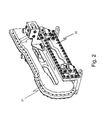
- Figure 2 illustrates a first example of device known of the prior art, achieving the input section function 12.
- the input section has wave guide structure comprising two separate coupled devices 21 and 22 in one and a same embodiment.
- Figure 3 illustrates a second example of device known of the prior art.
- the input section has a planar structure comprising two separate devices in one and a same embodiment.
- Said structure comprises a power divider main element 31, with a terminal part 32 corresponding to the two output ports 33 and 34 of the main element 31.
- the main element 31 has an initial part 35 where the input port 36 is connected, this port comprising a band pass filter at its beginning.
- both of the structures correspond to two different possible embodiments of an input section structure, each of them having its advantages and its drawbacks.
- both of the structures share the same drawback of achieving the splitting and filtering functions separately, function being implemented after the other.
- Figure 4 shows a schematic diagram illustrating the operating concept of the invention.
- Microwave filters are 2-port devices that show a frequency response according to some electrical requirements. Design methods generally take those requirements and construct an ideal mathematical response (typically a Chebyshev response) that corresponds to them. This ideal mathematical response can be then materialized by an electrical circuit with lumped components, based on resonators and couplers as illustrated on figure 4 .
- an ideal mathematical response typically a Chebyshev response
- the so designed circuit 41 comprises resonators elements 42, 43 and 44 coupled by positive or negative couplings to one another.
- Microwave resonators can be built using any existing known technology (coaxial resonators, cavity resonators, dielectric resonators ). Input and output circuits are as for them coupled to the device by some resonators 43 and 44 called port resonators.
- resonators 42 coupled to the port resonators 43 and 44 and coupled to one another, divide the electromagnetic energy produced by the input circuit illustrated by a generator e G and a resistor R G on figure 4 , and transmit it to the output circuit illustrated by a resistor R L .
- the frequency response of the device is given by its topology and depends on the coupling matrix of the equivalent electrical network.
- an analysis of the physical dimensions that determine the electrical properties of the microwave structure elements corresponding to those of the equivalent electrical circuit can be performed. This analysis can be done using any adequate known method. Such analysis advantageously makes it possible to relate the physical dimensions of the microwave structure elements used to build the desired device to the values of the corresponding elements of the equivalent electrical circuit.
- the structure so established can moreover be tested in an electromagnetic simulator and optimized the values of the different elements to match at best the desired characteristics.
- the characteristics of the different elements and their arrangement can be determined in order to build up, as a single device, a device comprising two identical filters with a common input, and two separate outputs, each filter delivering a filtered signal on the corresponding output and processing a signal which energy is equal to a half of the energy of the signal received at the common input.
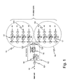
- Figure 6 shows a schematic view of the main structure of the device according to the invention in a particular embodiment given as an example. According to the invention this embodiment corresponds to a device implementing power splitting and frequency filtering in one and a same operation.
- the device according to the invention mainly comprises a main metallic cavity 61 partly divided by two internal metallic walls 67 in order to form six cavities 644, 645, 654, 655, 664 and 665. These cavities comprise resonating metallic posts 641, 642, 651, 652, 661 and 662, coupled to one another.
- metallic posts 641, 651 or 661 are connected to coaxial input/outputs 643, 653 and 663 of the device and have a parallelepiped shape.
- the other posts 642, 652 and 662 are cylindrical.
- the dimensions of the different cavities as well as the sizes of the metallic posts are determined, in a known manner, in relation to the frequency and the input power of the signal. As stated before, these determinations can be made using the methods aforementioned. In the other hand the distances between the different posts, as well as the sizes of the apertures between the posts, control the coupling between posts.
- the resonant post 651 is connected to the input signal by connection means providing a coaxial input 653.
- lateral resonant posts 641 and 661 provide each an output filtered signal which energy is of a half of that of the input signal.
- Output signals are delivered by the means of coaxial connection 643 and 663.
- an incoming signal propagates from the input coaxial line to the inner part of the filter through the first resonating post 651 which transmits it to resonating post 652, being the distance between both posts and the width of the aperture 656 the mechanism used to control the bandwidth.
- the signal transmitted by post 652 is split up into two parts, each part being transmitted to one of the two resonating posts 642 and 662, so defining two separate paths.
- the balance of the division is here controlled by apertures 647 and 667 that also match the desired bandwidth.
- signal passes from posts 642 and 662 to the two output resonating posts 641 and 661.
- distance is also the mechanism controlling the bandwidth.
- the desired bandwidth of the device is obtained by controlling the distance between the posts located in each of the cavities and the sizes of the apertures 656, 647 and 667 between the cavities. Additionally, the balance of the power splitting of the input signal is achieved by controlling the sizes of the apertures 647 and 667 between cavities 645 and 665.
- the metallic posts resonate by themselves, storing and relaxing the electromagnetic energy contained in the communication signal as it flows through the device.
- the electromagnetic energy is thus propagated between posts directly, using the distance between posts and the widths of the apertures 656, 647 and 667 to control the strength of the coupling.
- Cylindrical posts 642, 652 or 662 constitute inner resonators, while post 651 constitutes the input resonator that introduces the signal inside the device, and while posts 641 and 661 constitute the output resonators that transmit the propagating signal to the outputs 643 and 663 of the device.
- the propagation pathways are illustrated by the three doted lines 61, 62 and 63 shown on figure 6 .
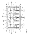
- FIG 7 shows the equivalent circuit network of the particular embodiment of Figure 6 .
- each of the posts is figured as a resonant circuit 79 and the couplings between the posts are figured by double curved arrows 71, 72, 73, 74 and 75.
- the input and output ports are figured by L-C circuits 76, 77 and 78
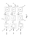
- Figure 8 illustrates a particular embodiment of a device corresponding to the main structure illustrated on figure 6 .
- the device is manufactured in metal, aluminium for example. It comprises a body 81 and a cover, or lid, 82.
- Metallic posts for resonators 641, 651, 661 and 642, 652, 662, and the internal walls 67, are manufactured directly in the body 81 as well as the six cavities 644, 645, 654, 655, 664 and 665, and as the apertures 656, 647 and 667 for couplings.
- Input and output ports, 643, 653 and 663 are of the coaxial type, SMA connectors for example, and are directly connected, wired, to the parallelepipedic posts 641, 651 and 661 by means of screwed antennas 83.
- Resonator elements take the form of metallic posts 641, 642, 651, 652, 661 and 662.
- the coupling between resonators is besides performed by the means of apertures 646, 656, 666, 647 and 667 that separate the six cavities.
- the cover 82 is a plan metallic cover configured so as to be gathered with the body 81, by the means of screws arranged at the periphery of the device for example. Additionally, the cover 82 may also include tuning screws that are provided for filtering function and for power division balance adjustment. These screws are arranged at specific places on the cover, above each resonating post 641, 642, 651, 652, 661 and 662, and above the spaces separating them, making it possible to modify or adjust the behaviour of each resonator and each coupling separately and adjust its characteristics. In a preferred embodiment these screws are assembled on threaded holes 84 machined in the cover 82.
- the device according to the invention may additionally comprise isolator elements 85 to improve electrical return loss.
- these elements are for example directly connected to input and output ports 643, 653 and 663.
- the device according to the invention makes it possible to perform a bandwidth selection and a power division with just one and a same circuit, comprising lumped elements contributing to both filtering and splitting functions. So, it can be advantageously used as the input section circuit of an Input Multiplexer.
- Such a device can be advantageously designed using classical filter circuits synthesis techniques and can comprise tuning elements to adjust precisely its frequency response and the power balance ratio.
- such a device can be designed in such a way that frequency response can be made arbitrarily complex.
- this structure is applicable to realize any "n ways" power divider, where n is an integer higher than 1. Furthermore, this structure is suitable for building power dividing circuits or devices for which the working frequency bandwidth must be accurately defined and for which minimizing the overall mass and size are that while maintaining maximum performances, is a main target.
Landscapes
- Control Of Motors That Do Not Use Commutators (AREA)
Abstract
The invention relates to a power divider and filter device structure that can particularly be used as an input circuit for an Input Multiplexer (IMUX) device used in telecommunication systems.
The device according to the invention comprises one input port and several output ports, and is configured so as to make several cavities in which resonating posts are located, one post per cavity. The cavities communicate some with the others by means of openings. Cavities are arranged in such a way that and input signal incoming the input port propagates through the device by coupling. The cavities and the resonating posts are configured and arranged in such a way that, as it passes through the device, the input signal is, by one and a same operation, filtered and split in as many output signals as the outputs the device comprises, the energy of the input signal being spread out between the outputs.
The device according to the invention comprises one input port and several output ports, and is configured so as to make several cavities in which resonating posts are located, one post per cavity. The cavities communicate some with the others by means of openings. Cavities are arranged in such a way that and input signal incoming the input port propagates through the device by coupling. The cavities and the resonating posts are configured and arranged in such a way that, as it passes through the device, the input signal is, by one and a same operation, filtered and split in as many output signals as the outputs the device comprises, the energy of the input signal being spread out between the outputs.
Description
- The invention relates to the field of microwave passive devices. It particularly relates to microwave multiplexers and power dividers.
- In some telecommunication systems, the received signal contains several communication channels multiplexed in frequency. In order to process each channel separately, receiver equipments generally comprise an Input Multiplexer (IMUX) device. The IMUX device function is to separate each frequency channel included in the input signal and to send each channel to a different output, so the signal corresponding to each of the channels can be processed separately.
Figure 1 shows a typical block diagram of an IMUX device. - Such a microwave device comprises an input channel and several separate output channels each of them consisting in a filter transmitting a signal with a limited bandwidth. Said bandwidth corresponds to that of the communication channel the output channel is supposed to transmit. To this purpose the filter is configured to limit the bandwidth of the input signal to that of the communication channel.
- In order to achieve this function the output channels are generally separated in two groups, to minimize interaction between adjacent channels. Each group covers a part of the whole bandwidth of the input signal and the sum of the bandwidths of the two groups is equal the complete bandwidth of the input signal. In most common embodiments, each of the two groups substantially covers a half of the complete bandwidth.
- For this purpose IMUX generally comprises a splitting input section comprising a filter associated to a power splitter/divider. The input section filter is intended to match the bandwidth of the input signal, while rejecting useless bands. The filtered input signal is then transmitted to the different communication channels. Such a configuration avoids signals out of the useful band to reach the active equipment, which could reduce the system performance dramatically.
- In such an input section, as shown on
figure 1 , the power divider function splits an input signal into two outputs, each one with half the power of the input signal. - Well known microwave structures can be used to achieve this function with minimum power loss due to dissipation and mismatch and with minimum distortion of the input signal. Such a structure generally comprises two separate elements, a filtering element and a power splitting element, connected together by connection means. A drawback of such a configuration is that as the filter element and the splitter element are built and adjusted separately a further adjustment must be done when the two elements are connected together so as to realize the optimal adjustment of the complete structure. This optimal adjustment is important to minimize power loss and distortion of the input signal.
- Another drawback of such a structure is that as it is made with two separate elements performing two different functions, the size of the complete structure mainly depends on the size of each element. Consequently, a reduction of the overall size of the structure is possible only if the size of one or of both elements is possible.
- Other well known microwave structures can be used to achieve this function with minimum power loss due to dissipation and mismatch and with minimum distortion of the input signal. These structures differ from the aforementioned ones in that they overlap the filtering function and the power dividing function. However, in such structures, the components performing each function are still clearly identifiable.
- An example of such a structure is for described in the
US patent 2,823,356 which discloses a device that can be considered as a single device in which the filtering is applied during power division, and not before, like in the aforementioned structures, though it performs the power division and the band selection using different elements for each function (cavity resonators for filtering and a coupler for power division). However, such a structure does have neither the ability of changing the frequency behaviour by tuning adjustments (bandwidth, centre frequency, selectivity, etc..) nor achieving complex responses. - Another example of such a structure is also described in the
US patent 2,735,069 which discloses a device in which power division can be adjusted. However, frequency behaviour of the filtering function is fixed and not adjustable. - One object of the invention is directed to providing an input section structure making it possible to overcome the drawbacks of the known structures used to make the input section of an Input Multiplexer.
- A more general object of the invention is to provide a structure able to combine in one and a same device a filtering and a splitting function. Another object is to provide an integrated signal divider/splitter structure able to produce from an input signal two signals of the same power with a strictly limited bandwidth whatever the bandwidth of the input signal could be. Another object of the invention is to provide an input function that can be controlled for the frequency behaviour as well as for the power balance.
- To this end, the subject of the invention is a power divider and filter in a single device, characterized in that it comprises one input and N outputs, and P coupled resonant elements, said device splitting an input signal into N different output signals with a given equal pre-designed and adjustable frequency bandwidth, the power of the input signal being shared between the output signals in a controllable manner.
- In a preferred embodiment, the device according to the invention comprises a case closed by a cover, said case including an inner space divided into six cavities by internal walls, said cavities communicating with one another by the means of apertures. Each cavity includes a metallic resonating post. One of the posts is configured to receive the input signal, while two other posts are configured to transmit a filtered output signal. The input signal is transmitted from the input to the separate outputs by coupling between the posts. The size and shape of the apertures and the distances between the posts is defined in order to obtain the desired bandwidth for the two output signals as well as to obtain the desired balance of the powers of these output signals.
- In a particular form of the preferred embodiment of the device according to the invention, the post that is configured to receive the input signal as well as the two posts configured to transmit the two output signals have a parallelepipedic shape, while the other posts have a cylindrical shape.
- In another particular form of the preferred embodiment of the device according to the invention, the input post and the two output posts are respectively linked to input or output ports.
- In a preferred embodiment of the device according to the invention, the cover comprise thread holes configured to receive power balance and bandwidth adjustment screws, said holes being arranged on the surface of the cover in order to face the posts or the apertures which separate the different cavities.
- Another subject of the invention is a multiplexer device configured to split a signal received on an input port into several output signals each of them being transmitted to a separate output port, each output signal having a given bandwidth and a power level corresponding to a given part of the input signal power level. According to the invention, as its output ports are gathered in two sets, the multiplexer device comprises a power divider and filter device according to the invention which inputs are connected to the input of the multiplexer device, each of the two output signals produced by the power divider and filter device being transmitted to one of the two sets of output ports.
- The characteristics and advantages of the invention will be better appreciated from the following description, which explains the invention through a particular embodiment taken as a non limiting example and which is based on the appended figures, which represent:
-
figure 1 , a schematic diagram of an input multiplexer commonly used in a telecommunication system, -
figure 2 , an overview of a first example of input device commonly used to feed an IMUX, -
figure 3 , an overview of a second example of input device commonly used to feed an IMUX, -
figure 4 , a schematic diagram illustrating the operating concept of the invention, -
figure 5 , a schematic diagram illustrating the general operating principle of an input section according to the invention, -
figure 6 , a simplified extended view of the main part of the device according to one embodiment of the invention; -
figure 7 , a view of the equivalent circuit network corresponding to the particular embodiment offigure 6 . -
figure 8 , a blow-up overall view of the input device according to the invention. - The proposed input section device according to the invention is an alternate improvement to current input sections. As stated before, current input sections use different elements to realize the two different functions of an input section.
-
Figure 1 illustrates the functional diagram of an input multiplexer, IMUX, commonly used in telecommunication equipments (receivers). Such a device mainly comprises two parts, an input part consisting in theinput section 12 which comprises aninput port 121 and two output ports, 122 and 123, and an output part comprising twoseparate sets - Each set of
output channels input section 12 and N output ports, 151 or 161, each port corresponding to one of the output channels of the IMUX device. The example offigure 1 shows an IMUX device with two sets of output channels each of them comprising N = 4 channels. - Each output channel of an IMUX mainly comprises a
band pass filter 17 the bandwidth of which corresponding to the bandwidth of one the communication channels. Moreover the bandwidths of the filters, Δf1 to Δf8 in the example, are generally configured so as to cover the whole communication bandwidth ΔF. - According to the prior art illustrated by
figure 1 , theinput section 12 mainly comprises an input two separate elements, aband pass filter 13 followed by a power splitter/divider 14. Theband pass filter 13 is configured so as to match the whole communication bandwidth and strongly reject out-of-band signals. Thepower divider 14 generally shares out the input signal received by the input section in output signal, generally of the same power, each signal being sent to one of the two output ports of thesection 12. -
Figure 2 , illustrates a first example of device known of the prior art, achieving theinput section function 12. In this example, the input section has wave guide structure comprising two separate coupleddevices -
Figure 3 , illustrates a second example of device known of the prior art. In this second example, the input section has a planar structure comprising two separate devices in one and a same embodiment. Said structure comprises a power dividermain element 31, with aterminal part 32 corresponding to the twooutput ports main element 31. Themain element 31 has aninitial part 35 where theinput port 36 is connected, this port comprising a band pass filter at its beginning. - It can be noticed that these two structures correspond to two different possible embodiments of an input section structure, each of them having its advantages and its drawbacks. However, as stated before, and as it can be noticed from
figures 3 and4 , both of the structures share the same drawback of achieving the splitting and filtering functions separately, function being implemented after the other. -
Figure 4 shows a schematic diagram illustrating the operating concept of the invention. - The main functional principles of the invention are based on the known methods for microwave filters design. Microwave filters are 2-port devices that show a frequency response according to some electrical requirements. Design methods generally take those requirements and construct an ideal mathematical response (typically a Chebyshev response) that corresponds to them. This ideal mathematical response can be then materialized by an electrical circuit with lumped components, based on resonators and couplers as illustrated on
figure 4 . - The use of known synthesis methods makes it possible to design an equivalent electrical network whose response better fits the mathematical ideal curve. It is thus possible to approximate the desired response by building a microwave structure that has the resonance and coupling characteristics of the ideal equivalent circuit.
- As illustrated, the so designed
circuit 41 comprisesresonators elements resonators -
Other resonators 42, coupled to theport resonators figure 4 , and transmit it to the output circuit illustrated by a resistor RL. The frequency response of the device is given by its topology and depends on the coupling matrix of the equivalent electrical network. - The same concept could be extended to more general networks like the circuit shown in
Figure 5 , which illustrates the behaviour of a general input section with oneinput 51, N outputs 52 and P coupled resonatingelements 53, where both input and output ports can be connected/coupled to one or more resonating elements. - Since the equivalent electrical circuit is defined, an analysis of the physical dimensions that determine the electrical properties of the microwave structure elements corresponding to those of the equivalent electrical circuit can be performed. This analysis can be done using any adequate known method. Such analysis advantageously makes it possible to relate the physical dimensions of the microwave structure elements used to build the desired device to the values of the corresponding elements of the equivalent electrical circuit. The structure so established can moreover be tested in an electromagnetic simulator and optimized the values of the different elements to match at best the desired characteristics.
- Using such methods it is thus possible to build up a device as a circuit comprising lumped elements. This makes it possible to design a device comprising several elements in which interactions M between the
different elements - Moreover the characteristics of the different elements and their arrangement can be determined in order to build up, as a single device, a device comprising two identical filters with a common input, and two separate outputs, each filter delivering a filtered signal on the corresponding output and processing a signal which energy is equal to a half of the energy of the signal received at the common input.
- In must be noted that in such devices different signal paths can be distinguished, those paths sharing a common part near the input of the device. The balance of the power division is thus controlled by modifying the coupling values in the common part, while the shape of the frequency response is controlled by the coupling and resonance values of the whole structure. Thus the achievable frequency response can be made quite complex. It can include transmission nulls for certain frequencies as well as it can reduce signal distortion in the desired frequency band, or even allow breaking the symmetry with respect the central frequency.
-
Figure 6 shows a schematic view of the main structure of the device according to the invention in a particular embodiment given as an example. According to the invention this embodiment corresponds to a device implementing power splitting and frequency filtering in one and a same operation. - The device according to the invention mainly comprises a main
metallic cavity 61 partly divided by two internalmetallic walls 67 in order to form sixcavities metallic posts - In a preferred embodiment,
metallic posts outputs other posts - According to the invention, the dimensions of the different cavities as well as the sizes of the metallic posts are determined, in a known manner, in relation to the frequency and the input power of the signal. As stated before, these determinations can be made using the methods aforementioned. In the other hand the distances between the different posts, as well as the sizes of the apertures between the posts, control the coupling between posts.
- According to the invention too, the
resonant post 651 is connected to the input signal by connection means providing acoaxial input 653. Similarly, lateralresonant posts coaxial connection - Thus, an incoming signal propagates from the input coaxial line to the inner part of the filter through the first resonating
post 651 which transmits it to resonatingpost 652, being the distance between both posts and the width of theaperture 656 the mechanism used to control the bandwidth. Then, the signal transmitted bypost 652 is split up into two parts, each part being transmitted to one of the two resonatingposts apertures posts output resonating posts - Thus, according to the invention, the desired bandwidth of the device is obtained by controlling the distance between the posts located in each of the cavities and the sizes of the
apertures apertures cavities - In such a structure, the metallic posts resonate by themselves, storing and relaxing the electromagnetic energy contained in the communication signal as it flows through the device. The electromagnetic energy is thus propagated between posts directly, using the distance between posts and the widths of the
apertures Cylindrical posts post 651 constitutes the input resonator that introduces the signal inside the device, and whileposts outputs lines figure 6 . -
Figure 7 shows the equivalent circuit network of the particular embodiment ofFigure 6 . On this figure each of the posts is figured as aresonant circuit 79 and the couplings between the posts are figured by doublecurved arrows L-C circuits - The device according to the invention can be manufactured in different ways.
Figure 8 illustrates a particular embodiment of a device corresponding to the main structure illustrated onfigure 6 . - In this particular embodiment the device is manufactured in metal, aluminium for example. It comprises a
body 81 and a cover, or lid, 82. Metallic posts forresonators internal walls 67, are manufactured directly in thebody 81 as well as the sixcavities apertures - Input and output ports, 643, 653 and 663, are of the coaxial type, SMA connectors for example, and are directly connected, wired, to the
parallelepipedic posts antennas 83. - Resonator elements take the form of
metallic posts apertures - According to this embodiment, the
cover 82 is a plan metallic cover configured so as to be gathered with thebody 81, by the means of screws arranged at the periphery of the device for example. Additionally, thecover 82 may also include tuning screws that are provided for filtering function and for power division balance adjustment. These screws are arranged at specific places on the cover, above each resonatingpost holes 84 machined in thecover 82. - As it can be seen on
figure 8 , the device according to the invention may additionally compriseisolator elements 85 to improve electrical return loss. In the embodiment offigure 8 these elements are for example directly connected to input andoutput ports - Thus, the device according to the invention, as afore described makes it possible to perform a bandwidth selection and a power division with just one and a same circuit, comprising lumped elements contributing to both filtering and splitting functions. So, it can be advantageously used as the input section circuit of an Input Multiplexer.
- Such a device can be advantageously designed using classical filter circuits synthesis techniques and can comprise tuning elements to adjust precisely its frequency response and the power balance ratio. In addition, such a device can be designed in such a way that frequency response can be made arbitrarily complex.
- More generally, this structure is applicable to realize any "n ways" power divider, where n is an integer higher than 1. Furthermore, this structure is suitable for building power dividing circuits or devices for which the working frequency bandwidth must be accurately defined and for which minimizing the overall mass and size are that while maintaining maximum performances, is a main target.
Claims (7)
- A power divider and filter in a single device, characterized in that it comprises one input (653) and N outputs (643, 663), and P coupled resonant elements (641, 651, 661, 642, 652, 662), said device splitting an input signal into N different output signals with a given equal pre-designed and adjustable frequency bandwidth, the power of the input signal being shared between the output signals in a controllable manner.
- The device as claimed in claim 1, characterized in that it further comprises a case (81) closed by a cover (82), said case including an inner space divided into six cavities (644, 645, 654, 655, 664 and 665) by internal walls (67), said cavities communicating with one another by the means of apertures (646, 647, 656, 666 and 667), each cavity including a metallic resonating post (641, 642, 651, 652, 661, 662), one post (651) being configured to receive the input signal, while two other posts (641, 661) are configured to transmit a filtered output signal, the input signal being transmitted from the input to the separate outputs by coupling between the posts; the size and shape of the apertures and the distances between the posts being defined in order to obtain the desired bandwidth for the two output signals as well as to obtain the desired balance of the powers of these output signals.
- The device according to claim 2, characterized in that the post (651) configured to receive the input signal as well as the two posts (641, 661) configured to transmit the two output signals have a parallelepipedic shape, while the other posts (642, 652, 662) have a cylindrical shape.
- The device according to claim 2 or 3, characterized in that the input post (651) and the two output posts (641, 661) are respectively linked to input (653) or output (643, 663) ports.
- The device according to any of the preceding claims 2 to 4, characterized in that the cover (82) comprise thread holes (84) configured to receive power balance and bandwidth adjustment screws, said holes being arranged on the surface of the cover in order to face the posts or the apertures which separate the different cavities.
- A multiplexer device configured to split a signal received on an input port (11) into several output signals each of them being transmitted to a separate output port(151, 161), each output signal having a given bandwidth and a power level corresponding to a given part of the input signal power level, characterized in that the output ports of the multiplexer device being gathered in two sets (15, 16), it comprises a power divider and filter device (12) according to any of the previous claims, the input (121) of the power divider and filter device being connected to the input (11) of the multiplexer device, each of the two output signals (122, 123) produced by the power divider and filter device (12) being transmitted to one of the two sets (15, 16) of output ports.
- Any particular realization of the claim 1, independently of the element or technology used to implement the resonant elements, independently of the coupling mechanism implemented, independently of the technique used to connect the input port and the N output ports to the corresponding port resonators, and independently of the mechanisms used to adjust the frequency bandwidth and/or the power division.
Priority Applications (4)
| Application Number | Priority Date | Filing Date | Title |
|---|---|---|---|
| EP09290971A EP2337145A1 (en) | 2009-12-18 | 2009-12-18 | Compact and adjustable power divider and filter device |
| CA2725903A CA2725903A1 (en) | 2009-12-18 | 2010-12-17 | Compact and adjustable power divider and filter device |
| JP2010283196A JP2011130448A (en) | 2009-12-18 | 2010-12-20 | Compact and adjustable power divider and filter device |
| US12/973,202 US20110317714A1 (en) | 2009-12-18 | 2010-12-20 | Compact and adjustable power divider and filter device |
Applications Claiming Priority (1)
| Application Number | Priority Date | Filing Date | Title |
|---|---|---|---|
| EP09290971A EP2337145A1 (en) | 2009-12-18 | 2009-12-18 | Compact and adjustable power divider and filter device |
Publications (1)
| Publication Number | Publication Date |
|---|---|
| EP2337145A1 true EP2337145A1 (en) | 2011-06-22 |
Family
ID=42174140
Family Applications (1)
| Application Number | Title | Priority Date | Filing Date |
|---|---|---|---|
| EP09290971A Withdrawn EP2337145A1 (en) | 2009-12-18 | 2009-12-18 | Compact and adjustable power divider and filter device |
Country Status (4)
| Country | Link |
|---|---|
| US (1) | US20110317714A1 (en) |
| EP (1) | EP2337145A1 (en) |
| JP (1) | JP2011130448A (en) |
| CA (1) | CA2725903A1 (en) |
Cited By (2)
| Publication number | Priority date | Publication date | Assignee | Title |
|---|---|---|---|---|
| CN102683787A (en) * | 2012-04-23 | 2012-09-19 | 安徽科瑞达通信科技有限公司 | Novel cavity low-pass prototype power divider |
| WO2014029182A1 (en) * | 2012-08-21 | 2014-02-27 | 华南理工大学 | Unequal power divider integrated with bandpass filter function |
Families Citing this family (5)
| Publication number | Priority date | Publication date | Assignee | Title |
|---|---|---|---|---|
| CN105846019B (en) * | 2016-06-02 | 2021-05-28 | 京信通信技术(广州)有限公司 | Double-layer cavity common-port combiner |
| CN107658535B (en) * | 2017-09-29 | 2019-12-20 | 中邮科通信技术股份有限公司 | Integrated integration of multisystem closes way platform |
| JP7367209B2 (en) * | 2019-10-15 | 2023-10-23 | 華為技術有限公司 | combiner |
| CN111669148B (en) * | 2020-06-19 | 2023-03-14 | 中国电子科技集团公司第二十六研究所 | Tunable bandpass filter, apparatus and method |
| US20220086966A1 (en) * | 2020-09-14 | 2022-03-17 | Tsinghua University | Microwave transmission method and single-input multiple-output microwave system based on frequency control, and electronic device |
Citations (7)
| Publication number | Priority date | Publication date | Assignee | Title |
|---|---|---|---|---|
| US2735069A (en) | 1956-02-14 | Directional coupler | ||
| US2823356A (en) | 1952-12-11 | 1958-02-11 | Bell Telephone Labor Inc | Frequency selective high frequency power dividing networks |
| GB2020490A (en) * | 1978-01-19 | 1979-11-14 | Marconi Co Ltd | Waveguide junctions |
| DE10320620B3 (en) * | 2003-05-08 | 2004-11-04 | Kathrein-Werke Kg | High crossover |
| WO2005091428A1 (en) * | 2004-03-22 | 2005-09-29 | Filtronic Comtek Oy | Input arrangement for a low-noise amplifier pair |
| WO2008110040A1 (en) * | 2007-03-12 | 2008-09-18 | Comba Telecom System (China) Ltd. | Double frequency combiner |
| EP2073303A1 (en) * | 2007-12-17 | 2009-06-24 | NEC Corporation | Filter having switch function and band pass filter |
Family Cites Families (1)
| Publication number | Priority date | Publication date | Assignee | Title |
|---|---|---|---|---|
| US4602229A (en) * | 1983-12-30 | 1986-07-22 | Motorola, Inc. | Resonant bandpass T filter and power splitter |
-
2009
- 2009-12-18 EP EP09290971A patent/EP2337145A1/en not_active Withdrawn
-
2010
- 2010-12-17 CA CA2725903A patent/CA2725903A1/en not_active Abandoned
- 2010-12-20 JP JP2010283196A patent/JP2011130448A/en active Pending
- 2010-12-20 US US12/973,202 patent/US20110317714A1/en not_active Abandoned
Patent Citations (7)
| Publication number | Priority date | Publication date | Assignee | Title |
|---|---|---|---|---|
| US2735069A (en) | 1956-02-14 | Directional coupler | ||
| US2823356A (en) | 1952-12-11 | 1958-02-11 | Bell Telephone Labor Inc | Frequency selective high frequency power dividing networks |
| GB2020490A (en) * | 1978-01-19 | 1979-11-14 | Marconi Co Ltd | Waveguide junctions |
| DE10320620B3 (en) * | 2003-05-08 | 2004-11-04 | Kathrein-Werke Kg | High crossover |
| WO2005091428A1 (en) * | 2004-03-22 | 2005-09-29 | Filtronic Comtek Oy | Input arrangement for a low-noise amplifier pair |
| WO2008110040A1 (en) * | 2007-03-12 | 2008-09-18 | Comba Telecom System (China) Ltd. | Double frequency combiner |
| EP2073303A1 (en) * | 2007-12-17 | 2009-06-24 | NEC Corporation | Filter having switch function and band pass filter |
Non-Patent Citations (3)
| Title |
|---|
| AVRILLON S ET AL: "DIVIDING AND FILTERING FUNCTION INTEGRATION FOR THE DEVELOPMENT OF A BAND-PASS FILTERING POWER AMPLIFIER", 2002 IEEE MTT-S INTERNATIONAL MICROWAVE SYMPOSIUM DIGEST (CAT. NO.02CH37278) IEEE PISCATAWAY, NJ, USA; [IEEE MTT-S INTERNATIONAL MICROWAVE SYMPOSIUM],, 2 June 2002 (2002-06-02), pages 1173 - 1176, XP001109967, ISBN: 978-0-7803-7239-9 * |
| HIROMITSU UCHIDA ET AL: "Bandpass Directional Couplers with Electromagnetically-Coupled Resonators", MICROWAVE SYMPOSIUM DIGEST, 2006. IEEE MTT-S INTERNATIONAL, IEEE, PI, 1 June 2006 (2006-06-01), pages 1563 - 1566, XP031018781, ISBN: 978-0-7803-9541-1 * |
| SINGH P K ET AL: "Coupled line power divider with compact size and bandpass response", THE INSTITUTION OF ENGINEERING AND TECHNOLOGY. JOURNAL,, vol. 45, no. 17, 13 August 2009 (2009-08-13), pages 892 - 894, XP006033707, ISSN: 1350-911X * |
Cited By (2)
| Publication number | Priority date | Publication date | Assignee | Title |
|---|---|---|---|---|
| CN102683787A (en) * | 2012-04-23 | 2012-09-19 | 安徽科瑞达通信科技有限公司 | Novel cavity low-pass prototype power divider |
| WO2014029182A1 (en) * | 2012-08-21 | 2014-02-27 | 华南理工大学 | Unequal power divider integrated with bandpass filter function |
Also Published As
| Publication number | Publication date |
|---|---|
| US20110317714A1 (en) | 2011-12-29 |
| CA2725903A1 (en) | 2011-06-18 |
| JP2011130448A (en) | 2011-06-30 |
Similar Documents
| Publication | Publication Date | Title |
|---|---|---|
| US20110317714A1 (en) | Compact and adjustable power divider and filter device | |
| EP2332208B1 (en) | A reconfigurable filter apparatus | |
| US10243539B2 (en) | Radio frequency transmit filter with integrated impedance matching network | |
| US6806791B1 (en) | Tunable microwave multiplexer | |
| KR20100104012A (en) | Monoblock dielectric multiplexer for multi-band | |
| CN110444844B (en) | Single-channel and multi-channel reconfigurable filter circuit | |
| US7764146B2 (en) | Cavity microwave filter assembly with lossy networks | |
| CA2526766C (en) | Generalized multiplexing network | |
| US9391585B2 (en) | Compact multi-port router device | |
| Tu et al. | Design of microwave microstrip multiband diplexers for system in package | |
| US20110187477A1 (en) | Apparatus for filtering an input signal | |
| CN112038740A (en) | Miniaturized multiplexer | |
| CN205621824U (en) | Five multiplexers of low pass - band -pass based on novel frequency separation structure | |
| CA2795528C (en) | Multi-band filter | |
| WO2017042560A1 (en) | A microwave switched multiplexer and a mobile telecommunications device including such a multiplexer | |
| CN107196027B (en) | A kind of eight double-channel duplex devices of miniaturization | |
| CN212648441U (en) | Miniaturized multiplexer | |
| CN113228408A (en) | Medium duplexer | |
| Ezzeddine et al. | Design of a compact dual-band diplexer with dual-mode cavities | |
| US20100090784A1 (en) | Programmable Tunable Filter Waveguide | |
| WO2023159482A1 (en) | A communication device | |
| CN115473019B (en) | Filter power divider with reconfigurable arbitrary channel number and radio frequency front end | |
| Resnati et al. | Combining 2G and 3G (4G) BTS outputs sharing the same frequency band | |
| WO2017203216A1 (en) | Multi-band filter apparatus and method of use thereof | |
| Doan et al. | Tri-band bandpass filter using dual-mode resonators |
Legal Events
| Date | Code | Title | Description |
|---|---|---|---|
| PUAI | Public reference made under article 153(3) epc to a published international application that has entered the european phase |
Free format text: ORIGINAL CODE: 0009012 |
|
| AK | Designated contracting states |
Kind code of ref document: A1 Designated state(s): AT BE BG CH CY CZ DE DK EE ES FI FR GB GR HR HU IE IS IT LI LT LU LV MC MK MT NL NO PL PT RO SE SI SK SM TR |
|
| AX | Request for extension of the european patent |
Extension state: AL BA RS |
|
| 17P | Request for examination filed |
Effective date: 20111222 |
|
| 17Q | First examination report despatched |
Effective date: 20171023 |
|
| STAA | Information on the status of an ep patent application or granted ep patent |
Free format text: STATUS: THE APPLICATION IS DEEMED TO BE WITHDRAWN |
|
| 18D | Application deemed to be withdrawn |
Effective date: 20180303 |