EP2284594B1 - Display including waveguide, micro-prisms and micro-mechanical light modulators - Google Patents
Display including waveguide, micro-prisms and micro-mechanical light modulators Download PDFInfo
- Publication number
- EP2284594B1 EP2284594B1 EP10008145.4A EP10008145A EP2284594B1 EP 2284594 B1 EP2284594 B1 EP 2284594B1 EP 10008145 A EP10008145 A EP 10008145A EP 2284594 B1 EP2284594 B1 EP 2284594B1
- Authority
- EP
- European Patent Office
- Prior art keywords
- light
- micro
- prisms
- display according
- tilting
- Prior art date
- Legal status (The legal status is an assumption and is not a legal conclusion. Google has not performed a legal analysis and makes no representation as to the accuracy of the status listed.)
- Not-in-force
Links
Images


Classifications
-
- G—PHYSICS
- G02—OPTICS
- G02B—OPTICAL ELEMENTS, SYSTEMS OR APPARATUS
- G02B5/00—Optical elements other than lenses
- G02B5/04—Prisms
- G02B5/045—Prism arrays
-
- G—PHYSICS
- G02—OPTICS
- G02B—OPTICAL ELEMENTS, SYSTEMS OR APPARATUS
- G02B26/00—Optical devices or arrangements for the control of light using movable or deformable optical elements
- G02B26/08—Optical devices or arrangements for the control of light using movable or deformable optical elements for controlling the direction of light
- G02B26/0816—Optical devices or arrangements for the control of light using movable or deformable optical elements for controlling the direction of light by means of one or more reflecting elements
- G02B26/0833—Optical devices or arrangements for the control of light using movable or deformable optical elements for controlling the direction of light by means of one or more reflecting elements the reflecting element being a micromechanical device, e.g. a MEMS mirror, DMD
- G02B26/0841—Optical devices or arrangements for the control of light using movable or deformable optical elements for controlling the direction of light by means of one or more reflecting elements the reflecting element being a micromechanical device, e.g. a MEMS mirror, DMD the reflecting element being moved or deformed by electrostatic means
-
- G—PHYSICS
- G02—OPTICS
- G02B—OPTICAL ELEMENTS, SYSTEMS OR APPARATUS
- G02B6/00—Light guides; Structural details of arrangements comprising light guides and other optical elements, e.g. couplings
- G02B6/0001—Light guides; Structural details of arrangements comprising light guides and other optical elements, e.g. couplings specially adapted for lighting devices or systems
- G02B6/0011—Light guides; Structural details of arrangements comprising light guides and other optical elements, e.g. couplings specially adapted for lighting devices or systems the light guides being planar or of plate-like form
- G02B6/0033—Means for improving the coupling-out of light from the light guide
- G02B6/0035—Means for improving the coupling-out of light from the light guide provided on the surface of the light guide or in the bulk of it
- G02B6/0036—2-D arrangement of prisms, protrusions, indentations or roughened surfaces
-
- G—PHYSICS
- G02—OPTICS
- G02B—OPTICAL ELEMENTS, SYSTEMS OR APPARATUS
- G02B6/00—Light guides; Structural details of arrangements comprising light guides and other optical elements, e.g. couplings
- G02B6/0001—Light guides; Structural details of arrangements comprising light guides and other optical elements, e.g. couplings specially adapted for lighting devices or systems
- G02B6/0011—Light guides; Structural details of arrangements comprising light guides and other optical elements, e.g. couplings specially adapted for lighting devices or systems the light guides being planar or of plate-like form
- G02B6/0033—Means for improving the coupling-out of light from the light guide
- G02B6/0035—Means for improving the coupling-out of light from the light guide provided on the surface of the light guide or in the bulk of it
- G02B6/0038—Linear indentations or grooves, e.g. arc-shaped grooves or meandering grooves, extending over the full length or width of the light guide
-
- G—PHYSICS
- G02—OPTICS
- G02B—OPTICAL ELEMENTS, SYSTEMS OR APPARATUS
- G02B6/00—Light guides; Structural details of arrangements comprising light guides and other optical elements, e.g. couplings
- G02B6/0001—Light guides; Structural details of arrangements comprising light guides and other optical elements, e.g. couplings specially adapted for lighting devices or systems
- G02B6/0011—Light guides; Structural details of arrangements comprising light guides and other optical elements, e.g. couplings specially adapted for lighting devices or systems the light guides being planar or of plate-like form
- G02B6/0033—Means for improving the coupling-out of light from the light guide
- G02B6/0035—Means for improving the coupling-out of light from the light guide provided on the surface of the light guide or in the bulk of it
- G02B6/0045—Means for improving the coupling-out of light from the light guide provided on the surface of the light guide or in the bulk of it by shaping at least a portion of the light guide
- G02B6/0046—Tapered light guide, e.g. wedge-shaped light guide
-
- G—PHYSICS
- G09—EDUCATION; CRYPTOGRAPHY; DISPLAY; ADVERTISING; SEALS
- G09G—ARRANGEMENTS OR CIRCUITS FOR CONTROL OF INDICATING DEVICES USING STATIC MEANS TO PRESENT VARIABLE INFORMATION
- G09G3/00—Control arrangements or circuits, of interest only in connection with visual indicators other than cathode-ray tubes
- G09G3/20—Control arrangements or circuits, of interest only in connection with visual indicators other than cathode-ray tubes for presentation of an assembly of a number of characters, e.g. a page, by composing the assembly by combination of individual elements arranged in a matrix no fixed position being assigned to or needed to be assigned to the individual characters or partial characters
- G09G3/34—Control arrangements or circuits, of interest only in connection with visual indicators other than cathode-ray tubes for presentation of an assembly of a number of characters, e.g. a page, by composing the assembly by combination of individual elements arranged in a matrix no fixed position being assigned to or needed to be assigned to the individual characters or partial characters by control of light from an independent source
- G09G3/3433—Control arrangements or circuits, of interest only in connection with visual indicators other than cathode-ray tubes for presentation of an assembly of a number of characters, e.g. a page, by composing the assembly by combination of individual elements arranged in a matrix no fixed position being assigned to or needed to be assigned to the individual characters or partial characters by control of light from an independent source using light modulating elements actuated by an electric field and being other than liquid crystal devices and electrochromic devices
- G09G3/3473—Control arrangements or circuits, of interest only in connection with visual indicators other than cathode-ray tubes for presentation of an assembly of a number of characters, e.g. a page, by composing the assembly by combination of individual elements arranged in a matrix no fixed position being assigned to or needed to be assigned to the individual characters or partial characters by control of light from an independent source using light modulating elements actuated by an electric field and being other than liquid crystal devices and electrochromic devices based on light coupled out of a light guide, e.g. due to scattering, by contracting the light guide with external means
Definitions
- the present invention relates generally to displays. More particularly the invention concerns displays comprising an optical waveguide, a light source and a plurality of electromechanical picture elements.
- Prior art liquid crystal displays typically comprise a backlight assembly for illumination, light polarizers, color and neutral density filters, and an active matrix liquid crystal layer with thin-film-transistor backplanes.
- the overall light efficiency of a typical prior art liquid crystal display (LCD) is below 10% mainly due to the fact that light from the backlight assembly has to pass several layers of polarizers, color and neutral density filters.
- a further problem with LCDs is the slow response time of the liquid crystal resulting in objectionable visible motion artifacts when displaying motion images.
- micro-mechanical flat panel displays based on an optical waveguide were proposed as a viable alternate to LCDs. These displays typically consist of a planar waveguide with parallel surfaces on which a matrix of electrically driven micro-mechanical picture elements is constructed. Light from a light source is introduced to the waveguide from one or more sides of the waveguide and is confined within the waveguide by total internal reflections. Light is extracted from the planar surface of the waveguide by coupling to evanescent waves or by deforming the surface of the planar waveguide to produce an image.
- There is an inherent optical crosstalk problem when picture elements are simultaneously activated to display an image. The state of one picture element changes the brightness of other picture elements.
- One solution to the optical crosstalk problem is to activate the picture elements sequentially.
- US 6,470,115 discloses an optical switching element for realization of an image display.
- the optical switching element comprises a light guide and a light extraction unit mounted on to a thin film.
- the light extraction unit extracts light from the light guide by coupling to the evanescent waves.
- US 2007/0279727 discloses a display which includes an array of light modulators that define a display plane, a light guide and front- and rear-facing reflective surfaces.
- the light guide includes a plurality of geometric light redirectors, and at least 50% of the light guide's rear surface is parallel to the display plane.
- the rear-facing reflective surface is parallel to the display plane and includes a plurality of apertures.
- JP 2006108033 discloses a plurality of surface light emitting units arranged in parallel with one another.
- Each surface light emitting unit U2 has a plate-like light guide body 3 having a refractive index ng.
- a light leakage modulator 8 on the rear side 34 of the light guide body is formed with a composite layer 80 having first and second refraction index regions 81, 82 with refraction indexes n1, n2 (ng>n1, n2>n1), and a third refraction index layer 83 with a refraction index n3 (n3>n1).
- each of plurality of prism columns 9 formed on the surface of the light leakage modulator 8 the inclination of a prism face 91 on the side closer to a primary light source 1 is 80-105 degrease with respect to the light emission surface 33 of the light guide body, and the inclination of prism face 92 on the side further away from the primary light source is 35-55 degrease with respect to the emission surface 33 of the light guide body.
- a display that effectively overcomes the optical crosstalk problem typically found in prior art optical waveguide-based displays.
- this object is achieved by providing a display that comprises a light source and an optical waveguide.
- the optical waveguide distributes light to a plurality of light exits. At each light exit a picture element modulates light by selectively directing the light to the viewer or to a light absorber.
- Another object of the invention is to provide a high contrast display of the character that operates at high levels of ambient light.
- Embodiments of the invention achieve this object by providing a display wherein the majority of the viewing surface is coated with a light-absorbing coating.
- Another object of the invention is to provide a display that can compete with LCD's in light efficiency, picture quality and cost. Increased light efficiency is achieved by providing a display in which light travels most of the light path by total internal reflections and light is modulated by requiring fewer reflections from highly reflective micro-mirrors. Improved picture quality is achieved by providing fast and efficient light modulators.
- display 20 here includes a generally rectangular shaped optical waveguide 21 that is substantially wedge-shaped cross section.
- Waveguide 21 is preferably constructed from acrylic or other optically transparent material, having a refractive index n1 with a value between approximately 1.45 and approximately 1.6 and comprises parallel first and second end surfaces 26 and 27 that are joined by parallel side surfaces 28 and 29 (see Figure 1 ).
- Waveguide 21 also includes a major upper surface 30 and a lower surface 31 converging with upper surface 30.
- the lower surface 31 as generally shown in Figure 1 is a flat surface and forming an angle 22 ( Figure 2 ) with a value between approximately 0.1 degrees to approximately 2.0 degrees with the upper surface 30. Also the lower surface 31 may be a curved surface forming varying angles with the upper surface 30 of the waveguide 21 or include a plurality of stepwise facets for controlling the display light uniformity.
- a plurality of substantially equally spaced-apart micro-prisms 32 are constructed at upper surface 30 and, as generally shown in Figure 1 , extend between side surfaces 28 and 29. Micro-prisms 32 may be molded or constructed using lithography from a UV curing polymer having a refractive index n2 with a value between approximately 1.45 and approximately 1.6.
- LED light sources 25 are installed proximate the wide edge 26 of the waveguide 21 and a plurality of tilting micro-mirrors 33 are constructed between micro-prisms 32.
- a plurality of tilting micro-mirrors 33 are constructed between micro-prisms 32.
- one column of the tilting micro-mirrors is designated as 33a, 33b, and 33c.
- Figure 1 also illustrates a section of a cover assembly 34. More detailed construction of the cover assembly 34 is illustrated in Figure 3 .
- the first layer is a light reflecting layer 35 constructed from metal or multilayer dielectric materials on the upper surface 30 of the waveguide 21.
- the light reflecting layer 35 is patterned to form plurality of light reflecting regions 36 and light transmitting regions 37.
- the second optical layer is a light transmitting layer 39 formed from a fluoropolymer or other substantially transparent material having a refractive index n3 with a value between approximately 1.3 and approximately 1.4.
- the light transmitting layer 39 is formed only in the light transmitting regions 37 as shown in Figure 3 on the upper surface 30 of the waveguide 21.
- the light transmitting layer 39 may be a continuous layer formed between the light reflecting layer 35 and upper surface 30 of the waveguide 21.
- the third optical layer is a light absorbing layer 40 formed on light reflecting layer 35 and is patterned to partially cover light reflecting layer 35. A black oxide layer may be formed on upper surface of light reflecting layer 35 instead of light absorbing layer 40.
- micro-prisms 32 Each micro-prism 32 comprises a light input facet 41 which is optically coupled to the upper surface 30 of waveguide 21 via light transmitting layer 39 and a light exit facet 42 which is inclined with respect to the upper surface 30 of waveguide 21 and forms an angle 23 with a value between approximately 45 degrees to approximately 65 degrees.
- a reflective mirror film is deposited on the third facet 43 of micro-prisms 32 to form a light reflecting facet 47, which is also inclined with respect to the upper surface 30 of waveguide 21 and forms an angle 24 with a value between approximately 30 degrees to approximately 50 degrees.
- FIG. 3 also illustrates one of the tilting micro-mirrors 33b which typifies the construction of each of the micro-mirrors of the present form of the invention.
- Micro-mirror 33b comprises a thin aluminum alloy elastic film that is affixed to the upper portion of the light exit facet 42 of micro-prism 32 and it tilts in two directions at about axis 50 that is substantially parallel to the upper surface 30 of the waveguide 21.
- Cover assembly 34 which is affixed to the upper facets of micro-prisms 32.
- Cover assembly 34 comprises a substrate 44 made of glass or other substantially transparent material.
- a light absorbing layer 51 constructed on the lower surface 46 of substrate 44 from conductive light absorbing film or a multilayer film that includes a conductor layer.
- the light absorbing layer 51 is patterned to form a plurality of light absorbing regions 49 located directly above micro-mirrors 33 and display light exit regions 48.
- the cover assembly 34 further includes a light shaping diffuser 52 formed on the upper surface 45 of substrate 44.
- a black oxide layer may be formed on upper surface of micro-mirrors 33 and patterned light absorbing layer 51 may be replaced with a transparent conductor. This will remove the requirement of the alignment of patterned light absorbing layer 51 with the micro-mirrors 33.
- the tilting micro-mirrors 33 operate by electrostatic attraction force.
- the conductive light reflecting layer 35 and conductive light absorbing layer 51 act as fixed electrodes for the tilting micro-mirrors 33.
- the micro-mirror tilts down by electrostatic attraction force.
- a suitable voltage is applied between the conductive light absorbing layer 51 and a micro-mirror 33, the micro-mirror tilts up by electrostatic attraction force.
- a small gap 58 ( Figure 2 ) is required between the edge of the micro-mirrors and the landing surfaces. This may be realized by constructing small spacers on landing surfaces or extending small portions of micro-mirrors along the edge so the entire edge of the micro-mirrors do not touch the landing surfaces.
- light rays 55 entering from the wide edge 26 of the waveguide 21 reflect from the upper surface 30 and the lower surface 31 by total internal reflections and change angles towards normal with respect to the upper surface 30.
- Light rays 55 exit the waveguide 21 from the light transmitting regions 37 ( Figure 3 ) when the incident angle is less than the critical angle 38 defined by the refractive index n1 of the waveguide 21 and refractive index n3 of light transmitting layer 39.
- Light rays passing through the light transmitting layer 39 enter the micro-prisms 32 from the light input facet 41 and change the angle defined by the refractive index n2 of the micro-prisms.
- Light rays exit the micro-prisms from the light exit facets 42.
- a tilting micro-mirror is in the up position, such as micro mirror 33b ( Figure 2 )
- most light rays exiting from light exit facet 42 of micro-prisms 32 reflect from the lower surface of the micro-mirrors and are directed to the viewer by reflecting from light reflecting facets 47.
- a micro-mirror is tilted down, such as micro-mirrors 33a and 33c, most light rays exiting from light exit facet 42 of micro-prisms 32 reflect from the lower surface of the micro-mirrors and are absorbed in the light absorbing layer 40.
- the display 20 limits the minimum angle that light rays can exit from the light exit facets 42 of the micro-prisms 32 with respect to the upper surface 30 of the waveguide 21.
- the minimum angle is defined by the refractive indexes n1, n2, n3 and angle 23.
- FIG. 4 of the drawings a cross-sectional view of another embodiment of display of the present invention is there shown and generally designated by the numeral 70.
- This latest embodiment is similar in some respect to the embodiment shown in Figures 1 and 2 of the drawings and like numbers are used in Figure 4 to identify like components.
- the display 70 is a full color display wherein each picture element comprises of Red, Green and Blue sub-pixels and includes dichoric filters for separating RGB colors from a white light source or from RGB light sources that are mixed in the waveguide 21.
- the display 70 includes optical waveguide 21 and LED light sources 25 that are installed proximate the wide edge 26 of the waveguide 21.
- Display 70 also includes a substrate 72 constructed from a substantially transparent material such as glass having a refractive index n4 with a value between approximately 1.45 and approximately 1.6.
- the lower surface 74 of substrate 72 is optically coupled to the upper surface 30 of waveguide 21 via an optical layer 71 formed from a substantially transparent material having a refractive index n3 with a value between approximately 1.3 and approximately 1.4.
- a plurality of equally spaced-apart micro-prisms 32 are constructed at upper surface 73 of substrate 72 and tilting micro-mirrors 33 are constructed between micro-prisms 32.
- cover assembly 34 is affixed to the upper facets of micro-prisms 32.
- the first optical layer is a dichroic filter 75 formed on the upper surface 73 of the substrate 72.
- the second optical layer is a light reflecting layer 35 constructed from metal on the dichroic filter 75.
- the light reflecting layer 35 is patterned to form plurality of light reflecting regions 36 and light transmitting regions 37.
- the third optical layer is a light absorbing layer 40 formed on light reflecting layer 35 and is patterned to partially cover light reflecting layer 35.
- micro-prisms 32 are also illustrated in Figure 5.
- Each micro-prism 32 comprises a light input facet 41, which is optically coupled to the upper surface 30 of waveguide 21 via dichroic filter 75, substrate 72 and optical layer 71.
- Each micro-prism 32 also includes a light exit facet 42 and a mirror film is deposited on the third facet 43 of micro-prisms 32 to form light reflecting facets 47.
- Figure 5 also illustrates one of micro-mirrors 33 and cover assembly 34 that was described before in Figure 3 .
- light rays 55 entering from the wide edge 26 of the waveguide 21 reflect from the upper surface 30 and the lower surface 31 by total internal reflections and change angles towards normal with respect to the upper surface 30.
- Light rays 55 exit the waveguide 21 from the upper surface 30 and enter substrate 72 through the light transmitting layer 71 when the incident angle is less than critical angle 38 ( Figure 5 ) defined by the refractive index n1 of the waveguide 21 and refractive index n3 of light transmitting layer 71.
- Dichroic filters selectively pass RGB colors in the light transmitting regions 37 into the micro-prisms 32. And light exits micro-prisms 32 from the light exit facets 42. As before depending on the positions of the tilting micro-mirrors, light rays are absorbed, or directed to the viewer.
- FIG. 80 another embodiment of display of the present invention is there shown and generally designated by the numeral 80.
- the display 80 includes optical waveguide 21, light sources 25 that are installed proximate the wide edge 26 of the waveguide 21 and micro-prisms 32 are constructed at upper surface 30 and, as generally shown in Figure 6 , extend between side surfaces 28 and 29 of the waveguide 21.
- the display 80 further includes a plurality of tilting micro-shutters 81 that are constructed between micro-prisms 32.
- one column of the tilting micro-shutters is designated as 81a, 81b, and 81c.
- Figure 6 also illustrates a section of a cover assembly 84. More detailed construction of the cover assembly 84 is illustrated in Figure 8 .
- the first layer is a light reflecting layer 35 constructed from metal or multilayer dielectric materials on the upper surface 30 of the waveguide 21.
- the light reflecting layer 35 is patterned to form plurality of light reflecting regions 36 and light transmitting regions 37.
- the second optical layer is a light transmitting layer 39 formed from a fluoropolymer or other substantially transparent material having a refractive index n3 with a value between approximately 1.3 and approximately 1.4.
- the light transmitting layer 39 is formed only in the light transmitting regions 37 as shown in Figure 8 on the upper surface 30 of the waveguide 21.
- the light transmitting layer 39 may be a continuous layer formed between the light reflecting layer 35 and upper surface 30 of the waveguide 21.
- the third optical layer is a light absorbing layer 82 formed from a dielectric material on light reflecting layer 35 and is patterned to partially cover light reflecting layer 35.
- a black oxide layer may be formed on upper surface of light reflecting layer 35 instead of light absorbing layer 82.
- the light absorbing layer 82 may be replaced with a light absorbing film and placed below the lower surface 31 of the waveguide 21.
- micro-prisms 32 Each micro-prism 32 comprises a light input facet 41 which is optically coupled to the upper surface 30 of waveguide 21 via light transmitting layer 39 and a light exit facet 42 which is inclined with respect to the upper surface 30 of waveguide 21 and forms an angle 23 with a value between approximately 45 degrees to approximately 65 degrees.
- Micro-prisms 32 further include a facet 43 which is inclined opposite to the light exit facet 42 and an upper facet 47 which is generally parallel to the light input facet 41.
- FIG 8 also illustrates one of the tilting micro-shutters 81b which typifies the construction of each of the micro-shutters of the present form of the invention.
- Micro-shutter 81b comprises a thin aluminum alloy elastic film that is affixed to the upper facet 47 of micro-prism 32b and it tilts in two directions at about axis 85 that is substantially parallel to the upper surface 30 of the waveguide 21.
- a black oxide layer or a black polymer film may be formed on surfaces of micro-shutters 81.
- FIG 8 Further illustrated in Figure 8 is a cover assembly 84 which is affixed to the upper surface 30 of waveguide 21 with spacers 83 (see Figure 7 ).
- the construction of the cover assembly 84 is similar to the cover assembly 34 that was described above.
- the tilting micro-shutters 81 operate by electrostatic attraction force.
- the conductive light reflecting layer 35 and conductive light absorbing layer 51 act as fixed electrodes for the tilting micro-shutters 81.
- the micro-shutter tilts down by electrostatic attraction force.
- a suitable voltage is applied between the conductive light absorbing layer 51 and a micro-shutter 81, the micro-shutter tilts up by electrostatic attraction force.
- a small gap is required between the edge of the micro-shutters and the landing surfaces. This may be realized by constructing small spacers from a low friction material on landing surfaces or extending small portions of micro-shutters along the edge so the entire edge of the micro-shutters do not touch the landing surfaces. Additionally the black polymer coatings on the micro-shutters may be formed from a non stick material.
- light rays 55 entering from the wide edge 26 of the waveguide 21 reflect from the upper surface 30 and the lower surface 31 by total internal reflections and change angles towards normal with respect to the upper surface 30.
- Light rays 55 exit the waveguide 21 from the light transmitting regions 37 ( Figure 8 ) when the incident angle is less than the critical angle 38 defined by the refractive index n1 of the waveguide 21 and refractive index n3 of light transmitting layer 39.
- Light rays passing through the light transmitting layer 39 enter the micro-prisms 32 from the light input facet 41 and change the angle defined by the refractive index n2 of the micro-prisms.
- Light rays exit the micro-prisms from the light exit facets 42.
- micro-shutter 81b When a tilting micro-shutter is in the up position, such as micro-shutter 81b ( Figure 7 ), most light rays exiting from light exit facet 42 of micro-prisms 32 are absorbed in light absorber coatings of micro-shutters 81. Any light reflected from the lower surface of the micro-shutters 81 will be absorbed in the light absorbing layer 40.
- micro-shutters 81a and 81c When a micro-shutter is tilted down, such as micro-shutters 81a and 81c, most light rays exiting from light exit facet 42 of micro-prisms 32 exit the display 80 from display light exit regions 48 and are directed to the viewer.
- each picture element of the display panel may include several tilting light modulators. Reducing the size of individual light modulators helps to reduce the required electrostatic actuation voltages.
- each picture element may be grouped to modulate different levels of light when suitable voltage is applied between the fixed electrodes and a selected group of light modulators. This reduces the display addressing constraints.
- each picture element may include 7 light modulators grouped in quantities of 1, 2 and 4 and selectively addressed to modulate 8 levels of light. Additionally, temporal artifacts inherent in pulse-width-modulation displays are reduced.
- antireflection coatings may be applied to surfaces where light transitions between two different materials.
- Dichroic layers that comprise a low pass filter for the Blue color and a high pass filter for the Red color may be formed to overlap in the light reflecting regions 36.
- micro-prisms may be split to lower and upper sections and micro-mirrors may be formed on a flat surface after forming the lower sections of micro-prisms.
Landscapes
- Physics & Mathematics (AREA)
- General Physics & Mathematics (AREA)
- Optics & Photonics (AREA)
- Engineering & Computer Science (AREA)
- Nonlinear Science (AREA)
- Computer Hardware Design (AREA)
- Theoretical Computer Science (AREA)
- Mechanical Light Control Or Optical Switches (AREA)
- Mathematical Physics (AREA)
- Chemical & Material Sciences (AREA)
- Crystallography & Structural Chemistry (AREA)
- Micromachines (AREA)
Description
- The present invention relates generally to displays. More particularly the invention concerns displays comprising an optical waveguide, a light source and a plurality of electromechanical picture elements.
- Currently liquid crystal displays dominate the flat panel display market. Prior art liquid crystal displays typically comprise a backlight assembly for illumination, light polarizers, color and neutral density filters, and an active matrix liquid crystal layer with thin-film-transistor backplanes. The overall light efficiency of a typical prior art liquid crystal display (LCD) is below 10% mainly due to the fact that light from the backlight assembly has to pass several layers of polarizers, color and neutral density filters. A further problem with LCDs is the slow response time of the liquid crystal resulting in objectionable visible motion artifacts when displaying motion images.
- Recently, micro-mechanical flat panel displays based on an optical waveguide were proposed as a viable alternate to LCDs. These displays typically consist of a planar waveguide with parallel surfaces on which a matrix of electrically driven micro-mechanical picture elements is constructed. Light from a light source is introduced to the waveguide from one or more sides of the waveguide and is confined within the waveguide by total internal reflections. Light is extracted from the planar surface of the waveguide by coupling to evanescent waves or by deforming the surface of the planar waveguide to produce an image. There is an inherent optical crosstalk problem when picture elements are simultaneously activated to display an image. The state of one picture element changes the brightness of other picture elements. One solution to the optical crosstalk problem is to activate the picture elements sequentially. This requires very fast micro-mechanical actuators and results in very low light efficiency. Displaying color or grey scale images is generally not practical. Another common problem concerns the use of mirror surfaces to redirect light to the viewer. The same mirror surface reflects the ambient light back to the viewer thereby significantly reducing the contrast at high levels of ambient light.
-
US 6,470,115 discloses an optical switching element for realization of an image display. The optical switching element comprises a light guide and a light extraction unit mounted on to a thin film. The light extraction unit extracts light from the light guide by coupling to the evanescent waves. -
US 2007/0279727 discloses a display which includes an array of light modulators that define a display plane, a light guide and front- and rear-facing reflective surfaces. The light guide includes a plurality of geometric light redirectors, and at least 50% of the light guide's rear surface is parallel to the display plane. The rear-facing reflective surface is parallel to the display plane and includes a plurality of apertures. -
JP 2006108033 rear side 34 of the light guide body is formed with acomposite layer 80 having first and secondrefraction index regions refraction index layer 83 with a refraction index n3 (n3>n1). In each of plurality of prism columns 9 formed on the surface of the light leakage modulator 8, the inclination of a prism face 91 on the side closer to a primary light source 1 is 80-105 degrease with respect to thelight emission surface 33 of the light guide body, and the inclination of prism face 92 on the side further away from the primary light source is 35-55 degrease with respect to theemission surface 33 of the light guide body. - It is an object of the present invention as defined in the appended claims to provide a display that effectively overcomes the optical crosstalk problem typically found in prior art optical waveguide-based displays. In one form of the invention this object is achieved by providing a display that comprises a light source and an optical waveguide. The optical waveguide distributes light to a plurality of light exits. At each light exit a picture element modulates light by selectively directing the light to the viewer or to a light absorber.
- Another object of the invention is to provide a high contrast display of the character that operates at high levels of ambient light. Embodiments of the invention achieve this object by providing a display wherein the majority of the viewing surface is coated with a light-absorbing coating.
- Another object of the invention is to provide a display that can compete with LCD's in light efficiency, picture quality and cost. Increased light efficiency is achieved by providing a display in which light travels most of the light path by total internal reflections and light is modulated by requiring fewer reflections from highly reflective micro-mirrors. Improved picture quality is achieved by providing fast and efficient light modulators.
- The foregoing as well as other objects of the invention will be achieved by the novel display illustrated in the accompanying drawings and described in the specification that follows.
-
-
Figure 1 is a generally perspective view of the display of the present invention. -
Figure 2 is a cross-sectional view taken along lines 2-2 ofFigure 1 . -
Figure 3 is an enlarged view of the area designated as 3-3 inFigure 2 . -
Figure 4 is a generally cross-sectional view of an alternate form of display of the invention. -
Figure 5 is an enlarged view of the area designated as 5-5 inFigure 4 . -
Figure 6 is a generally perspective view of an alternate form of the display of the present invention. -
Figure 7 is a cross-sectional view taken along lines 6-6 ofFigure 6 . -
Figure 8 is an enlarged view of the area designated as 8-8 inFigure 7 . - Referring to the drawings and particularly to
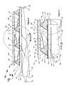
Figures 1 and2 , one form of the display of the invention is shown there and generally designated by thenumeral 20. As best seen inFigure 1 ,display 20 here includes a generally rectangular shapedoptical waveguide 21 that is substantially wedge-shaped cross section. Waveguide 21 is preferably constructed from acrylic or other optically transparent material, having a refractive index n1 with a value between approximately 1.45 and approximately 1.6 and comprises parallel first andsecond end surfaces parallel side surfaces 28 and 29 (seeFigure 1 ). Waveguide 21 also includes a majorupper surface 30 and alower surface 31 converging withupper surface 30. Thelower surface 31 as generally shown inFigure 1 is a flat surface and forming an angle 22 (Figure 2 ) with a value between approximately 0.1 degrees to approximately 2.0 degrees with theupper surface 30. Also thelower surface 31 may be a curved surface forming varying angles with theupper surface 30 of thewaveguide 21 or include a plurality of stepwise facets for controlling the display light uniformity. A plurality of substantially equally spaced-apart micro-prisms 32 are constructed atupper surface 30 and, as generally shown inFigure 1 , extend betweenside surfaces Micro-prisms 32 may be molded or constructed using lithography from a UV curing polymer having a refractive index n2 with a value between approximately 1.45 and approximately 1.6.LED light sources 25 are installed proximate thewide edge 26 of thewaveguide 21 and a plurality of tilting micro-mirrors 33 are constructed between micro-prisms 32. InFigure 2 , one column of the tilting micro-mirrors is designated as 33a, 33b, and 33c.Figure 1 also illustrates a section of acover assembly 34. More detailed construction of thecover assembly 34 is illustrated inFigure 3 . - Now referring to
Figure 3 of the drawings where more details of multilayer optical coatings are shown. The first layer is alight reflecting layer 35 constructed from metal or multilayer dielectric materials on theupper surface 30 of thewaveguide 21. Thelight reflecting layer 35 is patterned to form plurality oflight reflecting regions 36 andlight transmitting regions 37. The second optical layer is alight transmitting layer 39 formed from a fluoropolymer or other substantially transparent material having a refractive index n3 with a value between approximately 1.3 and approximately 1.4. Thelight transmitting layer 39 is formed only in thelight transmitting regions 37 as shown inFigure 3 on theupper surface 30 of thewaveguide 21. Also thelight transmitting layer 39 may be a continuous layer formed between thelight reflecting layer 35 andupper surface 30 of thewaveguide 21. The third optical layer is a light absorbinglayer 40 formed onlight reflecting layer 35 and is patterned to partially coverlight reflecting layer 35. A black oxide layer may be formed on upper surface oflight reflecting layer 35 instead of light absorbinglayer 40. - Further illustrated in
Figure 3 are micro-prisms 32. Each micro-prism 32 comprises alight input facet 41 which is optically coupled to theupper surface 30 ofwaveguide 21 vialight transmitting layer 39 and alight exit facet 42 which is inclined with respect to theupper surface 30 ofwaveguide 21 and forms anangle 23 with a value between approximately 45 degrees to approximately 65 degrees. A reflective mirror film is deposited on thethird facet 43 ofmicro-prisms 32 to form alight reflecting facet 47, which is also inclined with respect to theupper surface 30 ofwaveguide 21 and forms anangle 24 with a value between approximately 30 degrees to approximately 50 degrees. -
Figure 3 also illustrates one of the tilting micro-mirrors 33b which typifies the construction of each of the micro-mirrors of the present form of the invention. Micro-mirror 33b comprises a thin aluminum alloy elastic film that is affixed to the upper portion of thelight exit facet 42 ofmicro-prism 32 and it tilts in two directions at aboutaxis 50 that is substantially parallel to theupper surface 30 of thewaveguide 21. - Further illustrated in
Figure 3 is acover assembly 34 which is affixed to the upper facets ofmicro-prisms 32.Cover assembly 34 comprises asubstrate 44 made of glass or other substantially transparent material. Alight absorbing layer 51 constructed on thelower surface 46 ofsubstrate 44 from conductive light absorbing film or a multilayer film that includes a conductor layer. Thelight absorbing layer 51 is patterned to form a plurality of light absorbingregions 49 located directly abovemicro-mirrors 33 and displaylight exit regions 48. Thecover assembly 34 further includes alight shaping diffuser 52 formed on theupper surface 45 ofsubstrate 44. - For absorbing ambient light a black oxide layer may be formed on upper surface of
micro-mirrors 33 and patternedlight absorbing layer 51 may be replaced with a transparent conductor. This will remove the requirement of the alignment of patternedlight absorbing layer 51 with the micro-mirrors 33. - In the present form of the invention, the tilting
micro-mirrors 33 operate by electrostatic attraction force. The conductivelight reflecting layer 35 and conductivelight absorbing layer 51 act as fixed electrodes for the tiltingmicro-mirrors 33. - When a suitable voltage is applied between the conductive
light reflecting layer 35 and a micro-mirror 33, the micro-mirror tilts down by electrostatic attraction force. When a suitable voltage is applied between the conductivelight absorbing layer 51 and a micro-mirror 33, the micro-mirror tilts up by electrostatic attraction force. - To prevent micro-mirror stiction a small gap 58 (
Figure 2 ) is required between the edge of the micro-mirrors and the landing surfaces. This may be realized by constructing small spacers on landing surfaces or extending small portions of micro-mirrors along the edge so the entire edge of the micro-mirrors do not touch the landing surfaces. - As best seen in
Figure 2 of the drawings, light rays 55 entering from thewide edge 26 of thewaveguide 21 reflect from theupper surface 30 and thelower surface 31 by total internal reflections and change angles towards normal with respect to theupper surface 30. Light rays 55 exit thewaveguide 21 from the light transmitting regions 37 (Figure 3 ) when the incident angle is less than thecritical angle 38 defined by the refractive index n1 of thewaveguide 21 and refractive index n3 oflight transmitting layer 39. Light rays passing through thelight transmitting layer 39 enter the micro-prisms 32 from thelight input facet 41 and change the angle defined by the refractive index n2 of the micro-prisms. Light rays exit the micro-prisms from thelight exit facets 42. - Depending on the positions of the tilting micro-mirrors, light rays are absorbed, or directed to the viewer. When a tilting micro-mirror is in the up position, such as
micro mirror 33b (Figure 2 ), most light rays exiting fromlight exit facet 42 ofmicro-prisms 32 reflect from the lower surface of the micro-mirrors and are directed to the viewer by reflecting fromlight reflecting facets 47. When a micro-mirror is tilted down, such as micro-mirrors 33a and 33c, most light rays exiting fromlight exit facet 42 ofmicro-prisms 32 reflect from the lower surface of the micro-mirrors and are absorbed in thelight absorbing layer 40. - To prevent light leakage when micro-mirrors are in the tilted down position from the
gap 58 thedisplay 20 limits the minimum angle that light rays can exit from thelight exit facets 42 of the micro-prisms 32 with respect to theupper surface 30 of thewaveguide 21. The minimum angle is defined by the refractive indexes n1, n2, n3 andangle 23. - Referring now to
Figure 4 of the drawings, a cross-sectional view of another embodiment of display of the present invention is there shown and generally designated by the numeral 70. This latest embodiment is similar in some respect to the embodiment shown inFigures 1 and2 of the drawings and like numbers are used inFigure 4 to identify like components. - The
display 70 is a full color display wherein each picture element comprises of Red, Green and Blue sub-pixels and includes dichoric filters for separating RGB colors from a white light source or from RGB light sources that are mixed in thewaveguide 21. - The
display 70 includesoptical waveguide 21 andLED light sources 25 that are installed proximate thewide edge 26 of thewaveguide 21.Display 70 also includes asubstrate 72 constructed from a substantially transparent material such as glass having a refractive index n4 with a value between approximately 1.45 and approximately 1.6. Thelower surface 74 ofsubstrate 72 is optically coupled to theupper surface 30 ofwaveguide 21 via anoptical layer 71 formed from a substantially transparent material having a refractive index n3 with a value between approximately 1.3 and approximately 1.4. - A plurality of equally spaced-apart micro-prisms 32 are constructed at
upper surface 73 ofsubstrate 72 and tiltingmicro-mirrors 33 are constructed betweenmicro-prisms 32. Like before thecover assembly 34 is affixed to the upper facets ofmicro-prisms 32. - Now referring to
Figure 5 of the drawings where more details of multilayer optical coatings are shown. The first optical layer is adichroic filter 75 formed on theupper surface 73 of thesubstrate 72. The second optical layer is alight reflecting layer 35 constructed from metal on thedichroic filter 75. Thelight reflecting layer 35 is patterned to form plurality oflight reflecting regions 36 andlight transmitting regions 37. The third optical layer is a light absorbinglayer 40 formed onlight reflecting layer 35 and is patterned to partially coverlight reflecting layer 35. - Also illustrated in
Figure 5 are micro-prisms 32. Each micro-prism 32 comprises alight input facet 41, which is optically coupled to theupper surface 30 ofwaveguide 21 viadichroic filter 75,substrate 72 andoptical layer 71. Each micro-prism 32 also includes alight exit facet 42 and a mirror film is deposited on thethird facet 43 ofmicro-prisms 32 to formlight reflecting facets 47. -
Figure 5 also illustrates one ofmicro-mirrors 33 and coverassembly 34 that was described before inFigure 3 . - As best seen in
Figure 4 of the drawings, light rays 55 entering from thewide edge 26 of thewaveguide 21 reflect from theupper surface 30 and thelower surface 31 by total internal reflections and change angles towards normal with respect to theupper surface 30. Light rays 55 exit thewaveguide 21 from theupper surface 30 and entersubstrate 72 through thelight transmitting layer 71 when the incident angle is less than critical angle 38 (Figure 5 ) defined by the refractive index n1 of thewaveguide 21 and refractive index n3 oflight transmitting layer 71. Dichroic filters selectively pass RGB colors in thelight transmitting regions 37 into the micro-prisms 32. And light exits micro-prisms 32 from thelight exit facets 42. As before depending on the positions of the tilting micro-mirrors, light rays are absorbed, or directed to the viewer. - Referring now to
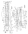
Figures 6 ,7 and 8 of the drawings another embodiment of display of the present invention is there shown and generally designated by the numeral 80. - As before the
display 80 includesoptical waveguide 21,light sources 25 that are installed proximate thewide edge 26 of thewaveguide 21 andmicro-prisms 32 are constructed atupper surface 30 and, as generally shown inFigure 6 , extend between side surfaces 28 and 29 of thewaveguide 21. Thedisplay 80 further includes a plurality of tiltingmicro-shutters 81 that are constructed betweenmicro-prisms 32. InFigure 7 , one column of the tilting micro-shutters is designated as 81a, 81b, and 81c.Figure 6 also illustrates a section of acover assembly 84. More detailed construction of thecover assembly 84 is illustrated inFigure 8 . - Now referring to
Figure 8 of the drawings where more details of multilayer optical coatings are shown. The first layer is alight reflecting layer 35 constructed from metal or multilayer dielectric materials on theupper surface 30 of thewaveguide 21. Thelight reflecting layer 35 is patterned to form plurality oflight reflecting regions 36 andlight transmitting regions 37. The second optical layer is alight transmitting layer 39 formed from a fluoropolymer or other substantially transparent material having a refractive index n3 with a value between approximately 1.3 and approximately 1.4. Thelight transmitting layer 39 is formed only in thelight transmitting regions 37 as shown inFigure 8 on theupper surface 30 of thewaveguide 21. Also thelight transmitting layer 39 may be a continuous layer formed between thelight reflecting layer 35 andupper surface 30 of thewaveguide 21. The third optical layer is a light absorbinglayer 82 formed from a dielectric material onlight reflecting layer 35 and is patterned to partially coverlight reflecting layer 35. A black oxide layer may be formed on upper surface oflight reflecting layer 35 instead of light absorbinglayer 82. Also thelight absorbing layer 82 may be replaced with a light absorbing film and placed below thelower surface 31 of thewaveguide 21. - Further illustrated in
Figure 8 are micro-prisms 32. Each micro-prism 32 comprises alight input facet 41 which is optically coupled to theupper surface 30 ofwaveguide 21 vialight transmitting layer 39 and alight exit facet 42 which is inclined with respect to theupper surface 30 ofwaveguide 21 and forms anangle 23 with a value between approximately 45 degrees to approximately 65 degrees. Micro-prisms 32 further include afacet 43 which is inclined opposite to thelight exit facet 42 and anupper facet 47 which is generally parallel to thelight input facet 41. -
Figure 8 also illustrates one of the tilting micro-shutters 81b which typifies the construction of each of the micro-shutters of the present form of the invention. Micro-shutter 81b comprises a thin aluminum alloy elastic film that is affixed to theupper facet 47 of micro-prism 32b and it tilts in two directions at aboutaxis 85 that is substantially parallel to theupper surface 30 of thewaveguide 21. For absorbing light, a black oxide layer or a black polymer film may be formed on surfaces ofmicro-shutters 81. - Further illustrated in
Figure 8 is acover assembly 84 which is affixed to theupper surface 30 ofwaveguide 21 with spacers 83 (seeFigure 7 ). The construction of thecover assembly 84 is similar to thecover assembly 34 that was described above. - In the present form of the invention, the tilting
micro-shutters 81 operate by electrostatic attraction force. The conductivelight reflecting layer 35 and conductivelight absorbing layer 51 act as fixed electrodes for the tiltingmicro-shutters 81. - When a suitable voltage is applied between the conductive
light reflecting layer 35 and a micro-shutter 81, the micro-shutter tilts down by electrostatic attraction force. When a suitable voltage is applied between the conductivelight absorbing layer 51 and a micro-shutter 81, the micro-shutter tilts up by electrostatic attraction force. - To prevent micro-shutter stiction, a small gap is required between the edge of the micro-shutters and the landing surfaces. This may be realized by constructing small spacers from a low friction material on landing surfaces or extending small portions of micro-shutters along the edge so the entire edge of the micro-shutters do not touch the landing surfaces. Additionally the black polymer coatings on the micro-shutters may be formed from a non stick material.
- As best seen in
Figure 7 of the drawings, light rays 55 entering from thewide edge 26 of thewaveguide 21 reflect from theupper surface 30 and thelower surface 31 by total internal reflections and change angles towards normal with respect to theupper surface 30. Light rays 55 exit thewaveguide 21 from the light transmitting regions 37 (Figure 8 ) when the incident angle is less than thecritical angle 38 defined by the refractive index n1 of thewaveguide 21 and refractive index n3 oflight transmitting layer 39. Light rays passing through thelight transmitting layer 39 enter the micro-prisms 32 from thelight input facet 41 and change the angle defined by the refractive index n2 of the micro-prisms. Light rays exit the micro-prisms from thelight exit facets 42. - Depending on the positions of the tilting micro-shutters, light rays are absorbed, or directed to the viewer.
- When a tilting micro-shutter is in the up position, such as
micro-shutter 81b (Figure 7 ), most light rays exiting fromlight exit facet 42 ofmicro-prisms 32 are absorbed in light absorber coatings ofmicro-shutters 81. Any light reflected from the lower surface of the micro-shutters 81 will be absorbed in thelight absorbing layer 40. - When a micro-shutter is tilted down, such as micro-shutters 81a and 81c, most light rays exiting from
light exit facet 42 ofmicro-prisms 32 exit thedisplay 80 from displaylight exit regions 48 and are directed to the viewer. - The above described displays will work with infrared, visible and ultraviolet light sources and combinations thereof.
- Depending on the display size and resolution, each picture element of the display panel may include several tilting light modulators. Reducing the size of individual light modulators helps to reduce the required electrostatic actuation voltages.
- Also, light modulators for each picture element may be grouped to modulate different levels of light when suitable voltage is applied between the fixed electrodes and a selected group of light modulators. This reduces the display addressing constraints. For example, each picture element may include 7 light modulators grouped in quantities of 1, 2 and 4 and selectively addressed to modulate 8 levels of light. Additionally, temporal artifacts inherent in pulse-width-modulation displays are reduced.
- To increase the efficiency and reduce light scattering various antireflection coatings may be applied to surfaces where light transitions between two different materials.
- Dichroic layers that comprise a low pass filter for the Blue color and a high pass filter for the Red color may be formed to overlap in the
light reflecting regions 36. - To simplify manufacturing of micro-mirrors, micro-prisms may be split to lower and upper sections and micro-mirrors may be formed on a flat surface after forming the lower sections of micro-prisms.
- Having now described the invention in detail in accordance with the requirements of the patent statutes, those skilled in this art will have no difficulty in making changes and modifications in the individual parts or their relative assembly in order to meet specific requirements or conditions. Such changes and modification may be made without departing from the following claims.
Claims (15)
- A display (20, 80) comprising:(a) a light source for generating light(25);(b) an optical waveguide (21) for receiving and distributing said light, said optical waveguide having a refractive index n1, an upper surface (30) and a spaced-apart lower surface (31) converging with said upper surface;(c) a plurality of spaced-apart micro-prisms (32), each said micro-prism comprising: a refractive index n2, a light input facet (41) optically coupled to said upper surface of said optical waveguide via an optical layer (39) having a refractive index n3 which is less than said refractive index n2 and said refractive index n1 and greater than 1, and a light exit facet(42) located above said upper surface of said optical waveguide and inclined opposite to said lower surface of said optical waveguide; and
characterized by(d) a plurality of tilting light modulators (33, 81), each said tilting light modulator having a tilt axis (50, 85) substantially parallel to said upper surface of said optical waveguide and located between said spaced-apart micro-prisms;wherein most light rays exiting each said light exit facet of said micro-prisms are directed to the viewer when a respective tilting light modulator is at a first position or absorbed in a light absorber (40, 82) when said respective tilting light modulator is at a second position. - A display according claim 1 further includes a light reflecting layer (35) disposed proximate said upper surface of said optical waveguide, constructed from a metal having a specular light reflecting lower surface and a light absorbing upper surface.
- A display according claim 2 wherein said optical layer is formed between said light reflecting layer and said upper surface of said optical waveguide.
- A display according claim 2 or 3 wherein each said tilting light modulator is actuated by electrostatic force and said light reflecting layer functions as a fixed electrode for said tilting light modulators.
- A display according any of preceding claim wherein each said tilting light modulator tilts in two directions from said tilt axis.
- A display according any of preceding claim wherein said plurality of tilting light modulators are divided to a plurality of groups and light modulators of each said group tilt simultaneously by an electrostatic force.
- A display according any of preceding claim further includes a cover assembly (34, 84) comprising: a substantially transparent substrate (44), a light absorbing layer (51) and a light shaping diffuser layer (52) formed on said substantially transparent substrate.
- A display according any of preceding claim wherein said light exit facet of each said micro-prism forms an angle of between approximately 45 degrees and approximately 65 degrees relative to said upper surface of said optical waveguide.
- A display according any of preceding claim wherein said refractive index n1 is between approximately 1.45 and 1.6, and said refractive index n2 is between approximately 1.45 and 1.6, and said refractive index n3 is between approximately 1.3 and 1.4.
- A display according any of preceding claim wherein said light input facet of each said micro-prisms is optically coupled to said upper surface of said optical waveguide via a dichroic filter (75).
- A display according any of preceding claim wherein each said tilting light modulator is affixed on a selected one of said micro-prisms.
- A display according any of preceding claim wherein said optical layer is constructed from a fluoropolymer and each said micro-prism is constructed from a UV curing polymer.
- A display according any of preceding claim wherein each said tilting light modulator includes a light absorbing surfaces.
- A display according any of claim 1-12 further includes a light reflecting facet formed on a third facet of each of said micro-prisms and each said tilting light modulator comprises a specular light reflecting lower surface and a light absorbing upper surface.
- A display of claim 14 wherein said third facet of each of said micro-prisms forms an angle of between approximately 30 degrees and approximately 50 degrees relative to said upper surface of said optical waveguide.
Applications Claiming Priority (2)
| Application Number | Priority Date | Filing Date | Title |
|---|---|---|---|
| US12/583,156 US8177406B2 (en) | 2007-12-19 | 2009-08-13 | Display including waveguide, micro-prisms and micro-mirrors |
| US12/802,037 US8313226B2 (en) | 2010-05-28 | 2010-05-28 | Display including waveguide, micro-prisms and micro-shutters |
Publications (3)
| Publication Number | Publication Date |
|---|---|
| EP2284594A2 EP2284594A2 (en) | 2011-02-16 |
| EP2284594A3 EP2284594A3 (en) | 2011-10-26 |
| EP2284594B1 true EP2284594B1 (en) | 2013-11-27 |
Family
ID=43302415
Family Applications (1)
| Application Number | Title | Priority Date | Filing Date |
|---|---|---|---|
| EP10008145.4A Not-in-force EP2284594B1 (en) | 2009-08-13 | 2010-08-04 | Display including waveguide, micro-prisms and micro-mechanical light modulators |
Country Status (4)
| Country | Link |
|---|---|
| EP (1) | EP2284594B1 (en) |
| JP (1) | JP5634793B2 (en) |
| KR (1) | KR101699291B1 (en) |
| CN (1) | CN101995656B (en) |
Families Citing this family (9)
| Publication number | Priority date | Publication date | Assignee | Title |
|---|---|---|---|---|
| CN103454847B (en) * | 2012-05-29 | 2016-05-18 | 杨文君 | Slab guide display and system |
| CN107577043B (en) * | 2016-07-04 | 2021-10-08 | 爱德华·帕克奇亚恩 | MEMS light modulator for display |
| CN107577040B (en) * | 2016-07-04 | 2022-03-01 | 爱德华·帕克奇亚恩 | Light modulator for MEMS display |
| KR102590788B1 (en) * | 2016-07-04 | 2023-10-17 | 에드워드 파크얀 | Mems display |
| CN107577041B (en) * | 2016-07-04 | 2022-05-31 | 爱德华·帕克奇亚恩 | MEMS display |
| CN107577042A (en) * | 2016-07-04 | 2018-01-12 | 爱德华·帕克奇亚恩 | Mems display |
| CN116841075A (en) * | 2017-05-08 | 2023-10-03 | 瑞尔D斯帕克有限责任公司 | Optical stack for directional display |
| CN110208896B (en) * | 2019-05-21 | 2024-03-12 | 安徽省东超科技有限公司 | Novel optical waveguide and screen using same |
| CN116931336A (en) * | 2022-04-12 | 2023-10-24 | 深圳市中光工业技术研究院 | Integrated optical coupling switch |
Family Cites Families (14)
| Publication number | Priority date | Publication date | Assignee | Title |
|---|---|---|---|---|
| US5428468A (en) * | 1993-11-05 | 1995-06-27 | Alliedsignal Inc. | Illumination system employing an array of microprisms |
| US5914760A (en) * | 1996-06-21 | 1999-06-22 | Casio Computer Co., Ltd. | Surface light source device and liquid crystal display device using the same |
| JP3787983B2 (en) * | 1997-06-18 | 2006-06-21 | セイコーエプソン株式会社 | Optical switching element, image display device, and projection device |
| CN100343717C (en) * | 1998-09-24 | 2007-10-17 | 反射公司 | Double-layer dielectric reflective space optical modulator with self-limiting micro-mechanical component |
| JP3890777B2 (en) * | 1998-10-13 | 2007-03-07 | セイコーエプソン株式会社 | Micromachine, method for manufacturing micromachine, and spatial light modulator |
| JP3411014B2 (en) * | 2000-11-02 | 2003-05-26 | 株式会社東芝 | Inductive charge mirror |
| JP2004212673A (en) * | 2002-12-27 | 2004-07-29 | Fuji Photo Film Co Ltd | Planar display device and its driving method |
| US7274347B2 (en) * | 2003-06-27 | 2007-09-25 | Texas Instruments Incorporated | Prevention of charge accumulation in micromirror devices through bias inversion |
| US7417782B2 (en) * | 2005-02-23 | 2008-08-26 | Pixtronix, Incorporated | Methods and apparatus for spatial light modulation |
| JP2006108033A (en) * | 2004-10-08 | 2006-04-20 | Mitsubishi Rayon Co Ltd | Tandem type surface light source device |
| JP4329703B2 (en) * | 2005-02-16 | 2009-09-09 | セイコーエプソン株式会社 | Lighting device, electro-optical device, electronic equipment |
| GB2428303A (en) | 2005-07-08 | 2007-01-24 | Sharp Kk | An illumination system for switching a display between a public and private viewing mode |
| US7876489B2 (en) * | 2006-06-05 | 2011-01-25 | Pixtronix, Inc. | Display apparatus with optical cavities |
| US8087811B2 (en) * | 2007-12-19 | 2012-01-03 | Edward Pakhchyan | Display |
-
2010
- 2010-08-04 EP EP10008145.4A patent/EP2284594B1/en not_active Not-in-force
- 2010-08-12 JP JP2010180901A patent/JP5634793B2/en active Active
- 2010-08-12 CN CN201010255430.XA patent/CN101995656B/en active Active
- 2010-08-13 KR KR1020100078123A patent/KR101699291B1/en active IP Right Grant
Also Published As
| Publication number | Publication date |
|---|---|
| CN101995656B (en) | 2015-01-14 |
| KR20110017349A (en) | 2011-02-21 |
| KR101699291B1 (en) | 2017-01-24 |
| EP2284594A2 (en) | 2011-02-16 |
| CN101995656A (en) | 2011-03-30 |
| JP5634793B2 (en) | 2014-12-03 |
| JP2011059679A (en) | 2011-03-24 |
| EP2284594A3 (en) | 2011-10-26 |
Similar Documents
| Publication | Publication Date | Title |
|---|---|---|
| US8313226B2 (en) | Display including waveguide, micro-prisms and micro-shutters | |
| EP2284594B1 (en) | Display including waveguide, micro-prisms and micro-mechanical light modulators | |
| US7995261B2 (en) | Electromechanical display and backlight | |
| US11874477B2 (en) | Wearable data display | |
| EP0750209B1 (en) | Light guiding sheet | |
| US7903317B2 (en) | Transflective electrowetting display device | |
| KR101324300B1 (en) | Methods and apparatus for spatial light modulation | |
| CN108319070B (en) | Display device and display method thereof | |
| TWI402598B (en) | Optical films for controlling angular characteristics of displays | |
| CN110214287B (en) | Multi-view backlighting with color customized emission patterns | |
| US8087811B2 (en) | Display | |
| WO2017039756A1 (en) | Time-modulated backlight and multiview display using same | |
| CN102636872A (en) | Touchscreens for displays | |
| KR20100094545A (en) | Light illumination of displays with front light guide and coupling elements | |
| CA3064551C (en) | Multiview backlight, multiview display and method employing offset multibeam elements | |
| US8177406B2 (en) | Display including waveguide, micro-prisms and micro-mirrors | |
| WO2008125926A1 (en) | Controllable light-guide and display device | |
| CN106652960A (en) | Display panel, display device and control method thereof | |
| US7883219B2 (en) | System and method for displaying images | |
| CN110737138B (en) | Display panel, display device and control method thereof | |
| CN113439228A (en) | Horizontal parallax multiview display with light control film and method | |
| JP2020013067A (en) | Optical structure and display device | |
| WO2020203313A1 (en) | Display device and lens array | |
| CN117055259A (en) | Optical film group, display panel and display device |
Legal Events
| Date | Code | Title | Description |
|---|---|---|---|
| PUAI | Public reference made under article 153(3) epc to a published international application that has entered the european phase |
Free format text: ORIGINAL CODE: 0009012 |
|
| AK | Designated contracting states |
Kind code of ref document: A2 Designated state(s): AL AT BE BG CH CY CZ DE DK EE ES FI FR GB GR HR HU IE IS IT LI LT LU LV MC MK MT NL NO PL PT RO SE SI SK SM TR |
|
| AX | Request for extension of the european patent |
Extension state: BA ME RS |
|
| PUAL | Search report despatched |
Free format text: ORIGINAL CODE: 0009013 |
|
| AK | Designated contracting states |
Kind code of ref document: A3 Designated state(s): AL AT BE BG CH CY CZ DE DK EE ES FI FR GB GR HR HU IE IS IT LI LT LU LV MC MK MT NL NO PL PT RO SE SI SK SM TR |
|
| AX | Request for extension of the european patent |
Extension state: BA ME RS |
|
| RIC1 | Information provided on ipc code assigned before grant |
Ipc: G02B 26/08 20060101AFI20110921BHEP Ipc: G02B 5/04 20060101ALI20110921BHEP Ipc: G02B 6/00 20060101ALI20110921BHEP |
|
| 17P | Request for examination filed |
Effective date: 20120425 |
|
| RIC1 | Information provided on ipc code assigned before grant |
Ipc: G02B 5/04 20060101ALI20130502BHEP Ipc: F21V 8/00 20060101ALI20130502BHEP Ipc: G09G 3/34 20060101ALI20130502BHEP Ipc: G02B 6/00 20060101ALI20130502BHEP Ipc: G09G 3/00 20060101ALI20130502BHEP Ipc: G02B 26/08 20060101AFI20130502BHEP |
|
| GRAP | Despatch of communication of intention to grant a patent |
Free format text: ORIGINAL CODE: EPIDOSNIGR1 |
|
| INTG | Intention to grant announced |
Effective date: 20130708 |
|
| GRAS | Grant fee paid |
Free format text: ORIGINAL CODE: EPIDOSNIGR3 |
|
| GRAA | (expected) grant |
Free format text: ORIGINAL CODE: 0009210 |
|
| RAP1 | Party data changed (applicant data changed or rights of an application transferred) |
Owner name: PAKHCHYAN, SYUZI Owner name: MESROPIAN, HAIK Owner name: PAKHCHYAN, EDWARD |
|
| RIN1 | Information on inventor provided before grant (corrected) |
Inventor name: MESROPIAN, HAIK Inventor name: PAKHCHYAN, EDWARD Inventor name: PAKHCHYAN, SYUZI |
|
| AK | Designated contracting states |
Kind code of ref document: B1 Designated state(s): AL AT BE BG CH CY CZ DE DK EE ES FI FR GB GR HR HU IE IS IT LI LT LU LV MC MK MT NL NO PL PT RO SE SI SK SM TR |
|
| REG | Reference to a national code |
Ref country code: GB Ref legal event code: FG4D |
|
| REG | Reference to a national code |
Ref country code: CH Ref legal event code: EP |
|
| REG | Reference to a national code |
Ref country code: AT Ref legal event code: REF Ref document number: 642944 Country of ref document: AT Kind code of ref document: T Effective date: 20131215 |
|
| REG | Reference to a national code |
Ref country code: IE Ref legal event code: FG4D |
|
| REG | Reference to a national code |
Ref country code: DE Ref legal event code: R096 Ref document number: 602010011997 Country of ref document: DE Effective date: 20140123 |
|
| REG | Reference to a national code |
Ref country code: NL Ref legal event code: VDEP Effective date: 20131127 |
|
| REG | Reference to a national code |
Ref country code: AT Ref legal event code: MK05 Ref document number: 642944 Country of ref document: AT Kind code of ref document: T Effective date: 20131127 |
|
| REG | Reference to a national code |
Ref country code: LT Ref legal event code: MG4D |
|
| PG25 | Lapsed in a contracting state [announced via postgrant information from national office to epo] |
Ref country code: SE Free format text: LAPSE BECAUSE OF FAILURE TO SUBMIT A TRANSLATION OF THE DESCRIPTION OR TO PAY THE FEE WITHIN THE PRESCRIBED TIME-LIMIT Effective date: 20131127 Ref country code: IS Free format text: LAPSE BECAUSE OF FAILURE TO SUBMIT A TRANSLATION OF THE DESCRIPTION OR TO PAY THE FEE WITHIN THE PRESCRIBED TIME-LIMIT Effective date: 20140327 Ref country code: NO Free format text: LAPSE BECAUSE OF FAILURE TO SUBMIT A TRANSLATION OF THE DESCRIPTION OR TO PAY THE FEE WITHIN THE PRESCRIBED TIME-LIMIT Effective date: 20140227 Ref country code: NL Free format text: LAPSE BECAUSE OF FAILURE TO SUBMIT A TRANSLATION OF THE DESCRIPTION OR TO PAY THE FEE WITHIN THE PRESCRIBED TIME-LIMIT Effective date: 20131127 Ref country code: FI Free format text: LAPSE BECAUSE OF FAILURE TO SUBMIT A TRANSLATION OF THE DESCRIPTION OR TO PAY THE FEE WITHIN THE PRESCRIBED TIME-LIMIT Effective date: 20131127 Ref country code: LT Free format text: LAPSE BECAUSE OF FAILURE TO SUBMIT A TRANSLATION OF THE DESCRIPTION OR TO PAY THE FEE WITHIN THE PRESCRIBED TIME-LIMIT Effective date: 20131127 Ref country code: HR Free format text: LAPSE BECAUSE OF FAILURE TO SUBMIT A TRANSLATION OF THE DESCRIPTION OR TO PAY THE FEE WITHIN THE PRESCRIBED TIME-LIMIT Effective date: 20131127 |
|
| PG25 | Lapsed in a contracting state [announced via postgrant information from national office to epo] |
Ref country code: ES Free format text: LAPSE BECAUSE OF FAILURE TO SUBMIT A TRANSLATION OF THE DESCRIPTION OR TO PAY THE FEE WITHIN THE PRESCRIBED TIME-LIMIT Effective date: 20131127 Ref country code: LV Free format text: LAPSE BECAUSE OF FAILURE TO SUBMIT A TRANSLATION OF THE DESCRIPTION OR TO PAY THE FEE WITHIN THE PRESCRIBED TIME-LIMIT Effective date: 20131127 Ref country code: CY Free format text: LAPSE BECAUSE OF FAILURE TO SUBMIT A TRANSLATION OF THE DESCRIPTION OR TO PAY THE FEE WITHIN THE PRESCRIBED TIME-LIMIT Effective date: 20131127 Ref country code: AT Free format text: LAPSE BECAUSE OF FAILURE TO SUBMIT A TRANSLATION OF THE DESCRIPTION OR TO PAY THE FEE WITHIN THE PRESCRIBED TIME-LIMIT Effective date: 20131127 Ref country code: BE Free format text: LAPSE BECAUSE OF FAILURE TO SUBMIT A TRANSLATION OF THE DESCRIPTION OR TO PAY THE FEE WITHIN THE PRESCRIBED TIME-LIMIT Effective date: 20131127 |
|
| PG25 | Lapsed in a contracting state [announced via postgrant information from national office to epo] |
Ref country code: PT Free format text: LAPSE BECAUSE OF FAILURE TO SUBMIT A TRANSLATION OF THE DESCRIPTION OR TO PAY THE FEE WITHIN THE PRESCRIBED TIME-LIMIT Effective date: 20140327 |
|
| PG25 | Lapsed in a contracting state [announced via postgrant information from national office to epo] |
Ref country code: EE Free format text: LAPSE BECAUSE OF FAILURE TO SUBMIT A TRANSLATION OF THE DESCRIPTION OR TO PAY THE FEE WITHIN THE PRESCRIBED TIME-LIMIT Effective date: 20131127 |
|
| REG | Reference to a national code |
Ref country code: DE Ref legal event code: R097 Ref document number: 602010011997 Country of ref document: DE |
|
| PG25 | Lapsed in a contracting state [announced via postgrant information from national office to epo] |
Ref country code: CZ Free format text: LAPSE BECAUSE OF FAILURE TO SUBMIT A TRANSLATION OF THE DESCRIPTION OR TO PAY THE FEE WITHIN THE PRESCRIBED TIME-LIMIT Effective date: 20131127 Ref country code: PL Free format text: LAPSE BECAUSE OF FAILURE TO SUBMIT A TRANSLATION OF THE DESCRIPTION OR TO PAY THE FEE WITHIN THE PRESCRIBED TIME-LIMIT Effective date: 20131127 Ref country code: SK Free format text: LAPSE BECAUSE OF FAILURE TO SUBMIT A TRANSLATION OF THE DESCRIPTION OR TO PAY THE FEE WITHIN THE PRESCRIBED TIME-LIMIT Effective date: 20131127 Ref country code: RO Free format text: LAPSE BECAUSE OF FAILURE TO SUBMIT A TRANSLATION OF THE DESCRIPTION OR TO PAY THE FEE WITHIN THE PRESCRIBED TIME-LIMIT Effective date: 20131127 |
|
| PG25 | Lapsed in a contracting state [announced via postgrant information from national office to epo] |
Ref country code: DK Free format text: LAPSE BECAUSE OF FAILURE TO SUBMIT A TRANSLATION OF THE DESCRIPTION OR TO PAY THE FEE WITHIN THE PRESCRIBED TIME-LIMIT Effective date: 20131127 |
|
| PLBE | No opposition filed within time limit |
Free format text: ORIGINAL CODE: 0009261 |
|
| STAA | Information on the status of an ep patent application or granted ep patent |
Free format text: STATUS: NO OPPOSITION FILED WITHIN TIME LIMIT |
|
| 26N | No opposition filed |
Effective date: 20140828 |
|
| REG | Reference to a national code |
Ref country code: DE Ref legal event code: R097 Ref document number: 602010011997 Country of ref document: DE Effective date: 20140828 |
|
| PG25 | Lapsed in a contracting state [announced via postgrant information from national office to epo] |
Ref country code: SI Free format text: LAPSE BECAUSE OF FAILURE TO SUBMIT A TRANSLATION OF THE DESCRIPTION OR TO PAY THE FEE WITHIN THE PRESCRIBED TIME-LIMIT Effective date: 20131127 |
|
| PG25 | Lapsed in a contracting state [announced via postgrant information from national office to epo] |
Ref country code: MC Free format text: LAPSE BECAUSE OF FAILURE TO SUBMIT A TRANSLATION OF THE DESCRIPTION OR TO PAY THE FEE WITHIN THE PRESCRIBED TIME-LIMIT Effective date: 20131127 Ref country code: LU Free format text: LAPSE BECAUSE OF FAILURE TO SUBMIT A TRANSLATION OF THE DESCRIPTION OR TO PAY THE FEE WITHIN THE PRESCRIBED TIME-LIMIT Effective date: 20140804 |
|
| REG | Reference to a national code |
Ref country code: CH Ref legal event code: PL |
|
| PG25 | Lapsed in a contracting state [announced via postgrant information from national office to epo] |
Ref country code: LI Free format text: LAPSE BECAUSE OF NON-PAYMENT OF DUE FEES Effective date: 20140831 Ref country code: IT Free format text: LAPSE BECAUSE OF FAILURE TO SUBMIT A TRANSLATION OF THE DESCRIPTION OR TO PAY THE FEE WITHIN THE PRESCRIBED TIME-LIMIT Effective date: 20131127 Ref country code: CH Free format text: LAPSE BECAUSE OF NON-PAYMENT OF DUE FEES Effective date: 20140831 |
|
| REG | Reference to a national code |
Ref country code: IE Ref legal event code: MM4A |
|
| PG25 | Lapsed in a contracting state [announced via postgrant information from national office to epo] |
Ref country code: IE Free format text: LAPSE BECAUSE OF NON-PAYMENT OF DUE FEES Effective date: 20140804 |
|
| PG25 | Lapsed in a contracting state [announced via postgrant information from national office to epo] |
Ref country code: SM Free format text: LAPSE BECAUSE OF FAILURE TO SUBMIT A TRANSLATION OF THE DESCRIPTION OR TO PAY THE FEE WITHIN THE PRESCRIBED TIME-LIMIT Effective date: 20131127 |
|
| PG25 | Lapsed in a contracting state [announced via postgrant information from national office to epo] |
Ref country code: MT Free format text: LAPSE BECAUSE OF FAILURE TO SUBMIT A TRANSLATION OF THE DESCRIPTION OR TO PAY THE FEE WITHIN THE PRESCRIBED TIME-LIMIT Effective date: 20131127 Ref country code: GR Free format text: LAPSE BECAUSE OF FAILURE TO SUBMIT A TRANSLATION OF THE DESCRIPTION OR TO PAY THE FEE WITHIN THE PRESCRIBED TIME-LIMIT Effective date: 20140228 Ref country code: BG Free format text: LAPSE BECAUSE OF FAILURE TO SUBMIT A TRANSLATION OF THE DESCRIPTION OR TO PAY THE FEE WITHIN THE PRESCRIBED TIME-LIMIT Effective date: 20131127 |
|
| PG25 | Lapsed in a contracting state [announced via postgrant information from national office to epo] |
Ref country code: HU Free format text: LAPSE BECAUSE OF FAILURE TO SUBMIT A TRANSLATION OF THE DESCRIPTION OR TO PAY THE FEE WITHIN THE PRESCRIBED TIME-LIMIT; INVALID AB INITIO Effective date: 20100804 Ref country code: TR Free format text: LAPSE BECAUSE OF FAILURE TO SUBMIT A TRANSLATION OF THE DESCRIPTION OR TO PAY THE FEE WITHIN THE PRESCRIBED TIME-LIMIT Effective date: 20131127 |
|
| REG | Reference to a national code |
Ref country code: FR Ref legal event code: PLFP Year of fee payment: 7 |
|
| PGFP | Annual fee paid to national office [announced via postgrant information from national office to epo] |
Ref country code: DE Payment date: 20160726 Year of fee payment: 7 Ref country code: GB Payment date: 20160803 Year of fee payment: 7 |
|
| PGFP | Annual fee paid to national office [announced via postgrant information from national office to epo] |
Ref country code: FR Payment date: 20160729 Year of fee payment: 7 |
|
| REG | Reference to a national code |
Ref country code: DE Ref legal event code: R119 Ref document number: 602010011997 Country of ref document: DE |
|
| GBPC | Gb: european patent ceased through non-payment of renewal fee |
Effective date: 20170804 |
|
| REG | Reference to a national code |
Ref country code: FR Ref legal event code: ST Effective date: 20180430 |
|
| PG25 | Lapsed in a contracting state [announced via postgrant information from national office to epo] |
Ref country code: MK Free format text: LAPSE BECAUSE OF FAILURE TO SUBMIT A TRANSLATION OF THE DESCRIPTION OR TO PAY THE FEE WITHIN THE PRESCRIBED TIME-LIMIT Effective date: 20131127 |
|
| PG25 | Lapsed in a contracting state [announced via postgrant information from national office to epo] |
Ref country code: DE Free format text: LAPSE BECAUSE OF NON-PAYMENT OF DUE FEES Effective date: 20180301 Ref country code: GB Free format text: LAPSE BECAUSE OF NON-PAYMENT OF DUE FEES Effective date: 20170804 |
|
| PG25 | Lapsed in a contracting state [announced via postgrant information from national office to epo] |
Ref country code: FR Free format text: LAPSE BECAUSE OF NON-PAYMENT OF DUE FEES Effective date: 20170831 |
|
| PG25 | Lapsed in a contracting state [announced via postgrant information from national office to epo] |
Ref country code: AL Free format text: LAPSE BECAUSE OF FAILURE TO SUBMIT A TRANSLATION OF THE DESCRIPTION OR TO PAY THE FEE WITHIN THE PRESCRIBED TIME-LIMIT Effective date: 20131127 |