EP2249531A2 - Radio receiver for different data rates - Google Patents
Radio receiver for different data rates Download PDFInfo
- Publication number
- EP2249531A2 EP2249531A2 EP10174059A EP10174059A EP2249531A2 EP 2249531 A2 EP2249531 A2 EP 2249531A2 EP 10174059 A EP10174059 A EP 10174059A EP 10174059 A EP10174059 A EP 10174059A EP 2249531 A2 EP2249531 A2 EP 2249531A2
- Authority
- EP
- European Patent Office
- Prior art keywords
- data rate
- signal processing
- signal
- digital
- frequency
- Prior art date
- Legal status (The legal status is an assumption and is not a legal conclusion. Google has not performed a legal analysis and makes no representation as to the accuracy of the status listed.)
- Withdrawn
Links
Images


Classifications
-
- H—ELECTRICITY
- H04—ELECTRIC COMMUNICATION TECHNIQUE
- H04L—TRANSMISSION OF DIGITAL INFORMATION, e.g. TELEGRAPHIC COMMUNICATION
- H04L27/00—Modulated-carrier systems
- H04L27/18—Phase-modulated carrier systems, i.e. using phase-shift keying
- H04L27/22—Demodulator circuits; Receiver circuits
- H04L27/233—Demodulator circuits; Receiver circuits using non-coherent demodulation
- H04L27/2338—Demodulator circuits; Receiver circuits using non-coherent demodulation using sampling
-
- H—ELECTRICITY
- H04—ELECTRIC COMMUNICATION TECHNIQUE
- H04L—TRANSMISSION OF DIGITAL INFORMATION, e.g. TELEGRAPHIC COMMUNICATION
- H04L25/00—Baseband systems
- H04L25/02—Details ; arrangements for supplying electrical power along data transmission lines
Landscapes
- Engineering & Computer Science (AREA)
- Computer Networks & Wireless Communication (AREA)
- Signal Processing (AREA)
- Power Engineering (AREA)
- Digital Transmission Methods That Use Modulated Carrier Waves (AREA)
- Circuits Of Receivers In General (AREA)
- Superheterodyne Receivers (AREA)
- Analogue/Digital Conversion (AREA)
Abstract
Description
- The present invention relates to a radio receiver and to methods of operation thereof. There will be described below, by way of example in illustration of the invention a low-power-consumption radio receiver which is able to receive a plurality of channels at different frequencies and which has a reduced power consumption.
- Various radio receivers, such as portable telephones, and mobile computers have been proposed. Recently, a software radio system has been proposed and developed.
- This software radio system enables the same device to perform communications at different frequencies, or by employing different communication schemes, as a result of making software changes.
- A reduction in power consumption presents a significant challenge for a radio receiver, and more specifically, for a portable radio receiver, and demands have arisen for the development of a lower-power consumption radio receiver.
- A feature of an arrangement to be described, by way of example in illustration of the present invention is that it enables a low-power-consumption radio receiver which reduces power consumption to be provided by decreasing the data rate of received data.
- In a particular radio receiver to be described by way of example in illustration of the present invention, there is a device for decreasing the data rate of received data in accordance with the channel frequency of the received data, and a device for performing signal processing of the received data whose data rate has been decreased.
- There will be described below, by way of example in illustration of the invention, a radio receiver which is capable of receiving a plurality of different channel frequencies, the receiver including an A/D converter for A/D-converting a received signal, a signal processing section for performing digital signal processing of a signal which has undergone digital conversion in the A/D converter, and either a sampling frequency changing device for changing the sampling frequency in the A/D converter in accordance with the frequency of the received signal, or a data rate changing device for changing the data rate of the signal which is input to the signal processing section and which has undergone digital conversion.
- A power consumption reducing method for a radio receiver to be described below, by way of example in illustration of the invention includes the steps of decreasing the data rate of received data, and performing signal processing of the received data whose data rate has been decreased.
- Power consumption poses a significant challenge to portable telephones, mobile computers, and the like. It is known that power consumption can be reduced in signal processing by decreasing the clock speed used for the processing. In the particular arrangements to be described by way of example in illustration of the present invention, the clock speed required for signal processing is decreased by decreasing the data rate, thereby realizing a power consumption reducing effect.
- The following description and drawings disclose, by means of examples, the invention which is characterised in the appended claims, whose terms determine the extent of the protection conferred hereby.
- In the drawings:
-
Fig. 1 is a block schematic diagram showing the main part of a radio receiver, -
Figs. 2A to 2G are timing charts for explaining a variable sampling frequency decreasing method for use in the receiver shown inFig. 1 , -
Figs. 3A to 3G are timing charts for explaining another variable sampling frequency decreasing method for use in the receiver shown inFig. 1 , -
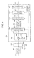
Fig. 4 is a block schematic diagram showing the main part of another radio receiver, and -
Figs. 5A to 5D are timing charts for explaining a variable sampling frequency decreasing method for use in the receiver shown inFig. 4 . - Referring to
Fig. 1 , the radio receiver includes ananalog filter 101 for limiting an input signal band, an A/D converter 102 for sampling an input signal and converting it into a digital signal, anoscillator 103 for supplying a clock sampling signal to the A/D converter 102, and asignal processing section 104. - The
signal processing section 104 includes a DSP or CPU, a ROM, and a RAM. This section may be implemented by software or hardware by using a logic circuit, such as a gate array or an FPGA. - The
signal processing section 104 includes aquadrature demodulation section 105 for quadrature-demodulatingdigital data 118 received from the A/D converter 102, a first datarate changing section 110 for changing the data rate of I and Q signals after quadrature demodulation, a digital filter section 111 for extracting a channel to be received, a second datarate changing section 112, ademodulation section 113, a next-stagesignal processing section 114 for performing conventional signal processing such as decoding, and acontrol section 115. - The
quadrature demodulation section 105 includesmixers digital oscillator 109, and a π/2shift section 108. - The operation of the receiver shown in
Fig. 1 will now be described with reference toFigs. 2A to 2G , orFigs. 3A to 3G . - Assume that in a radio receiver capable of receiving several different channel frequencies in a receivable frequency band (to be referred to as a receivable band hereinafter) B, a given channel frequency fIFn (n is an arbitrary number) is to be received. The operation of part of the receiving section shown in
Fig. 1 will now be described. - An
analog input signal 116 is band-limited by theanalog filter 101. Theanalog filter 101 is a filter that passes the receivable band B. - The band-
limited signal 117 which is output from thefilter 101 is sampled and quantized by the A/D converter 102 using a sampling clock signal generated by theoscillator 103 and having a sampling frequency fs. According to the Nyquist theorem, the sampling frequency fs must be two times, or more, that of the receivable band B. The data rate of thesignal 118 output from theconverter 102 is the sampling frequency fs. - The
signal processing section 104 includes a DSP or CPU, a ROM, and a RAM when it has a software configuration. When this section is to have a logic configuration, the same functions are implemented by a gate array, FPGA, or the like. - The sampled signal 118 (data rate fs) which is output from the A/
D converter 102 is input to thesignal processing section 104. - To quadrature-demodulate the received channel frequency fIFn, the
control section 115 controls thequadrature demodulation section 105 constituted by themixers digital oscillator 109, and the π/2shift section 108. More specifically, thecontrol section 115 controls thedigital oscillator 109 to set the channel frequency to fIFn. - I and Q signals 119 and 120, after quadrature demodulation, are input to the first data
rate changing section 110. The first datarate changing section 110 performs a data rate changing operation on the basis of the information of the received channel fIFn under the control of thecontrol section 115, thereby setting the data rate ofoutput signals 121 and 122 to fsn (n is an arbitrary number). -
Signals rate changing section 112. Thecontrol section 115 controls the second datarate changing section 112 so that output signals 125 and 126 from the second datarate changing section 112 are set to a data rate fsaO. At this time, the data rate fsaO must satisfy the Nyquist condition with respect to a pass band B0 required for the reception. In this case, since thesignals 125 and 126 have been decreased to the baseband, fas0 is set under the condition that the data rate should be the pass band B0 or more. - These
signals 125 and 126 are input to thedemodulation section 113 to be demodulated. A demodulatedsignal 127 is transferred to the next-stagesignal processing section 114. The next-stagesignal processing section 114 is an existing signal processing section and has constituent elements for control by signal formats, decoding, speech reproduction, and the like. The next-stagesignal processing section 114 outputs sound, light, speech, FAX data, LCD data, PC data, and the like. - The data rate change operation in the second data
rate changing section 112 may be performed in the digital filter section 111. - A variable sampling frequency decreasing method employed with the arrangement shown in
Fig. 1 will now be described with reference toFigs. 2A to 2G . -
Fig. 2A shows the characteristics of an analog filter, including the receivable band B in its pass band and the reception channel frequencies fIF1 and fIF2, in the radio receiver ofFig. 1 . - In addition, a reference symbol Ba denotes the attenuation band of the
analog filter 101, which is set to a condition sufficient for cutting off interference by other channels, or noise, and to allow sufficient attenuation at frequencies that differ by a certain value or more. In this case, "sufficient attenuation" indicates a level at which aliasing noise (to be described later) is not superimposed on the necessary received signal sufficiently to degrade its sensitivity. - The received channel frequencies are the channel frequencies fIF1 and fIF2, and a larger frequency difference between the frequency at which a sufficient attenuation band is obtained and the channel frequency fIF1 is denoted by a reference symbol B1.
Fig. 2A also shows the sampling frequency fs in an A/D conversion in which the frequency must be two times, or more, the receivable band B, according to the Nyquist theorem. -
Fig. 2B shows a case in which the receiving channel for the frequency fIF1 is decreased to the baseband in thequadrature demodulation section 105. Since both the I andQ signals -
Fig. 2C shows thesignals 121 and 122 obtained when the data rate is changed to fs1 by the first datarate changing section 110. Aliasing noise is a general definition. In digital signal processing, a frequency 1/2 or more of the sampling frequency which falls out of the Nyquist definition becomes aliasing noise. Referring toFig. 2C , fs1 must be set to prevent aliasing noise from entering a pass band B0 required for reception. In this case, since the frequency separation B1 from the attenuation region shown inFigs. 2A and 2B becomes dominant, fs1 must satisfy the condition given by:
where B0 is the required pass band. -
Fig. 2D shows the case in which the required pass band B0 is extracted by the digital filter section 111, and the data rate is changed to fsa0 by the second datarate changing section 112. - Since the signals have already been band-limited by the digital filter section 111, even if the sampling rate is decreased to fsa0, two times, or more, the pass band B0, aliasing noise exerts no influence on the signals. These signals are the
signals 125 and 126, which are sent to thedemodulation section 113. - Reception of the channel frequency fIF2 in
Fig. 2E will be described next. Assume that a band with a larger frequency separation from the attenuation frequency of theanalog filter 101 is represented by B2 as in the case of the receiving channel frequency fIF1. - When the frequency is changed to the baseband frequency by quadrature demodulation, and the sampling frequency is decreased to fs2, as shown in
Fig. 2F , aliasing noise is produced as shown inFig. 2F . To prevent this aliasing noise from entering the required frequency band B0 of the reception channel frequency fIF2, the sampling frequency fs2 must satisfy the condition given:
where B0 is the required pass band. -
Fig. 2G shows a case in which the pass band B0 is extracted by the digital filter section 111, and the data rate is changed to fsa0 by the second datarate changing section 112. - Since the signals have already been band-limited by the digital filter section 111, even if the sampling rate is decreased to fsa0, aliasing noise exerts no influence on the signals. These signals are the
signals 125 and 126, which are sent to thedemodulation section 113. - As is obvious from these results, the data rates fs1 and fs2 of the
data 121 and 122 input to the digital filter section 111 can be effectively decreased on the basis of the respective received frequencies fIF1 and fIF2. - Another variable sampling frequency decreasing method in the embodiment shown in
Fig. 1 will be described with reference toFigs. 3A to 3G . -
Fig. 3A shows an analog filter band including the receivable band B and the sampling frequency fs in A/D conversion which is two or more times the receivable band B. In this case, a channel frequency fIF3 to be received is at the centre of the sufficient attenuation band Ba (≧ receivable band B) of the analog filter, whereas a channel frequency fIF4 is the lowest channel at the end of the receivable band B. -
Fig. 3B shows the I andQ signals quadrature demodulation section 105. -
Fig. 3C shows thesignals 121 and 122 obtained when the data rate is changed to fs3 in the first datarate changing section 110. That is, in the case shown inFig. 3C , to set fs3 so as to prevent aliasing noise from entering the required pass band B0, fs3 must satisfy the condition given by:
where Ba is the band with which the analog filter cannot satisfactorily cut off noise, and B0 is the required pass band. -
Fig. 3D shows the case in which the required pass band B0 is extracted by the digital filter section 111, and the data rate is changed to fsa0 by the second datarate changing section 112. - Since the signals have already been band-limited by the digital filter section 111, and fsa0 is higher than the pass band B0, even if the sampling rate is decreased to fsa0, no influences are exerted on the signals. These signals are the
signals 125 and 126, which are sent to thedemodulation section 113. - The reception of a channel frequency fIF4 shown in
Fig. 3E will be described next. -
Fig. 3F shows thesignals 121 and 122 obtained when the receiving channel frequency fIF4 is decreased to the baseband in thequadrature demodulation section 105, and the data rate is changed to fs4 in the first datarate changing section 110. As in the case shown inFig. 3C, Fig. 3F shows aliasing noise. That is, in the case shown inFig. 3F , fs4 is set under the condition given below to prevent aliasing noise from entering the required band B0:
where Ba is the band with which the analog filter cannot satisfactorily cut off noise, and B is the receivable band described above. -
Fig. 3G shows the case in which a required band is extracted by the digital filter section 111, and the data rate is changed to fsa0 by the second datarate changing section 112. - Since the signals have already been band-limited by the digital filter section 111, even if the sampling rate is decreased to fsa0, no influences are exerted on the signals. These signals are the
signals 125 and 126, which are sent to thedemodulation section 113. - As is obvious from these results, the sampling frequencies fs3 and fs4 of data input to the digital filter section 111 can be changed on the basis of the different receiving channel frequencies fIF3 and fIF3, and the operating frequency of the digital filter can be decreased independently. In this case, the data rates fs3 and fs4 based on the receiving channel frequencies fIF3 and fIF4 represent conditions for the minimum and maximum sampling frequencies. In addition, with regard to the condition of the receiving channel frequency fIF4 on which the sampling condition is maximized, there is no difference between the lowest channel frequency and the highest channel frequency in the receivable band B.
- Referring to
Fig. 4 , there is shown a radio receiver which includes ananalog filter 401 for band-limiting an input signal, an A/D converter 402 for sampling an input signal and converting it into a digital signal, anoscillator 403 for supplying a sampling clock to the A/D converter 402, and asignal processing section 404. - The
signal processing section 404 includes a DSP or CPU, a ROM, and a RAM. This section may be implemented by software or hardware by using a logic circuit such as a gate array or FPGA. - The
signal processing section 404 includes adown conversion section 405 for down-convertingdigital data 416 received from the A/D converter 402, a first datarate changing section 408 for changing the data rate of a signal which has undergone down-conversion, adigital filter section 409 for extracting a channel to be received, a second datarate changing section 410, ademodulation section 411, a next-stagesignal processing section 412 for performing conventional signal processing such as decoding, and acontrol section 413. - The down
conversion section 405 includes amixer 406 and adigital oscillator 407. -
Figs. 5A to 5D are timing charts for use in explaining a variable sampling frequency decreasing method used in the receiver shown inFig. 4 . - With reference to
Fig. 4 andFigs. 5A to 5D , assume that in a radio receiver capable of receiving several different channel frequencies in a receivable band B, a given channel frequency fIFn (n is an arbitrary number) is to be received. The operation to be carried out in part of the receiving section will now be described. - An
analog input signal 414 is band-limited by theanalog filter 401. Thisanalog filter 401 is a filter that passes the receivable band B. - A band-limited
signal 415 is sampled and quantized by the A/D converter 402 with a sampling clock generated by theoscillator 403 and having a sampling frequency fs. According to the Nyquist theorem, this sampling frequency fs needs to be two or more times the receivable band B. In this case, the data rate of asignal 416 is the sampling frequency fs. - The
signal processing section 404 includes a DSP or CPU, a ROM, and a RAM, when it has a software configuration. When this section is to have a logic configuration, the same function is implemented by a gate array, FPGA, or the like. - The signal 416 (data rate fs) sampled by the A/
D converter 402 is input to thesignal processing section 404. - First of all, the
control section 413 controls thedown conversion section 405 constituted by themixer 406 and thedigital oscillator 407 to down-convert the received channel frequency fIFn. More specifically, thecontrol section 413 controls thedigital oscillator 407 to set the frequency to fIFn-fIF0 or fIFn+fIF0. In this case, the frequency fIF0 is a frequency required for demodulation in thedemodulation section 411. - As a result, a
signal 417 having undergone down-conversion becomes fIF0. Thissignal 417 is input to the first datarate changing section 408. Thecontrol section 413 changes the data rate on the basis of the information of the received frequency fIFn. As a consequence, the data rate of anoutput signal 418 is set to fsbn (n is an arbitrary number). - A
signal 419 having passed through thedigital filter section 409 serving as a channel filter is input to the second datarate changing section 410.control section 413 controls the second datarate changing section 410 to make anoutput signal 420 from the second datarate changing section 410 have a data rate of fsb0. In this case, the data rate fsb0 must satisfy a Nyquist condition with respect to the frequency fIF0 and a pass band B0 required for reception. In this case, the condition is fsb0 ≧ 2 x (fIF0 + B0/2). - The
signal 420 is input to thedemodulation section 411 to be demodulated. Ademodulated signal 421 is transferred to the next-stagesignal processing section 412. The next-stagesignal processing section 412 is an existing signal processing unit and has constituent elements for control by signal formats, decoding, speech reproduction, and the like. The next-stagesignal processing section 412 outputs sound, light, speech, FAX data, LCD data, PC data, and the like. - The data rate change operation in the second data
rate changing section 410 may be performed in thedigital filter section 409. - A variable sampling frequency decreasing method in the receiver shown in
Fig. 4 will be described with reference toFigs. 5A to 5D . -
Fig. 5A shows an analog filter band including the receivable band B, the sampling frequency fs in the A/D conversion which is two or more times the receivable band B according to the Nyquist theorem, and a channel frequency fIF5 to be received. -
Fig. 5B shows thesignal 417 obtained when the frequency is decreased to a frequency fIF0 required to demodulate the receiving channel frequency fIF5 in thedown conversion section 405. -
Fig. 5C shows thesignal 418 obtained when the data rate is changed to fs5 by the first datarate changing section 408. Referring toFig. 5C , the data rate fs5 must be set to prevent aliasing noise from entering the pass band B0 required for reception. -
Fig. 5D shows the case in which the required pass band B0 is extracted by thedigital filter section 409, and the data rate is changed to fsb0 by the second datarate changing section 410. - Since the signal has already been band-limited by the
digital filter section 409, and the frequency fsb0 satisfies fsb0 ≧ 2 x (fIF0 + B0/2), even if the sampling rate is decreased to fsb0, aliasing noise exerts no influence on the signal. This signal is thesignal 420 and supplied to thedemodulation section 411. - Since the present invention is based on a device including a plurality of channel frequencies, it most likely uses FDMA. In practice, however, channels for CDMA or TDMA can be included in the simultaneous receivable band.
- It will be understood that, although particular arrangements have been described by way of example in illustration of the invention, variations and modifications thereof, as well as other embodiments may be conceived within the scope of the appended claims.
Claims (15)
- A radio receiver for receiving signals including a plurality of different channel frequencies, comprising an A/D converter (102) for A/D-converting a received signal comprising a frequency band including the plurality of different channel frequencies, the A/D converter being arranged for sampling the received signal at a sampling frequency, a digital signal processing means (104) for performing digital signal processing of such a received signal which has undergone digital conversion in the A/D converter, and which has a data rate determined by the said sampling frequency, the digital signal processing means also including a quadrature demodulation means (105) and first means (110) for implementing a reduction in the data rates of the plurality of different channel frequencies in the digital signal processing means after quadrature demodulation of the said A/D converted signal in the said quadrature demodulation means (105), a digital filter (111) for extracting a desired reception channel from the output of the said first means (110) for implementing a reduction in the data rates of the plurality of different channel frequencies, and a second reduction implementing means (112) for implementing a reduction in the data rate of the extracted desired reception channel.
- A radio receiver as claimed in Claim 1, wherein the said digital filter (111) also serves as the said second reduction implementing means (112).
- A power consumption reducing method in a radio receiver, comprising the steps of receiving a frequency band signal including a plurality of different channel frequencies; A/D-converting the received signal comprising the plurality of different channel frequencies at a sampling frequency; performing, by means of a digital signal processing means, digital signal processing on the A/D converted signal and which has a data rate determined by the said sampling frequency and wherein the digital signal processing includes quadrature demodulation of the A/D converted signal; reducing the data rates of the plurality of channel frequencies in the digital signal processing means subsequent to the said quadrature demodulation of the A/D converted signal, digital filtering the plurality of channel frequencies at their reduced rates to extract a desired reception channel frequency and reducing the data rate of the extracted desired reception channel
- A method as claimed in Claim 3, wherein the data rate of the extracted desired reception channel is reduced in a digital filter providing the said digital filtering.
- A radio receiver which is capable of receiving a plurality of different channel frequencies, including an A/D converter for A/D converting a received signal, a signal processing means for a signal which has undergone digital conversion in the A.D converter, and a data rate changing means for changing the data rate of the signal which is input to the signal processing means and which has undergone digital conversion in accordance with the frequency of the received signal.
- A receiver as claimed in Claim 5, wherein the data rate is changed by the data rate changing means after down conversion.
- A receiver as claimed in Claim 6, wherein the data rate changing means includes first and second data rate changing means.
- A receiver according to Claim 7, wherein a digital filter for extracting a desired received channel also serves as the second data rate changing means.
- A radio receiver including means for decreasing a data rate of received data in accordance with a channel frequency of the received data, and a means for performing signal processing for the received data whose data rate has been decreased.
- A radio receiver which is capable of receiving a plurality of different channel frequencies, including an A/D converter for A/D-converting a received signal, a signal processing means for performing a digital signal processing of a signal which has undergone digital conversion in the A/D converter, and sampling frequency changing means for changing a sampling frequency in the A/D converter in accordance with the frequency of a received signal.
- A receiver as claimed in Claim 5, wherein the data rate is changed by the data rate changing means after quadrature demodulation.
- A receiver as claimed in Claim 11, wherein the data rate changing means includes first and second data rate changing means.
- A receiver as claimed in Claim 12, wherein a digital filter for extracting a desired reception channel also serves as the second data rate changing means.
- A power consumption reducing method in a radio receiver, including the steps of decreasing the data rate of received data, and performing signal processing of the received data whose data rate has been decreased.
- A method as claimed in Claim 14, wherein the data rate is decreased twice.
Applications Claiming Priority (3)
| Application Number | Priority Date | Filing Date | Title |
|---|---|---|---|
| JP17523698A JP3484980B2 (en) | 1998-06-23 | 1998-06-23 | Wireless receiver |
| EP99304956A EP0967760A3 (en) | 1998-06-23 | 1999-06-23 | Radio receiver for different data rates |
| EP10157250A EP2200237A3 (en) | 1998-06-23 | 1999-06-23 | Radio receiver for different data rates |
Related Parent Applications (2)
| Application Number | Title | Priority Date | Filing Date |
|---|---|---|---|
| EP99304956.8 Division | 1999-06-23 | ||
| EP10157250.1 Division | 2010-03-22 |
Publications (2)
| Publication Number | Publication Date |
|---|---|
| EP2249531A2 true EP2249531A2 (en) | 2010-11-10 |
| EP2249531A3 EP2249531A3 (en) | 2013-03-13 |
Family
ID=15992650
Family Applications (3)
| Application Number | Title | Priority Date | Filing Date |
|---|---|---|---|
| EP10174059A Withdrawn EP2249531A3 (en) | 1998-06-23 | 1999-06-23 | Radio receiver for different data rates |
| EP99304956A Ceased EP0967760A3 (en) | 1998-06-23 | 1999-06-23 | Radio receiver for different data rates |
| EP10157250A Withdrawn EP2200237A3 (en) | 1998-06-23 | 1999-06-23 | Radio receiver for different data rates |
Family Applications After (2)
| Application Number | Title | Priority Date | Filing Date |
|---|---|---|---|
| EP99304956A Ceased EP0967760A3 (en) | 1998-06-23 | 1999-06-23 | Radio receiver for different data rates |
| EP10157250A Withdrawn EP2200237A3 (en) | 1998-06-23 | 1999-06-23 | Radio receiver for different data rates |
Country Status (3)
| Country | Link |
|---|---|
| US (1) | US6748206B1 (en) |
| EP (3) | EP2249531A3 (en) |
| JP (1) | JP3484980B2 (en) |
Families Citing this family (8)
| Publication number | Priority date | Publication date | Assignee | Title |
|---|---|---|---|---|
| JP3428629B2 (en) | 1999-03-26 | 2003-07-22 | 日本電気株式会社 | Mobile phone device and power control method thereof |
| JP2002076975A (en) * | 2000-08-17 | 2002-03-15 | Samsung Electronics Co Ltd | Digital down converter and receiver |
| TWI373925B (en) * | 2004-02-10 | 2012-10-01 | Tridev Res L L C | Tunable resonant circuit, tunable voltage controlled oscillator circuit, tunable low noise amplifier circuit and method of tuning a resonant circuit |
| US8009605B1 (en) * | 2005-08-08 | 2011-08-30 | Rockwell Collins, Inc. | Low power, programmable modem for software defined radio applications |
| US7672645B2 (en) * | 2006-06-15 | 2010-03-02 | Bitwave Semiconductor, Inc. | Programmable transmitter architecture for non-constant and constant envelope modulation |
| US20080007365A1 (en) * | 2006-06-15 | 2008-01-10 | Jeff Venuti | Continuous gain compensation and fast band selection in a multi-standard, multi-frequency synthesizer |
| WO2008137130A1 (en) * | 2007-05-07 | 2008-11-13 | Wms Gaming Inc. | Wagering game machine with scalable fidelity audio |
| JP5206290B2 (en) * | 2008-01-24 | 2013-06-12 | 日本電気株式会社 | Mobile communication receiver |
Citations (1)
| Publication number | Priority date | Publication date | Assignee | Title |
|---|---|---|---|---|
| WO1986005936A1 (en) * | 1985-04-04 | 1986-10-09 | Motorola, Inc. | Digital zero-if selectivity section |
Family Cites Families (37)
| Publication number | Priority date | Publication date | Assignee | Title |
|---|---|---|---|---|
| US4005423A (en) * | 1975-07-09 | 1977-01-25 | The United States Of America As Represented By The Secretary Of The Navy | Synthetic aperture radar utilizing a low-speed analog-to-digital converter |
| US4143418A (en) * | 1977-09-21 | 1979-03-06 | Sperry Rand Corporation | Control device and method for reading a data character from a computer at a fast rate and transmitting the character at a slow rate on a communication line |
| US4740963A (en) * | 1986-01-30 | 1988-04-26 | Lear Siegler, Inc. | Voice and data communication system |
| US4754450A (en) * | 1986-03-25 | 1988-06-28 | Motorola, Inc. | TDM communication system for efficient spectrum utilization |
| JPH0366244A (en) | 1989-08-05 | 1991-03-20 | Matsushita Electric Ind Co Ltd | Demodulator |
| US5838727A (en) * | 1991-02-15 | 1998-11-17 | Schlumberger Technology Corporation | Method and apparatus for transmitting and receiving digital data over a bandpass channel |
| JPH04286248A (en) | 1991-03-14 | 1992-10-12 | Fujitsu Ltd | Base band differential detector |
| CA2066540C (en) | 1991-06-13 | 1998-01-20 | Edwin A. Kelley | Multiple user digital receiving apparatus and method with time division multiplexing |
| CA2066851C (en) | 1991-06-13 | 1996-08-06 | Edwin A. Kelley | Multiple user digital receiver apparatus and method with combined multiple frequency channels |
| JPH05136780A (en) | 1991-11-12 | 1993-06-01 | Kokusai Electric Co Ltd | Optimum symbol phase detection circuit |
| JPH05183450A (en) | 1992-01-07 | 1993-07-23 | Toshiba Corp | Digital radio communication equipment |
| JP2899160B2 (en) * | 1992-03-10 | 1999-06-02 | 富士通株式会社 | Demodulation / roll-off filter processing method |
| JP2959286B2 (en) | 1992-07-02 | 1999-10-06 | 株式会社村田製作所 | DQPSK delay detection circuit |
| WO1994005087A1 (en) | 1992-08-25 | 1994-03-03 | Wireless Access, Inc. | A direct conversion receiver for multiple protocols |
| JPH06338796A (en) | 1993-05-27 | 1994-12-06 | Nec Corp | Receiver |
| US5490173A (en) * | 1993-07-02 | 1996-02-06 | Ford Motor Company | Multi-stage digital RF translator |
| US5404375A (en) * | 1993-08-23 | 1995-04-04 | Westinghouse Electric Corp. | Process and apparatus for satellite data communication |
| JPH07170210A (en) * | 1993-12-16 | 1995-07-04 | Nec Corp | Spread spectrum modulating/demodulating method and modem using the same |
| JP3060818B2 (en) | 1994-02-28 | 2000-07-10 | 松下電器産業株式会社 | Audio equipment |
| US5822318A (en) * | 1994-07-29 | 1998-10-13 | Qualcomm Incorporated | Method and apparatus for controlling power in a variable rate communication system |
| US5568142A (en) * | 1994-10-20 | 1996-10-22 | Massachusetts Institute Of Technology | Hybrid filter bank analog/digital converter |
| JP2596392B2 (en) * | 1994-11-16 | 1997-04-02 | 日本電気株式会社 | Data rate detector |
| JP3530193B2 (en) * | 1994-12-29 | 2004-05-24 | モトローラ・インコーポレイテッド | Broadband frequency signal digitizer and method |
| US5920840A (en) * | 1995-02-28 | 1999-07-06 | Motorola, Inc. | Communication system and method using a speaker dependent time-scaling technique |
| AUPN455695A0 (en) * | 1995-08-01 | 1995-08-24 | Canon Kabushiki Kaisha | Qam spread spectrum demodulation system |
| US5872810A (en) * | 1996-01-26 | 1999-02-16 | Imec Co. | Programmable modem apparatus for transmitting and receiving digital data, design method and use method for said modem |
| GB2307129B (en) * | 1995-11-09 | 2000-01-26 | Sony Uk Ltd | Video down-conversion |
| US5790538A (en) * | 1996-01-26 | 1998-08-04 | Telogy Networks, Inc. | System and method for voice Playout in an asynchronous packet network |
| US5982813A (en) * | 1996-09-30 | 1999-11-09 | Amsc Subsidiary Corporation | Demand-based power and data rate adjustments to a transmitter to optimize channel capacity and power usage with respect to data transmission traffic over a fixed-bandwidth channel |
| US5923651A (en) * | 1996-12-23 | 1999-07-13 | Alcatel Usa Sourcing, L.P. | Increasing data throughput in a wireless telecommunications environment |
| US6075814A (en) * | 1997-05-09 | 2000-06-13 | Broadcom Homenetworking, Inc. | Method and apparatus for reducing signal processing requirements for transmitting packet-based data with a modem |
| US6424685B1 (en) * | 1997-11-03 | 2002-07-23 | Harris Corporation | Polar computation of branch metrics for TCM |
| US6154659A (en) * | 1997-12-24 | 2000-11-28 | Nortel Networks Limited | Fast forward link power control in a code division multiple access system |
| US6085073A (en) * | 1998-03-02 | 2000-07-04 | Motorola, Inc. | Method and system for reducing the sampling rate of a signal for use in demodulating high modulation index frequency modulated signals |
| US6424631B1 (en) * | 1998-06-11 | 2002-07-23 | Infineon Technologies North America Corp. | Apparatus and methods for determining rate of transmitted variable rate data |
| US6343207B1 (en) * | 1998-11-03 | 2002-01-29 | Harris Corporation | Field programmable radio frequency communications equipment including a configurable if circuit, and method therefor |
| DE102004045738B4 (en) | 2004-09-21 | 2013-05-29 | Continental Automotive Gmbh | Method and device for controlling an internal combustion engine |
-
1998
- 1998-06-23 JP JP17523698A patent/JP3484980B2/en not_active Expired - Fee Related
-
1999
- 1999-06-21 US US09/337,849 patent/US6748206B1/en not_active Expired - Lifetime
- 1999-06-23 EP EP10174059A patent/EP2249531A3/en not_active Withdrawn
- 1999-06-23 EP EP99304956A patent/EP0967760A3/en not_active Ceased
- 1999-06-23 EP EP10157250A patent/EP2200237A3/en not_active Withdrawn
Patent Citations (1)
| Publication number | Priority date | Publication date | Assignee | Title |
|---|---|---|---|---|
| WO1986005936A1 (en) * | 1985-04-04 | 1986-10-09 | Motorola, Inc. | Digital zero-if selectivity section |
Also Published As
| Publication number | Publication date |
|---|---|
| EP2249531A3 (en) | 2013-03-13 |
| EP0967760A2 (en) | 1999-12-29 |
| EP2200237A2 (en) | 2010-06-23 |
| US6748206B1 (en) | 2004-06-08 |
| EP0967760A3 (en) | 2003-08-06 |
| JP2000013228A (en) | 2000-01-14 |
| EP2200237A3 (en) | 2012-09-26 |
| JP3484980B2 (en) | 2004-01-06 |
Similar Documents
| Publication | Publication Date | Title |
|---|---|---|
| EP0883934B1 (en) | Dual-mode radio receiver for receiving narrowband and wide band signals | |
| KR100644249B1 (en) | Adaptable low if receiver, integrated circuit comprising such a receiver and method of operating such a receiver | |
| US6819706B1 (en) | Control device for controlling power level between frequency assignment in radio frequency receiving device of mobile radio communication base station system in CDMA system | |
| EP1241779A2 (en) | Receiver used in multi-carrier reception | |
| EP0715417A2 (en) | A mobile telephone receiver with adaptively inserted IF filters and IF filter inserting method | |
| CA2237439A1 (en) | Multiple mode capable radio receiver device | |
| US5822704A (en) | Mobile radio unit for use in dual-mode cellular communications system | |
| EP2249531A2 (en) | Radio receiver for different data rates | |
| KR20000052863A (en) | Mobile assisted handoff in radiocommunication systems | |
| EP1673877B1 (en) | Multiple communication protocols with common sampling rate | |
| US20110170582A1 (en) | Apparatus and method for downconverting rf multi-signals simultaneously by bandpass sampling | |
| EP1430610B1 (en) | Communication system receiver and method for concurrent receiving of multiple channels | |
| EP0871299B1 (en) | A correlation synchronization circuit in a direct sequence spread spectrum telecommunication system | |
| EP0643511B1 (en) | Synchronization circuit for subcarrier signal | |
| US6081548A (en) | Spread spectrum radio communication apparatus | |
| JP3567833B2 (en) | Information terminal | |
| US6621880B1 (en) | Digital IF receiver | |
| US7418040B2 (en) | Method and apparatus for determining a timing offset for processing a multi-carrier signal | |
| JPH09270733A (en) | Spread spectrum communication equipment | |
| KR20010027391A (en) | Method and apparatus for detecting inter-FA power in apparatus for recieving radio frequency of a mobile communication system | |
| GB2435383A (en) | Multilevel QAM symbol timing detecting circuit and multilevel QAM communication signal receiver | |
| KR100606310B1 (en) | Digital quadrature discriminator for demodulation of frequency-modulated information | |
| US20030069022A1 (en) | Amplitude cancellation topology for multichannel applications | |
| JP2001144824A (en) | Digital receiver | |
| JP2005136827A (en) | Receiver |
Legal Events
| Date | Code | Title | Description |
|---|---|---|---|
| PUAI | Public reference made under article 153(3) epc to a published international application that has entered the european phase |
Free format text: ORIGINAL CODE: 0009012 |
|
| AC | Divisional application: reference to earlier application |
Ref document number: 0967760 Country of ref document: EP Kind code of ref document: P Ref document number: 2200237 Country of ref document: EP Kind code of ref document: P |
|
| AK | Designated contracting states |
Kind code of ref document: A2 Designated state(s): FR GB |
|
| RIC1 | Information provided on ipc code assigned before grant |
Ipc: H04L 25/02 20060101AFI20121123BHEP Ipc: H04L 27/233 20060101ALI20121123BHEP Ipc: H04B 1/16 20060101ALI20121123BHEP |
|
| PUAL | Search report despatched |
Free format text: ORIGINAL CODE: 0009013 |
|
| AK | Designated contracting states |
Kind code of ref document: A3 Designated state(s): FR GB |
|
| RIC1 | Information provided on ipc code assigned before grant |
Ipc: H04L 25/02 20060101AFI20130201BHEP Ipc: H04B 1/16 20060101ALI20130201BHEP Ipc: H04L 27/233 20060101ALI20130201BHEP |
|
| 17P | Request for examination filed |
Effective date: 20130724 |
|
| RBV | Designated contracting states (corrected) |
Designated state(s): FR GB |
|
| RAP1 | Party data changed (applicant data changed or rights of an application transferred) |
Owner name: LENOVO INNOVATIONS LIMITED (HONG KONG) |
|
| 17Q | First examination report despatched |
Effective date: 20160215 |
|
| STAA | Information on the status of an ep patent application or granted ep patent |
Free format text: STATUS: EXAMINATION IS IN PROGRESS |
|
| STAA | Information on the status of an ep patent application or granted ep patent |
Free format text: STATUS: THE APPLICATION IS DEEMED TO BE WITHDRAWN |
|
| 18D | Application deemed to be withdrawn |
Effective date: 20180103 |