EP2230761B1 - Current conveyor based instrumentation amplifier - Google Patents
Current conveyor based instrumentation amplifier Download PDFInfo
- Publication number
- EP2230761B1 EP2230761B1 EP10150384A EP10150384A EP2230761B1 EP 2230761 B1 EP2230761 B1 EP 2230761B1 EP 10150384 A EP10150384 A EP 10150384A EP 10150384 A EP10150384 A EP 10150384A EP 2230761 B1 EP2230761 B1 EP 2230761B1
- Authority
- EP
- European Patent Office
- Prior art keywords
- input
- output
- voltage
- current
- buffer
- Prior art date
- Legal status (The legal status is an assumption and is not a legal conclusion. Google has not performed a legal analysis and makes no representation as to the accuracy of the status listed.)
- Active
Links
- 239000000872 buffer Substances 0.000 claims description 62
- 229910021420 polycrystalline silicon Inorganic materials 0.000 description 6
- 229920005591 polysilicon Polymers 0.000 description 6
- 238000010586 diagram Methods 0.000 description 4
- 229910019974 CrSi Inorganic materials 0.000 description 2
- 238000007689 inspection Methods 0.000 description 2
- 239000000463 material Substances 0.000 description 2
- 238000000034 method Methods 0.000 description 2
- 238000006243 chemical reaction Methods 0.000 description 1
- 238000004519 manufacturing process Methods 0.000 description 1
- 238000005259 measurement Methods 0.000 description 1
- 239000004065 semiconductor Substances 0.000 description 1
- 238000009966 trimming Methods 0.000 description 1
- 238000011144 upstream manufacturing Methods 0.000 description 1
Images
Classifications
-
- H—ELECTRICITY
- H03—ELECTRONIC CIRCUITRY
- H03F—AMPLIFIERS
- H03F3/00—Amplifiers with only discharge tubes or only semiconductor devices as amplifying elements
- H03F3/45—Differential amplifiers
-
- H—ELECTRICITY
- H03—ELECTRONIC CIRCUITRY
- H03F—AMPLIFIERS
- H03F3/00—Amplifiers with only discharge tubes or only semiconductor devices as amplifying elements
- H03F3/45—Differential amplifiers
- H03F3/45071—Differential amplifiers with semiconductor devices only
- H03F3/45479—Differential amplifiers with semiconductor devices only characterised by the way of common mode signal rejection
- H03F3/45928—Differential amplifiers with semiconductor devices only characterised by the way of common mode signal rejection using IC blocks as the active amplifying circuit
Definitions
- the disclosure relates to integrated circuits, and, more particularly, to instrumentation amplifiers in integrated circuits.
- CMRR common mode rejection ratio
- Typical instrumentation amplifiers are implemented using operational amplifiers and four or more resistors.
- the magnitude of resistance presented by particular resistors in the instrumentation amplifier dictates the gain of the amplifier.
- controlling the gain of these amplifiers through resistor selection is typically contingent upon matching paired resistors. Fabrication may be difficult because of the constraint of precisely matching resistor pairs. For example, discrepancies between resistors may be alleviated through the expensive process of resistor trimming.
- Resistors in instrumentation amplifiers may pose additional complications.
- resistors such as polysilicon resistors, may have voltage coefficients that create significant distortion or non-linearity in the output voltage, even when resistor pairs match perfectly. Such voltage coefficients will allow any common mode voltage to effectively modulate the output voltage by changing the differential gain.
- Amplifier Using Current Inversion Technique "NORCHIP, 2007, IEEE, Piscataway, NJ, USA, 19 nov. 2007 page 1-4 an instrumentation amplifier using current conveyors is disclosed.
- an amplifier using a single current conveyor has an input y , an input x , and an output z , and the current at input x is related to the current at output z by a current gain. Further, the voltage at input x is substantially equal to voltage at input y .
- a first input voltage line is connected to input y of the current conveyor, and a second input voltage line is connected to input x of the current conveyor through a first resistive element.
- a second resistive element connects output z of the current conveyor to ground.
- an output voltage line is connected to output z of the current conveyor.
- an amplifier using two current conveyors has a first input y , a first input x , and a first output z , and the current at first input x is related to the current at first output z by a first current gain. Additionally, the voltage at first input x is substantially equal to the voltage at first input y . Similarly, the second current conveyor has a second input y , a second input x , and a second output z , and the current at second input x is related to the current at second output z by a second current gain. Again, the voltage at second input x is substantially equal to the voltage at second input y .
- This embodiment contains two input voltage lines and two output voltage lines.
- the first input voltage line is connected to first input y of the first current conveyor, and the second input voltage line is connected to second input y. Further, the second input voltage line is connected to first input x of the first current conveyor through a first resistive element.
- a second resistive element connects the first output z of the first current conveyor to ground, and a third resistive element connects the first input voltage line to the second input x .
- the first output voltage line is connected to first output z of the first current conveyor, and the second output voltage line connected to the second output z of the second current conveyor. Additionally, a fourth resistive element connects the second output z of the second current conveyor to ground.
- Further embodiments include the above amplifiers having buffers on some or all of the input and output voltage lines.
- These buffers may comprise operational amplifiers and may apply voltage gains and phase delay responses to those voltage lines.
- the voltage gains may be matched across the input buffers and may equal unity. Additionally, the phase delay response may be matched across the input buffers.
- a current conveyor is a circuit component with two input terminals and one output terminal.
- the voltage at the two input terminals is equal, and the current at the output terminal is proportional to that of one of the input terminals, by a factor of a current gain.
- the current at the output terminal is equal to the current at the appropriate input terminal.
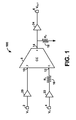
- Figure 1 is a circuit diagram showing an instrumentation amplifier 100 implemented with a single current conveyor 8,
- current conveyor 8 is a type 2 current conveyor (CCII).
- Current conveyor 8 has an x input 12, a y input 10, and a z output 14.
- the voltage at input terminals 10 and 12 is equal, and the current at output terminal 14 is proportional to that of input terminal 12, by a factor of a current gain.
- the current gain may be unity.
- This example comprises two input voltage lines, input voltage line 2 carrying voltage V 1 and input voltage line 4 carrying voltage V 2 , and one output voltage line 6 carrying voltage V OUT .
- Input line 2 may be connected directly to input terminal 10 of current conveyor 8, or may connect through buffer 20, as shown in Figure 1 .
- Input line 4 connects to input terminal 12 through a resistor 16 having resistance R 1 .
- Input line 4 may also connect through buffer 22 and resistor 16, as shown in Figure 1 .
- Output terminal 14 connects to output line 6 and may be connected through buffer 24, as shown in Figure 1 .
- a resistor 18 having resistance R 2 connects output terminal 14 to ground.
- Buffers 20, 22, and 24 may be disposed as shown in Figure 1 to shift the operational frequency range of amplifier 100, or to adjust the impedance or phase delay response of the respective voltage lines, according to the needs and characteristics of the circuit in which instrumentation amplifier 100 sits. Alternatively, any or all of buffers 20, 22, and 24 may be absent from instrumentation amplifier 100.
- buffer 22 may be present in instrumentation amplifier 100 in order to equalize the impedance on input voltage line 4 to that of input voltage line 2.
- each buffer may be an operational amplifier with a non-inverting input, an inverting input, and an output, where the output is fed back to the inverting input, and having a voltage gain of unity.
- buffers having gains greater than unity may be used to reduce noise at the cost of lower CMRR.
- those two buffers may be configured to equalize the phase delay response of the two input voltage lines, or the two buffers may have matched voltage gains.
- Each buffer may also be implemented using a single transistor circuit, such as a source-follower amplifier or an emitter-follower amplifier. Any other suitable buffer or buffer configuration may be used; indeed, a current conveyor may be configured as an appropriate buffer.
- Resistors 16 and 18 may be discrete resistive elements. As an exemplary but not limiting list of possible materials, resistors 16 and 18 may be polysilicon resistors, TaN resistors, CrSi resistors, CrSiN resistors, or SiCCr resistors.
- the resistances of resistors 16 and 18 determine the differential gain of instrumentation amplifier 100, and that differential gain is not contingent upon matching any other pairs of resistors in the circuit.
- the common mode gain of instrumentation amplifier 100 is essentially the common mode gain of current conveyor 8, which is a function of the current conveyor's internal architecture in the same way as it would be for an operational amplifier. Therefore, the CMRR of instrumentation amplifier 100 is limited only by the CMRR of current conveyor 8. Typically, the CMRR of the amplifier is 80 dB to 120 dB or even higher, just like an operational amplifier and presents a significant advantage over prior art instrumentation amplifiers.
- Instrumentation amplifier 100 may present additional advantages. For instance, common mode voltages will not cause unwanted modulation of the voltage on output line 6 when polysilicon resistors are used for R1 and R2, regardless of the differential gain. Further, a differential gain of unity may eliminate distortion in the circuit, even when resistors 16 and 18 are polysilicon resistors. Moreover, the instrumentation amplifier shown in Figure 1 may have a reduced cost over prior art instrumentation amplifiers because of reduced semiconductor area requirements and may require less supply current. The absence of a resistor trim requirement for high CMMR may yield additional cost savings.
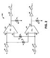
- FIG. 2 is a circuit diagram showing a differential output instrumentation amplifier 200, implemented with two current conveyors 38 and 46, according to an embodiment of the invention.
- current conveyors 38 and 46 are type 2 current conveyors (CCIIs).
- Current conveyor 38 has an x input 42, a y input 40, and a z output 44.
- the voltage at input terminals 40 and 42 is equal, and the current at output terminal 44 is proportional to that of input terminal 42, by a factor of a first current gain.
- Current conveyor 46 has an x input 50, ay input 48, and a z output 52. Again, the voltage at input terminals 50 and 48 is equal, and the current at output terminal 52 is proportional to that of input terminal 50, by a factor of a second current gain.
- the first and second current gains may each be unity.
- This embodiment comprises two input voltage lines, input voltage line 30 carrying voltage V 1 and input voltage line 32 carrying voltage V 2 .
- Input line 30 may be connected directly to input terminal 40 of current conveyor 38, or may connect through buffer 62, as shown in Figure 2 .
- Input line 32 connects to input terminal 42 through a resistor 54 having resistance R 1 .
- a buffer 64 may be inserted before resistor 54 on input line 32.
- Input line 30 connects to input terminal 50 through a resistor 58 having resistance R 3 , and buffer 62 may or may not be inserted upstream of resistor 58.
- input line 32 may be connected directly to input terminal 48 of current conveyor 46, or may connect through buffer 64, as shown in Figure 2 .
- Instrumentation amplifier 200 may also include two output voltage lines, output voltage line 34 carrying voltage V OUT1 and output voltage line 36 carrying voltage V OUT2 .
- Output terminal 44 connects to output line 34 and may be connected through buffer 66, as shown in Figure 2 .
- a resistor 56 having resistance R 2 connects output terminal 44 to ground.
- output terminal 52 connects to output line 36 and may be connected through buffer 68, as shown in Figure 2 .
- a resistor 60 having resistance R 4 connects output terminal 52 to ground.
- buffers 62, 64, 66, and 68 may be disposed as shown in Figure 2 to shift the operational frequency range of amplifier 200, or to adjust the impedance or phase delay response of the respective voltage lines, according to the needs and characteristics of the circuit in which instrumentation amplifier 200 sits.
- any or all of buffers 62, 64, 66, and 68 may be absent from instrumentation amplifier 200.
- each buffer may be an operational amplifier with a non-inverting input, an inverting input, and an output, where the output is fed back to the inverting input, and having a voltage gain of unity.
- buffers having non-unity gains may be used.
- those two buffers may be configured to equalize the phase delay response of the two input voltage lines, or the two buffers may have matched voltage gains.
- Each buffer may also be implemented using a single transistor circuit, such as a source-follower amplifier or an emitter-follower amplifier. Any other suitable buffer, combination of buffers, or buffer configuration may be used; indeed, a current conveyor may be configured as an appropriate buffer.
- Resistors 54, 56, 58, and 60 may be discrete resistive elements.
- resistors 54, 56, 58, and 60 may be polysilicon resistors, TaN resistors, CrSi resistors, CrSiN resistors, or SiCCr resistors.
- the resistances of resistor 54 and resistor 58 may be matched at R 1
- each current conveyor in this circuit depends on its internal architecture and is the same as for the current conveyor shown in Figure 1 ; -80 to -120 dB or lower. Since current conveyor 38 has a positive common-mode gain and current conveyor 46 has a negative common-mode gain, it is possible for this circuit to produce a differential output (V OUT1 - V OUT2 ) that is a function of the common-mode input voltage 1 ⁇ 2 (V 1 + V 2 ). However, if both current conveyors are of the same design, this unwanted differential output will have twice the amplitude of each current conveyor's output. In other words, the magnitude of this common-mode input to differential-mode output conversion will be 6 dB greater than the common-mode response of each current conveyor: - 74 to -114 dB or lower.
- the resistances of resistors 54, 56, 58, and 60 determine the differential gain of instrumentation amplifier 200.
- the CMRR of amplifier 200 may be 74 to 114 dB or more without trim. This presents a significant advantage over prior art differential output instrumentation amplifiers.
- Instrumentation amplifier 200 may present additional advantages. For instance, instrumentation amplifier 200 may have particularly low noise. Further, instrumentation amplifier 200 may have high bandwidth, relative to conventional instrumentation amplifiers implemented using operational amplifiers. Additionally, like instrumentation amplifier 100, this amplifier may have lower trim costs and reduce distortion when used with polysilicon resistors.
Landscapes
- Engineering & Computer Science (AREA)
- Power Engineering (AREA)
- Amplifiers (AREA)
Description
- The disclosure relates to integrated circuits, and, more particularly, to instrumentation amplifiers in integrated circuits.
- Many applications-laboratory, industrial, and audio applications being some examples-share the need to measure the difference between two relatively weak voltages on which there is a common voltage superimposed. Instrumentation amplifiers fill this need by rejecting the superimposed voltage, or common mode voltage, on two input voltages and generating an output voltage that is directly proportional to the difference between the two input voltages. Thus, the output voltage, VOUT, of an instrumentation amplifier is characterized by the operation of a common mode gain, ACM, and a differential gain, ADM, on the two input voltages, V1 and V2, according to the equation:

- An ideal instrumentation amplifier has a constant differential gain and a common mode gain of zero. In practice, the common mode gain may not be zero but instead may be much less than the differential gain. An important measurement for instrumentation amplifiers is the common mode rejection ratio (CMRR), which is a ratio of the common mode gain to the differential gain expressed in decibels. Typical instrumentation amplifiers may have CMRR in the range of 30 to 60 dB, with higher CMRR being desirable.
- Typical instrumentation amplifiers are implemented using operational amplifiers and four or more resistors. The magnitude of resistance presented by particular resistors in the instrumentation amplifier dictates the gain of the amplifier. However, controlling the gain of these amplifiers through resistor selection is typically contingent upon matching paired resistors. Fabrication may be difficult because of the constraint of precisely matching resistor pairs. For example, discrepancies between resistors may be alleviated through the expensive process of resistor trimming.
- Resistors in instrumentation amplifiers may pose additional complications. For instance, resistors, such as polysilicon resistors, may have voltage coefficients that create significant distortion or non-linearity in the output voltage, even when resistor pairs match perfectly. Such voltage coefficients will allow any common mode voltage to effectively modulate the output voltage by changing the differential gain. In the article B. Babaei et al, "High CMRR and Low THD Current Mode Instrumentation Amplifier Using Current Inversion Technique "NORCHIP, 2007, IEEE, Piscataway, NJ, USA, 19 nov. 2007 page 1-4 an instrumentation amplifier using current conveyors is disclosed.
- The present invention in its various aspects is as set out set out in the appended claims.
- In one example, an amplifier using a single current conveyor is disclosed. The current conveyor has an input y, an input x, and an output z, and the current at input x is related to the current at output z by a current gain. Further, the voltage at input x is substantially equal to voltage at input y. A first input voltage line is connected to input y of the current conveyor, and a second input voltage line is connected to input x of the current conveyor through a first resistive element. A second resistive element connects output z of the current conveyor to ground. Additionally, an output voltage line is connected to output z of the current conveyor.
- In an embodiment, an amplifier using two current conveyors is disclosed. The first current conveyor has a first input y, a first input x, and a first output z, and the current at first input x is related to the current at first output z by a first current gain. Additionally, the voltage at first input x is substantially equal to the voltage at first input y. Similarly, the second current conveyor has a second input y, a second input x, and a second output z, and the current at second input x is related to the current at second output z by a second current gain. Again, the voltage at second input x is substantially equal to the voltage at second input y.
- This embodiment contains two input voltage lines and two output voltage lines. The first input voltage line is connected to first input y of the first current conveyor, and the second input voltage line is connected to second input y. Further, the second input voltage line is connected to first input x of the first current conveyor through a first resistive element. A second resistive element connects the first output z of the first current conveyor to ground, and a third resistive element connects the first input voltage line to the second input x. The first output voltage line is connected to first output z of the first current conveyor, and the second output voltage line connected to the second output z of the second current conveyor. Additionally, a fourth resistive element connects the second output z of the second current conveyor to ground.
- Further embodiments include the above amplifiers having buffers on some or all of the input and output voltage lines. These buffers may comprise operational amplifiers and may apply voltage gains and phase delay responses to those voltage lines. The voltage gains may be matched across the input buffers and may equal unity. Additionally, the phase delay response may be matched across the input buffers.
-
-
Figure 1 is a circuit diagram showing an instrumentation amplifier implemented with a single current conveyor, according to an embodiment of the invention. -
Figure 2 is a circuit diagram showing an instrumentation amplifier implemented with two current conveyors, according to another embodiment of the invention. - A current conveyor is a circuit component with two input terminals and one output terminal. The voltage at the two input terminals is equal, and the current at the output terminal is proportional to that of one of the input terminals, by a factor of a current gain. In a current conveyor with a current gain of unity, the current at the output terminal is equal to the current at the appropriate input terminal.
-
Figure 1 is a circuit diagram showing aninstrumentation amplifier 100 implemented with a singlecurrent conveyor 8, In the example,current conveyor 8 is atype 2 current conveyor (CCII).Current conveyor 8 has an x input 12, a yinput 10, and a zoutput 14. As discussed above, the voltage atinput terminals 10 and 12 is equal, and the current atoutput terminal 14 is proportional to that of input terminal 12, by a factor of a current gain. In the example, the current gain may be unity. - This example comprises two input voltage lines,
input voltage line 2 carrying voltage V1 and input voltage line 4 carrying voltage V2, and one output voltage line 6 carrying voltage VOUT. Input line 2 may be connected directly toinput terminal 10 ofcurrent conveyor 8, or may connect throughbuffer 20, as shown inFigure 1 . Input line 4 connects to input terminal 12 through aresistor 16 having resistance R1. Input line 4 may also connect throughbuffer 22 andresistor 16, as shown inFigure 1 .Output terminal 14 connects to output line 6 and may be connected throughbuffer 24, as shown inFigure 1 . Aresistor 18 having resistance R2 connectsoutput terminal 14 to ground. -
Buffers Figure 1 to shift the operational frequency range ofamplifier 100, or to adjust the impedance or phase delay response of the respective voltage lines, according to the needs and characteristics of the circuit in whichinstrumentation amplifier 100 sits. Alternatively, any or all ofbuffers instrumentation amplifier 100. - For example,
buffer 22 may be present ininstrumentation amplifier 100 in order to equalize the impedance on input voltage line 4 to that ofinput voltage line 2. As another example, each buffer may be an operational amplifier with a non-inverting input, an inverting input, and an output, where the output is fed back to the inverting input, and having a voltage gain of unity. - Additionally, buffers having gains greater than unity may be used to reduce noise at the cost of lower CMRR. Further, in an embodiment having two input buffers, those two buffers may be configured to equalize the phase delay response of the two input voltage lines, or the two buffers may have matched voltage gains. Each buffer may also be implemented using a single transistor circuit, such as a source-follower amplifier or an emitter-follower amplifier. Any other suitable buffer or buffer configuration may be used; indeed, a current conveyor may be configured as an appropriate buffer.
-
Resistors resistors - By inspection and using the characteristics of current conveyors described above, the differential gain of
instrumentation amplifier 100 may be calculated as follows:
- Therefore, the resistances of
resistors instrumentation amplifier 100, and that differential gain is not contingent upon matching any other pairs of resistors in the circuit. The common mode gain ofinstrumentation amplifier 100 is essentially the common mode gain ofcurrent conveyor 8, which is a function of the current conveyor's internal architecture in the same way as it would be for an operational amplifier. Therefore, the CMRR ofinstrumentation amplifier 100 is limited only by the CMRR ofcurrent conveyor 8. Typically, the CMRR of the amplifier is 80 dB to 120 dB or even higher, just like an operational amplifier and presents a significant advantage over prior art instrumentation amplifiers. -
Instrumentation amplifier 100 may present additional advantages. For instance, common mode voltages will not cause unwanted modulation of the voltage on output line 6 when polysilicon resistors are used for R1 and R2, regardless of the differential gain. Further, a differential gain of unity may eliminate distortion in the circuit, even whenresistors Figure 1 may have a reduced cost over prior art instrumentation amplifiers because of reduced semiconductor area requirements and may require less supply current. The absence of a resistor trim requirement for high CMMR may yield additional cost savings. -
Figure 2 is a circuit diagram showing a differentialoutput instrumentation amplifier 200, implemented with twocurrent conveyors current conveyors type 2 current conveyors (CCIIs).Current conveyor 38 has anx input 42, a yinput 40, anda z output 44. As discussed above, the voltage atinput terminals output terminal 44 is proportional to that ofinput terminal 42, by a factor of a first current gain.Current conveyor 46 has anx input 50, ayinput 48, anda z output 52. Again, the voltage atinput terminals output terminal 52 is proportional to that ofinput terminal 50, by a factor of a second current gain. In a preferred embodiment, the first and second current gains may each be unity. - This embodiment comprises two input voltage lines,
input voltage line 30 carrying voltage V1 andinput voltage line 32 carrying voltage V2. Input line 30 may be connected directly to inputterminal 40 ofcurrent conveyor 38, or may connect throughbuffer 62, as shown inFigure 2 .Input line 32 connects to input terminal 42 through aresistor 54 having resistance R1. A buffer 64 may be inserted beforeresistor 54 oninput line 32.Input line 30 connects to input terminal 50 through aresistor 58 having resistance R3, and buffer 62 may or may not be inserted upstream ofresistor 58. Finally,input line 32 may be connected directly to inputterminal 48 ofcurrent conveyor 46, or may connect throughbuffer 64, as shown inFigure 2 . -
Instrumentation amplifier 200 may also include two output voltage lines,output voltage line 34 carrying voltage VOUT1 andoutput voltage line 36 carrying voltage VOUT2. Output terminal 44 connects tooutput line 34 and may be connected throughbuffer 66, as shown inFigure 2 . Aresistor 56 having resistance R2 connectsoutput terminal 44 to ground. Further,output terminal 52 connects tooutput line 36 and may be connected throughbuffer 68, as shown inFigure 2 . Aresistor 60 having resistance R4 connectsoutput terminal 52 to ground. - Similarly to the optional buffers of
instrumentation amplifier 100, buffers 62, 64, 66, and 68 may be disposed as shown inFigure 2 to shift the operational frequency range ofamplifier 200, or to adjust the impedance or phase delay response of the respective voltage lines, according to the needs and characteristics of the circuit in whichinstrumentation amplifier 200 sits. Alternatively, any or all ofbuffers instrumentation amplifier 200. - As an example of possible buffer configurations, each buffer may be an operational amplifier with a non-inverting input, an inverting input, and an output, where the output is fed back to the inverting input, and having a voltage gain of unity. Additionally, buffers having non-unity gains may be used. Further, in an embodiment having two input buffers, those two buffers may be configured to equalize the phase delay response of the two input voltage lines, or the two buffers may have matched voltage gains. Each buffer may also be implemented using a single transistor circuit, such as a source-follower amplifier or an emitter-follower amplifier. Any other suitable buffer, combination of buffers, or buffer configuration may be used; indeed, a current conveyor may be configured as an appropriate buffer.
-
Resistors resistors - By inspection and using the characteristics of current conveyors described above, the differential gain of
instrumentation amplifier 200 may be calculated as follows:
resistor 54 andresistor 58 may be matched at R1, and the resistances ofresistor 56 andresistor 60 may be matched at R2, so that the formula for differential gain simplifies to:
- The common-mode gain of each current conveyor in this circuit depends on its internal architecture and is the same as for the current conveyor shown in
Figure 1 ; -80 to -120 dB or lower. Sincecurrent conveyor 38 has a positive common-mode gain andcurrent conveyor 46 has a negative common-mode gain, it is possible for this circuit to produce a differential output (VOUT1 - VOUT2) that is a function of the common-mode input voltage ½ (V1 + V2). However, if both current conveyors are of the same design, this unwanted differential output will have twice the amplitude of each current conveyor's output. In other words, the magnitude of this common-mode input to differential-mode output conversion will be 6 dB greater than the common-mode response of each current conveyor: - 74 to -114 dB or lower. - Therefore, the resistances of
resistors instrumentation amplifier 200. The CMRR ofamplifier 200 may be 74 to 114 dB or more without trim. This presents a significant advantage over prior art differential output instrumentation amplifiers. -
Instrumentation amplifier 200 may present additional advantages. For instance,instrumentation amplifier 200 may have particularly low noise. Further,instrumentation amplifier 200 may have high bandwidth, relative to conventional instrumentation amplifiers implemented using operational amplifiers. Additionally, likeinstrumentation amplifier 100, this amplifier may have lower trim costs and reduce distortion when used with polysilicon resistors. - As in most circuits, those skilled in the art will appreciate that many of the elements described herein are functional entities that may be implemented as discrete components or in conjunction with other components, in any suitable combination and location.
Claims (10)
- An amplifier comprising:a first current conveyer (38) having a first input y (40), a first input x (42), and a first output z (44), wherein current at the first input x is related to current at the first output z by a first current gain, and wherein voltage at the first input x is substantially equal to voltage at the first input y;a first input voltage line (341) connected to the first input y of the first current conveyor;a second input voltage line (32) connected to the first input x of the first current conveyor through a first resistive element (54);a second resistive element (56) connecting the first output z of the current conveyor to ground;a first output voltage line (34) connected to the first output z of the first current conveyor;a second current conveyor (46) having a second input y (48), a second input x (50), and a second output z (52), wherein current at the second input x is related to current at the second output z by a second current gain, wherein voltage at the second input x is substantially equal to the voltage at the second input y, wherein the second input voltage line is connected to second input y, and wherein a third resistive element (58) connects the first input voltage line to the second input x;a second output voltage line (36) connected to the second output z of the second current conveyor; anda fourth resistive element (64) connecting the second output z of the second current conveyor to ground.
- The amplifier of claim 1, further comprising a first input buffer (64) having a non-inverting input and an output, wherein the second input voltage line is connected to the non-inverting input, wherein the output of the first input buffer is connected to the first input x (42) of the first current conveyor through the first resistive element (54), wherein the output of the first input buffer is connected to the second input y (48) of the second current conveyor, and wherein the first input buffer has a first voltage gain.
- The amplifier of claim 2, further comprising a second input buffer (62) having a non-inverting input and an output, wherein the first input voltage line is connected to the non-inverting input, wherein the output of the second input buffer is connected to the first input y (40) of the first current conveyor, wherein the output of the second input buffer is connected to the second input x (50) of the second current conveyor through the third resistive element (58), and wherein the second input buffer has a second voltage gain.
- The amplifier of claim 3, wherein the first voltage gain is equal to the second voltage gain.
- The amplifier of claim 4, wherein the first voltage gain is unity and the second voltage gain is unity.
- The amplifier of claim 3, wherein the first input buffer (64) has a phase delay response equal to a phase delay response of the second input buffer (62).
- The amplifier of claim 1, wherein voltage relationships between the first and the second input voltage lines and the first and second output voltage lines are characterized by a common mode gain and a differential mode gain, wherein a common mode rejection ration (CMRR) is a ratio of the differential mode gain to the common mode gain, and wherein the CMRR is at least 60 dB.
- The amplifier of claim 1, wherein the first resistive element, the second resistive element, the third resistive element (58), and the fourth resistive element (60) each comprises a discrete resistive element, wherein the first resistive element (54) is not matched to the second resistive element, wherein the third resistive element (58) is not matched to the fourth resistive element (60), and wherein the second resistive element is matched to the fourth resistive element.
- The amplifier of claim 1, further comprising:a first output buffer (66) having a non-inverting input and an output, wherein the first output z of the first current conveyor is connected to the non-inverting input of the first output buffer (66), wherein the output of the first output buffer is connected to the first output voltage line, and wherein the first output buffer has a first output buffer voltage gain; anda second output buffer (68) having a non-inverting input and an output,
wherein the second output z of the second current conveyor is connected to the non-inverting input, wherein the output of the second output buffer is connected to the second output voltage line, and wherein the second output buffer has a second output buffer voltage gain. - The amplifier of claim 9, wherein the first output buffer and the second output buffer each comprises an operational amplifier and the first output buffer voltage gain and the second output buffer voltage gain is unity.
Applications Claiming Priority (1)
| Application Number | Priority Date | Filing Date | Title |
|---|---|---|---|
| US12/406,424 US7893759B1 (en) | 2009-03-18 | 2009-03-18 | Current conveyor based instrumentation amplifier |
Publications (2)
| Publication Number | Publication Date |
|---|---|
| EP2230761A1 EP2230761A1 (en) | 2010-09-22 |
| EP2230761B1 true EP2230761B1 (en) | 2012-05-16 |
Family
ID=41728458
Family Applications (1)
| Application Number | Title | Priority Date | Filing Date |
|---|---|---|---|
| EP10150384A Active EP2230761B1 (en) | 2009-03-18 | 2010-01-08 | Current conveyor based instrumentation amplifier |
Country Status (3)
| Country | Link |
|---|---|
| US (1) | US7893759B1 (en) |
| EP (1) | EP2230761B1 (en) |
| JP (1) | JP2010220195A (en) |
Families Citing this family (5)
| Publication number | Priority date | Publication date | Assignee | Title |
|---|---|---|---|---|
| US8081030B2 (en) * | 2008-12-19 | 2011-12-20 | Honeywell International Inc. | Multi-mode amplifier |
| US8519785B2 (en) * | 2011-02-15 | 2013-08-27 | Cavium, Inc. | Differential amplifier with duty cycle compensation |
| US8823450B2 (en) | 2012-07-19 | 2014-09-02 | Honeywell International Inc. | Multiple-output transconductance amplifier based instrumentation amplifier |
| KR101360648B1 (en) | 2012-11-06 | 2014-02-10 | 청주대학교 산학협력단 | Instrumentation amplifier using second generation current-conveyer |
| US9112462B2 (en) | 2013-05-15 | 2015-08-18 | Honeywell International Inc. | Variable-gain dual-output transconductance amplifier-based instrumentation amplifiers |
Family Cites Families (16)
| Publication number | Priority date | Publication date | Assignee | Title |
|---|---|---|---|---|
| GB1496782A (en) | 1974-02-20 | 1978-01-05 | Hamilton T | Generalized current amplifier |
| NL9000518A (en) | 1990-03-07 | 1991-10-01 | Philips Nv | BROADBAND SIGNAL AMPLIFIER. |
| JPH0415887A (en) * | 1990-05-09 | 1992-01-21 | Mitsubishi Electric Corp | Operational amplifier circuit |
| FR2712127B1 (en) | 1993-11-02 | 1995-12-01 | Alcatel Radiotelephone | Amplification element with differential structure in current mode. |
| US6583671B2 (en) | 2000-12-01 | 2003-06-24 | Sony Corporation | Stable AGC transimpedance amplifier with expanded dynamic range |
| US6538503B2 (en) * | 2001-02-22 | 2003-03-25 | Texas Instruments Incorporated | Instrumentation amplifier and method for obtaining high common mode rejection |
| US6710655B2 (en) | 2001-05-23 | 2004-03-23 | Texas Instruments Incorporated | Bipolar emitter couple pair transconductor for high speed operational amplifiers |
| JP3880345B2 (en) * | 2001-08-27 | 2007-02-14 | キヤノン株式会社 | Differential amplifier circuit, solid-state imaging device using the same, and imaging system |
| US6842067B2 (en) | 2002-04-30 | 2005-01-11 | Skyworks Solutions, Inc. | Integrated bias reference |
| US6847569B2 (en) | 2002-12-30 | 2005-01-25 | Intel Corporation | Differential current sense amplifier |
| KR20030053492A (en) | 2003-06-05 | 2003-06-28 | 차형우 | Universal instrumentation amplifier |
| DE602005025760D1 (en) * | 2004-06-15 | 2011-02-17 | Analog Devices Inc | CHOPPER-STABILIZED PRECISION CURRENT MIRROR |
| US7215197B2 (en) | 2004-08-17 | 2007-05-08 | National Instruments Corporation | Programmable gain instrumentation amplifier with improved gain multiplexers |
| JP2006262103A (en) * | 2005-03-17 | 2006-09-28 | Fuji Electric Holdings Co Ltd | Volt-ampere converting circuit and error amplifying circuit |
| JP2006295374A (en) * | 2005-04-07 | 2006-10-26 | Sony Corp | Amplifier circuit, voltage current conversion circuit, and transmitting apparatus |
| US20070057721A1 (en) | 2005-08-31 | 2007-03-15 | Texas Instruments Incorporated | System for amplifiers with low distortion and low output impedance |
-
2009
- 2009-03-18 US US12/406,424 patent/US7893759B1/en active Active
-
2010
- 2010-01-08 EP EP10150384A patent/EP2230761B1/en active Active
- 2010-01-14 JP JP2010006020A patent/JP2010220195A/en active Pending
Also Published As
| Publication number | Publication date |
|---|---|
| US7893759B1 (en) | 2011-02-22 |
| EP2230761A1 (en) | 2010-09-22 |
| JP2010220195A (en) | 2010-09-30 |
Similar Documents
| Publication | Publication Date | Title |
|---|---|---|
| US7911244B2 (en) | Differential drive circuit and communication device | |
| US8854125B2 (en) | Linear amplifier that perform level shift and method of level shifting | |
| US8390378B2 (en) | Method and apparatus for broadband input matching with noise and non-linearity cancellation in power amplifiers | |
| US20120139638A1 (en) | Methods and Circuits for Controlling Amplifier Gain Over Process, Voltage, and Temperature | |
| EP2230761B1 (en) | Current conveyor based instrumentation amplifier | |
| US6313704B1 (en) | Multi-stage signal amplifying circuit | |
| US9685914B2 (en) | Amplifier circuit | |
| US6642741B2 (en) | Electronically adjustable integrated circuit input/output termination method and apparatus | |
| US6160446A (en) | Balanced differential amplifier without common-mode feedback circuit | |
| US8169263B2 (en) | Differential gm-boosting circuit and applications | |
| US7123080B2 (en) | Differential amplification input circuit | |
| EP2688203B1 (en) | Multiple-output transconductance amplifier based instrumentation amplifier | |
| US20120286870A1 (en) | Integrated circuit of an integrator with enhanced stability and related stabilization method | |
| JP2020148699A (en) | Semiconductor device | |
| US7701284B2 (en) | Line driver capable of automatically adjusting output impedance | |
| WO2011047159A1 (en) | High speed intra-pair de-skew circuit | |
| US7127061B2 (en) | Line driver for digital signal transmission | |
| JP4839572B2 (en) | Input circuit | |
| US5394113A (en) | High impedance low-distortion linear amplifier | |
| US8692617B2 (en) | Balanced-input current-sensing differential amplifier | |
| JP3460932B2 (en) | Absolute value circuit | |
| US20230095506A1 (en) | Amplifier circuit, differential amplifier circuit, reception circuit, and semiconductor integrated circuit | |
| US7816971B2 (en) | Switch circuit having adjustable linearity of differential mode resistances | |
| US7812668B2 (en) | Multi-input operational amplifier and method for reducing input offset thereof | |
| JP6053997B1 (en) | Filter device |
Legal Events
| Date | Code | Title | Description |
|---|---|---|---|
| PUAI | Public reference made under article 153(3) epc to a published international application that has entered the european phase |
Free format text: ORIGINAL CODE: 0009012 |
|
| 17P | Request for examination filed |
Effective date: 20100108 |
|
| AK | Designated contracting states |
Kind code of ref document: A1 Designated state(s): AT BE BG CH CY CZ DE DK EE ES FI FR GB GR HR HU IE IS IT LI LT LU LV MC MK MT NL NO PL PT RO SE SI SK SM TR |
|
| AX | Request for extension of the european patent |
Extension state: AL BA RS |
|
| GRAP | Despatch of communication of intention to grant a patent |
Free format text: ORIGINAL CODE: EPIDOSNIGR1 |
|
| GRAS | Grant fee paid |
Free format text: ORIGINAL CODE: EPIDOSNIGR3 |
|
| GRAA | (expected) grant |
Free format text: ORIGINAL CODE: 0009210 |
|
| AK | Designated contracting states |
Kind code of ref document: B1 Designated state(s): AT BE BG CH CY CZ DE DK EE ES FI FR GB GR HR HU IE IS IT LI LT LU LV MC MK MT NL NO PL PT RO SE SI SK SM TR |
|
| REG | Reference to a national code |
Ref country code: GB Ref legal event code: FG4D |
|
| REG | Reference to a national code |
Ref country code: CH Ref legal event code: EP |
|
| REG | Reference to a national code |
Ref country code: AT Ref legal event code: REF Ref document number: 558494 Country of ref document: AT Kind code of ref document: T Effective date: 20120615 |
|
| REG | Reference to a national code |
Ref country code: IE Ref legal event code: FG4D |
|
| REG | Reference to a national code |
Ref country code: DE Ref legal event code: R096 Ref document number: 602010001544 Country of ref document: DE Effective date: 20120719 |
|
| REG | Reference to a national code |
Ref country code: NL Ref legal event code: VDEP Effective date: 20120516 |
|
| REG | Reference to a national code |
Ref country code: LT Ref legal event code: MG4D Effective date: 20120516 |
|
| PG25 | Lapsed in a contracting state [announced via postgrant information from national office to epo] |
Ref country code: FI Free format text: LAPSE BECAUSE OF FAILURE TO SUBMIT A TRANSLATION OF THE DESCRIPTION OR TO PAY THE FEE WITHIN THE PRESCRIBED TIME-LIMIT Effective date: 20120516 Ref country code: CY Free format text: LAPSE BECAUSE OF FAILURE TO SUBMIT A TRANSLATION OF THE DESCRIPTION OR TO PAY THE FEE WITHIN THE PRESCRIBED TIME-LIMIT Effective date: 20120516 Ref country code: PL Free format text: LAPSE BECAUSE OF FAILURE TO SUBMIT A TRANSLATION OF THE DESCRIPTION OR TO PAY THE FEE WITHIN THE PRESCRIBED TIME-LIMIT Effective date: 20120516 Ref country code: LT Free format text: LAPSE BECAUSE OF FAILURE TO SUBMIT A TRANSLATION OF THE DESCRIPTION OR TO PAY THE FEE WITHIN THE PRESCRIBED TIME-LIMIT Effective date: 20120516 Ref country code: IS Free format text: LAPSE BECAUSE OF FAILURE TO SUBMIT A TRANSLATION OF THE DESCRIPTION OR TO PAY THE FEE WITHIN THE PRESCRIBED TIME-LIMIT Effective date: 20120916 Ref country code: SE Free format text: LAPSE BECAUSE OF FAILURE TO SUBMIT A TRANSLATION OF THE DESCRIPTION OR TO PAY THE FEE WITHIN THE PRESCRIBED TIME-LIMIT Effective date: 20120516 Ref country code: NO Free format text: LAPSE BECAUSE OF FAILURE TO SUBMIT A TRANSLATION OF THE DESCRIPTION OR TO PAY THE FEE WITHIN THE PRESCRIBED TIME-LIMIT Effective date: 20120816 |
|
| REG | Reference to a national code |
Ref country code: AT Ref legal event code: MK05 Ref document number: 558494 Country of ref document: AT Kind code of ref document: T Effective date: 20120516 |
|
| PG25 | Lapsed in a contracting state [announced via postgrant information from national office to epo] |
Ref country code: PT Free format text: LAPSE BECAUSE OF FAILURE TO SUBMIT A TRANSLATION OF THE DESCRIPTION OR TO PAY THE FEE WITHIN THE PRESCRIBED TIME-LIMIT Effective date: 20120917 Ref country code: GR Free format text: LAPSE BECAUSE OF FAILURE TO SUBMIT A TRANSLATION OF THE DESCRIPTION OR TO PAY THE FEE WITHIN THE PRESCRIBED TIME-LIMIT Effective date: 20120817 Ref country code: SI Free format text: LAPSE BECAUSE OF FAILURE TO SUBMIT A TRANSLATION OF THE DESCRIPTION OR TO PAY THE FEE WITHIN THE PRESCRIBED TIME-LIMIT Effective date: 20120516 Ref country code: LV Free format text: LAPSE BECAUSE OF FAILURE TO SUBMIT A TRANSLATION OF THE DESCRIPTION OR TO PAY THE FEE WITHIN THE PRESCRIBED TIME-LIMIT Effective date: 20120516 Ref country code: HR Free format text: LAPSE BECAUSE OF FAILURE TO SUBMIT A TRANSLATION OF THE DESCRIPTION OR TO PAY THE FEE WITHIN THE PRESCRIBED TIME-LIMIT Effective date: 20120516 |
|
| PG25 | Lapsed in a contracting state [announced via postgrant information from national office to epo] |
Ref country code: BE Free format text: LAPSE BECAUSE OF FAILURE TO SUBMIT A TRANSLATION OF THE DESCRIPTION OR TO PAY THE FEE WITHIN THE PRESCRIBED TIME-LIMIT Effective date: 20120516 |
|
| PG25 | Lapsed in a contracting state [announced via postgrant information from national office to epo] |
Ref country code: RO Free format text: LAPSE BECAUSE OF FAILURE TO SUBMIT A TRANSLATION OF THE DESCRIPTION OR TO PAY THE FEE WITHIN THE PRESCRIBED TIME-LIMIT Effective date: 20120516 Ref country code: EE Free format text: LAPSE BECAUSE OF FAILURE TO SUBMIT A TRANSLATION OF THE DESCRIPTION OR TO PAY THE FEE WITHIN THE PRESCRIBED TIME-LIMIT Effective date: 20120516 Ref country code: CZ Free format text: LAPSE BECAUSE OF FAILURE TO SUBMIT A TRANSLATION OF THE DESCRIPTION OR TO PAY THE FEE WITHIN THE PRESCRIBED TIME-LIMIT Effective date: 20120516 Ref country code: SK Free format text: LAPSE BECAUSE OF FAILURE TO SUBMIT A TRANSLATION OF THE DESCRIPTION OR TO PAY THE FEE WITHIN THE PRESCRIBED TIME-LIMIT Effective date: 20120516 Ref country code: NL Free format text: LAPSE BECAUSE OF FAILURE TO SUBMIT A TRANSLATION OF THE DESCRIPTION OR TO PAY THE FEE WITHIN THE PRESCRIBED TIME-LIMIT Effective date: 20120516 Ref country code: AT Free format text: LAPSE BECAUSE OF FAILURE TO SUBMIT A TRANSLATION OF THE DESCRIPTION OR TO PAY THE FEE WITHIN THE PRESCRIBED TIME-LIMIT Effective date: 20120516 Ref country code: DK Free format text: LAPSE BECAUSE OF FAILURE TO SUBMIT A TRANSLATION OF THE DESCRIPTION OR TO PAY THE FEE WITHIN THE PRESCRIBED TIME-LIMIT Effective date: 20120516 |
|
| PG25 | Lapsed in a contracting state [announced via postgrant information from national office to epo] |
Ref country code: IT Free format text: LAPSE BECAUSE OF FAILURE TO SUBMIT A TRANSLATION OF THE DESCRIPTION OR TO PAY THE FEE WITHIN THE PRESCRIBED TIME-LIMIT Effective date: 20120516 |
|
| PLBE | No opposition filed within time limit |
Free format text: ORIGINAL CODE: 0009261 |
|
| STAA | Information on the status of an ep patent application or granted ep patent |
Free format text: STATUS: NO OPPOSITION FILED WITHIN TIME LIMIT |
|
| 26N | No opposition filed |
Effective date: 20130219 |
|
| PG25 | Lapsed in a contracting state [announced via postgrant information from national office to epo] |
Ref country code: ES Free format text: LAPSE BECAUSE OF FAILURE TO SUBMIT A TRANSLATION OF THE DESCRIPTION OR TO PAY THE FEE WITHIN THE PRESCRIBED TIME-LIMIT Effective date: 20120827 |
|
| REG | Reference to a national code |
Ref country code: DE Ref legal event code: R097 Ref document number: 602010001544 Country of ref document: DE Effective date: 20130219 |
|
| PG25 | Lapsed in a contracting state [announced via postgrant information from national office to epo] |
Ref country code: BG Free format text: LAPSE BECAUSE OF FAILURE TO SUBMIT A TRANSLATION OF THE DESCRIPTION OR TO PAY THE FEE WITHIN THE PRESCRIBED TIME-LIMIT Effective date: 20120816 |
|
| PG25 | Lapsed in a contracting state [announced via postgrant information from national office to epo] |
Ref country code: MC Free format text: LAPSE BECAUSE OF NON-PAYMENT OF DUE FEES Effective date: 20130131 |
|
| REG | Reference to a national code |
Ref country code: IE Ref legal event code: MM4A |
|
| PG25 | Lapsed in a contracting state [announced via postgrant information from national office to epo] |
Ref country code: IE Free format text: LAPSE BECAUSE OF NON-PAYMENT OF DUE FEES Effective date: 20130108 |
|
| PG25 | Lapsed in a contracting state [announced via postgrant information from national office to epo] |
Ref country code: MT Free format text: LAPSE BECAUSE OF FAILURE TO SUBMIT A TRANSLATION OF THE DESCRIPTION OR TO PAY THE FEE WITHIN THE PRESCRIBED TIME-LIMIT Effective date: 20120516 |
|
| REG | Reference to a national code |
Ref country code: CH Ref legal event code: PL |
|
| PG25 | Lapsed in a contracting state [announced via postgrant information from national office to epo] |
Ref country code: CH Free format text: LAPSE BECAUSE OF NON-PAYMENT OF DUE FEES Effective date: 20140131 Ref country code: LI Free format text: LAPSE BECAUSE OF NON-PAYMENT OF DUE FEES Effective date: 20140131 |
|
| PG25 | Lapsed in a contracting state [announced via postgrant information from national office to epo] |
Ref country code: SM Free format text: LAPSE BECAUSE OF FAILURE TO SUBMIT A TRANSLATION OF THE DESCRIPTION OR TO PAY THE FEE WITHIN THE PRESCRIBED TIME-LIMIT Effective date: 20120516 |
|
| PG25 | Lapsed in a contracting state [announced via postgrant information from national office to epo] |
Ref country code: TR Free format text: LAPSE BECAUSE OF FAILURE TO SUBMIT A TRANSLATION OF THE DESCRIPTION OR TO PAY THE FEE WITHIN THE PRESCRIBED TIME-LIMIT Effective date: 20120516 |
|
| PG25 | Lapsed in a contracting state [announced via postgrant information from national office to epo] |
Ref country code: LU Free format text: LAPSE BECAUSE OF NON-PAYMENT OF DUE FEES Effective date: 20130108 Ref country code: HU Free format text: LAPSE BECAUSE OF FAILURE TO SUBMIT A TRANSLATION OF THE DESCRIPTION OR TO PAY THE FEE WITHIN THE PRESCRIBED TIME-LIMIT; INVALID AB INITIO Effective date: 20100108 Ref country code: MK Free format text: LAPSE BECAUSE OF FAILURE TO SUBMIT A TRANSLATION OF THE DESCRIPTION OR TO PAY THE FEE WITHIN THE PRESCRIBED TIME-LIMIT Effective date: 20120516 |
|
| REG | Reference to a national code |
Ref country code: FR Ref legal event code: PLFP Year of fee payment: 7 |
|
| REG | Reference to a national code |
Ref country code: FR Ref legal event code: PLFP Year of fee payment: 8 |
|
| REG | Reference to a national code |
Ref country code: FR Ref legal event code: PLFP Year of fee payment: 9 |
|
| PGFP | Annual fee paid to national office [announced via postgrant information from national office to epo] |
Ref country code: FR Payment date: 20230124 Year of fee payment: 14 |
|
| P01 | Opt-out of the competence of the unified patent court (upc) registered |
Effective date: 20230525 |
|
| PGFP | Annual fee paid to national office [announced via postgrant information from national office to epo] |
Ref country code: DE Payment date: 20240129 Year of fee payment: 15 Ref country code: GB Payment date: 20240123 Year of fee payment: 15 |