EP2160927B1 - Circuit arrangement and method for controlling light-emitting components - Google Patents
Circuit arrangement and method for controlling light-emitting components Download PDFInfo
- Publication number
- EP2160927B1 EP2160927B1 EP08761220.6A EP08761220A EP2160927B1 EP 2160927 B1 EP2160927 B1 EP 2160927B1 EP 08761220 A EP08761220 A EP 08761220A EP 2160927 B1 EP2160927 B1 EP 2160927B1
- Authority
- EP
- European Patent Office
- Prior art keywords
- light
- voltage
- switching
- emitting component
- supply
- Prior art date
- Legal status (The legal status is an assumption and is not a legal conclusion. Google has not performed a legal analysis and makes no representation as to the accuracy of the status listed.)
- Active
Links
- 238000000034 method Methods 0.000 title claims description 10
- 239000003990 capacitor Substances 0.000 claims description 13
- 230000001276 controlling effect Effects 0.000 claims description 10
- 239000004065 semiconductor Substances 0.000 claims description 8
- 238000012545 processing Methods 0.000 claims description 7
- 230000008093 supporting effect Effects 0.000 claims description 6
- 238000004891 communication Methods 0.000 claims description 4
- 230000001105 regulatory effect Effects 0.000 claims description 2
- 230000005540 biological transmission Effects 0.000 description 8
- 230000003287 optical effect Effects 0.000 description 7
- 230000000694 effects Effects 0.000 description 6
- 230000003071 parasitic effect Effects 0.000 description 6
- 230000008901 benefit Effects 0.000 description 5
- PNDPGZBMCMUPRI-UHFFFAOYSA-N iodine Chemical compound II PNDPGZBMCMUPRI-UHFFFAOYSA-N 0.000 description 4
- 238000013459 approach Methods 0.000 description 2
- 239000000835 fiber Substances 0.000 description 2
- 239000003365 glass fiber Substances 0.000 description 2
- 230000010355 oscillation Effects 0.000 description 2
- 241001295925 Gegenes Species 0.000 description 1
- 230000003213 activating effect Effects 0.000 description 1
- 238000013461 design Methods 0.000 description 1
- 230000005670 electromagnetic radiation Effects 0.000 description 1
- 230000001939 inductive effect Effects 0.000 description 1
- 230000033001 locomotion Effects 0.000 description 1
- 238000010295 mobile communication Methods 0.000 description 1
- 238000012986 modification Methods 0.000 description 1
- 230000004048 modification Effects 0.000 description 1
- 230000000630 rising effect Effects 0.000 description 1
- 238000000926 separation method Methods 0.000 description 1
- 238000001228 spectrum Methods 0.000 description 1
- 230000003068 static effect Effects 0.000 description 1
Images

Classifications
-
- H—ELECTRICITY
- H05—ELECTRIC TECHNIQUES NOT OTHERWISE PROVIDED FOR
- H05B—ELECTRIC HEATING; ELECTRIC LIGHT SOURCES NOT OTHERWISE PROVIDED FOR; CIRCUIT ARRANGEMENTS FOR ELECTRIC LIGHT SOURCES, IN GENERAL
- H05B47/00—Circuit arrangements for operating light sources in general, i.e. where the type of light source is not relevant
- H05B47/10—Controlling the light source
-
- H—ELECTRICITY
- H01—ELECTRIC ELEMENTS
- H01S—DEVICES USING THE PROCESS OF LIGHT AMPLIFICATION BY STIMULATED EMISSION OF RADIATION [LASER] TO AMPLIFY OR GENERATE LIGHT; DEVICES USING STIMULATED EMISSION OF ELECTROMAGNETIC RADIATION IN WAVE RANGES OTHER THAN OPTICAL
- H01S5/00—Semiconductor lasers
- H01S5/04—Processes or apparatus for excitation, e.g. pumping, e.g. by electron beams
- H01S5/042—Electrical excitation ; Circuits therefor
-
- H—ELECTRICITY
- H01—ELECTRIC ELEMENTS
- H01S—DEVICES USING THE PROCESS OF LIGHT AMPLIFICATION BY STIMULATED EMISSION OF RADIATION [LASER] TO AMPLIFY OR GENERATE LIGHT; DEVICES USING STIMULATED EMISSION OF ELECTROMAGNETIC RADIATION IN WAVE RANGES OTHER THAN OPTICAL
- H01S5/00—Semiconductor lasers
- H01S5/06—Arrangements for controlling the laser output parameters, e.g. by operating on the active medium
- H01S5/062—Arrangements for controlling the laser output parameters, e.g. by operating on the active medium by varying the potential of the electrodes
-
- H—ELECTRICITY
- H05—ELECTRIC TECHNIQUES NOT OTHERWISE PROVIDED FOR
- H05B—ELECTRIC HEATING; ELECTRIC LIGHT SOURCES NOT OTHERWISE PROVIDED FOR; CIRCUIT ARRANGEMENTS FOR ELECTRIC LIGHT SOURCES, IN GENERAL
- H05B45/00—Circuit arrangements for operating light-emitting diodes [LED]
- H05B45/30—Driver circuits
- H05B45/395—Linear regulators
- H05B45/397—Current mirror circuits
-
- Y—GENERAL TAGGING OF NEW TECHNOLOGICAL DEVELOPMENTS; GENERAL TAGGING OF CROSS-SECTIONAL TECHNOLOGIES SPANNING OVER SEVERAL SECTIONS OF THE IPC; TECHNICAL SUBJECTS COVERED BY FORMER USPC CROSS-REFERENCE ART COLLECTIONS [XRACs] AND DIGESTS
- Y02—TECHNOLOGIES OR APPLICATIONS FOR MITIGATION OR ADAPTATION AGAINST CLIMATE CHANGE
- Y02B—CLIMATE CHANGE MITIGATION TECHNOLOGIES RELATED TO BUILDINGS, e.g. HOUSING, HOUSE APPLIANCES OR RELATED END-USER APPLICATIONS
- Y02B20/00—Energy efficient lighting technologies, e.g. halogen lamps or gas discharge lamps
- Y02B20/30—Semiconductor lamps, e.g. solid state lamps [SSL] light emitting diodes [LED] or organic LED [OLED]
Definitions
- the present invention relates generally to the technical field of driving light-emitting components.
- the present invention relates in particular to a circuit arrangement, in particular a driver circuit, and a method for controlling at least one light-emitting component (cf. publication EP 0 798 828 A2 and also block letters US2006 / 133435 A1 ).
- the term light or light-emitting is understood to mean not only the range of electromagnetic radiation visible to the eye, which extends in a wavelength range from about 380 nanometers to about 780 nanometers (which corresponds to a frequency of about 789 terahertz to down to about 385 terahertz).
- the term light or light-emitting is understood to mean the entire electromagnetic wavelength or frequency spectrum that is not visible to the eye, in particular the I [nfra] R [ot] range (wavelength range up to about 2,000 nanometers or frequency range down to about 150 terahertz), for example a wavelength of about 850 nanometers or a frequency of about 350 terahertz.
- a semiconductor laser or a light-emitting diode is used as the light-emitting component E, in particular as an optical transmission element or as an optical source, for optical data transmission.
- this semiconductor laser or this light-emitting diode is driven, for example, by an electronic driver circuit S1 (cf. Figure 5A ), S2 (cf. Figure 5B ) or S3 (cf. Figure 5C ) is supplied with the necessary operating voltage, the bias current and the modulation current for correct operation.
- S1 cf. Figure 5A
- S2 cf. Figure 5B
- S3 cf. Figure 5C
- the light-emitting component E can be supplied with current via a first current path I 1 and additionally via a second current path I 2.
- the current I 1 flows in the first current path from a DC voltage source Q via the light-emitting component E to a constant current source K1 for I 1 .
- a constant current source K2 is provided for supplying power to the second current path I 2.
- the light-emitting component E is thus modulated in the form of current setting or current modulation, that is, by varying the current strengths flowing through the light-emitting component E between the values I 1 and I 1 + I 2 over time .
- the arrangement of changeover switch U and reactive load R has the effect that the same current always flows at the node assigned to the changeover switch U with respect to the second current path I 2 , the current I 2 in the event that the second current path I 2 is not the light-emitting component E is switched on, in the reactive load R is essentially converted into thermal energy, which can be the case, for example, for about fifty percent of the operating time of the light-emitting component; however, the current I 2 is disadvantageously also present when this current I 2 is not needed at all.
- the illustrated second exemplary driver circuit S2 flows when the second current path I 2 is activated or connected by means of the switch U controlling the current level through the light-emitting component E, the current I 1 + I 2 , otherwise the current I 1 ; however, the current I 2 is disadvantageously also present when this current I 2 is not needed at all.
- the illustrated third exemplary driver circuit S3 according to the prior art, depending on the position of the switch U controlling the current level, flows through the light-emitting component E, the current I 1 + 0.5 ⁇ I 2 or the current I 1 -0.5 ⁇ I 2 , that means here too the current difference is I 2 .
- the arrangement of a (not mandatory) coil L, across which a voltage of about 0.5 volts drops, for example, is usually used to increase the impedance of the constant current source K1 at high frequencies and consequently enables the use of a constant current source K1 that does not have a high output impedance at high frequencies .
- driver circuit S3 is also from the publication US 6 667 661 B1
- a driver circuit with a coil is known from the prior art.
- Another small voltage drop of, for example, about 0.1 volts occurs across the switching element U, so that (too) little voltage drops across the light-emitting component and thus (too) little voltage is available at the light-emitting component.
- the present invention is based on the object of further developing a circuit arrangement of the type mentioned and a method of the type mentioned in such a way that the disadvantages and inadequacies set out above are avoided;
- the current requirement and output resistance should be as low as possible, so that the highest possible frequency or switching speed and the highest possible output voltage for the light-emitting component can be achieved.
- the switching element is expediently as at least one on switch or as at least one changeover switch or as at least one changeover switch, for example as at least one switching transistor, such as at least one M [etal] O [xide] S [emiconductor] field] E [ffect ] T [ransistor], trained.
- at least one switching transistor such as at least one M [etal] O [xide] S [emiconductor] field] E [ffect ] T [ransistor], trained.
- a supply element in the sense of the present invention can be implemented, for example, as at least one voltage source or as a combination of current source and backup capacitor, so that a low output impedance is created for the relevant operating frequencies.
- the light-emitting component can thus be controlled by varying its operating voltage by switching the voltage applied to the light-emitting component, in particular the voltage impressed on the light-emitting component, and can be used, for example, for optical data transmission.
- the light-emitting component converts electrical signals into optical signals, which are coupled into an optical waveguide, for example into a glass fiber or into a plastic fiber.
- the light-emitting component is operated voltage-driven in at least two operating points that can be configured by means of the switching element and optionally by means of at least one control device, in particular a signal source, for controlling the switching element.
- the circuit arrangement according to the invention is particularly advantageous because of its low power consumption.
- the current requirement is particularly low because - in contrast to the prior art - there is no further current path outside the light-emitting component.
- the data transmission can take place, for example, via at least one carrier medium, such as glass fiber or plastic fiber, or also via air as the carrier medium or by vacuum.
- carrier medium such as glass fiber or plastic fiber
- the present invention can be used particularly advantageously in a mobile communication device or in a mobile data processing device, because in these areas of application the supply voltage made available by the battery or by the accumulator unit, also known as the accumulator, is limited; In terms of the longest possible operating time for the battery, efficient handling of the supply voltage and power consumption made possible by the present invention is of particular benefit.
- circuit arrangement according to the present invention as well as the method according to the present invention have both a low output impedance and a low energy requirement.
- this circuit 100 has two supply elements operated against a reference potential or reference potential W, in particular against earth potential or ground potential or zero potential, in the form of voltage sources 10 or 10 '(accumulator unit) to supply the circuit arrangement 100 with the first operating voltage U 1 or with a second operating voltage U 2 .
- a reference potential or reference potential W in particular against earth potential or ground potential or zero potential, in the form of voltage sources 10 or 10 '(accumulator unit) to supply the circuit arrangement 100 with the first operating voltage U 1 or with a second operating voltage U 2 .
- the circuit arrangement 100 is also a switching element 30, in particular a changeover switch or toggle switch, for example a switching transistor for each switching position, such as a M [etal] O [xide] S [emiconductor] -F [ield] E [ffect ] T [ransistor], assigned.
- a switching element 30 in particular a changeover switch or toggle switch, for example a switching transistor for each switching position, such as a M [etal] O [xide] S [emiconductor] -F [ield] E [ffect ] T [ransistor], assigned.
- This switching element 30 is designed to control the light-emitting component 20 by means of switching at least between a first switching position and a second switching position.
- the circuit arrangement 100 ′ according to FIG Fig. 2 has as supply elements two current sources 10 or 10 'connected in parallel to one another, the outputs of which are each capacitively supported by means of a backup capacitor 12 or 12'.
- the circuit arrangement 100 ′ has a supply element in the form of a battery.
- the supply element can also be designed as a capacitively supported current source on the output side, for example as a combination or interconnection of current source 10, 10 'and backup capacitor 12, 12' optimized for applications at low frequencies.
- the current source 10 or 10 ' is used for current tracking as required.
- the backup capacitor 12 or 12 ' is used to reduce the impedance of the node N or N' for the range of switching and operating frequencies of the driver circuit 100 '.
- the current source 10 or 10 ' can be dimensioned in such a way that it works as intended even with a very small voltage difference between the supply voltage 14 and the voltage at the node N or N'.
- the light-emitting component 20 is connected to the node N, at which an exemplary voltage of approximately 2.8 volts is applied.
- the light-emitting component 20 is connected to the node N ', at which an exemplary voltage of approximately 2.3 volts is applied.
- the node N or N 'linking the output of the current source 10 or 10' and the first or second switching position of the switching element 30 is supported with high capacitance by the backup capacitor 12 or 12 'and is essentially "not moved” with the signal to be transmitted ", that means constant.
- the circuit arrangement 100 makes it possible according to FIG Fig. 2 illustrated second embodiment a particularly effective use of the supply voltage 14 as well as the possibility of modification for the current strengths 0.5 ⁇ I 1 or 0.5 ⁇ I 2 (-> switching between the Current intensity I 1 at the light-emitting component 20 in the first switching position and the current I 2 at the light-emitting component 20 in the second switching position, provided that both switching positions are activated equally over time).
- the output impedance of the driver circuit 100 ′ can also be very low at high frequencies because this output impedance is limited only by the parasitic resistance of the switching element 30, so that a very high operating frequency or switching speed can be achieved.
- a very high output voltage can be achieved for the light-emitting component 20, because only a very small voltage drop occurs across the switch 30;
- the current source 10, 10 ' is advantageously arranged in the supply path and not in the high-frequency signal path.
- the illustrated third embodiment of a circuit arrangement is connected between the second node N 'and the second switching position of the switching element 30 in a forward direction, in particular towards the second switching position of the switching element 30, polarized diode 30', for example a pn diode or a Schottky diode .
- This diode 30 ' conducts in the forward direction, that is to say towards the switching element 30, and blocks in the reverse direction.
- the diode 30 'takes over the function of the second (, in Fig. 3 right) switch position, namely to lead when the first (, in Fig. 3 left) current path of switch 30 is switched off.
- a possibly non-negligible forward voltage of the forward-polarized diode 30 ' leads to a correspondingly large voltage loss between the voltage at the node N' and that of the light-emitting component 20 available operating voltage.
- Such a control / processing element 22 can - although in Figure 4A not explicitly shown - also in the case of the circuit arrangement 100 ′ ′′ according to the reference Figure 4A illustrated fourth embodiment of the present invention may be provided.
- the present invention can be designed in a variety of ways; In particular, by adding additional components or additional components to the signal and control paths, the present invention can be adapted to specific requirements.
- connection in the context of the present invention also includes connections or types of connection which are made by additionally introduced components or components.
Description
Die vorliegende Erfindung betrifft allgemein das technische Gebiet der Ansteuerung von lichtemittierenden Bauelementen.The present invention relates generally to the technical field of driving light-emitting components.
Die vorliegende Erfindung betrifft im Spezielleren eine Schaltungsanordnung, insbesondere Treiberschaltung, sowie ein Verfahren zum Ansteuern mindestens eines lichtemittierenden Bauelements (vgl. Druckschrift
Im Rahmen der vorliegenden Erfindung wird unter dem Begriff Licht bzw. lichtemittierend nicht nur der für das Auge sichtbare Bereich der elektromagnetischen Strahlung verstanden, der sich in einem Wellenlängenbereich von etwa 380 Nanometer bis etwa 780 Nanometer erstreckt (, was einer Frequenz von etwa 789 Terahertz bis herab zu etwa 385 Terahertz entspricht).In the context of the present invention, the term light or light-emitting is understood to mean not only the range of electromagnetic radiation visible to the eye, which extends in a wavelength range from about 380 nanometers to about 780 nanometers (which corresponds to a frequency of about 789 terahertz to down to about 385 terahertz).
Vielmehr wird unter dem Begriff Licht bzw. lichtemittierend das gesamte, also auch das für das Auge nicht sichtbare elektromagnetische Wellenlängen- bzw. Frequenzspektrum verstanden, insbesondere der I[nfra]R[ot]-Bereich (Wellenlängenbereich bis zu etwa 2.000 Nanometer bzw. Frequenzbereich bis herab zu etwa 150 Terahertz), zum Beispiel eine Wellenlänge von etwa 850 Nanometer bzw. eine Frequenz von etwa 350 Terahertz.Rather, the term light or light-emitting is understood to mean the entire electromagnetic wavelength or frequency spectrum that is not visible to the eye, in particular the I [nfra] R [ot] range (wavelength range up to about 2,000 nanometers or frequency range down to about 150 terahertz), for example a wavelength of about 850 nanometers or a frequency of about 350 terahertz.
Aus dem Stand der Technik bekannte exemplarische Schaltungsanordnungen zur Ansteuerung eines lichtemittierenden Bauelements E zum Zwecke der Datenübertragung vom lichtemittierenden Bauelement E (= sogenannte Quelle) zu einem lichtempfangenden Bauelement (= sogenannte Senke) sind in
Typischerweise wird zur optischen Datenübertragung als lichtemittierendes Bauelement E, insbesondere als optisches Sendeelement oder als optische Quelle, ein Halbleiterlaser oder eine Leuchtdiode benutzt.Typically, a semiconductor laser or a light-emitting diode is used as the light-emitting component E, in particular as an optical transmission element or as an optical source, for optical data transmission.
Dieser Halbleiterlaser oder diese Leuchtdiode wird gemäß dem Stand der Technik beispielsweise von einer elektronischen Treiberschaltung S1 (vgl.
Die Treiberschaltung S1, S2, S3 kann sowohl als eine integrierte Schaltung (oder IC = Integrated Circuit) als auch diskret aus einzelnen Komponenten auf einer Leiterplatte (oder PCB = Printed Circuit Board) aufgebaut sein.The driver circuit S1, S2, S3 can be constructed both as an integrated circuit (or IC = Integrated Circuit) and also discretely from individual components on a printed circuit board (or PCB = Printed Circuit Board).
Beim in
Durch Aktivschalten oder Zuschalten des zweiten Strompfads I2 mittels eines den Strompegel des lichtemittierenden Bauelements E steuernden Umschalters U fließt durch das lichtemittierende Bauelement E der Gesamtstrom Iges = I1 + I2, ansonsten der Strom I1. Zur Stromversorgung des zweiten Strompfads I2 ist eine Konstantstromquelle K2 vorgesehen.By activating or connecting the second current path I 2 by means of a changeover switch U which controls the current level of the light-emitting component E, flows through the light-emitting component E the total current I tot = I 1 + I 2 , otherwise the current I 1 . A constant current source K2 is provided for supplying power to the second current path I 2.
Die Modulation des lichtemittierenden Bauelements E erfolgt also in Form von Stromeinstellung oder Strommodulation, das heißt durch zeitliches Variieren der durch das lichtemittierende Bauelement E fließenden Stromstärken zwischen den Werten I1 und I1 + I2.The light-emitting component E is thus modulated in the form of current setting or current modulation, that is, by varying the current strengths flowing through the light-emitting component E between the values I 1 and I 1 + I 2 over time .
Die Anordnung von Umschalter U und Blindlast R bewirkt, dass am dem Umschalter U in Bezug auf den zweiten Strompfad I2 zugeordneten Knotenpunkt stets der gleiche Strom fließt, wobei der Strom I2 in dem Falle, dass der zweite Strompfad I2 nicht dem lichtemittierenden Bauelement E zugeschaltet ist, in der Blindlast R im Wesentlichen in thermische Energie umgewandelt wird, was beispielsweise zu etwa fünfzig Prozent der Betriebszeit des lichtemittierenden Bauelements der Fall sein kann; allerdings ist der Strom I2 unvorteilhafterweise auch dann vorhanden, wenn dieser Strom I2 gar nicht benötigt wird.The arrangement of changeover switch U and reactive load R has the effect that the same current always flows at the node assigned to the changeover switch U with respect to the second current path I 2 , the current I 2 in the event that the second current path I 2 is not the light-emitting component E is switched on, in the reactive load R is essentially converted into thermal energy, which can be the case, for example, for about fifty percent of the operating time of the light-emitting component; however, the current I 2 is disadvantageously also present when this current I 2 is not needed at all.
Des Weiteren sind beim in
Bei der in
Die Betriebsspannung des lichtemittierenden Bauelements E hängt von der durch die Spannungsquelle Q zur Verfügung gestellten Versorgungsspannung (= zum Beispiel etwa drei Volt) und von der Konstantstromquelle K1 bzw. von den Konstantstromquellen K1, K2 ab.The operating voltage of the light-emitting component E depends on the supply voltage made available by the voltage source Q (= approximately three volts, for example) and on the constant current source K1 or on the constant current sources K1, K2.
Bei der in
Die Anordnung einer (nicht obligatorischen) Spule L, an der beispielsweise eine Spannung von etwa 0,5 Volt abfällt, dient üblicherweise der Impedanzerhöhung der Konstantstromquelle K1 bei hohen Frequenzen und ermöglicht demzufolge den Einsatz einer Konstantstromquelle K1, die keine hohe Ausgangsimpedanz bei hohen Frequenzen aufweist.The arrangement of a (not mandatory) coil L, across which a voltage of about 0.5 volts drops, for example, is usually used to increase the impedance of the constant current source K1 at high frequencies and consequently enables the use of a constant current source K1 that does not have a high output impedance at high frequencies .
Neben der vorbeschriebenen Treiberschaltung S3 ist auch aus der Druckschrift
Unvorteilhafterweise erforderlich ist bei der in
Aufgrund der Anordnung aus Spule L und Kondensator C können des Weiteren unerwünschte elektromagnetische Störeffekte, wie etwa elektromagnetische Schwingungen, auftreten. Mit dem Problem der Vermeidung elektromagnetischer Schwingungen einer Lasertreiberschaltung mit signalverstärkter Datenübertragung befasst sich in diesem Zusammenhang beispielsweise die Druckschrift
Ein weiterer Nachteil konventioneller Schaltungsanordnungen ist deren hoher Spannungsabfall an den, zum lichtemittierenden Bauelement in Reihe liegenden, Bauelementen. Insbesondere für Anwendungen bei denen nur eine kleine Versorgungsspannung zur Verfügung steht, steht dieses im Widerspruch zum Ziel, am lichtemittierenden Bauelement eine möglichst hohe Betriebsspannung bereit zu stellen.Another disadvantage of conventional circuit arrangements is their high voltage drop across the components in series with the light-emitting component. In particular for applications in which only a small supply voltage is available, this contradicts the goal of providing the highest possible operating voltage on the light-emitting component.
Die technische Problemstellung, eine Treiberschaltung zur optischen Datenübertragung mit geringem Leistungsbedarf bereit zu stellen, ist beispielsweise aus den Druckschriften
Zudem haben aus dem Stand der Technik bekannte Schaltungsanordnungen nachteiligerweise hohe Ausgangswiderstände (= Realteile der Ausgangsimpedanzen). Dies begrenzt die Geschwindigkeit, insbesondere für das Einschwingen (oder Settling) der Schaltungsanordnung, denn die maximale Schaltfrequenz f verhält sich im Wesentlichen reziprok proportional zum Produkt aus Gesamtkapazität C und Gesamtwiderstand R am Ausgang der Ansteuer- oder Treiberschaltung, wobei
- die Gesamtkapazität C zum Beispiel im Wesentlichen durch die parasitäre kapazitive Wirkung des lichtemittierenden Bauelements dominiert ist und
- der Gesamtwiderstand R im Wesentlichen durch die Parallelschaltung des Ausgangswiderstands der Treiberschaltung und des Eingangswiderstands des lichtemittierenden Bauelements gegeben ist.
- the total capacitance C, for example, is essentially dominated by the parasitic capacitive effect of the light-emitting component and
- the total resistance R is essentially given by the parallel connection of the output resistance of the driver circuit and the input resistance of the light-emitting component.
Schließlich ist ein weiteres technisches Problem konventioneller Schaltungsanordnungen eine (zu) niedrige Ausgangsspannung am lichtemittierenden Bauelement, denn die Konstantstromquelle(n) benötigt/en eine(n) Spannung(sabfall) von beispielsweise etwa 0,5 Volt (ein geringer Spannungsabfall in Höhe von beispielsweise etwa 0,2 Volt erfolgt auch an der die Versorgungsspannung zur Verfügung stellenden Spannungsquelle, sofern es sich um eine geregelte Spannungsquelle handelt).Finally, another technical problem with conventional circuit arrangements is an (too) low output voltage at the light-emitting component, because the constant current source (s) requires a voltage (drop) of, for example, about 0.5 volts (a small voltage drop of, for example about 0.2 volts is also applied to the voltage source providing the supply voltage, provided it is a regulated voltage source).
Ein weiterer geringer Spannungsabfall in Höhe von beispielsweise etwa 0,1 Volt erfolgt am Schaltelement U, so dass am lichtemittierenden Bauelement (zu) wenig Spannung abfällt und damit am lichtemittierenden Bauelement (zu) wenig Spannung zur Verfügung steht.Another small voltage drop of, for example, about 0.1 volts occurs across the switching element U, so that (too) little voltage drops across the light-emitting component and thus (too) little voltage is available at the light-emitting component.
Ausgehend von den vorstehend dargelegten Nachteilen und Unzulänglichkeiten sowie unter Würdigung des umrissenen Standes der Technik liegt der vorliegenden Erfindung die Aufgabe zugrunde, eine Schaltungsanordnung der eingangs genannten Art sowie ein Verfahren der eingangs genannten Art so weiterzuentwickeln, dass die vorstehend dargelegten Nachteile und Unzulänglichkeiten vermieden werden; insbesondere sollen Strombedarf und Ausgangswiderstand möglichst niedrig sein, so dass eine möglichst hohe Frequenz oder Schaltgeschwindigkeit sowie eine möglichst hohe Ausgangsspannung für das lichtemittierende Bauelement erzielt werden können.On the basis of the disadvantages and inadequacies set out above and taking into account the prior art outlined, the present invention is based on the object of further developing a circuit arrangement of the type mentioned and a method of the type mentioned in such a way that the disadvantages and inadequacies set out above are avoided; In particular, the current requirement and output resistance should be as low as possible, so that the highest possible frequency or switching speed and the highest possible output voltage for the light-emitting component can be achieved.
Diese Aufgabe wird durch eine Schaltungsanordnung mit den im Anspruch 1 angegebenen Merkmalen sowie durch ein Verfahren mit den im Anspruch 5 angegebenen Merkmalen sowie durch eine Verwendung einer Schaltungsanordnung nach Anspruch 1 mit den in Anspruch 7 angegebenen Merkmalen gelöst.This object is achieved by a circuit arrangement having the features specified in
Das lichtemittierende Bauelement wird
- in der ersten Schaltposition des Schaltelements mit einer ersten Betriebsspannung beaufschlagt,
- in der zweiten Schaltposition des Schaltelements mit einer zweiten Betriebsspannung beaufschlagt und
- durch Umschalten zwischen der ersten Betriebsspannung und der zweiten Betriebsspannung angesteuert; insbesondere wird das lichtemittierende Bauelement durch Umschalten zwischen den Schaltpositionen angesteuert, von denen zumindest die erste Schaltposition des Schaltelements und die zweite Schaltposition des Schaltelements für die Betriebsfrequenz niederimpedant sind.
- applied to a first operating voltage in the first switching position of the switching element,
- acted upon in the second switching position of the switching element with a second operating voltage and
- driven by switching between the first operating voltage and the second operating voltage; In particular, the light-emitting component is controlled by switching between the switching positions, of which at least the first switching position of the switching element and the second switching position of the switching element are low-impedance for the operating frequency.
Das Schaltelement ist zweckmäßigerweise als mindestens ein Einschalter oder als mindestens ein Umschalter oder als mindestens ein Wechselschalter, zum Beispiel als mindestens ein Schalttransistor, wie etwa als mindestens ein M[etal]O[xide]S[emiconductor]F[ield]E[ffect]T[ransistor], ausgebildet. Auf diese Weise sind mindestens zwei Betriebszustände der Schaltungsanordnung mit jeweils niedrigen Impedanzen, insbesondere ohne weitere Stromverluste, erzielbar.The switching element is expediently as at least one on switch or as at least one changeover switch or as at least one changeover switch, for example as at least one switching transistor, such as at least one M [etal] O [xide] S [emiconductor] field] E [ffect ] T [ransistor], trained. In this way, at least two operating states of the circuit arrangement, each with low impedances, in particular without further current losses, can be achieved.
Ein Versorgungselement im Sinne der vorliegenden Erfindung kann beispielsweise als mindestens eine Spannungsquelle oder als Kombination aus Stromquelle und Stützkondensator realisiert sein, so dass für die relevanten Betriebsfrequenzen eine niedrige Ausgangsimpedanz entsteht.A supply element in the sense of the present invention can be implemented, for example, as at least one voltage source or as a combination of current source and backup capacitor, so that a low output impedance is created for the relevant operating frequencies.
Das lichtemittierende Bauelement ist somit durch Variieren seiner Betriebsspannung mittels Umschaltens der auf das lichtemittierende Bauelement beaufschlagten Spannung, insbesondere der in das lichtemittierende Bauelement eingeprägten Spannung, ansteuerbar und kann beispielsweise zur optischen Datenübertragung dienen. Hierzu wandelt das lichtemittierende Bauelement elektrische Signale in optische Signale um, die in einen Lichtwellenleiter, beispielsweise in eine Glasfaser oder in eine Kunststofffaser, eingekoppelt werden.The light-emitting component can thus be controlled by varying its operating voltage by switching the voltage applied to the light-emitting component, in particular the voltage impressed on the light-emitting component, and can be used, for example, for optical data transmission. For this purpose, the light-emitting component converts electrical signals into optical signals, which are coupled into an optical waveguide, for example into a glass fiber or into a plastic fiber.
Bei der vorliegenden Erfindung wird das lichtemittierende Bauelement somit spannungsgesteuert ("voltage-driven") in mindestens zwei Arbeitspunkten betrieben, die mittels des Schaltelements sowie optionalerweise mittels mindestens einer Steuerungseinrichtung, insbesondere Signalquelle, zum Steuern des Schaltelements konfigurierbar sind.In the present invention, the light-emitting component is operated voltage-driven in at least two operating points that can be configured by means of the switching element and optionally by means of at least one control device, in particular a signal source, for controlling the switching element.
Die erfindungsgemäße Schaltungsanordnung ist aufgrund ihres niedrigen Strombedarfs besonders vorteilhaft. Der Strombedarf ist besonders niedrig, weil es - im Unterschied zum Stand der Technik - außerhalb des lichtemittierenden Bauelements keinen weiteren Strompfad gibt.The circuit arrangement according to the invention is particularly advantageous because of its low power consumption. The current requirement is particularly low because - in contrast to the prior art - there is no further current path outside the light-emitting component.
Des Weiteren wird der Fachmann bei der vorliegenden Erfindung die vergleichsweise hohe, für das lichtemittierende Bauelement zur Verfügung stehende Ausgangsspannung besonders zu schätzen wissen.Furthermore, with the present invention, those skilled in the art will particularly appreciate the comparatively high output voltage available for the light-emitting component.
Ferner ist die niedrige Ausgangsimpedanz ein weiterer Vorteil der vorliegenden Erfindung. Dies ermöglicht eine hohe Geschwindigkeit, insbesondere für das Einschwingen der Schaltungsanordnung, denn die maximale Schaltfrequenz f verhält sich im Wesentlichen reziprok proportional zum Produkt aus Gesamtkapazität C und Gesamtwiderstand R am Ausgang der Ansteuer- oder Treiberschaltung, wobei
- die Gesamtkapazität C zum Beispiel im Wesentlichen durch die parasitäre kapazitive Wirkung des lichtemittierenden Bauelements dominiert ist und
- der Gesamtwiderstand R im Wesentlichen durch die Parallelschaltung des Ausgangswiderstands der Treiberschaltung und des Eingangswiderstands des lichtemittierenden Bauelements gegeben ist.
- the total capacitance C, for example, is essentially dominated by the parasitic capacitive effect of the light-emitting component and
- the total resistance R is essentially given by the parallel connection of the output resistance of the driver circuit and the input resistance of the light-emitting component.
Beim lichtemittierenden Bauelement handelt es sich um eine lichtemittierende Diode (= L[ight]E[mitting]D[iode]), wie etwa um eine Leuchtdiode, oder etwa um einen Halbleiterlaser.The light-emitting component is a light-emitting diode (= L [ight] E [mitting] D [iode]), such as a light-emitting diode or a semiconductor laser.
Das Ansteuern des lichtemittierenden Bauelements erfolgt zum Beispiel zum Zwecke der Datenübertragung von mindestens einem lichtemittierenden Bauelement (= sogenannte Quelle) zu mindestens einem lichtempfangenden Bauelement (= sogenannte Senke).The light-emitting component is controlled, for example, for the purpose of data transmission from at least one light-emitting component (= so-called source) to at least one light-receiving component (= so-called sink).
Die Datenübertragung kann zum Beispiel über mindestens ein Trägermedium, wie etwa über Glasfaser oder über Kunststofffaser, oder auch über Luft als Trägermedium oder durch Vakuum erfolgen.The data transmission can take place, for example, via at least one carrier medium, such as glass fiber or plastic fiber, or also via air as the carrier medium or by vacuum.
Die vorliegende Erfindung betrifft schließlich die Verwendung mindestens einer Schaltungsanordnung, insbesondere mindestens einer Treiberschaltung, gemäß der vorstehend dargelegten Art und/oder eines Verfahrens gemäß der vorstehend dargelegten Art
- in mindestens einer, insbesondere mobilen, Telekommunikationsanlage, zum Beispiel in mindestens einem Kommunikationsgerät, wie etwa in mindestens einem Mobiltelefon,
- in mindestens einer, insbesondere mobilen, Datenkommunikationsanlage oder in mindestens einer, insbesondere mobilen, Datenverarbeitungseinrichtung, zum Beispiel in mindestens einem Handheld, in mindestens einem Notebook oder in mindestens einem P[ersonal]D[igital]A[ssistant],
- in mindestens einer, insbesondere mobilen, Datenaufzeichnungs- und/oder -wiedergabeeinrichtung, zum Beispiel in mindestens einem Camcorder, in mindestens einer Digitalkamera oder in mindestens einem H[igh]D[efinition]T[ele]V[ision], oder
- in mindestens einem Fortbewegungsmittel, zum Beispiel in mindestens einem Fahrerassistenzsystem oder in mindestens einem Navigationssystem eines Automobils.
- in at least one, in particular mobile, telecommunication system, for example in at least one communication device, such as in at least one mobile phone,
- in at least one, in particular mobile, data communication system or in at least one, in particular mobile, data processing device, for example in at least one handheld, in at least one notebook or in at least one personal digital assistant,
- in at least one, in particular mobile, data recording and / or reproducing device, for example in at least one camcorder, in at least one digital camera or in at least one H [igh] D [efinition] T [ele] V [ision], or
- in at least one means of locomotion, for example in at least one driver assistance system or in at least one navigation system of an automobile.
In einem mobilen Kommunikationsgerät oder in einer mobilen Datenverarbeitungseinrichtung ist die vorliegende Erfindung besonders vorteilhaft einsetzbar, denn bei diesen Anwendungsgebieten ist die durch die Batterie bzw. durch die Akkumulatoreneinheit, umgangssprachlich auch Akku, zur Verfügung gestellte Versorgungsspannung begrenzt; im Sinne einer möglichst langen Betriebszeit des Akkus ist ein durch die vorliegende Erfindung ermöglichter effizienter Umgang mit der Versorgungsspannung und der Leistungsaufnahme von besonderem Nutzen.The present invention can be used particularly advantageously in a mobile communication device or in a mobile data processing device, because in these areas of application the supply voltage made available by the battery or by the accumulator unit, also known as the accumulator, is limited; In terms of the longest possible operating time for the battery, efficient handling of the supply voltage and power consumption made possible by the present invention is of particular benefit.
Im Ergebnis können durch das Ansteuern des lichtemittierenden Bauelements mittels Umschaltens seiner Betriebsspannung, also durch den vorliegenden spannungsgetriebenen ("voltage-driven") Ansatz gemäß der vorliegenden Erfindung eine sehr niedrige Ausgangsimpedanz und damit eine sehr hohe Frequenz oder Schaltgeschwindigkeit erzielt werden.As a result, a very low output impedance and thus a very high frequency or switching speed can be achieved by controlling the light-emitting component by switching its operating voltage, that is to say by the present voltage-driven approach according to the present invention.
Der Fachmann auf dem technischen Gebiet der Ansteuerung von lichtemittierenden Bauelementen wird insbesondere zu schätzen wissen, dass die Schaltungsanordnung gemäß der vorliegenden Erfindung wie auch das Verfahren gemäß der vorliegenden Erfindung sowohl eine niedrige Ausgangsimpedanz als auch einen geringen Energiebedarf aufweisen.The person skilled in the technical field of driving light-emitting components will in particular appreciate that the circuit arrangement according to the present invention as well as the method according to the present invention have both a low output impedance and a low energy requirement.
Wie bereits vorstehend erörtert, gibt es verschiedene Möglichkeiten, die Lehre der vorliegenden Erfindung in vorteilhafter Weise auszugestalten und weiterzubilden. Hierzu wird einerseits auf die dem Anspruch 1 sowie dem Anspruch 5 nachgeordneten Ansprüche verwiesen, andererseits werden weitere Ausgestaltungen, Merkmale und Vorteile der vorliegenden Erfindung nachstehend unter Anderem anhand der durch
Es zeigt:
- Fig. 1
- in schematischer Darstellung ein erstes, jedoch nicht unter die vorliegende Erfindung fallendes Ausführungsbeispiel einer Schaltungsanordnung
- Fig. 2
- in schematischer Darstellung ein zweites Ausführungsbeispiel einer Schaltungsanordnung ;
- Fig. 3
- in schematischer Darstellung ein drittes Ausführungsbeispiel einer Schaltungsanordnung ;
- Fig. 4A
- in schematischer Darstellung ein viertes Ausführungsbeispiel einer Schaltungsanordnung ;
- Fig. 4B
- in diagrammatischer Darstellung die gegen die Gate-Source-Spannung aufgetragene DrainstromKennlinie für den in der Schaltungsanordnung aus
Fig. 4A enthaltenen Transistor; - Fig. 4C
- in schematischer Detaildarstellung gemäß der vorliegenden Erfindung, die nach dem Verfahren der vorliegenden Erfindung arbeitet, eine zwei Transistoren aufweisende Variante der Schaltungsanordnung aus
Fig. 4A ; - Fig. 5A
- in schematischer Darstellung ein erstes Ausführungsbeispiel einer Schaltungsanordnung gemäß dem Stand der Technik;
- Fig. 5B
- in schematischer Darstellung ein zweites Ausführungsbeispiel einer Schaltungsanordnung gemäß dem Stand der Technik; und
- Fig. 5C
- in schematischer Darstellung ein drittes Ausführungsbeispiel einer Schaltungsanordnung gemäß dem Stand der Technik.
- Fig. 1
- a schematic representation of a first exemplary embodiment of a circuit arrangement , which however does not fall under the present invention
- Fig. 2
- a schematic representation of a second exemplary embodiment of a circuit arrangement;
- Fig. 3
- a schematic representation of a third exemplary embodiment of a circuit arrangement;
- Figure 4A
- a schematic representation of a fourth exemplary embodiment of a circuit arrangement;
- Figure 4B
- in a diagrammatic representation the drain current characteristic curve plotted against the gate-source voltage for the in the circuit arrangement
Figure 4A included transistor; - Figure 4C
- in a schematic detailed representation according to the present invention, which operates according to the method of the present invention, a variant of the circuit arrangement having two transistors
Figure 4A ; - Figure 5A
- a schematic representation of a first embodiment of a circuit arrangement according to the prior art;
- Figure 5B
- a schematic representation of a second exemplary embodiment of a circuit arrangement according to the prior art; and
- Figure 5C
- a schematic representation of a third exemplary embodiment of a circuit arrangement according to the prior art.
Gleiche oder ähnliche Ausgestaltungen, Elemente oder Merkmale sind in
Zur Vermeidung überflüssiger Wiederholungen beziehen sich die nachfolgenden Erläuterungen hinsichtlich der Ausgestaltungen, Merkmale und Vorteile der vorliegenden Erfindung - soweit nicht anderweitig angegeben -
- sowohl auf das in
Fig. 1 dargestellte erste Ausführungsbeispiel einerSchaltungsanordnung 100 - als auch auf das in
Fig. 2 dargestellte zweite Ausführungsbeispiel einer Schaltungsanordnung 100' - als auch auf das in
Fig. 3 dargestellte dritte Ausführungsbeispiel einerSchaltungsanordnung 100" - als auch auf das in
Fig. 4A , inFig. 4B , inFig. 4C dargestellte vierte Ausführungsbeispiel einerSchaltungsanordnung 100"
- both on the in
Fig. 1 The illustrated first exemplary embodiment of acircuit arrangement 100 - as well as the in
Fig. 2 illustrated second embodiment of a circuit arrangement 100 ' - as well as the in
Fig. 3 illustrated third embodiment of acircuit arrangement 100 " - as well as the in
Figure 4A , inFigure 4B , inFigure 4C illustrated fourth embodiment of acircuit arrangement 100 "
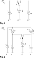
Ein Ausführungsbeispiel der Erfindung ist in
In
Diese Schaltung 100 weist neben dem lichtemittierenden Bauelement 20 zwei gegen ein Bezugspotential oder Referenzpotential W, insbesondere gegen Erdpotential oder Massepotential oder Nullpotential, betriebene Versorgungselemente in Form von Spannungsquellen 10 bzw. 10' (Akkumulatoreinheit) zur Versorgung der Schaltungsanordnung 100 mit erster Betriebsspannung U1 bzw. mit zweiter Betriebsspannung U2 auf.In addition to the light-emitting
Wie in
Dieses Schaltelement 30 ist zum Ansteuern des lichtemittierenden Bauelements 20 mittels Schaltens zumindest zwischen einer ersten Schaltposition und einer zweiten Schaltposition ausgebildet.This switching
Hierbei fällt in der ersten Schaltposition des Schaltelements 30 die gesamte oder nahezu die gesamte von der ersten Spannungsquelle 10 bereit gestellte Spannung U1 am lichtemittierenden Bauelement 20 ab; exemplarisch können in der ersten Schaltposition des Schaltelements 30 mindestens etwa neunzig Prozent, zum Beispiel etwa 99 Prozent, der von der ersten Spannungsquelle 10 bereit gestellten Spannung am lichtemittierenden Bauelement 20 abfallen.In this case, in the first switching position of the switching
Hingegen fällt in der zweiten Schaltposition des Schaltelements 30 die gesamte oder nahezu die gesamte von der zweiten Spannungsquelle 10' bereit gestellte Spannung U2 am lichtemittierenden Bauelement 20 ab; exemplarisch können in der zweiten Schaltposition des Schaltelements 30 mindestens etwa neunzig Prozent, zum Beispiel etwa 99 Prozent, der von der zweiten Spannungsquelle 10' bereit gestellten Spannung am lichtemittierenden Bauelement 20 abfallen.In contrast, in the second switching position of the switching
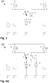
Die Schaltungsanordnung 100' gemäß dem anhand
Zur Versorgung mit Versorgungsspannung 14 (sogenannte Urspannung), zum Beispiel in der Größenordnung von etwa drei Volt, weist die Schaltungsanordnung 100' ein Versorgungselement in Form einer Batterie auf.For the supply with supply voltage 14 (so-called original voltage), for example in the order of magnitude of approximately three volts, the
Wie also in
Die Stromquelle 10 bzw. 10' dient hierbei zur bedarfsgemäßen Stromnachführung. Der Stützkondensator 12 bzw. 12' dient dazu, die Impedanz des Knotens N bzw. N' für den Bereich der Schalt- und Betriebsfrequenzen der Treiberschaltung 100' zu verringern.The
Da sich eine Erhöhung der Kapazität am Knotenpunkt N bzw. N' vorteilhaft auf die Stützwirkung an diesem Knotenpunkt N bzw. N' auswirkt, ist bei der Dimensionierung der Stromquelle 10 bzw. 10' keine Obergrenze für deren parasitäre Ausgangskapazität zu beachten, denn die Ausgestaltung gemäß
Hierdurch kann die Stromquelle 10 bzw. 10' so dimensioniert werden, dass sie auch bei sehr geringer Spannungsdifferenz zwischen der Versorgungsspannung 14 und der Spannung am Knotenpunkt N bzw. N' bestimmungsgemäß arbeitet.In this way, the
In der ersten Schaltposition des Schaltelements 30 wird das lichtemittierende Bauelement 20 mit dem Knotenpunkt N verbunden, an dem eine exemplarische Spannung von etwa 2,8 Volt anliegt. In der zweiten Schaltposition des Schaltelements 30 wird das lichtemittierende Bauelement 20 mit dem Knotenpunkt N' verbunden, an dem eine exemplarische Spannung von etwa 2,3 Volt anliegt.In the first switching position of the switching
Hierbei ist der den Ausgang der Stromquelle 10 bzw. 10' und die erste bzw. zweite Schaltposition des Schaltelements 30 verknüpfende Knotenpunkt N bzw. N' durch den Stützkondensator 12 bzw. 12' hochkapazitiv gestützt sowie mit dem zu übertragenden Signal im Wesentlichen "nicht bewegt", das heißt konstant.Here, the node N or N 'linking the output of the
Unter Berücksichtigung eines exemplarischen Spannungsverlustes am Schaltelement 30 in Höhe von beispielsweise etwa 0,1 Volt werden auf diese Weise beim lichtemittierenden Bauelement 20 hochfrequent zwischen etwa 2,7 Volt und etwa 2,2 Volt wechselnde Signale ermöglicht, denn durch die kapazitive Stützung der Knoten N bzw. N' wird "beidseitig" eine Abgrenzung oder Trennung zwischen dem niederfrequenten Zweig der Stromquelle 10, 10' und dem hochfrequenten Zweig des lichtemittierenden Bauelements 20 herbei geführt.Taking into account an exemplary voltage loss at the switching
Hierbei wirkt sich in vorteilhafter Weise aus, dass der niederkapazitive und kleinflächige Umschalter 30 so gut wie keinen kapazitiven Beitrag leistet und ein hochfrequentes, das heißt sehr schnelles Schalten zwischen den beiden im Wesentlichen statischen Zuständen ermöglicht.This has an advantageous effect that the low-capacitive and small-
Im Ergebnis ermöglicht die Schaltungsanordnung 100' gemäß dem anhand
Auch kann bei der Treiberschaltung 100' die Ausgangsimpedanz bei hohen Frequenzen sehr niedrig gehalten werden, denn diese Ausgangsimpedanz ist lediglich durch den parasitären Widerstand des Schaltelements 30 limitiert, so dass eine sehr hohe Betriebsfrequenz oder Schaltgeschwindigkeit erzielt werden kann.The output impedance of the
Im besonderen Fall der vorliegenden Erfindung kann eine sehr hohe Ausgangsspannung für das lichtemittierende Bauelement 20 erzielt werden, denn über den Schalter 30 erfolgt nur ein sehr geringer Spannungsabfall; zudem ist die Stromquelle 10, 10' vorteilhafterweise im Versorgungspfad und nicht im hochfrequenten Signalpfad angeordnet.In the particular case of the present invention, a very high output voltage can be achieved for the light-emitting
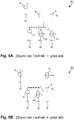
Bei der Schaltungsanordnung 100" gemäß dem anhand
Die Diode 30' übernimmt hierbei die Funktion der zweiten (, in
Eine eventuell nicht vernachlässigbare Durchlassspannung der in Vorwärtsrichtung gepolten Diode 30', zum Beispiel in der Größenordnung von etwa 0,2 Volt im Falle einer Schottky-Diode, führt zu einem entsprechend großen Spannungsverlust zwischen der Spannung am Knotenpunkt N' und der dem lichtemittierenden Bauelement 20 zur Verfügung stehenden Betriebsspannung.A possibly non-negligible forward voltage of the forward-polarized diode 30 ', for example in the order of about 0.2 volts in the case of a Schottky diode, leads to a correspondingly large voltage loss between the voltage at the node N' and that of the light-emitting
Da dieser Spannungsverlust aber nur bei derjenigen Schaltposition auftritt, der beabsichtigterweise eine verringerte Betriebsspannung am lichtemittierenden Bauelement 20 zugeordnet ist, kann eine Kompensation des Spannungsverlusts durch Anheben der Spannung am Knotenpunkt N' erfolgen.Since this voltage loss only occurs in the switching position that is intentionally assigned a reduced operating voltage at the light-emitting
Bei der Schaltungsanordnung 100'" gemäß dem anhand
- dessen Drainanschluss D' mit dem zweiten Knotenpunkt N',
- dessen Gateanschluss G'
mit einem Stützversorgungselement 34, insbesondere mit einer Stützspannungsquelle (zum Beispiel etwa 2,8 Volt), und - dessen Sourceanschluss S' mit dem Eingangsanschluss des lichtemittierenden Bauelements 20 verbunden ist.
- its drain connection D 'with the second node N',
- its gate connection G 'with a
backup supply element 34, in particular with a backup voltage source (for example about 2.8 volts), and - whose source connection S ′ is connected to the input connection of the light-emitting
component 20.
Die Kennlinie für den Drainstrom ID' dieses n-Kanal-MOSFET 30' ist in
In einer zu
- deren jeweilige Drainanschlüsse D bzw. D' über den Knoten N bzw. N' mit der ersten Stromquelle 10 bzw. mit der zweiten Stromquelle 10' verbunden sind,
- deren Gateanschluss G mit einer
Steuerungseinrichtung 40, zum Beispiel in Form einer Signalquelle, bzw. deren Gateanschluss G' überein optionales Widerstandselement 50 mit einer Stützspannungsquelle odermit einem Stützversorgungselement 34 verbunden ist und - deren jeweilige Sourceanschlüsse S bzw. S' miteinander sowie mit dem Eingangsanschluss des lichtemittierenden Bauelements 20 verbunden sind.
- whose respective drain connections D and D 'are connected via the node N or N' to the first
current source 10 and to the second current source 10 ', respectively, - whose gate connection G is connected to a
control device 40, for example in the form of a signal source, or whose gate connection G 'is connected via anoptional resistance element 50 to a backup voltage source or to abackup supply element 34, and - whose respective source connections S and S ′ are connected to one another and to the input connection of the light-emitting
component 20.
Hierbei ist bei der anhand
- dessen erster Eingangsanschluss mit der zweiten kapazitiv gestützten Stromquelle 10' verbunden ist,
- dessen optionaler zweiter Eingangsanschluss mit einer optionalen Referenzspannungsquelle 26 verbunden ist und
- dessen Ausgangsanschluss
mit dem Stützversorgungselement 34 verbunden ist.
- whose first input connection is connected to the second capacitively supported current source 10 ',
- the optional second input terminal of which is connected to an optional
reference voltage source 26 and - the output connection of which is connected to the
support supply element 34.
Ein derartiges Regelungs-/Verarbeitungselement 22 kann - obwohl in
Der Komparator oder Verstärker 22 ist dazu ausgebildet,
- die am Knotenpunkt N' anliegende Spannung zu ermitteln,
- die ermittelte Spannung mit der durch die
Referenzspannungsquelle 26 bereit gestellten Referenzspannung Vref zu vergleichen und - im Bedarfsfalle die Spannung des Stützversorgungselements 34 dergestalt nachzuregeln oder zu steuern, insbesondere dergestalt anzuheben oder abzusenken, dass sich die Spannung am Knotenpunkt N' dem Wert der Referenzspannung Vref annähert.
- determine the voltage present at the node N ',
- to compare the determined voltage with the reference voltage Vref provided by the
reference voltage source 26 and - If necessary, readjust or control the voltage of the
backup supply element 34 in such a way, in particular raise or lower it in such a way that the voltage at the node N 'approaches the value of the reference voltage Vref.
Grundsätzlich kann die vorliegende Erfindung in vielfältiger Weise ausgestaltet werden; insbesondere durch Hinzufügen zusätzlicher Bauelemente oder zusätzlicher Bauteile in die Signal- und Regelpfade lässt sich die vorliegende Erfindung an bestimmte Erfordernisse anpassen.In principle, the present invention can be designed in a variety of ways; In particular, by adding additional components or additional components to the signal and control paths, the present invention can be adapted to specific requirements.
Exemplarisch sei auf das optionale Widerstandselement 50 in
In diesem Zusammenhang sei darauf aufmerksam gemacht, dass der Begriff "Verbindung" im Rahmen der vorliegenden Erfindung auch Verbindungen oder Verbindungsarten umfasst, die durch zusätzlich eingebrachte Bauelemente oder Bauteile erfolgen.In this context, attention should be drawn to the fact that the term “connection” in the context of the present invention also includes connections or types of connection which are made by additionally introduced components or components.
- 100100
-
Schaltungsanordnung, insbesondere Ansteuerschaltung oder Treiberschaltung (= vgl.
Fig. 1 )Circuit arrangement, in particular control circuit or driver circuit (= cf.Fig. 1 ) - 100'100 '
-
Schaltungsanordnung, insbesondere Ansteuerschaltung oder Treiberschaltung (= vgl.
Fig. 2 )Circuit arrangement, in particular control circuit or driver circuit (= cf.Fig. 2 ) - 100"100 "
-
Schaltungsanordnung, insbesondere Ansteuerschaltung oder Treiberschaltung (= vgl.
Fig. 3 )Circuit arrangement, in particular control circuit or driver circuit (= cf.Fig. 3 ) - 100'"100 '"
-
Schaltungsanordnung, insbesondere Ansteuerschaltung oder Treiberschaltung (=Ausführungsbeispiel der vorliegenden Erfindung; vgl.
Fig. 4C und auchFigur 4A ).Circuit arrangement, in particular control circuit or driver circuit (= exemplary embodiment of the present invention; cf.Figure 4C and alsoFigure 4A ).
- 1010
-
erstes Versorgungselement, insbesondere erste Spannungsquelle, beispielsweise erste Akkumulatoreinheit, zum Versorgen der Schaltungsanordnung 100, 100', 100", 100'" mit Spannung, insbesondere mit Gleichspannungfirst supply element, in particular first voltage source, for example first accumulator unit, for supplying
circuit arrangement - 10'10 '
-
zweites Versorgungselement, insbesondere zweite Spannungsquelle, beispielsweise zweite Akkumulatoreinheit, zum Versorgen der Schaltungsanordnung 100, 100', 100", 100'" mit Spannung, insbesondere mit Gleichspannungsecond supply element, in particular a second voltage source, for example a second accumulator unit, for supplying the
circuit arrangement - 1212th
-
Stützkondensator, insbesondere kapazitive Stützung, des ersten Versorgungselements 10Support capacitor, in particular capacitive support, of the
first supply element 10 - 12'12 '
- Stützkondensator, insbesondere kapazitive Stützung, des zweiten Versorgungselements 10'Support capacitor, in particular capacitive support, of the second supply element 10 '
- 1414th
-
Versorgungsspannung, insbesondere Urspannung, des Versorgungselements 10, 10'Supply voltage, in particular original voltage, of the
supply element 10, 10 ' - 2020th
- lichtemittierendes Bauelement, insbesondere elektrooptischer Wandler, beispielsweise lichtemittierende Diode (= L[ight]E[mitting]D[iode]) bzw. Leuchtdiode oder Laser, wie etwa Halbleiterlaserlight-emitting component, in particular electro-optical converter, for example light-emitting diode (= L [ight] E [mitting] D [iode]) or light-emitting diode or laser, such as semiconductor laser
- 2222nd
- Regelungs- und/oder Verarbeitungselement, insbesondere Komparator und/oder Verstärker, zum Beispiel OperationsverstärkerControl and / or processing element, in particular a comparator and / or amplifier, for example an operational amplifier
- 2626th
- Bezugsspannungsquelle oder ReferenzspannungsquelleReference voltage source or reference voltage source
- 3030th
- Schaltelement, insbesondere Einschalter oder Umschalter oder Wechselschalter, beispielsweise Schalttransistor, wie etwa M[etal]O[xide]S[emiconductor]F[ield]E[ffect]T[ransistor oder MOSTransistor, zum Beispiel n-Kanal-F[eld]E[ffekt]T[ransistor]Switching element, in particular on switch or changeover switch or changeover switch, for example switching transistor, such as M [etal] O [xide] S [emiconductor] F [ield] E [ffect] transistor or MOS transistor, for example n-channel F [eld] E [ffect] T [ransistor]
- 30'30 '
-
zweite Komponente des Schaltelements 30, insbesondere in Vorwärtsrichtung, insbesondere zum Schaltelement 30 hin, gepolte Diode, zum Beispiel pn-Diode oder Schottky-Diode und/oder Schalttransistor, beispielsweise M[etal]O[xide]S[emiconductor]F[ield]E[ffect]T[ransistor oder MOSTransistor, zum Beispiel n-Kanal-F[eld]E[ffekt]T[ransistor]second component of the switching
element 30, in particular in the forward direction, in particular towards the switchingelement 30, polarized diode, for example pn diode or Schottky diode and / or switching transistor, for example M [etal] O [xide] S [emiconductor] F [ield] E [ffect] T [ransistor or MOSTransistor, for example n-channel F [eld] E [ffect] T [ransistor] - 3434
- Stützversorgungselement, insbesondere Stützspannungsquelle, des Transistors 30'Support supply element, in particular support voltage source, of transistor 30 '
- 4040
-
Steuerungseinrichtung, insbesondere Signalquelle, des Transistors 30Control device, in particular signal source, of
transistor 30 - 5050
- Widerstand, insbesondere Ohmsches WiderstandselementResistance, especially ohmic resistance element
- CC.
-
Kondensator (= drittes Beispiel aus dem Stand der Technik; vgl.
Fig. 5C )Capacitor (= third example from the prior art; cf.Figure 5C ) - DD.
-
Drainanschluss des Transistors 30Drain connection of
transistor 30 - D'D '
- Drainanschluss des Transistors 30'Drain connection of transistor 30 '
- EE.
-
lichtemittierendes Bauelement, insbesondere elektrooptischer Wandler, beispielsweise lichtemittierende Diode (= L[ight]E[mitting]D[iode]) bzw. Leuchtdiode oder Laser, wie etwa Halbleiterlaser (= Beispiele aus dem Stand der Technik; vgl.
Fig. 5A, Fig. 5B ,Fig. 5C )light-emitting component, in particular electro-optical converter, for example light-emitting diode (= L [ight] E [mitting] D [iode]) or light-emitting diode or laser, such as semiconductor laser (= examples from the prior art; cf.Figures 5A, 5B ,Figure 5C ) - GG
-
Gateanschluss des Transistors 30Gate connection of
transistor 30 - G'G'
- Gateanschluss des Transistors 30'Gate connection of transistor 30 '
- K1K1
-
weitere Schaltungskomponente, nämlich Konstantstromquelle für I1 (= Beispiele aus dem Stand der Technik; vgl.
Fig. 5A, Fig. 5B ,Fig. 5C )further circuit components, namely constant current source for I 1 (= examples from the prior art; cf.Figures 5A, 5B ,Figure 5C ) - K2K2
-
zweite weitere Schaltungskomponente, nämlich Konstantstromquelle für I2 (= Beispiele aus dem Stand der Technik; vgl.
Fig. 5A, Fig. 5B ,Fig. 5C )second further circuit component, namely constant current source for I 2 (= Examples from the state of the art; cf.Figures 5A, 5B ,Figure 5C ) - K2'K2 '
-
dritte weitere Schaltungskomponente, nämlich Konstantstromquelle für I2/2 (= drittes Beispiel aus dem Stand der Technik; vgl.
Fig. 5C )third further circuit component, namely constant current source for I 2/2 (= third example from the prior art; cf.Figure 5C ) - LL.
-
Spule (= drittes Beispiel aus dem Stand der Technik; vgl.
Fig. 5C )Coil (= third example from the prior art; cf.Figure 5C ) - NN
-
erster, insbesondere niederohmscher, Knoten oder Knotenpunkt zwischen erstem Versorgungselement 10, erstem Stützkondensator 12 und erster Schaltposition des Schaltelements 30first, in particular low-resistance, node or node between the
first supply element 10, thefirst backup capacitor 12 and the first switching position of the switchingelement 30 - N'N '
-
zweiter, insbesondere niederohmscher, Knoten oder Knotenpunkt zwischen zweitem Versorgungselement 10, zweitem Stützkondensator 12 und zweiter Schaltposition des Schaltelements 30Second, in particular low-resistance, node or node between the
second supply element 10, thesecond backup capacitor 12 and the second switching position of the switchingelement 30 -
Spannungsquelle, insbesondere Akkumulatoreinheit oder Akku (= Beispiele aus dem Stand der Technik; vgl.
Fig. 5A, Fig. 5B ,Fig. 5C )Voltage source, in particular accumulator unit or battery (= examples from the prior art; cf.Figures 5A, 5B ,Figure 5C ) - RR.
-
Blindlast (= erstes Beispiel aus dem Stand der Technik; vgl.
Fig. 5A )Reactive load (= first example from the state of the art; cf.Figure 5A ) - SS.
-
Sourceanschluss des Transistors 30Source terminal of
transistor 30 - S'S '
- Sourceanschluss des Transistors 30'Source connection of transistor 30 '
- S1S1
-
Schaltungsanordnung (= erstes Beispiel aus dem Stand der Technik; vgl.
Fig. 5A )Circuit arrangement (= first example from the prior art; cf.Figure 5A ) - S2S2
-
Schaltungsanordnung (= zweites Beispiel aus dem Stand der Technik; vgl.
Fig. 5B )Circuit arrangement (= second example from the prior art; cf.Figure 5B ) - S3S3
-
Schaltungsanordnung (= drittes Beispiel aus dem Stand der Technik; vgl.
Fig. 5C )Circuit arrangement (= third example from the prior art; cf.Figure 5C ) - TT
-
Steuerungseinrichtung, insbesondere Signalquelle, zum Steuern (des Schaltens) des Schaltelements U, insbesondere Einschaltersteuerung oder Umschaltersteuerung oder Wechselschaltersteuerung (= Beispiele aus dem Stand der Technik; vgl.
Fig. 5A, Fig. 5B ,Fig. 5C )Control device, in particular signal source, for controlling (switching) the switching element U, in particular on-switch control or changeover switch control or changeover switch control (= examples from the prior art; cf.Figures 5A, 5B ,Figure 5C ) - UU
-
Schaltelement, insbesondere Einschalter oder Umschalter oder Wechselschalter (= Beispiele aus dem Stand der Technik; vgl.
Fig. 5A, Fig. 5B ,Fig. 5C )Switching element, in particular on switch or changeover switch or changeover switch (= examples from the prior art; cf.Figures 5A, 5B ,Figure 5C ) - VrefVref
-
durch Bezugsspannungsquelle 26 bereit gestellte Bezugsspannung oder durch Referenzspannungsquelle 26 bereit gestellte Referenzspannungreference voltage provided by
reference voltage source 26 or reference voltage provided byreference voltage source 26 - WW.
- Bezugspotential oder Referenzpotential, insbesondere Erdpotential oder Massepotential oder NullpotentialReference potential or reference potential, in particular earth potential or ground potential or zero potential
Claims (7)
- A circuit arrangement (100"; 100"'), in particular a driver circuit, for controlling at least one light-emitting component (20), embodied as at least one light-emitting diode or electroluminescent diode or as at least one semiconductor laser, wherein the circuit arrangement (100"; 100"') comprises:- at least two supply elements (10; 10') connected to one another in parallel, each embodied as a current source capacitively, in particular by means of at least one decoupling capacitor (12; 12'), supported on the output side, said supply elements (10; 10') provided for supplying the circuit arrangement (100"; 100"') with voltage, said supply elements (10; 10') connected to at least one supply voltage, in particular to at least one Thevenin voltage or to at least one voltage source (14), for example to at least one battery, and fed by the supply voltage,- at least one switching element (30) connecting the output terminal of the first supply element (10) to the input terminal of the light-emitting component (20) and switchable at least between a first switching position and a second switching position, and- at least one transistor (30') connected between at least one of the supply elements (10; 10') and the switching element (30), namely connecting the output terminal of the second supply element (10') to the input terminal of the light-emitting component (20),- the drain terminal (D') of said transistor (30') connected to the first supply element (10) or to the second supply element (10'),- the gate terminal (G') of said transistor (30') connected to at least one supporting supply element (34), in particular to at least one supporting voltage source, and- the source terminal (S') of said transistor (30') connected to the input terminal of the light-emitting component (20),so that the light-emitting component (20)-- is supplyable with a first operating voltage in the first switching position of the switching element (30), said first operating voltage provided by the first supply element (10),-- is supplyable with a second operating voltage in the second switching position of the switching element (30), said second operating voltage provided by the second supply element (10'), and-- is controllable by switching between the first operating voltage and the second operating voltage,characterized by at least one regulating and/or processing element (22), in particular by at least one comparator and/or by at least one amplifier,- the first input terminal of which is connected to the second supply element (10'), in particular to the second current source capacitively supported on the output side,- the second input terminal of which is connected to at least one reference voltage source (26), and- the output terminal of which is connected to the supporting supply element (34).
- The circuit arrangement according to claim 1, characterized in that at least one diode (30') polarized in the forward direction, in particular towards the switching element (30), for example at least one pn diode or at least one Schottky diode, is connected between at least one of the supply elements (10; 10') and the switching element (30).
- The circuit arrangement according to claim 1 or 2, characterized in that the switching element is embodied as at least two transistors (30 or 30'),- the respective drain terminal (D or D') of which is connected to the first supply element (10) or to the second supply element (10'),- the gate terminal (G) of which is connected to at least one control device (40), in particular to at least one signal source, or the gate terminal (G') of which connected, in particular via at least one resistance element (50), to at least one supporting supply element (34), in particular to at least one supporting voltage source, and- the respective source terminals (S or S') of which are connected to one another as well as to the input terminal of the light-emitting component (20).
- The circuit arrangement according to at least one of claims 1 to 3, characterized in that the transistor (30') is or the transistors (30; 30') are embodied as at least one or two M[etal]O[xide]S[emiconductor]F[ield]E[ffect]T[ransistor](s) or as at least one or two MOS transistor(s), in particular as at least one or two n-channel F[ield]E[ffect]T[ransistor](s).
- A method for controlling at least one light-emitting component (20), embodied as at least one light-emitting diode or electroluminescent diode or as at least one semiconductor laser, by varying its operating voltage by means of at least one circuit arrangement (100"; 100'"), in particular by means of at least one driver circuit, according to at least one of claims 1 to 4,
wherein the light-emitting component (20)-- is supplied with a first operating voltage in the first switching position of the switching element (30),-- is supplied with a second operating voltage in the second switching position of the switching element (30), and-- is controlled by switching between the first operating voltage and the second operating voltage, - The method according to claim 5, characterized in that the operating voltage of the light-emitting component (20) is varied by means of switching between the switching positions, of which at least the first switching position and the second switching position are of low impedance for the operating frequency.
- Use of at least one circuit arrangement (100"; 100'"), in particular of at least one driver circuit, according to at least one of claims 1 to 4 and/or of a method according to claim 5 or 6- in at least one, in particular mobile, telecommunication system, for example in at least one communication device, such as in at least one mobile telephone,- in at least one, in particular mobile, data communication system or in at least one, in particular mobile, data processing device, for example in at least one handheld, in at least one notebook or in at least one P[ersonal]D[igital]A[ssistant],- in at least one, in particular mobile, data recording and/or reproducing device, for example in at least one camcorder, in at least one digital camera or in at least one H[igh]D[efinition]T[ele]V[ision], or- in at least one transportation means, for example in at least one driver assistance system or in at least one navigation system of an automobile.
Applications Claiming Priority (4)
| Application Number | Priority Date | Filing Date | Title |
|---|---|---|---|
| DE102007028576 | 2007-06-19 | ||
| DE102007040151 | 2007-08-24 | ||
| DE102008001453 | 2008-04-29 | ||
| PCT/EP2008/057785 WO2008155385A1 (en) | 2007-06-19 | 2008-06-19 | Circuit arrangement and method for controlling light-emitting components |
Publications (2)
| Publication Number | Publication Date |
|---|---|
| EP2160927A1 EP2160927A1 (en) | 2010-03-10 |
| EP2160927B1 true EP2160927B1 (en) | 2021-04-14 |
Family
ID=39739846
Family Applications (1)
| Application Number | Title | Priority Date | Filing Date |
|---|---|---|---|
| EP08761220.6A Active EP2160927B1 (en) | 2007-06-19 | 2008-06-19 | Circuit arrangement and method for controlling light-emitting components |
Country Status (4)
| Country | Link |
|---|---|
| US (2) | US8855154B2 (en) |
| EP (1) | EP2160927B1 (en) |
| JP (2) | JP6076580B2 (en) |
| WO (1) | WO2008155385A1 (en) |
Families Citing this family (12)
| Publication number | Priority date | Publication date | Assignee | Title |
|---|---|---|---|---|
| JP6076580B2 (en) * | 2007-06-19 | 2017-02-08 | シリコン・ライン・ゲー・エム・ベー・ハー | Circuit device for controlling light emitting components |
| EP2359502B1 (en) | 2008-10-09 | 2017-04-05 | Silicon Line GmbH | Circuit arrangement and method for transmitting tmds encoded signals |
| US8399819B2 (en) * | 2009-03-31 | 2013-03-19 | Osram Sylvania Inc. | Current source to drive a light source in an optical sensor system |
| DE102010018865B4 (en) * | 2010-04-30 | 2015-11-26 | Austriamicrosystems Ag | Driver circuit for light-emitting diodes and methods |
| FR2971105A1 (en) * | 2011-01-31 | 2012-08-03 | Aeg Power Solutions Bv | Output stage for converter for public lighting, has switch alternatively switching current through inductor between direct current input voltage and non-zero direct current input voltage not corresponding to zero voltage to shut off LEDs |
| US10097908B2 (en) * | 2014-12-31 | 2018-10-09 | Macom Technology Solutions Holdings, Inc. | DC-coupled laser driver with AC-coupled termination element |
| US9753060B2 (en) | 2015-08-28 | 2017-09-05 | Stmicroelectronics (Research & Development) Limited | Apparatus with device with fault detection protection |
| US10033155B2 (en) * | 2016-11-23 | 2018-07-24 | Stmicroelectronics (Research & Development) Limited | Circuit and method of operating a laser diode |
| US10808860B2 (en) | 2017-10-24 | 2020-10-20 | Mac Valves, Inc. | Latching pneumatic control valve |
| JP7083674B2 (en) * | 2018-03-22 | 2022-06-13 | 株式会社マキタ | Portable blower |
| DE102018106959A1 (en) | 2018-03-23 | 2019-09-26 | Osram Opto Semiconductors Gmbh | OPTOELECTRONIC COMPONENT AND METHOD FOR PRODUCING AN OPTOELECTRONIC COMPONENT |
| US11510297B2 (en) * | 2018-12-24 | 2022-11-22 | Beijing Voyager Technology Co., Ltd. | Adaptive power control for pulsed laser diodes |
Citations (1)
| Publication number | Priority date | Publication date | Assignee | Title |
|---|---|---|---|---|
| US20060133435A1 (en) * | 2001-03-05 | 2006-06-22 | Fuji Xerox Co., Ltd. | Apparatus for driving light emitting element and system for driving light emitting element |
Family Cites Families (50)
| Publication number | Priority date | Publication date | Assignee | Title |
|---|---|---|---|---|
| FR2654876B1 (en) * | 1989-11-23 | 1993-11-12 | Commissariat A Energie Atomique | DEVICE FOR CHARGING MEANS OF ACCUMULATING ELECTRICAL ENERGY, PROVIDED WITH MEANS FOR CONTROLLING THIS LOAD. |
| US5012384A (en) * | 1990-02-20 | 1991-04-30 | Advanced Micro Device, Inc. | Load circuit for a differential driver |
| US5019769A (en) * | 1990-09-14 | 1991-05-28 | Finisar Corporation | Semiconductor laser diode controller and laser diode biasing control method |
| JP2891832B2 (en) * | 1992-11-10 | 1999-05-17 | 日本電気アイシーマイコンシステム株式会社 | LCD driver circuit |
| JPH08288816A (en) * | 1995-04-18 | 1996-11-01 | Rohm Co Ltd | Switching circuit |
| US5672994A (en) * | 1995-12-21 | 1997-09-30 | International Business Machines Corporation | Antifuse circuit using standard MOSFET devices |
| JP3725235B2 (en) * | 1996-03-29 | 2005-12-07 | 富士通株式会社 | Light emitting element driving circuit and light emitting device having the same |
| US5834813A (en) * | 1996-05-23 | 1998-11-10 | Micron Technology, Inc. | Field-effect transistor for one-time programmable nonvolatile memory element |
| US5949253A (en) * | 1997-04-18 | 1999-09-07 | Adaptec, Inc. | Low voltage differential driver with multiple drive strengths |
| JP2001326569A (en) * | 2000-05-16 | 2001-11-22 | Toshiba Corp | Led driving circuit and optical transmission module |
| GB2365788A (en) * | 2000-08-10 | 2002-02-27 | Mark Technology Corp Q | A signal transmitting/flashing adapter for a hand-held electronic game |
| EP1233453A3 (en) * | 2001-02-19 | 2005-03-23 | Kawasaki Microelectronics, Inc. | Semiconductor integrated circuit having anti-fuse, method of fabricating, and method of writing data in the same |
| US6667661B1 (en) * | 2001-05-04 | 2003-12-23 | Euvis, Inc. | Laser diode driver with high power efficiency |
| EP1427076B1 (en) * | 2001-08-23 | 2007-01-17 | Sony Corporation | Semiconductor laser optical output control circuit and optical device |
| US6545928B1 (en) * | 2001-09-25 | 2003-04-08 | Micron Technology, Inc. | Antifuse programming current limiter |
| US6686772B2 (en) * | 2001-11-19 | 2004-02-03 | Broadcom Corporation | Voltage mode differential driver and method |
| JP4177022B2 (en) * | 2002-05-07 | 2008-11-05 | ローム株式会社 | LIGHT EMITTING ELEMENT DRIVE DEVICE AND ELECTRONIC DEVICE HAVING LIGHT EMITTING ELEMENT |
| JP2003332623A (en) * | 2002-05-07 | 2003-11-21 | Rohm Co Ltd | Light emitting element drive device and electronic apparatus having light emitting element |
| US6650143B1 (en) * | 2002-07-08 | 2003-11-18 | Kilopass Technologies, Inc. | Field programmable gate array based upon transistor gate oxide breakdown |
| US6812733B1 (en) * | 2002-08-02 | 2004-11-02 | Pmc-Sierra, Inc. | High-efficiency mixed voltage/current mode output driver |
| US7339963B2 (en) * | 2002-11-27 | 2008-03-04 | International Business Machines Corporation | High speed data channel including a CMOS VCSEL driver and a high performance photodetector and CMOS photoreceiver |
| US6975135B1 (en) * | 2002-12-10 | 2005-12-13 | Altera Corporation | Universally programmable output buffer |
| US7545839B2 (en) * | 2003-01-02 | 2009-06-09 | Optiswitch Technology Corporation | Apparatus and method for driving a pulsed laser diode |
| US6897543B1 (en) * | 2003-08-22 | 2005-05-24 | Altera Corporation | Electrically-programmable integrated circuit antifuses |
| US7262584B2 (en) * | 2004-02-19 | 2007-08-28 | Analog Modules, Inc | Efficient fast pulsed laser or light-emitting diode driver |
| US7133429B2 (en) * | 2004-03-05 | 2006-11-07 | Finisar Corporation | Laser driver circuit with signal transition enhancement |
| JP4552583B2 (en) * | 2004-03-26 | 2010-09-29 | セイコーエプソン株式会社 | Noise detection apparatus, noise detection method, and noise detection program |
| JP4241487B2 (en) * | 2004-04-20 | 2009-03-18 | ソニー株式会社 | LED driving device, backlight light source device, and color liquid crystal display device |
| KR101066414B1 (en) * | 2004-05-19 | 2011-09-21 | 재단법인서울대학교산학협력재단 | Driving element and driving method of organic light emitting device, and display panel and display device having the same |
| DE102004032456B3 (en) | 2004-06-30 | 2006-04-06 | Siemens Ag | Circuit arrangement for operating illuminated sign e.g. for railway safety installations, and motor vehicles, has constant current sources which are fed from common voltage source |
| US7154923B2 (en) * | 2004-08-24 | 2006-12-26 | International Business Machines Corporation | Method and apparatus for providing a modulation current |
| US6965722B1 (en) * | 2004-10-29 | 2005-11-15 | Finisar Corporation | High efficiency active matching electro-optic transducer driver circuit operable with low supply voltages |
| KR100652391B1 (en) * | 2004-12-17 | 2006-12-01 | 삼성전자주식회사 | Low voltage differential signaling driver |
| JP2006186277A (en) * | 2004-12-28 | 2006-07-13 | Sanyo Electric Co Ltd | Light-emitting element driving device |
| JP5025913B2 (en) * | 2005-05-13 | 2012-09-12 | シャープ株式会社 | LED drive circuit, LED illumination device, and backlight |
| FR2889643A1 (en) | 2005-08-08 | 2007-02-09 | Valeo Systemes Thermiques | Control board`s light intensity adjusting device for motor vehicle, has light sources supplied with supply currents from control interfaces, and control correctors modulating current in light sources according to required luminance |
| US7280425B2 (en) * | 2005-09-30 | 2007-10-09 | Intel Corporation | Dual gate oxide one time programmable (OTP) antifuse cell |
| US7173851B1 (en) | 2005-10-18 | 2007-02-06 | Kilopass Technology, Inc. | 3.5 transistor non-volatile memory cell using gate breakdown phenomena |
| US7400310B2 (en) * | 2005-11-28 | 2008-07-15 | Draeger Medical Systems, Inc. | Pulse signal drive circuit |
| WO2007069104A1 (en) | 2005-12-12 | 2007-06-21 | Koninklijke Philips Electronics N.V. | System and method for opening web links in a browser application |
| DE102005062486B4 (en) * | 2005-12-27 | 2007-10-31 | Insta Elektro Gmbh | Electrical / electronic installation device |
| TWI325130B (en) * | 2006-01-12 | 2010-05-21 | Himax Display Inc | Led current driving system for lcos display |
| US7978741B2 (en) * | 2006-06-14 | 2011-07-12 | Sumitomo Electric Industries, Ltd. | Optical transmitter with a shunt driving configuration and a load transistor operated in common gate mode |
| US8188682B2 (en) * | 2006-07-07 | 2012-05-29 | Maxim Integrated Products, Inc. | High current fast rise and fall time LED driver |
| US7312513B1 (en) * | 2006-07-10 | 2007-12-25 | Wilcox William J | Antifuse circuit with well bias transistor |
| US8324816B2 (en) | 2006-10-18 | 2012-12-04 | Koa Corporation | LED driving circuit |
| US20080304527A1 (en) * | 2007-06-07 | 2008-12-11 | Miaobin Gao | Controlling a bias current for an optical source |
| JP6076580B2 (en) * | 2007-06-19 | 2017-02-08 | シリコン・ライン・ゲー・エム・ベー・ハー | Circuit device for controlling light emitting components |
| WO2009007464A1 (en) * | 2007-07-12 | 2009-01-15 | Silicon Line Gmbh | Circuit arrangement and method for driving at least one differential line |
| WO2009127670A1 (en) * | 2008-04-16 | 2009-10-22 | Silicon Line Gmbh | Programmable antifuse transistor and method for programming thereof |
-
2008
- 2008-06-19 JP JP2010512688A patent/JP6076580B2/en active Active
- 2008-06-19 WO PCT/EP2008/057785 patent/WO2008155385A1/en active Application Filing
- 2008-06-19 EP EP08761220.6A patent/EP2160927B1/en active Active
-
2009
- 2009-12-22 US US12/654,515 patent/US8855154B2/en active Active
-
2014
- 2014-10-06 US US14/507,604 patent/US20150023378A1/en not_active Abandoned
-
2016
- 2016-05-06 JP JP2016093461A patent/JP6240707B2/en not_active Expired - Fee Related
Patent Citations (1)
| Publication number | Priority date | Publication date | Assignee | Title |
|---|---|---|---|---|
| US20060133435A1 (en) * | 2001-03-05 | 2006-06-22 | Fuji Xerox Co., Ltd. | Apparatus for driving light emitting element and system for driving light emitting element |
Also Published As
| Publication number | Publication date |
|---|---|
| JP6240707B2 (en) | 2017-11-29 |
| US8855154B2 (en) | 2014-10-07 |
| JP2016167627A (en) | 2016-09-15 |
| US20150023378A1 (en) | 2015-01-22 |
| JP2010533363A (en) | 2010-10-21 |
| EP2160927A1 (en) | 2010-03-10 |
| WO2008155385A1 (en) | 2008-12-24 |
| JP6076580B2 (en) | 2017-02-08 |
| US20100172385A1 (en) | 2010-07-08 |
Similar Documents
| Publication | Publication Date | Title |
|---|---|---|
| EP2160927B1 (en) | Circuit arrangement and method for controlling light-emitting components | |
| EP2172082B1 (en) | Circuit arrangement and method for controlling light-emitting components | |
| DE102011010506B4 (en) | microphone array | |
| DE112010004476T5 (en) | Receiving circuit for visible light | |
| DE4302056A1 (en) | Resonant inverter | |
| EP0562359A1 (en) | Laserdiode control circuit | |
| DE112016006788B4 (en) | Integrated semiconductor circuit, sensor reading device and sensor reading process | |
| EP0570820B1 (en) | Switchable current source circuit and the use of such a circuit in a phase detector | |
| DE102017205651A1 (en) | DEVICE AND METHOD OF A SLOPING REGULATOR AND REGULATION OF THE INCREASE OF SWITCHING POWER FETS | |
| DE60310426T2 (en) | DRIVER FOR ANALOG LOADS | |
| DE10357785B3 (en) | Linear switched capacitor circuit device using integrated deep-sub-micron technology has thick oxide transistors used in switched capacitor circuit | |
| DE102014119195B4 (en) | Electro-optical modulator | |
| EP0277377A1 (en) | Current limiting circuit | |
| EP1388200B1 (en) | Circuit arrangement for voltage stabilisation | |
| EP2471202B1 (en) | Circuit assembly for setting the voltage potential at the rf output of a pin photoreceiver and photoreceiver assembly | |
| DE19835198A1 (en) | Process for generating an alternating voltage with a quartz-stabilized frequency and Pierce oscillator amplifier for carrying out the process | |
| DE102022201070A1 (en) | Electro-optical mixer | |
| EP2672311B1 (en) | Method for selecting optical pulses | |
| WO2009141449A2 (en) | Circuit arrangement and method for controlling light emitting components | |
| DE102005004391A1 (en) | filter circuit | |
| DE2655320C2 (en) | ||
| DE102008051633B4 (en) | Compensation for a capacitive load driving amplifier | |
| EP1497914B1 (en) | Sensor circuit | |
| EP1267487A1 (en) | High frequency amplifier | |
| EP0422273A1 (en) | Duty cycle regulator circuit arrangement |
Legal Events
| Date | Code | Title | Description |
|---|---|---|---|
| PUAI | Public reference made under article 153(3) epc to a published international application that has entered the european phase |
Free format text: ORIGINAL CODE: 0009012 |
|
| 17P | Request for examination filed |
Effective date: 20100114 |
|
| AK | Designated contracting states |
Kind code of ref document: A1 Designated state(s): AT BE BG CH CY CZ DE DK EE ES FI FR GB GR HR HU IE IS IT LI LT LU LV MC MT NL NO PL PT RO SE SI SK TR |
|
| AX | Request for extension of the european patent |
Extension state: AL BA MK RS |
|
| DAX | Request for extension of the european patent (deleted) | ||
| 17Q | First examination report despatched |
Effective date: 20120807 |
|
| STAA | Information on the status of an ep patent application or granted ep patent |
Free format text: STATUS: EXAMINATION IS IN PROGRESS |
|
| RAP1 | Party data changed (applicant data changed or rights of an application transferred) |
Owner name: SILICON LINE GMBH |
|
| REG | Reference to a national code |
Ref country code: DE Ref legal event code: R079 Ref document number: 502008017199 Country of ref document: DE Free format text: PREVIOUS MAIN CLASS: H05B0033080000 Ipc: H05B0045370000 |
|
| GRAP | Despatch of communication of intention to grant a patent |
Free format text: ORIGINAL CODE: EPIDOSNIGR1 |
|
| STAA | Information on the status of an ep patent application or granted ep patent |
Free format text: STATUS: GRANT OF PATENT IS INTENDED |
|
| RIC1 | Information provided on ipc code assigned before grant |
Ipc: H05B 45/37 20200101AFI20201005BHEP |
|
| INTG | Intention to grant announced |
Effective date: 20201029 |
|
| GRAS | Grant fee paid |
Free format text: ORIGINAL CODE: EPIDOSNIGR3 |
|
| GRAA | (expected) grant |
Free format text: ORIGINAL CODE: 0009210 |
|
| STAA | Information on the status of an ep patent application or granted ep patent |
Free format text: STATUS: THE PATENT HAS BEEN GRANTED |
|
| AK | Designated contracting states |
Kind code of ref document: B1 Designated state(s): AT BE BG CH CY CZ DE DK EE ES FI FR GB GR HR HU IE IS IT LI LT LU LV MC MT NL NO PL PT RO SE SI SK TR |
|
| REG | Reference to a national code |
Ref country code: GB Ref legal event code: FG4D Free format text: NOT ENGLISH |
|
| REG | Reference to a national code |
Ref country code: CH Ref legal event code: EP |
|
| REG | Reference to a national code |
Ref country code: DE Ref legal event code: R096 Ref document number: 502008017199 Country of ref document: DE |
|
| REG | Reference to a national code |
Ref country code: IE Ref legal event code: FG4D Free format text: LANGUAGE OF EP DOCUMENT: GERMAN |
|
| REG | Reference to a national code |
Ref country code: AT Ref legal event code: REF Ref document number: 1383625 Country of ref document: AT Kind code of ref document: T Effective date: 20210515 |
|
| REG | Reference to a national code |
Ref country code: NL Ref legal event code: FP |
|
| REG | Reference to a national code |
Ref country code: LT Ref legal event code: MG9D |
|
| PG25 | Lapsed in a contracting state [announced via postgrant information from national office to epo] |
Ref country code: LT Free format text: LAPSE BECAUSE OF FAILURE TO SUBMIT A TRANSLATION OF THE DESCRIPTION OR TO PAY THE FEE WITHIN THE PRESCRIBED TIME-LIMIT Effective date: 20210414 Ref country code: FI Free format text: LAPSE BECAUSE OF FAILURE TO SUBMIT A TRANSLATION OF THE DESCRIPTION OR TO PAY THE FEE WITHIN THE PRESCRIBED TIME-LIMIT Effective date: 20210414 Ref country code: BG Free format text: LAPSE BECAUSE OF FAILURE TO SUBMIT A TRANSLATION OF THE DESCRIPTION OR TO PAY THE FEE WITHIN THE PRESCRIBED TIME-LIMIT Effective date: 20210714 Ref country code: HR Free format text: LAPSE BECAUSE OF FAILURE TO SUBMIT A TRANSLATION OF THE DESCRIPTION OR TO PAY THE FEE WITHIN THE PRESCRIBED TIME-LIMIT Effective date: 20210414 |
|
| PG25 | Lapsed in a contracting state [announced via postgrant information from national office to epo] |
Ref country code: NO Free format text: LAPSE BECAUSE OF FAILURE TO SUBMIT A TRANSLATION OF THE DESCRIPTION OR TO PAY THE FEE WITHIN THE PRESCRIBED TIME-LIMIT Effective date: 20210714 Ref country code: PT Free format text: LAPSE BECAUSE OF FAILURE TO SUBMIT A TRANSLATION OF THE DESCRIPTION OR TO PAY THE FEE WITHIN THE PRESCRIBED TIME-LIMIT Effective date: 20210816 Ref country code: PL Free format text: LAPSE BECAUSE OF FAILURE TO SUBMIT A TRANSLATION OF THE DESCRIPTION OR TO PAY THE FEE WITHIN THE PRESCRIBED TIME-LIMIT Effective date: 20210414 Ref country code: ES Free format text: LAPSE BECAUSE OF FAILURE TO SUBMIT A TRANSLATION OF THE DESCRIPTION OR TO PAY THE FEE WITHIN THE PRESCRIBED TIME-LIMIT Effective date: 20210414 Ref country code: IS Free format text: LAPSE BECAUSE OF FAILURE TO SUBMIT A TRANSLATION OF THE DESCRIPTION OR TO PAY THE FEE WITHIN THE PRESCRIBED TIME-LIMIT Effective date: 20210814 Ref country code: LV Free format text: LAPSE BECAUSE OF FAILURE TO SUBMIT A TRANSLATION OF THE DESCRIPTION OR TO PAY THE FEE WITHIN THE PRESCRIBED TIME-LIMIT Effective date: 20210414 Ref country code: GR Free format text: LAPSE BECAUSE OF FAILURE TO SUBMIT A TRANSLATION OF THE DESCRIPTION OR TO PAY THE FEE WITHIN THE PRESCRIBED TIME-LIMIT Effective date: 20210715 Ref country code: SE Free format text: LAPSE BECAUSE OF FAILURE TO SUBMIT A TRANSLATION OF THE DESCRIPTION OR TO PAY THE FEE WITHIN THE PRESCRIBED TIME-LIMIT Effective date: 20210414 |
|
| REG | Reference to a national code |
Ref country code: DE Ref legal event code: R097 Ref document number: 502008017199 Country of ref document: DE |
|
| PG25 | Lapsed in a contracting state [announced via postgrant information from national office to epo] |
Ref country code: MC Free format text: LAPSE BECAUSE OF FAILURE TO SUBMIT A TRANSLATION OF THE DESCRIPTION OR TO PAY THE FEE WITHIN THE PRESCRIBED TIME-LIMIT Effective date: 20210414 Ref country code: RO Free format text: LAPSE BECAUSE OF FAILURE TO SUBMIT A TRANSLATION OF THE DESCRIPTION OR TO PAY THE FEE WITHIN THE PRESCRIBED TIME-LIMIT Effective date: 20210414 Ref country code: DK Free format text: LAPSE BECAUSE OF FAILURE TO SUBMIT A TRANSLATION OF THE DESCRIPTION OR TO PAY THE FEE WITHIN THE PRESCRIBED TIME-LIMIT Effective date: 20210414 Ref country code: EE Free format text: LAPSE BECAUSE OF FAILURE TO SUBMIT A TRANSLATION OF THE DESCRIPTION OR TO PAY THE FEE WITHIN THE PRESCRIBED TIME-LIMIT Effective date: 20210414 Ref country code: CZ Free format text: LAPSE BECAUSE OF FAILURE TO SUBMIT A TRANSLATION OF THE DESCRIPTION OR TO PAY THE FEE WITHIN THE PRESCRIBED TIME-LIMIT Effective date: 20210414 Ref country code: SK Free format text: LAPSE BECAUSE OF FAILURE TO SUBMIT A TRANSLATION OF THE DESCRIPTION OR TO PAY THE FEE WITHIN THE PRESCRIBED TIME-LIMIT Effective date: 20210414 |
|
| PLBE | No opposition filed within time limit |
Free format text: ORIGINAL CODE: 0009261 |
|
| STAA | Information on the status of an ep patent application or granted ep patent |
Free format text: STATUS: NO OPPOSITION FILED WITHIN TIME LIMIT |
|
| PGFP | Annual fee paid to national office [announced via postgrant information from national office to epo] |
Ref country code: CH Payment date: 20211227 Year of fee payment: 14 |
|
| REG | Reference to a national code |
Ref country code: BE Ref legal event code: MM Effective date: 20210630 |
|
| 26N | No opposition filed |
Effective date: 20220117 |
|
| PG25 | Lapsed in a contracting state [announced via postgrant information from national office to epo] |
Ref country code: LU Free format text: LAPSE BECAUSE OF NON-PAYMENT OF DUE FEES Effective date: 20210619 |
|
| PG25 | Lapsed in a contracting state [announced via postgrant information from national office to epo] |
Ref country code: IE Free format text: LAPSE BECAUSE OF NON-PAYMENT OF DUE FEES Effective date: 20210619 |
|
| PG25 | Lapsed in a contracting state [announced via postgrant information from national office to epo] |
Ref country code: IS Free format text: LAPSE BECAUSE OF FAILURE TO SUBMIT A TRANSLATION OF THE DESCRIPTION OR TO PAY THE FEE WITHIN THE PRESCRIBED TIME-LIMIT Effective date: 20210814 |
|
| PG25 | Lapsed in a contracting state [announced via postgrant information from national office to epo] |
Ref country code: IT Free format text: LAPSE BECAUSE OF FAILURE TO SUBMIT A TRANSLATION OF THE DESCRIPTION OR TO PAY THE FEE WITHIN THE PRESCRIBED TIME-LIMIT Effective date: 20210414 Ref country code: BE Free format text: LAPSE BECAUSE OF NON-PAYMENT OF DUE FEES Effective date: 20210630 |
|
| REG | Reference to a national code |
Ref country code: AT Ref legal event code: MM01 Ref document number: 1383625 Country of ref document: AT Kind code of ref document: T Effective date: 20210619 |
|
| PG25 | Lapsed in a contracting state [announced via postgrant information from national office to epo] |
Ref country code: AT Free format text: LAPSE BECAUSE OF NON-PAYMENT OF DUE FEES Effective date: 20210619 |
|
| REG | Reference to a national code |
Ref country code: CH Ref legal event code: PL |
|
| PG25 | Lapsed in a contracting state [announced via postgrant information from national office to epo] |
Ref country code: LI Free format text: LAPSE BECAUSE OF NON-PAYMENT OF DUE FEES Effective date: 20220630 Ref country code: CH Free format text: LAPSE BECAUSE OF NON-PAYMENT OF DUE FEES Effective date: 20220630 |
|
| PG25 | Lapsed in a contracting state [announced via postgrant information from national office to epo] |
Ref country code: HU Free format text: LAPSE BECAUSE OF FAILURE TO SUBMIT A TRANSLATION OF THE DESCRIPTION OR TO PAY THE FEE WITHIN THE PRESCRIBED TIME-LIMIT; INVALID AB INITIO Effective date: 20080619 Ref country code: CY Free format text: LAPSE BECAUSE OF FAILURE TO SUBMIT A TRANSLATION OF THE DESCRIPTION OR TO PAY THE FEE WITHIN THE PRESCRIBED TIME-LIMIT Effective date: 20210414 |
|
| P01 | Opt-out of the competence of the unified patent court (upc) registered |
Effective date: 20230526 |
|
| PGFP | Annual fee paid to national office [announced via postgrant information from national office to epo] |
Ref country code: NL Payment date: 20230628 Year of fee payment: 16 Ref country code: FR Payment date: 20230630 Year of fee payment: 16 |
|
| PGFP | Annual fee paid to national office [announced via postgrant information from national office to epo] |
Ref country code: GB Payment date: 20230731 Year of fee payment: 16 |
|
| PGFP | Annual fee paid to national office [announced via postgrant information from national office to epo] |
Ref country code: DE Payment date: 20230831 Year of fee payment: 16 |