EP2074647B1 - Wafer via formation - Google Patents
Wafer via formation Download PDFInfo
- Publication number
- EP2074647B1 EP2074647B1 EP07844296A EP07844296A EP2074647B1 EP 2074647 B1 EP2074647 B1 EP 2074647B1 EP 07844296 A EP07844296 A EP 07844296A EP 07844296 A EP07844296 A EP 07844296A EP 2074647 B1 EP2074647 B1 EP 2074647B1
- Authority
- EP
- European Patent Office
- Prior art keywords
- trench
- wafer
- processed wafer
- forming
- area
- Prior art date
- Legal status (The legal status is an assumption and is not a legal conclusion. Google has not performed a legal analysis and makes no representation as to the accuracy of the status listed.)
- Active
Links
Images

Classifications
-
- H—ELECTRICITY
- H01—ELECTRIC ELEMENTS
- H01L—SEMICONDUCTOR DEVICES NOT COVERED BY CLASS H10
- H01L23/00—Details of semiconductor or other solid state devices
- H01L23/52—Arrangements for conducting electric current within the device in operation from one component to another, i.e. interconnections, e.g. wires, lead frames
-
- H—ELECTRICITY
- H01—ELECTRIC ELEMENTS
- H01L—SEMICONDUCTOR DEVICES NOT COVERED BY CLASS H10
- H01L21/00—Processes or apparatus adapted for the manufacture or treatment of semiconductor or solid state devices or of parts thereof
- H01L21/70—Manufacture or treatment of devices consisting of a plurality of solid state components formed in or on a common substrate or of parts thereof; Manufacture of integrated circuit devices or of parts thereof
- H01L21/71—Manufacture of specific parts of devices defined in group H01L21/70
- H01L21/768—Applying interconnections to be used for carrying current between separate components within a device comprising conductors and dielectrics
- H01L21/76898—Applying interconnections to be used for carrying current between separate components within a device comprising conductors and dielectrics formed through a semiconductor substrate
-
- H—ELECTRICITY
- H01—ELECTRIC ELEMENTS
- H01L—SEMICONDUCTOR DEVICES NOT COVERED BY CLASS H10
- H01L21/00—Processes or apparatus adapted for the manufacture or treatment of semiconductor or solid state devices or of parts thereof
- H01L21/70—Manufacture or treatment of devices consisting of a plurality of solid state components formed in or on a common substrate or of parts thereof; Manufacture of integrated circuit devices or of parts thereof
- H01L21/71—Manufacture of specific parts of devices defined in group H01L21/70
- H01L21/768—Applying interconnections to be used for carrying current between separate components within a device comprising conductors and dielectrics
Definitions
- US 2006/0042952 Al discloses a method of forming an electrically-conductive via in a wafer by forming a trench in a backside of the wafer to a dirst depth and forming a via in the backside of the wafer, the first via extending from a surface of the trench into the backside of the wafer to a second depth and filling the via with a seed layer and a conductive material and thinning the backside of the wafer down to the via.
- the thickness of only select portions of the wafer will be reduced.
- the thickness is such that the above-referenced via approaches can be used and an appropriate seed layer can be deposited.
- the overall structural rigidity of the wafer can be retained to the extent necessary to allow for the necessary handling.
- regions where the thickness is to be reduced can be limited to areas where vias are to be located and can be etched in large fashion using coarse etching techniques if desired because the boundaries are not critical. In fact, in some cases, post via-formation thinning will remove the boundaries entirely.
- the present invention provides a method as recited in the claims.
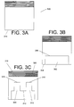
- FIGS. 1A through 1H illustrate, in simplified form, one example approach of the "trench” technique not according to the invention
- FIG. 2 illustrates, in simplified form, a wafer using one example approach as described herein;
- FIGS. 3A through 3L illustrate a variant of the aforementioned approach according to the invention involving two or more "stacked" trenches.
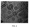
- FIG. 4 is a photograph of a portion of a wafer created using one of the approaches described herein.
- Our approach is a "trench" technique that involves first etching regions of the backside of the fully formed wafer to allow the wafer to be thin in those regions where it needs to be for deep via formation while allowing proper seed deposition, while a large portion of the wafer is maintained either at full thickness or some pre-thinned thickness that still maintains the wafer at a thickness and overall rigidity that will allow it to be further handled in a routine manner.
- the thinned regions can:
- a reduced area For purposes of consistency, such a reduced area will be referred to herein as a "trench" with the understanding that the term is not intended to incorporate any particular shape, aspect (i.e. depth to width) relationship or other geometric configuration.
- these trenches can be created so that they can assist in some later-performed step as will be described in greater detail below.
- the total area of the trenches relative as a fraction of the overall area of the wafer should typically be under 75% and typically 50% or less to ensure the structural integrity of the wafer and ability for it to be handled in a conventional manner is maintained.
- trench formation can be done with the same etch processes used for forming the vias.
- the trench(es) can be formed using a lower-precision process like a wet-etch process.
- the trench depth can be greater or lesser depending upon the via diameter and depth.
- the trench depth needed is one that will allow for a via that is formed into the wafer within the trench to be seeded to its complete depth.
- a wafer with an overall thickness of 750um would only require a trench that would render the wafer 400um thick in the required area if 50um diameter vias were to be created. or a trench to render the wafer 150um thick if 10um diameter vias were to be made.
- deeper trenches i.e. thinner wafer regions
- a multi-stepped approach is used in which two or more "stacked trenches" are used to bring the wafer down to the necessary reduced thickness while maintaining the overall structural integrity.
- FIGS. 1A through 1G illustrate, in simplified form, one example approach of the "trench” techniques, which is not according to the invention.
- FIG 1A illustrates, in simplified form, a part of a semiconductor wafer 100.
- the semiconductor is full thickness and ready for dicing, in that both front end and backend processing are complete.
- the wafer will also be processed to add vias from the back side down to some portion of one of the layers of metalization placed as part of the backend processing.
- a trench 102 is formed over the area where the deep metal filled vias will be, but the wafer is too thick to allow for either via etching down to the depth required, seed deposition or both.
- the trench area 104 is defined and formed using, for example, a conventional dry etch or wet etch approach down to a depth 106 sufficient to define a new outer surface 108, of sufficient distance from (in this example) the metalization point 110 that will be connected to, and to meet the criteria necessary for via creation and seed deposition down to that metalization point 110.
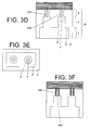
- the surface shape of the trench 102 is limited only by the ability to define it. Thus, depending upon the particular application, any shape from a simple quadrilateral or circular shape to a highly complex geometric shape can be used.
- the via is formed in the desired manner.
- an annular via approach such as described in the above-referenced patent applications is used.
- the via 110, 112 within the trench 102 are shown.
- the via 110 on the left will extend to an intermediate point 110 in the metalization layers, whereas the via 112 on the right will only extend to the first metalization layer 116.
- the vias 110, 112 are of different depths, they would not be formed at the same time, but rather, vias of a common depth would be created at the same time if they had the same diameter.
- the annular vias 110, 112 are not in any way shown to scale and, in fact all proportions are grossly exaggerated and out of scale.
- an annular ring shaped via trench 118 is formed.
- the via trench 118 is filled with an insulator 120.
- the inner island of semiconductor material 122 within the insulator 120 is removed.
- a seed layer 124 is deposited and the via filled with metal 126 using, in this example, an electroplating process. Thereafter, any additional desired processing steps, such as formation of device pads or other acts not relevant to understanding the process, are performed.
- the wafer will either simply be sawn or diced (for the former case) or it can now be thinned to provide access to the contacts 128, 130 formed by the metal-filled vias and then diced or sawn.
- the newly formed vias can be used as posts 132, 134, in other implementation variants, the vias can have contact pads 128, 130 attached to them.
- FIG. 2 illustrates, in simplified form, a wafer 200 using one example approach as described herein, both from the trench side ( FIG. 2A ) and, in cross section taken at A-A ( FIG. 2B ).
- the trenches 202 are sized and shaped so as to be aligned with, and slightly larger than, the individual chips 204 formed on the wafer 200.
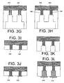
- FIGS. 3A through 3L illustrate a variant of the aforementioned approach according to the invention involving two or more "stacked" trenches to accommodate, for example, extremely narrow vias in a thick wafer or specific contact formation requirements.
- this approach begins with a fully formed wafer 300, a simplified portion of which is shown in FIG. 3A .
- a trench 302 is formed in the back side 304 of the wafer 300 down to a specified depth 306, again using, for example, a wet or dry etch approach.
- a pair of smaller trenches 308, 310 are formed in the bottom surface 312 of the first trench 302 in the same way as the first trench 302 was formed.
- the "same way” merely means that the lower surface 312 of the first trench 302is treated as a starting surface (i.e. like the original surface 314 of the wafer 300 before the first trench 302 was formed). It is not intended to imply that the identical approach used to form the first trench must be used - the same or a different approach could be used.
- the distance between the bottom surface 316 of the secondary trenches 308, 310 and the desired connection points 318, 320 will be within the necessary range to allow for seed deposit with the intended via sizing.
- annular via 322, 324 is created that extends from the bottom 316 of the secondary trench 308, 310 to the respective desired connection points 318, 320, here again, a respective point in the metalization layers.
- FIG. 3E illustrates a view of the portion of the wafer 300 taken from the trench side.
- FIG. 3E therefore, provides an alternate view of surfaces "a", “b", and “c” and the annular trench "d".
- FIG. 3F shows the wafer 300 after the annular vias 322, 324 have been filled with an insulator 326.
- FIG. 3G shows the wafer 300 after the island 328 of semiconductor material within the annular insulator 326 has been removed down to the desired metalization connection point 318, 320.
- FIG. 3H shows the wafer 300 after the void has been seeded 342 and filled with metal 344.
- the wafer 300 can be diced and the chips, can be thinned to expose the newly formed contacts 346, 348, or the wafer 300 can be thinned before dicing - in either case followed by, for example, creation of contact pads 330, 332 if desired or necessary ( FIG. 3J ).
- the wafer or chip if diced was related to the point to be connected to as opposed to the overall via pitch and the secondary trenches were appropriately sized and spaced
- the wafer or chip if diced) could be thinned down simply to the secondary trenches ( FIG. 3K ). Thereafter, the secondary trenches could themselves be filled with a conductor 334, such as shown in FIG. 3L , before, or as part of, a contact pad formation process. In this manner, greater wafer or chip thickness can be maintained.
- FIG. 4 is a photograph of a portion of a wafer created using one of the above approaches. As can be seen, in the approach of FIG. 4 , multiple trenches are used within the boundaries of a single chip, in this case on an individual via basis.
- the trenches can be formed so as to serve other purposes as well.
- the trenches can be designed to help channel insulator into an annular trench or to confine metal that will become or otherwise form a rerouting trace.
- the trenches can advantageously serve multiple purposes beyond merely addressing the via depth problem noted above.
Landscapes
- Engineering & Computer Science (AREA)
- Physics & Mathematics (AREA)
- Condensed Matter Physics & Semiconductors (AREA)
- General Physics & Mathematics (AREA)
- Computer Hardware Design (AREA)
- Microelectronics & Electronic Packaging (AREA)
- Power Engineering (AREA)
- Manufacturing & Machinery (AREA)
- Internal Circuitry In Semiconductor Integrated Circuit Devices (AREA)
- Electroplating Methods And Accessories (AREA)
Description
- When working with semiconductor wafers, it is desirable to handle thick wafers to ensure they do not break during processing. However, the deeper the via, the harder it is to get a seed layer into it using currently available deposition techniques and equipment, particularly if cost is a consideration. Typically, applying a seed layer to a depth of more than 150um in a narrow via is generally difficult and cost-ineffective. Thus, it is difficult to use the vias of the aforementioned patent applications on a wafer while maintaining the typically about 500 to 750um (or thicker) thickness that is common to most commercially available wafers, without first thinning them, if a plating approach to filling the narrow width vias will be used. However, thinning such wafers to the appropriate thickness can render the wafers flexible but, because they are brittle, significantly likely to break during handling. While this may be an acceptable risk for a pre-processed wafer, where the cost is minimal, it is not acceptable for a fully processed wafer (i.e. one that already has undergone at least its front end processing, and in many cases its backend processing as well) because the cost is significantly higher.
-
US 2006/0042952 Al discloses a method of forming an electrically-conductive via in a wafer by forming a trench in a backside of the wafer to a dirst depth and forming a via in the backside of the wafer, the first via extending from a surface of the trench into the backside of the wafer to a second depth and filling the via with a seed layer and a conductive material and thinning the backside of the wafer down to the via. - We have devised a way to overcome the above problem in a manner that allows the above-referenced vias to be used on fully processed wafers without having to thin the wafer down to fragile thicknesses. Moreover, our approach does not require the use of extremely high precision or high cost techniques to do so.
- In our approach, the thickness of only select portions of the wafer will be reduced. In this manner, within the reduced areas, the thickness is such that the above-referenced via approaches can be used and an appropriate seed layer can be deposited. Moreover, because the only portions of the area are reduced, the overall structural rigidity of the wafer can be retained to the extent necessary to allow for the necessary handling. Still further, regions where the thickness is to be reduced can be limited to areas where vias are to be located and can be etched in large fashion using coarse etching techniques if desired because the boundaries are not critical. In fact, in some cases, post via-formation thinning will remove the boundaries entirely.
- The present invention provides a method as recited in the claims.
- The advantages and features described herein are a few of the many advantages and features available from representative embodiments and are presented only to assist in understanding the invention. It should be understood that they are not to be considered limitations on the invention or limitations on equivalents. For instance, some of these advantages are mutually contradictory, in that they cannot be simultaneously present in a single embodiment. Similarly, some advantages are applicable to one aspect of the invention, and inapplicable to others. Additional features and advantages will become apparent in the following description and the drawings.
-
FIGS. 1A through 1H illustrate, in simplified form, one example approach of the "trench" technique not according to the invention; -
FIG. 2 illustrates, in simplified form, a wafer using one example approach as described herein; -
FIGS. 3A through 3L illustrate a variant of the aforementioned approach according to the invention involving two or more "stacked" trenches; and -
FIG. 4 is a photograph of a portion of a wafer created using one of the approaches described herein. -
U.S. Patent Applications, Serial Nos. 11/329,481 ,11/329,506 11/329,539 11/329,540 11/329,556 11/329,557 11/329,558 11/329,574 11/329,575 11/329,576 11/329,873 11/329,874 11/329,875 11/329,883 11/329,885 11/329,886 11/329,887 11/329,952 11/329,953 11/329,955 11/330,011 11/422,551 - Our techniques described in those applications allow for via densities and placement that was previously unachievable and can be performed on a chip, die or wafer scale. In some cases, it is desirable to perform the techniques on a wafer that already has had its devices formed, and its backend processing (i.e. formation of inter-device, interconnect metalization layers) completed, or on a wafer that has not been pre-thinned. Typical semiconductor wafers are typically about 500um to 750um or greater in thickness.
- However, as noted above, with wafers of that thickness, it is extremely difficult to create numerous, small densely packed vias that can extend down to device contacts or one or more of the backend metalization layers and can be seeded so that they can be metalized. The approaches described in the above-referenced patent applications generally avoid the issue by pre-thinning the wafer before via formation, if a wafer scale approach is to be used. However, as noted above, thinning the full wafer beyond a certain amount causes it to become too fragile to be handled using routine wafer processing approaches.
- Our approach is a "trench" technique that involves first etching regions of the backside of the fully formed wafer to allow the wafer to be thin in those regions where it needs to be for deep via formation while allowing proper seed deposition, while a large portion of the wafer is maintained either at full thickness or some pre-thinned thickness that still maintains the wafer at a thickness and overall rigidity that will allow it to be further handled in a routine manner.
- Depending upon the particular implementation, the thinned regions can:
- i) cover an area equal to or exceeding the area of an individual chip as it will exist once diced;
- ii) cover smaller areas where groups of vias will be formed; or
- iii) cover only those individual areas where individual vias will be formed.
- For purposes of consistency, such a reduced area will be referred to herein as a "trench" with the understanding that the term is not intended to incorporate any particular shape, aspect (i.e. depth to width) relationship or other geometric configuration.
- Moreover, these trenches can be created so that they can assist in some later-performed step as will be described in greater detail below.
- Irrespective of the which of the above three approaches are used, the total area of the trenches relative as a fraction of the overall area of the wafer should typically be under 75% and typically 50% or less to ensure the structural integrity of the wafer and ability for it to be handled in a conventional manner is maintained.
- Advantageously, trench formation can be done with the same etch processes used for forming the vias. Alternatively, the trench(es) can be formed using a lower-precision process like a wet-etch process.
- Still further, the trench depth can be greater or lesser depending upon the via diameter and depth. Notably, the trench depth needed is one that will allow for a via that is formed into the wafer within the trench to be seeded to its complete depth. For example, a wafer with an overall thickness of 750um, would only require a trench that would render the wafer 400um thick in the required area if 50um diameter vias were to be created. or a trench to render the wafer 150um thick if 10um diameter vias were to be made. As noted above, deeper trenches (i.e. thinner wafer regions) can also be accommodated, although the thinner the wafer within the trench, the greater the remaining area of wafer that must be left.
- In cases according to the invention, typically those with the narrowest diameter vias, a multi-stepped approach is used in which two or more "stacked trenches" are used to bring the wafer down to the necessary reduced thickness while maintaining the overall structural integrity.
- Finally, while the approach is illustratively described with respect to vias such as described in the above referenced, commonly assigned, patent applications, the same approach can be used with other via formation techniques that have similar issues.
- Turning now to the figures,
FIGS. 1A through 1G illustrate, in simplified form, one example approach of the "trench" techniques, which is not according to the invention. -
FIG 1A illustrates, in simplified form, a part of asemiconductor wafer 100. As shown, the semiconductor is full thickness and ready for dicing, in that both front end and backend processing are complete. However, for purposes of this example, we presume that the wafer will also be processed to add vias from the back side down to some portion of one of the layers of metalization placed as part of the backend processing. - The process proceeds as follows.
- First, as shown in
FIG. 1B , atrench 102 is formed over the area where the deep metal filled vias will be, but the wafer is too thick to allow for either via etching down to the depth required, seed deposition or both. Thetrench area 104 is defined and formed using, for example, a conventional dry etch or wet etch approach down to adepth 106 sufficient to define a newouter surface 108, of sufficient distance from (in this example) themetalization point 110 that will be connected to, and to meet the criteria necessary for via creation and seed deposition down to thatmetalization point 110. - Note that the surface shape of the
trench 102 is limited only by the ability to define it. Thus, depending upon the particular application, any shape from a simple quadrilateral or circular shape to a highly complex geometric shape can be used. - Next, the via is formed in the desired manner. As shown in
FIGS. 1C through FIG. 1G , for purposes of illustration, an annular via approach such as described in the above-referenced patent applications is used. - For purposes of illustration and simplicity, two
vias trench 102 are shown. For purposes of understanding, the via 110 on the left will extend to anintermediate point 110 in the metalization layers, whereas the via 112 on the right will only extend to thefirst metalization layer 116. However, it should be understood that, because thevias annular vias - Returning to the Figures, as shown in
FIG. 1C , an annular ring shaped viatrench 118 is formed. As shown inFIG. 1D , the viatrench 118 is filled with aninsulator 120. As shown inFIG. 1E , the inner island ofsemiconductor material 122 within theinsulator 120 is removed. As shown inFIG. 1F , aseed layer 124 is deposited and the via filled withmetal 126 using, in this example, an electroplating process. Thereafter, any additional desired processing steps, such as formation of device pads or other acts not relevant to understanding the process, are performed. - Finally, as shown in
FIG. 1G and 1H , depending upon the extent of the trench used (i.e. if it was a single trench exceeding the boundaries of the chip or not) the wafer will either simply be sawn or diced (for the former case) or it can now be thinned to provide access to thecontacts posts contact pads - Note that, although the approach was illustrated for a pair of vias, the approach would be the same for a single via or for multiple vias (from two to literally hundreds or more), the only difference being the size or shape of the trench that would be used.
-
FIG. 2 illustrates, in simplified form, awafer 200 using one example approach as described herein, both from the trench side (FIG. 2A ) and, in cross section taken at A-A (FIG. 2B ). With this approach, the trenches 202 are sized and shaped so as to be aligned with, and slightly larger than, theindividual chips 204 formed on thewafer 200. -
FIGS. 3A through 3L illustrate a variant of the aforementioned approach according to the invention involving two or more "stacked" trenches to accommodate, for example, extremely narrow vias in a thick wafer or specific contact formation requirements. - As with the above approach, this approach begins with a fully formed
wafer 300, a simplified portion of which is shown inFIG. 3A . - As shown in
FIG. 3B , atrench 302 is formed in theback side 304 of thewafer 300 down to a specifieddepth 306, again using, for example, a wet or dry etch approach. - Next, as shown in
FIG. 3C , a pair ofsmaller trenches bottom surface 312 of thefirst trench 302 in the same way as thefirst trench 302 was formed. To avoid confusion, note that the "same way" merely means that thelower surface 312 of the first trench 302is treated as a starting surface (i.e. like theoriginal surface 314 of thewafer 300 before thefirst trench 302 was formed). It is not intended to imply that the identical approach used to form the first trench must be used - the same or a different approach could be used. - After formation of the
secondary depth trenches bottom surface 316 of thesecondary trenches - Now, the actual via formation process can begin and, for purposes of example and simplicity, the basic annular via approach is used (bearing in mind that, as above, dimensions are not to scale). Thus, as shown in
FIG. 3D , an annular via 322, 324 is created that extends from thebottom 316 of thesecondary trench - At this point it should be noted that, even though two
different trenches original surface 314 toconnection point 318 thickness N. Moreover, an even greater portion of thewafer 300 remains at a thickness of N - Z and only a small portion of the wafer is at a thickness of N - (Y + Z). Still further, using this multi-depth (or multiple stepped) approach, a flexibility in selecting the depths Y and Z is available without significant risk of weakening the wafer. -
FIG. 3E illustrates a view of the portion of thewafer 300 taken from the trench side.FIG. 3E , therefore, provides an alternate view of surfaces "a", "b", and "c" and the annular trench "d". -
FIG. 3F shows thewafer 300 after theannular vias insulator 326.FIG. 3G shows thewafer 300 after theisland 328 of semiconductor material within theannular insulator 326 has been removed down to the desiredmetalization connection point FIG. 3H shows thewafer 300 after the void has been seeded 342 and filled withmetal 344. - At this point, with this approach, two new options become available. With one option, as shown in
FIG. 3I , thewafer 300 can be diced and the chips, can be thinned to expose the newly formedcontacts wafer 300 can be thinned before dicing - in either case followed by, for example, creation ofcontact pads FIG. 3J ). With the other option, if, for example, the reason for the need for very narrow vias was related to the point to be connected to as opposed to the overall via pitch and the secondary trenches were appropriately sized and spaced, the wafer or chip (if diced) could be thinned down simply to the secondary trenches (FIG. 3K ). Thereafter, the secondary trenches could themselves be filled with aconductor 334, such as shown inFIG. 3L , before, or as part of, a contact pad formation process. In this manner, greater wafer or chip thickness can be maintained. -
FIG. 4 is a photograph of a portion of a wafer created using one of the above approaches. As can be seen, in the approach ofFIG. 4 , multiple trenches are used within the boundaries of a single chip, in this case on an individual via basis. - Finally, it is worth noting that, in some variants, the trenches can be formed so as to serve other purposes as well. For example, in various implementations, the trenches can be designed to help channel insulator into an annular trench or to confine metal that will become or otherwise form a rerouting trace. Thus, depending upon the particular implementation and configuration, the trenches can advantageously serve multiple purposes beyond merely addressing the via depth problem noted above.
- It should thus be understood that this description (including the figures) is only representative of some illustrative embodiments. For the convenience of the reader, the above description has focused on a representative sample of all possible embodiments, a sample that teaches the principles of the invention. The description has not attempted to exhaustively enumerate all possible variations. That alternate embodiments may not have been presented for a specific portion of the invention, or that further undescribed alternate embodiments may be available for a portion, is not to be considered a disclaimer of those alternate embodiments. One of ordinary skill will appreciate that many of those undescribed embodiments incorporate the same principles of the invention and others are equivalent.
Claims (9)
- A method of forming an electrically-conductive via (322;324) in a processed wafer (300), the method comprising:forming a first trench (302) in a backside of the processed wafer (300) to a first depth (306);forming a second trench (308;310) having a cross-sectional area into a bottom surface (312) of the first trench (302);forming a first via (322;324) extending from a bottom surface (316) of the second trench (308;310) into the backside of the processed wafer (300) to a second depth, wherein the first via (322;324) has a cross-sectional area that is smaller than the cross-sectional area of the second trench (308:310);depositing a seed layer (342) over a full length of the first via (322);plating the seed layer to fill the first via (322;324) with an electrically-conductive metal (344);thinning the backside of the processed wafer (300) down to the second trench (308;310); anddepositing a conductor (334) within the second trench (308;310) after said thinning the backside of the processed wafer (300).
- The method of claim 1, wherein at least one of said forming a first trench (302) or forming a second trench (308;310) comprises etching the backside of the processed wafer (300) using at least one of a wet etch or a dry etch process.
- The method of claim 1, further comprising forming a plurality of trenches into the backside (304) of the processed wafer (300), wherein the plurality of trenches define a trench area, and wherein the trench area is less than 75 percent of an overall area of the backside (304) of the processed wafer (300).
- The method of claim 3, wherein the trench area is less than 50 percent of the overall area of the backside (304) of the processed wafer (300).
- The method of claim 1, wherein said forming a first trench (302) and said forming a second trench (308;310) comprise forming a stepped trench (302,308).
- The method of claim 1, wherein the processed wafer (300) comprises multiple chips, the method further comprising defining a periphery for a trench area that exceeds an outer boundary of one or more of the multiple chips.
- The method of claim 1, wherein the processed wafer (300) comprises multiple chips, the method further comprising defining a periphery for a trench area that is at least partially within an outer boundary of one of the multiple chips.
- The method of claim 1, wherein the processed wafer (300) comprises multiple chips, the method further comprising defining a trench area that is substantially aligned with one of the multiple chips, wherein the trench area has a size slightly larger than the one of the multiple chips.
- The method of claim 1, further comprising sawing or dicing a chip from the processed wafer (300).
Applications Claiming Priority (2)
| Application Number | Priority Date | Filing Date | Title |
|---|---|---|---|
| US82977206P | 2006-10-17 | 2006-10-17 | |
| PCT/US2007/081380 WO2008048925A2 (en) | 2006-10-17 | 2007-10-15 | Wafer via formation |
Publications (3)
| Publication Number | Publication Date |
|---|---|
| EP2074647A2 EP2074647A2 (en) | 2009-07-01 |
| EP2074647A4 EP2074647A4 (en) | 2010-07-28 |
| EP2074647B1 true EP2074647B1 (en) | 2012-10-10 |
Family
ID=39314773
Family Applications (1)
| Application Number | Title | Priority Date | Filing Date |
|---|---|---|---|
| EP07844296A Active EP2074647B1 (en) | 2006-10-17 | 2007-10-15 | Wafer via formation |
Country Status (6)
| Country | Link |
|---|---|
| US (1) | US7871927B2 (en) |
| EP (1) | EP2074647B1 (en) |
| JP (1) | JP5269799B2 (en) |
| KR (1) | KR101175393B1 (en) |
| CN (1) | CN101553903B (en) |
| WO (1) | WO2008048925A2 (en) |
Families Citing this family (7)
| Publication number | Priority date | Publication date | Assignee | Title |
|---|---|---|---|---|
| CN101916754B (en) * | 2010-06-29 | 2012-08-29 | 香港应用科技研究院有限公司 | Through-hole, through-hole forming method and through-hole filling method |
| WO2012119333A1 (en) * | 2011-03-04 | 2012-09-13 | 中国科学院微电子研究所 | Through-silicon-via (tsv) structure and its fabricating method |
| US8486805B2 (en) * | 2011-03-04 | 2013-07-16 | Institute of Microelectronics, Chinese Academy of Sciences | Through-silicon via and method for forming the same |
| CN102683308B (en) * | 2011-03-11 | 2015-02-04 | 中国科学院微电子研究所 | Through-silicon-vias structure and formation method thereof |
| US20130015504A1 (en) * | 2011-07-11 | 2013-01-17 | Chien-Li Kuo | Tsv structure and method for forming the same |
| JP5834563B2 (en) * | 2011-07-14 | 2015-12-24 | セイコーエプソン株式会社 | Manufacturing method of semiconductor device |
| US11398415B2 (en) * | 2018-09-19 | 2022-07-26 | Intel Corporation | Stacked through-silicon vias for multi-device packages |
Family Cites Families (82)
| Publication number | Priority date | Publication date | Assignee | Title |
|---|---|---|---|---|
| US3312878A (en) | 1965-06-01 | 1967-04-04 | Ibm | High speed packaging of miniaturized circuit modules |
| JPH02257643A (en) | 1989-03-29 | 1990-10-18 | Mitsubishi Electric Corp | Semiconductor device and its manufacture |
| US5075253A (en) * | 1989-04-12 | 1991-12-24 | Advanced Micro Devices, Inc. | Method of coplanar integration of semiconductor IC devices |
| US5399898A (en) | 1992-07-17 | 1995-03-21 | Lsi Logic Corporation | Multi-chip semiconductor arrangements using flip chip dies |
| JPH0831617B2 (en) | 1990-04-18 | 1996-03-27 | 三菱電機株式会社 | Solar cell and manufacturing method thereof |
| JP2918307B2 (en) | 1990-08-07 | 1999-07-12 | 沖電気工業株式会社 | Semiconductor storage element |
| KR940006696B1 (en) | 1991-01-16 | 1994-07-25 | 금성일렉트론 주식회사 | Manufacturing method of isolation layer of semiconductor device |
| EP0516866A1 (en) | 1991-05-03 | 1992-12-09 | International Business Machines Corporation | Modular multilayer interwiring structure |
| US5308784A (en) | 1991-10-02 | 1994-05-03 | Samsung Electronics Co., Ltd. | Semiconductor device and method for making the same |
| US5603847A (en) | 1993-04-07 | 1997-02-18 | Zycon Corporation | Annular circuit components coupled with printed circuit board through-hole |
| JPH0897375A (en) * | 1994-07-26 | 1996-04-12 | Toshiba Corp | Microwave integrated circuit device and manufacture thereof |
| US5587119A (en) | 1994-09-14 | 1996-12-24 | E-Systems, Inc. | Method for manufacturing a coaxial interconnect |
| DE4433845A1 (en) | 1994-09-22 | 1996-03-28 | Fraunhofer Ges Forschung | Method of manufacturing a three-dimensional integrated circuit |
| US5814889A (en) | 1995-06-05 | 1998-09-29 | Harris Corporation | Intergrated circuit with coaxial isolation and method |
| US5608264A (en) | 1995-06-05 | 1997-03-04 | Harris Corporation | Surface mountable integrated circuit with conductive vias |
| US5872051A (en) | 1995-08-02 | 1999-02-16 | International Business Machines Corporation | Process for transferring material to semiconductor chip conductive pads using a transfer substrate |
| JP2739855B2 (en) | 1995-12-14 | 1998-04-15 | 日本電気株式会社 | Semiconductor device and manufacturing method thereof |
| US5973396A (en) | 1996-02-16 | 1999-10-26 | Micron Technology, Inc. | Surface mount IC using silicon vias in an area array format or same size as die array |
| US6310484B1 (en) | 1996-04-01 | 2001-10-30 | Micron Technology, Inc. | Semiconductor test interconnect with variable flexure contacts |
| US5872338A (en) | 1996-04-10 | 1999-02-16 | Prolinx Labs Corporation | Multilayer board having insulating isolation rings |
| JP2790122B2 (en) | 1996-05-31 | 1998-08-27 | 日本電気株式会社 | Laminated circuit board |
| US7052941B2 (en) | 2003-06-24 | 2006-05-30 | Sang-Yun Lee | Method for making a three-dimensional integrated circuit structure |
| JP3176307B2 (en) | 1997-03-03 | 2001-06-18 | 日本電気株式会社 | Mounting structure of integrated circuit device and method of manufacturing the same |
| JP3724110B2 (en) * | 1997-04-24 | 2005-12-07 | 三菱電機株式会社 | Manufacturing method of semiconductor device |
| JPH10335383A (en) | 1997-05-28 | 1998-12-18 | Matsushita Electric Ind Co Ltd | Producing method for semiconductor device |
| JPH11166935A (en) | 1997-09-25 | 1999-06-22 | Canon Inc | Light probe for light detection or irradiation, near-field optical microscope provided with the probe, manufacture of the light probe and substrate used for its manufacture |
| US6013551A (en) * | 1997-09-26 | 2000-01-11 | Taiwan Semiconductor Manufacturing Company, Ltd. | Method of manufacture of self-aligned floating gate, flash memory cell and device manufactured thereby |
| US6620731B1 (en) | 1997-12-18 | 2003-09-16 | Micron Technology, Inc. | Method for fabricating semiconductor components and interconnects with contacts on opposing sides |
| US6075710A (en) | 1998-02-11 | 2000-06-13 | Express Packaging Systems, Inc. | Low-cost surface-mount compatible land-grid array (LGA) chip scale package (CSP) for packaging solder-bumped flip chips |
| US5962922A (en) | 1998-03-18 | 1999-10-05 | Wang; Bily | Cavity grid array integrated circuit package |
| US6222276B1 (en) | 1998-04-07 | 2001-04-24 | International Business Machines Corporation | Through-chip conductors for low inductance chip-to-chip integration and off-chip connections |
| US6380023B2 (en) | 1998-09-02 | 2002-04-30 | Micron Technology, Inc. | Methods of forming contacts, methods of contacting lines, methods of operating integrated circuitry, and integrated circuits |
| US6122187A (en) | 1998-11-23 | 2000-09-19 | Micron Technology, Inc. | Stacked integrated circuits |
| US6330145B1 (en) * | 1998-12-30 | 2001-12-11 | Stmicroelectronics, Inc. | Apparatus and method for contacting a sensor conductive layer |
| US6316737B1 (en) | 1999-09-09 | 2001-11-13 | Vlt Corporation | Making a connection between a component and a circuit board |
| JP3386029B2 (en) | 2000-02-09 | 2003-03-10 | 日本電気株式会社 | Flip chip type semiconductor device and manufacturing method thereof |
| US6498387B1 (en) * | 2000-02-15 | 2002-12-24 | Wen-Ken Yang | Wafer level package and the process of the same |
| US6446317B1 (en) | 2000-03-31 | 2002-09-10 | Intel Corporation | Hybrid capacitor and method of fabrication therefor |
| JP2001338947A (en) | 2000-05-26 | 2001-12-07 | Nec Corp | Flip chip type semiconductor device and its manufacturing method |
| TW525417B (en) | 2000-08-11 | 2003-03-21 | Ind Tech Res Inst | Composite through hole structure |
| US6577013B1 (en) | 2000-09-05 | 2003-06-10 | Amkor Technology, Inc. | Chip size semiconductor packages with stacked dies |
| US6720245B2 (en) | 2000-09-07 | 2004-04-13 | Interuniversitair Microelektronica Centrum (Imec) | Method of fabrication and device for electromagnetic-shielding structures in a damascene-based interconnect scheme |
| US6740576B1 (en) | 2000-10-13 | 2004-05-25 | Bridge Semiconductor Corporation | Method of making a contact terminal with a plated metal peripheral sidewall portion for a semiconductor chip assembly |
| JP2002134545A (en) | 2000-10-26 | 2002-05-10 | Oki Electric Ind Co Ltd | Semiconductor integrated circuit chip, board and their manufacturing method |
| JP4608763B2 (en) | 2000-11-09 | 2011-01-12 | 日本電気株式会社 | Semiconductor device |
| EP1217656A1 (en) | 2000-12-20 | 2002-06-26 | STMicroelectronics S.r.l. | Process for manufacturing components in a semiconductor material with reduction in the starting wafer thickness |
| US6512300B2 (en) | 2001-01-10 | 2003-01-28 | Raytheon Company | Water level interconnection |
| JP4118029B2 (en) | 2001-03-09 | 2008-07-16 | 富士通株式会社 | Semiconductor integrated circuit device and manufacturing method thereof |
| US6753199B2 (en) | 2001-06-29 | 2004-06-22 | Xanoptix, Inc. | Topside active optical device apparatus and method |
| TW567554B (en) * | 2001-08-08 | 2003-12-21 | Lam Res Corp | All dual damascene oxide etch process steps in one confined plasma chamber |
| US7218349B2 (en) | 2001-08-09 | 2007-05-15 | Semiconductor Energy Laboratory Co., Ltd. | Semiconductor device |
| US6747347B2 (en) | 2001-08-30 | 2004-06-08 | Micron Technology, Inc. | Multi-chip electronic package and cooling system |
| JP3495727B2 (en) | 2001-11-07 | 2004-02-09 | 新光電気工業株式会社 | Semiconductor package and manufacturing method thereof |
| US6599778B2 (en) | 2001-12-19 | 2003-07-29 | International Business Machines Corporation | Chip and wafer integration process using vertical connections |
| US6590278B1 (en) | 2002-01-08 | 2003-07-08 | International Business Machines Corporation | Electronic package |
| US6762076B2 (en) * | 2002-02-20 | 2004-07-13 | Intel Corporation | Process of vertically stacking multiple wafers supporting different active integrated circuit (IC) devices |
| US6770822B2 (en) | 2002-02-22 | 2004-08-03 | Bridgewave Communications, Inc. | High frequency device packages and methods |
| US20030183943A1 (en) * | 2002-03-28 | 2003-10-02 | Swan Johanna M. | Integrated circuit die and an electronic assembly having a three-dimensional interconnection scheme |
| JP2003318178A (en) | 2002-04-24 | 2003-11-07 | Seiko Epson Corp | Semiconductor device, its manufacturing method, circuit board, and electronic apparatus |
| US7135777B2 (en) | 2002-05-03 | 2006-11-14 | Georgia Tech Research Corporation | Devices having compliant wafer-level input/output interconnections and packages using pillars and methods of fabrication thereof |
| US6939789B2 (en) | 2002-05-13 | 2005-09-06 | Taiwan Semiconductor Manufacturing Co., Ltd. | Method of wafer level chip scale packaging |
| SG142115A1 (en) * | 2002-06-14 | 2008-05-28 | Micron Technology Inc | Wafer level packaging |
| SG111069A1 (en) | 2002-06-18 | 2005-05-30 | Micron Technology Inc | Semiconductor devices including peripherally located bond pads, assemblies, packages, and methods |
| JP3679786B2 (en) | 2002-06-25 | 2005-08-03 | 松下電器産業株式会社 | Manufacturing method of semiconductor device |
| US6887792B2 (en) * | 2002-09-17 | 2005-05-03 | Hewlett-Packard Development Company, L.P. | Embossed mask lithography |
| SG111972A1 (en) | 2002-10-17 | 2005-06-29 | Agency Science Tech & Res | Wafer-level package for micro-electro-mechanical systems |
| US6790775B2 (en) * | 2002-10-31 | 2004-09-14 | Hewlett-Packard Development Company, L.P. | Method of forming a through-substrate interconnect |
| KR100482179B1 (en) * | 2002-12-16 | 2005-04-14 | 동부아남반도체 주식회사 | Fabricating method of semiconductor device |
| ITTO20030269A1 (en) | 2003-04-08 | 2004-10-09 | St Microelectronics Srl | PROCEDURE FOR THE MANUFACTURE OF A DEVICE |
| US20050046034A1 (en) | 2003-09-03 | 2005-03-03 | Micron Technology, Inc. | Apparatus and method for high density multi-chip structures |
| US6897125B2 (en) * | 2003-09-17 | 2005-05-24 | Intel Corporation | Methods of forming backside connections on a wafer stack |
| TWI251313B (en) | 2003-09-26 | 2006-03-11 | Seiko Epson Corp | Intermediate chip module, semiconductor device, circuit board, and electronic device |
| US20050104027A1 (en) | 2003-10-17 | 2005-05-19 | Lazarev Pavel I. | Three-dimensional integrated circuit with integrated heat sinks |
| US7276787B2 (en) | 2003-12-05 | 2007-10-02 | International Business Machines Corporation | Silicon chip carrier with conductive through-vias and method for fabricating same |
| US7230318B2 (en) | 2003-12-24 | 2007-06-12 | Agency For Science, Technology And Research | RF and MMIC stackable micro-modules |
| US7425499B2 (en) * | 2004-08-24 | 2008-09-16 | Micron Technology, Inc. | Methods for forming interconnects in vias and microelectronic workpieces including such interconnects |
| US7378342B2 (en) * | 2004-08-27 | 2008-05-27 | Micron Technology, Inc. | Methods for forming vias varying lateral dimensions |
| US7157310B2 (en) | 2004-09-01 | 2007-01-02 | Micron Technology, Inc. | Methods for packaging microfeature devices and microfeature devices formed by such methods |
| US7223654B2 (en) * | 2005-04-15 | 2007-05-29 | International Business Machines Corporation | MIM capacitor and method of fabricating same |
| US7531448B2 (en) * | 2005-06-22 | 2009-05-12 | United Microelectronics Corp. | Manufacturing method of dual damascene structure |
| US7750488B2 (en) * | 2006-07-10 | 2010-07-06 | Tezzaron Semiconductor, Inc. | Method for bonding wafers to produce stacked integrated circuits |
| US7531407B2 (en) * | 2006-07-18 | 2009-05-12 | International Business Machines Corporation | Semiconductor integrated circuit devices having high-Q wafer backside inductors and methods of fabricating same |
-
2007
- 2007-10-15 US US11/872,083 patent/US7871927B2/en not_active Expired - Fee Related
- 2007-10-15 JP JP2009533462A patent/JP5269799B2/en not_active Expired - Fee Related
- 2007-10-15 CN CN2007800375496A patent/CN101553903B/en not_active Expired - Fee Related
- 2007-10-15 EP EP07844296A patent/EP2074647B1/en active Active
- 2007-10-15 KR KR1020097007578A patent/KR101175393B1/en not_active IP Right Cessation
- 2007-10-15 WO PCT/US2007/081380 patent/WO2008048925A2/en active Application Filing
Also Published As
| Publication number | Publication date |
|---|---|
| EP2074647A4 (en) | 2010-07-28 |
| JP2010507260A (en) | 2010-03-04 |
| US7871927B2 (en) | 2011-01-18 |
| JP5269799B2 (en) | 2013-08-21 |
| CN101553903B (en) | 2012-08-29 |
| WO2008048925A2 (en) | 2008-04-24 |
| US20080090413A1 (en) | 2008-04-17 |
| EP2074647A2 (en) | 2009-07-01 |
| KR101175393B1 (en) | 2012-08-20 |
| CN101553903A (en) | 2009-10-07 |
| KR20090076914A (en) | 2009-07-13 |
| WO2008048925A3 (en) | 2008-07-03 |
Similar Documents
| Publication | Publication Date | Title |
|---|---|---|
| EP2074647B1 (en) | Wafer via formation | |
| US10741505B2 (en) | Method of manufacturing semiconductor device and semiconductor device | |
| EP2419930B1 (en) | Through substrate vias | |
| US9478480B2 (en) | Alignment mark and method of formation | |
| US7427803B2 (en) | Electromagnetic shielding using through-silicon vias | |
| US7510907B2 (en) | Through-wafer vias and surface metallization for coupling thereto | |
| US7867879B2 (en) | Method for dividing a semiconductor substrate and a method for producing a semiconductor circuit arrangement | |
| EP2831913B1 (en) | Method of providing a via hole and routing structure | |
| US8637967B2 (en) | Method for fabricating a semiconductor chip and semiconductor chip | |
| US7354799B2 (en) | Methods for anchoring a seal ring to a substrate using vias and assemblies including an anchored seal ring | |
| TW201222759A (en) | Semiconductor structure and process thereof | |
| JP2007005401A (en) | Semiconductor device and its manufacturing method | |
| CN103094170B (en) | For separating the method for multiple nude film and for separating the process equipment of multiple nude film | |
| US7871857B1 (en) | Methods of forming multi-chip semiconductor substrates | |
| US20050124140A1 (en) | Pre-fabrication scribing | |
| US8753982B2 (en) | Method for producing a connection region on a side wall of a semiconductor body | |
| JP2004349550A (en) | Semiconductor device and its manufacturing method | |
| US20240055309A1 (en) | Guard Ring Structure, Semiconductor Structure And Manufacturing Method | |
| CN115206880A (en) | Preparation method of GaN tube core | |
| EP1763079A1 (en) | Stackable semiconductor chip layer comprising prefabricated trench interconnect vias | |
| KR20230153271A (en) | Support structure to reinforce stacked semiconductor wafers | |
| KR20240023259A (en) | Method for manufacturing semiconductor device | |
| JP2002367932A (en) | Method for producing semiconductor device | |
| CN112997304A (en) | Semiconductor device with a plurality of semiconductor chips | |
| CN115424978A (en) | Semiconductor device and method for manufacturing the same |
Legal Events
| Date | Code | Title | Description |
|---|---|---|---|
| PUAI | Public reference made under article 153(3) epc to a published international application that has entered the european phase |
Free format text: ORIGINAL CODE: 0009012 |
|
| 17P | Request for examination filed |
Effective date: 20090414 |
|
| AK | Designated contracting states |
Kind code of ref document: A2 Designated state(s): AT BE BG CH CY CZ DE DK EE ES FI FR GB GR HU IE IS IT LI LT LU LV MC MT NL PL PT RO SE SI SK TR |
|
| AX | Request for extension of the european patent |
Extension state: AL BA HR MK RS |
|
| DAX | Request for extension of the european patent (deleted) | ||
| A4 | Supplementary search report drawn up and despatched |
Effective date: 20100630 |
|
| 17Q | First examination report despatched |
Effective date: 20110503 |
|
| REG | Reference to a national code |
Ref country code: DE Ref legal event code: R079 Ref document number: 602007026056 Country of ref document: DE Free format text: PREVIOUS MAIN CLASS: H01L0021300000 Ipc: H01L0021768000 |
|
| RIC1 | Information provided on ipc code assigned before grant |
Ipc: H01L 21/768 20060101AFI20120227BHEP |
|
| GRAP | Despatch of communication of intention to grant a patent |
Free format text: ORIGINAL CODE: EPIDOSNIGR1 |
|
| GRAS | Grant fee paid |
Free format text: ORIGINAL CODE: EPIDOSNIGR3 |
|
| GRAA | (expected) grant |
Free format text: ORIGINAL CODE: 0009210 |
|
| AK | Designated contracting states |
Kind code of ref document: B1 Designated state(s): AT BE BG CH CY CZ DE DK EE ES FI FR GB GR HU IE IS IT LI LT LU LV MC MT NL PL PT RO SE SI SK TR |
|
| REG | Reference to a national code |
Ref country code: GB Ref legal event code: FG4D |
|
| REG | Reference to a national code |
Ref country code: AT Ref legal event code: REF Ref document number: 579295 Country of ref document: AT Kind code of ref document: T Effective date: 20121015 Ref country code: CH Ref legal event code: EP |
|
| REG | Reference to a national code |
Ref country code: IE Ref legal event code: FG4D |
|
| REG | Reference to a national code |
Ref country code: DE Ref legal event code: R096 Ref document number: 602007026056 Country of ref document: DE Effective date: 20121206 |
|
| PG25 | Lapsed in a contracting state [announced via postgrant information from national office to epo] |
Ref country code: SI Free format text: LAPSE BECAUSE OF FAILURE TO SUBMIT A TRANSLATION OF THE DESCRIPTION OR TO PAY THE FEE WITHIN THE PRESCRIBED TIME-LIMIT Effective date: 20121010 |
|
| REG | Reference to a national code |
Ref country code: NL Ref legal event code: VDEP Effective date: 20121010 |
|
| REG | Reference to a national code |
Ref country code: AT Ref legal event code: MK05 Ref document number: 579295 Country of ref document: AT Kind code of ref document: T Effective date: 20121010 |
|
| REG | Reference to a national code |
Ref country code: LT Ref legal event code: MG4D |
|
| PG25 | Lapsed in a contracting state [announced via postgrant information from national office to epo] |
Ref country code: ES Free format text: LAPSE BECAUSE OF FAILURE TO SUBMIT A TRANSLATION OF THE DESCRIPTION OR TO PAY THE FEE WITHIN THE PRESCRIBED TIME-LIMIT Effective date: 20130121 Ref country code: FI Free format text: LAPSE BECAUSE OF FAILURE TO SUBMIT A TRANSLATION OF THE DESCRIPTION OR TO PAY THE FEE WITHIN THE PRESCRIBED TIME-LIMIT Effective date: 20121010 Ref country code: NL Free format text: LAPSE BECAUSE OF FAILURE TO SUBMIT A TRANSLATION OF THE DESCRIPTION OR TO PAY THE FEE WITHIN THE PRESCRIBED TIME-LIMIT Effective date: 20121010 Ref country code: SE Free format text: LAPSE BECAUSE OF FAILURE TO SUBMIT A TRANSLATION OF THE DESCRIPTION OR TO PAY THE FEE WITHIN THE PRESCRIBED TIME-LIMIT Effective date: 20121010 Ref country code: IS Free format text: LAPSE BECAUSE OF FAILURE TO SUBMIT A TRANSLATION OF THE DESCRIPTION OR TO PAY THE FEE WITHIN THE PRESCRIBED TIME-LIMIT Effective date: 20130210 Ref country code: LT Free format text: LAPSE BECAUSE OF FAILURE TO SUBMIT A TRANSLATION OF THE DESCRIPTION OR TO PAY THE FEE WITHIN THE PRESCRIBED TIME-LIMIT Effective date: 20121010 |
|
| PG25 | Lapsed in a contracting state [announced via postgrant information from national office to epo] |
Ref country code: BE Free format text: LAPSE BECAUSE OF FAILURE TO SUBMIT A TRANSLATION OF THE DESCRIPTION OR TO PAY THE FEE WITHIN THE PRESCRIBED TIME-LIMIT Effective date: 20121010 Ref country code: PT Free format text: LAPSE BECAUSE OF FAILURE TO SUBMIT A TRANSLATION OF THE DESCRIPTION OR TO PAY THE FEE WITHIN THE PRESCRIBED TIME-LIMIT Effective date: 20130211 Ref country code: MC Free format text: LAPSE BECAUSE OF NON-PAYMENT OF DUE FEES Effective date: 20121031 Ref country code: GR Free format text: LAPSE BECAUSE OF FAILURE TO SUBMIT A TRANSLATION OF THE DESCRIPTION OR TO PAY THE FEE WITHIN THE PRESCRIBED TIME-LIMIT Effective date: 20130111 Ref country code: LV Free format text: LAPSE BECAUSE OF FAILURE TO SUBMIT A TRANSLATION OF THE DESCRIPTION OR TO PAY THE FEE WITHIN THE PRESCRIBED TIME-LIMIT Effective date: 20121010 Ref country code: PL Free format text: LAPSE BECAUSE OF FAILURE TO SUBMIT A TRANSLATION OF THE DESCRIPTION OR TO PAY THE FEE WITHIN THE PRESCRIBED TIME-LIMIT Effective date: 20121010 |
|
| REG | Reference to a national code |
Ref country code: CH Ref legal event code: PL |
|
| PG25 | Lapsed in a contracting state [announced via postgrant information from national office to epo] |
Ref country code: AT Free format text: LAPSE BECAUSE OF FAILURE TO SUBMIT A TRANSLATION OF THE DESCRIPTION OR TO PAY THE FEE WITHIN THE PRESCRIBED TIME-LIMIT Effective date: 20121010 |
|
| REG | Reference to a national code |
Ref country code: IE Ref legal event code: MM4A |
|
| PG25 | Lapsed in a contracting state [announced via postgrant information from national office to epo] |
Ref country code: CH Free format text: LAPSE BECAUSE OF NON-PAYMENT OF DUE FEES Effective date: 20121031 Ref country code: LI Free format text: LAPSE BECAUSE OF NON-PAYMENT OF DUE FEES Effective date: 20121031 Ref country code: IE Free format text: LAPSE BECAUSE OF NON-PAYMENT OF DUE FEES Effective date: 20121015 Ref country code: BG Free format text: LAPSE BECAUSE OF FAILURE TO SUBMIT A TRANSLATION OF THE DESCRIPTION OR TO PAY THE FEE WITHIN THE PRESCRIBED TIME-LIMIT Effective date: 20130110 Ref country code: CZ Free format text: LAPSE BECAUSE OF FAILURE TO SUBMIT A TRANSLATION OF THE DESCRIPTION OR TO PAY THE FEE WITHIN THE PRESCRIBED TIME-LIMIT Effective date: 20121010 Ref country code: DK Free format text: LAPSE BECAUSE OF FAILURE TO SUBMIT A TRANSLATION OF THE DESCRIPTION OR TO PAY THE FEE WITHIN THE PRESCRIBED TIME-LIMIT Effective date: 20121010 Ref country code: EE Free format text: LAPSE BECAUSE OF FAILURE TO SUBMIT A TRANSLATION OF THE DESCRIPTION OR TO PAY THE FEE WITHIN THE PRESCRIBED TIME-LIMIT Effective date: 20121010 Ref country code: SK Free format text: LAPSE BECAUSE OF FAILURE TO SUBMIT A TRANSLATION OF THE DESCRIPTION OR TO PAY THE FEE WITHIN THE PRESCRIBED TIME-LIMIT Effective date: 20121010 |
|
| PLBE | No opposition filed within time limit |
Free format text: ORIGINAL CODE: 0009261 |
|
| STAA | Information on the status of an ep patent application or granted ep patent |
Free format text: STATUS: NO OPPOSITION FILED WITHIN TIME LIMIT |
|
| PG25 | Lapsed in a contracting state [announced via postgrant information from national office to epo] |
Ref country code: IT Free format text: LAPSE BECAUSE OF FAILURE TO SUBMIT A TRANSLATION OF THE DESCRIPTION OR TO PAY THE FEE WITHIN THE PRESCRIBED TIME-LIMIT Effective date: 20121010 Ref country code: RO Free format text: LAPSE BECAUSE OF FAILURE TO SUBMIT A TRANSLATION OF THE DESCRIPTION OR TO PAY THE FEE WITHIN THE PRESCRIBED TIME-LIMIT Effective date: 20121010 |
|
| 26N | No opposition filed |
Effective date: 20130711 |
|
| REG | Reference to a national code |
Ref country code: DE Ref legal event code: R097 Ref document number: 602007026056 Country of ref document: DE Effective date: 20130711 |
|
| PG25 | Lapsed in a contracting state [announced via postgrant information from national office to epo] |
Ref country code: CY Free format text: LAPSE BECAUSE OF FAILURE TO SUBMIT A TRANSLATION OF THE DESCRIPTION OR TO PAY THE FEE WITHIN THE PRESCRIBED TIME-LIMIT Effective date: 20121010 Ref country code: MT Free format text: LAPSE BECAUSE OF FAILURE TO SUBMIT A TRANSLATION OF THE DESCRIPTION OR TO PAY THE FEE WITHIN THE PRESCRIBED TIME-LIMIT Effective date: 20121010 |
|
| PG25 | Lapsed in a contracting state [announced via postgrant information from national office to epo] |
Ref country code: TR Free format text: LAPSE BECAUSE OF FAILURE TO SUBMIT A TRANSLATION OF THE DESCRIPTION OR TO PAY THE FEE WITHIN THE PRESCRIBED TIME-LIMIT Effective date: 20121010 |
|
| PG25 | Lapsed in a contracting state [announced via postgrant information from national office to epo] |
Ref country code: LU Free format text: LAPSE BECAUSE OF NON-PAYMENT OF DUE FEES Effective date: 20121015 |
|
| PG25 | Lapsed in a contracting state [announced via postgrant information from national office to epo] |
Ref country code: HU Free format text: LAPSE BECAUSE OF FAILURE TO SUBMIT A TRANSLATION OF THE DESCRIPTION OR TO PAY THE FEE WITHIN THE PRESCRIBED TIME-LIMIT Effective date: 20071015 |
|
| REG | Reference to a national code |
Ref country code: FR Ref legal event code: PLFP Year of fee payment: 10 |
|
| REG | Reference to a national code |
Ref country code: FR Ref legal event code: PLFP Year of fee payment: 11 |
|
| PGFP | Annual fee paid to national office [announced via postgrant information from national office to epo] |
Ref country code: DE Payment date: 20171027 Year of fee payment: 11 |
|
| REG | Reference to a national code |
Ref country code: FR Ref legal event code: PLFP Year of fee payment: 12 |
|
| REG | Reference to a national code |
Ref country code: DE Ref legal event code: R119 Ref document number: 602007026056 Country of ref document: DE |
|
| PG25 | Lapsed in a contracting state [announced via postgrant information from national office to epo] |
Ref country code: DE Free format text: LAPSE BECAUSE OF NON-PAYMENT OF DUE FEES Effective date: 20190501 |
|
| PGFP | Annual fee paid to national office [announced via postgrant information from national office to epo] |
Ref country code: GB Payment date: 20220914 Year of fee payment: 16 |
|
| PGFP | Annual fee paid to national office [announced via postgrant information from national office to epo] |
Ref country code: FR Payment date: 20220916 Year of fee payment: 16 |
|
| P01 | Opt-out of the competence of the unified patent court (upc) registered |
Effective date: 20230527 |