EP2024956B1 - Driver for controlling a light emitting element, in particular an organic light emitting diode - Google Patents
Driver for controlling a light emitting element, in particular an organic light emitting diode Download PDFInfo
- Publication number
- EP2024956B1 EP2024956B1 EP07729040.1A EP07729040A EP2024956B1 EP 2024956 B1 EP2024956 B1 EP 2024956B1 EP 07729040 A EP07729040 A EP 07729040A EP 2024956 B1 EP2024956 B1 EP 2024956B1
- Authority
- EP
- European Patent Office
- Prior art keywords
- capacitor
- voltage
- transistor
- field effect
- effect transistor
- Prior art date
- Legal status (The legal status is an assumption and is not a legal conclusion. Google has not performed a legal analysis and makes no representation as to the accuracy of the status listed.)
- Expired - Fee Related
Links
Images

Classifications
-
- G—PHYSICS
- G09—EDUCATION; CRYPTOGRAPHY; DISPLAY; ADVERTISING; SEALS
- G09G—ARRANGEMENTS OR CIRCUITS FOR CONTROL OF INDICATING DEVICES USING STATIC MEANS TO PRESENT VARIABLE INFORMATION
- G09G3/00—Control arrangements or circuits, of interest only in connection with visual indicators other than cathode-ray tubes
- G09G3/20—Control arrangements or circuits, of interest only in connection with visual indicators other than cathode-ray tubes for presentation of an assembly of a number of characters, e.g. a page, by composing the assembly by combination of individual elements arranged in a matrix no fixed position being assigned to or needed to be assigned to the individual characters or partial characters
- G09G3/22—Control arrangements or circuits, of interest only in connection with visual indicators other than cathode-ray tubes for presentation of an assembly of a number of characters, e.g. a page, by composing the assembly by combination of individual elements arranged in a matrix no fixed position being assigned to or needed to be assigned to the individual characters or partial characters using controlled light sources
- G09G3/30—Control arrangements or circuits, of interest only in connection with visual indicators other than cathode-ray tubes for presentation of an assembly of a number of characters, e.g. a page, by composing the assembly by combination of individual elements arranged in a matrix no fixed position being assigned to or needed to be assigned to the individual characters or partial characters using controlled light sources using electroluminescent panels
- G09G3/32—Control arrangements or circuits, of interest only in connection with visual indicators other than cathode-ray tubes for presentation of an assembly of a number of characters, e.g. a page, by composing the assembly by combination of individual elements arranged in a matrix no fixed position being assigned to or needed to be assigned to the individual characters or partial characters using controlled light sources using electroluminescent panels semiconductive, e.g. using light-emitting diodes [LED]
- G09G3/3208—Control arrangements or circuits, of interest only in connection with visual indicators other than cathode-ray tubes for presentation of an assembly of a number of characters, e.g. a page, by composing the assembly by combination of individual elements arranged in a matrix no fixed position being assigned to or needed to be assigned to the individual characters or partial characters using controlled light sources using electroluminescent panels semiconductive, e.g. using light-emitting diodes [LED] organic, e.g. using organic light-emitting diodes [OLED]
- G09G3/3225—Control arrangements or circuits, of interest only in connection with visual indicators other than cathode-ray tubes for presentation of an assembly of a number of characters, e.g. a page, by composing the assembly by combination of individual elements arranged in a matrix no fixed position being assigned to or needed to be assigned to the individual characters or partial characters using controlled light sources using electroluminescent panels semiconductive, e.g. using light-emitting diodes [LED] organic, e.g. using organic light-emitting diodes [OLED] using an active matrix
- G09G3/3258—Control arrangements or circuits, of interest only in connection with visual indicators other than cathode-ray tubes for presentation of an assembly of a number of characters, e.g. a page, by composing the assembly by combination of individual elements arranged in a matrix no fixed position being assigned to or needed to be assigned to the individual characters or partial characters using controlled light sources using electroluminescent panels semiconductive, e.g. using light-emitting diodes [LED] organic, e.g. using organic light-emitting diodes [OLED] using an active matrix with pixel circuitry controlling the voltage across the light-emitting element
-
- H—ELECTRICITY
- H02—GENERATION; CONVERSION OR DISTRIBUTION OF ELECTRIC POWER
- H02H—EMERGENCY PROTECTIVE CIRCUIT ARRANGEMENTS
- H02H9/00—Emergency protective circuit arrangements for limiting excess current or voltage without disconnection
- H02H9/001—Emergency protective circuit arrangements for limiting excess current or voltage without disconnection limiting speed of change of electric quantities, e.g. soft switching on or off
-
- H—ELECTRICITY
- H05—ELECTRIC TECHNIQUES NOT OTHERWISE PROVIDED FOR
- H05B—ELECTRIC HEATING; ELECTRIC LIGHT SOURCES NOT OTHERWISE PROVIDED FOR; CIRCUIT ARRANGEMENTS FOR ELECTRIC LIGHT SOURCES, IN GENERAL
- H05B45/00—Circuit arrangements for operating light-emitting diodes [LED]
- H05B45/60—Circuit arrangements for operating LEDs comprising organic material, e.g. for operating organic light-emitting diodes [OLED] or polymer light-emitting diodes [PLED]
-
- G—PHYSICS
- G09—EDUCATION; CRYPTOGRAPHY; DISPLAY; ADVERTISING; SEALS
- G09G—ARRANGEMENTS OR CIRCUITS FOR CONTROL OF INDICATING DEVICES USING STATIC MEANS TO PRESENT VARIABLE INFORMATION
- G09G2300/00—Aspects of the constitution of display devices
- G09G2300/08—Active matrix structure, i.e. with use of active elements, inclusive of non-linear two terminal elements, in the pixels together with light emitting or modulating elements
- G09G2300/0809—Several active elements per pixel in active matrix panels
- G09G2300/0842—Several active elements per pixel in active matrix panels forming a memory circuit, e.g. a dynamic memory with one capacitor
- G09G2300/0852—Several active elements per pixel in active matrix panels forming a memory circuit, e.g. a dynamic memory with one capacitor being a dynamic memory with more than one capacitor
-
- G—PHYSICS
- G09—EDUCATION; CRYPTOGRAPHY; DISPLAY; ADVERTISING; SEALS
- G09G—ARRANGEMENTS OR CIRCUITS FOR CONTROL OF INDICATING DEVICES USING STATIC MEANS TO PRESENT VARIABLE INFORMATION
- G09G2300/00—Aspects of the constitution of display devices
- G09G2300/08—Active matrix structure, i.e. with use of active elements, inclusive of non-linear two terminal elements, in the pixels together with light emitting or modulating elements
- G09G2300/0809—Several active elements per pixel in active matrix panels
- G09G2300/0842—Several active elements per pixel in active matrix panels forming a memory circuit, e.g. a dynamic memory with one capacitor
- G09G2300/0861—Several active elements per pixel in active matrix panels forming a memory circuit, e.g. a dynamic memory with one capacitor with additional control of the display period without amending the charge stored in a pixel memory, e.g. by means of additional select electrodes
-
- G—PHYSICS
- G09—EDUCATION; CRYPTOGRAPHY; DISPLAY; ADVERTISING; SEALS
- G09G—ARRANGEMENTS OR CIRCUITS FOR CONTROL OF INDICATING DEVICES USING STATIC MEANS TO PRESENT VARIABLE INFORMATION
- G09G3/00—Control arrangements or circuits, of interest only in connection with visual indicators other than cathode-ray tubes
- G09G3/20—Control arrangements or circuits, of interest only in connection with visual indicators other than cathode-ray tubes for presentation of an assembly of a number of characters, e.g. a page, by composing the assembly by combination of individual elements arranged in a matrix no fixed position being assigned to or needed to be assigned to the individual characters or partial characters
- G09G3/2007—Display of intermediate tones
- G09G3/2018—Display of intermediate tones by time modulation using two or more time intervals
-
- G—PHYSICS
- G11—INFORMATION STORAGE
- G11C—STATIC STORES
- G11C27/00—Electric analogue stores, e.g. for storing instantaneous values
- G11C27/02—Sample-and-hold arrangements
- G11C27/024—Sample-and-hold arrangements using a capacitive memory element
-
- Y—GENERAL TAGGING OF NEW TECHNOLOGICAL DEVELOPMENTS; GENERAL TAGGING OF CROSS-SECTIONAL TECHNOLOGIES SPANNING OVER SEVERAL SECTIONS OF THE IPC; TECHNICAL SUBJECTS COVERED BY FORMER USPC CROSS-REFERENCE ART COLLECTIONS [XRACs] AND DIGESTS
- Y02—TECHNOLOGIES OR APPLICATIONS FOR MITIGATION OR ADAPTATION AGAINST CLIMATE CHANGE
- Y02B—CLIMATE CHANGE MITIGATION TECHNOLOGIES RELATED TO BUILDINGS, e.g. HOUSING, HOUSE APPLIANCES OR RELATED END-USER APPLICATIONS
- Y02B20/00—Energy efficient lighting technologies, e.g. halogen lamps or gas discharge lamps
- Y02B20/30—Semiconductor lamps, e.g. solid state lamps [SSL] light emitting diodes [LED] or organic LED [OLED]
Definitions
- the invention relates to a driver and method for controlling a light emitting element, in particular an organic light emitting diode OLED.
- OLED organic light emitting diode
- These OLEDS may be used as pixels in micro displays.
- An organic light-emitting diode (OLED) is a special type of light-emitting diode (LED), in which the emissive layer comprises a thin-film of certain organic compounds.
- the emissive electroluminescent layer can include a polymeric substance that allows the deposition of suitable organic compounds, for example, in rows and columns on a carrier by using a simple "printing" method to create a matrix of pixels which can emit different colour light.
- OLED displays can be used in television screens, computer displays, portable system screens, and in advertising and information and indication applications etc. OLEDs can also be used in light sources for general illumination. OLEDs lend themselves for the implementation of large area light-emitting elements.
- One of the great benefits of an OLED display over the traditional LCD displays is that OLEDs do not require a backlight to function. This means that they draw far less power and, when powered from a battery, can operate longer on the same charge.
- Micro displays can be based on a substrate of mono-crystalline silicon, on which the electronic circuits required for driving are disposed. Layers of OLED material are deposited on one surface of the substrate.
- JP 2002-289374A discloses a circuit providing a dimming function by periodically charging a capacitor and discharging the capacitor through the load. Dimming is achieved by changing the charge cycle, i.e. the time during which the capacitor is charged, or by changing the capacity of the capacitor.
- the object is solved by a driver for controlling a light emitting element, in particular an organic light emitting diode according to the appended claims.
- the driver comprises a capacitor connectable with the light emitting element, charging means for charging the capacitor and a switching means.
- the switching means is adapted to alternately disconnect the capacitor from the light emitting element and connect the capacitor to the light emitting element.
- the capacitor is alternately charged and discharged.
- a charging current or a discharge current from the capacitor drives the current of the light emitting element.
- Said charging means comprises at least one charging transistor for charging the capacitor.
- the circuits according to the invention described in the following present a new circuit for generating the OLED diode current.
- the current is set by charging and discharging a capacitor at a given clock frequency.
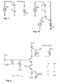
- Fig. 1 shows a driver for controlling an organic light emitting diode DO.
- the circuit consists of a voltage source Vdc, a capacitor C1, a switch S and the organic light emitting diode DO.
- the diode DO has an anode and a cathode. The cathode is connected to ground potential.
- the anode of the diode DO is connectable to one electrode of the capacitor C1 via the switch S.
- the opposite electrode of the capacitor is connected to ground potential.
- the voltage source Vdc may also be connected via the switch S to the capacitor.
- the voltage source is referenced to ground potential. Ground potential is only chosen for convenience. Any predetermined reference potential may be chosen instead.
- the switch S either connects the voltage Source Vdc with the capacitor or the diode DO with the capacitor. The voltage source and the diode are never simultaneously connected to the capacitor C1.
- the circuit of Fig. 1 is operated by alternately connecting the voltage source Vdc and the diode DO to the capacitor.
- the voltage source charges the capacitor C1 to its output voltage as long as it is connected to the capacitor.
- the capacitor is discharged via the diode DO.
- a current flows through the diode, which depends on the potential difference between the capacitor voltage and ground potential.
- the luminance of the diode may be controlled by applying a desired charge to the capacitor C1, resulting in a corresponding voltage, which in turn produces a current through the diode determining the luminance.
- the current I DO is proportional to the charge voltage, or, put more correctly: The current is proportional to the voltage difference between the charged and the discharged state of the capacitor. Good picture uniformity can be achieved, since frequency control and stability, capacitor matching and also a good voltage precision can be achieved within narrow tolerances.
- An active matrix OLED display is a type of display, which uses transistors for switching individual light emitting elements of a display.
- the active matrix display may contain, besides the light emitting elements, a matrix of thin-film transistors (TFTs). These devices store the electrical state of an individual pixel on the display while all the other pixels are being updated. This method provides a much brighter, sharper display than a passive matrix of the same size.
- TFTs thin-film transistors
- Thin film transistors may be used for constructing an active matrix.
- a thin film transistor is just one component in an active matrix and some designs have used other active components such as diodes.
- a passive matrix display uses a simple conductive grid to deliver current to the light emitting element in the target area, whereas an active matrix display uses a grid of transistors and capacitors, which may be integrated together with the thin film transistors, with the ability to hold a charge for a limited period of time. Because of the switching action of transistors, only capacitor associated with the desired pixel receives a charge, and the capacitor holds the charge until the next refresh cycle, improving image quality over a passive matrix.
- Integrated MOS capacitors typically have a capacitance per area in a range of 5 fF per micron square.
- 5x5 ⁇ m pixel 20 fF for the charge capacitor can be assumed, when an area of 2x2 ⁇ m is used for the capacitor.
- a ramp-like control voltage may be used. That is, the output voltage of the voltage source V dc may be controlled to continually increase, while the voltage source is connected to the switch. The peak current occurs, when the voltage difference between the voltage source and the capacitor is greatest. This is the case, when the voltage source is connected to the capacitor C1.
- the ramp-like output voltage reduces the peak current in comparison with an output voltage, which is applied in a step-like manner.
- Vth mismatches i.e. variations between threshold voltages Vth of individual MOS transistors.
- a first rough analysis has shown that on mono crystalline silicon, and assuming FS (Full Scale) voltage amplitudes of 2V, the Vth mismatch is essentially negligible. Anyhow, some mismatch compensation is included in some of the following circuits.
- Fig. 2 shows an exemplary circuit using n-channel FETs (field effect transistors).
- corresponding elements are designated by the same reference signs.
- the circuit shown in Fig. 2 represents a single element in an active matrix display. Each light emitting element in the display may be addressed using a column and row line. A column line is connected to each light emitting element in a column of the matrix; a row line is connected to each light emitting element in a row of the matrix. The column line and row line are designated by reference signs Col und Row in Fig. 2 .
- Fig. 2 comprises a light emitting diode DO, which has an anode connected to a constant reference voltage Vdio.
- the circuit of Fig. 2 differs from the circuit of Fig. 1 , in which the current to the anode of the diode DO was controlled.
- the cathode of the light emitting diode DO is connected via field effect transistor N2 and N4 to a capacitor C1.
- Source s of transistor N2 is connected to the drain of transistor N4.
- the drain current of transistor N2 corresponds to the current flowing through the light emitting diode DO.
- the drain current of N2 roughly corresponds to the source current s of transistor N4.
- the luminosity of diode DO is controlled by charging and discharging capacitor C1 connected to the source of transistor N4.
- the amount of current flowing through diode DO depends on the voltage difference between the voltage applied to the gate of transistor N2 and the voltage drop over the drain d and source s of transistor N2.
- the current is controlled by the gate voltage g of the transistor, which in turn is controlled by the column and row signals.
- a transistor N1 is connected to both to the column and row line as well as the gate of transistor N2.
- the gate of transistor N1 is connected to the row line. If the row line carries a high voltage signal, then the drain-source channel of the transistor N1 is made conductive.
- the voltage signal on the column line connected to the drain of transistor N1 is transferred to the source of transistor N1 as well as the gate of transistor N2. In this instance, the transistor N2 is operated in the saturation region.
- the node g is set to the programming voltage. This is done by applying the programming voltage to the column line Col and applying a high pulse to the row line Row. The programming is usually done synchronously, line by line, with the incoming video signal.
- the voltage at the source s of transistor N2 is equal to the voltage on C0 minus the gate source voltage drop.
- the capacitor C1 is repeatedly charged to roughly the voltage on C0 by making N4 conductive for a time.
- the source follower transistor N2 and the voltage on C0 determine when the charging is completed.
- the current flowing through transistors N2 and N4 is also the current through the light emitting diode DO.
- the capacitor After having charged the capacitor C1, the capacitor is disconnected from the source of transistor N2 using a low voltage on the gate of transistor N4. During this time, C1 is discharged. This is achieved by connecting the source of transistor N4 to ground. To this end, a transistor N3 operated in parallel with the capacitor C1 receives a high voltage Vres at its gate. The process of charging capacitor C1 resumes by applying a low voltage Vres to the gate of transistor N3 and applying a high voltage Von to the gate of transistor N4.
- a table shows exemplary voltage signals for Von and Vcap1. Each entry in the table represents the amplitude of voltage signals Von and Vcap1 versus time.
- Vcap is a voltage applied to the electrode of capacitor C0 opposite to the electrode connected to the gate of transistor N2.
- Controlling Vcap1 can help also to shift the possible voltages on the column Col to a suitable range during the programming period, and afterwards to a different level for best charge pump operation.
- the voltage of capacitor C0 can be adjusted using the voltage Vcap1.
- the voltage Von represents the voltage applied to the gate of transistor N4.
- a high voltage Von increases the current flowing to capacitor C1.
- a period of the voltage Von follows a square wave function, whereas the voltage Vcap1 has a saw tooth shape.
- the saw tooth voltage gradually increases the voltage on the gate of transistor N2 as well as the current flowing to the capacitor C1, while the gate of transistor N4 receives a high signal.
- peak currents flowing to the capacitor and light emitting diode can be reduced. Consequently, the current and luminance of light emitting diode DO is essentially constant as the capacitor C1 is being loaded.
- the voltage Von has a saw tooth form, whereas the voltage Vcap1 is connected to ground potential.
- transistor N4 is used for reducing the peak current flowing to the capacitor C1.
- a high peak current would flow, if a high voltage were immediately applied to the gate of transistor N4.
- the voltage difference between the drain and source of transistor is greatest, leading to a peak current.
- the capacitor C1 is gradually charged, the voltage difference between the source and drain of the transistor is gradually reduced.
- the peak current is reduced and generally the current into capacitor C1 is controlled by gradually increasing the gate voltage Von of transistor N4.
- transistor N4 is operated as a controllable resistor, whereby the voltage drop across the drain and source of transistor N2 may be controlled in a suitable manner.
- the circuit of Fig. 2 may additionally comprise a transistor N5 or a diode D1.
- transistor N5 acts as a diode, since the drain of transistor N5 is connected to the gate of transistor N5.
- the anode of diode N1 and the transistor N5 acting as a diode is connected to the cathode of the light emitting diode DO.
- the cathode of diode D1 is driven with a supply voltage Vdd.
- the additional diode may serve different purposes, in particular:
- Voltages Vcap 2, and also Vcap1 can be connected to either supply voltage Vdd or ground voltage GND. Connecting to ground voltage GND is preferable in order to avoid detrimental effects caused by additional AC current components on the supply rails. However, for capacitor implementation reasons, the supply voltage Vdd can also be used.
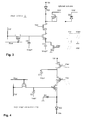
- Figure 3 shows an example not falling under the scope of the claims of the present application.
- the example of Fig. 3 largely corresponds to the embodiment of Fig. 2 .
- Identical components are designated with the same reference numerals in Fig. 2 and 3 .
- the only difference between Fig. 2 and Fig. 3 is the placement of transistor N4 relative to the light emitting diode DO, transistor N2 and the capacitor C1.
- the transistor N4 is arranged between the diode DO and the transistor N2.
- the position of transistors N2 and N4 have been exchanged.
- the overall function of the circuit is the same. Either of the circuits presented in figure 2 or figure 3 can be preferable for layout reasons.
- the optional addition of transistor N5 and D5 is identical to Fig. 2 .
- the proposed operation of transistor N4 and capacitor Vcap1 using the signals represented in the accompanied table of Fig. 3 is identical with Fig. 2 .
- Figure 4 shows a similar topology as Fig. 2 .
- N-channel transistors N1, N2, N3 and N4 of Fig. 2 correspond to p-channel transistors P1, P2, P3 and P4 of Fig. 4 , respectively.
- the signals input to the gates of each transistor P1 to P4 are inverted. This is done, because a p-channel transistor must be operated with a negative gate voltage with respect to its source electrode, whereas an n-channel transistor requires a positive gate voltage.
- the anode instead of the cathode of the light emitting diode DO is connected to transistors P2, P4 and capacitor C1 in the series connection.
- Capacitors C0 and C1 have their reference terminals connected to Vdd or GND. Swapping the order of P2 and P4 is also an option here, similar as described under Fig. 3 .
- p-channel-MOS devices may be preferred because many common OLED displays use a common top electrode, which is the cathode (Vdio).
- Vdio the cathode
- P4 and P2 may be swapped in order.
- Fig. 4 additionally shows exemplary voltage signals Vres and Von over time, which drive the transistor P3 and P4, respectively.
- Transistor P3 is driven by a square wave signal. The effect of this signal is to connect capacitor C1 with the supply voltage Vdd in order to discharge capacitor C1.
- the source of transistor P3 may also be connected to ground potential GND.
- the square wave pulses periodically discharge capacitor C1.
- the capacitor C1 is charged by applying a saw tooth shaped voltage Von applied to the gate of capacitor P4.
- the saw tooth shape brings about a relatively constant current, which drives the light emitting diode DO and charges the capacitor C1, as explained further above.
- Figure 5 shows a representation of the circuit for controlling a light emitting element DO according to another example not falling under the scope of the claims of the present application.
- the circuit of Fig. 5 uses n-channel transistors for driving the diode.
- the arrangement of the circuit of Fig. 5 largely corresponds to the circuit according to Fig. 2 .
- the transistor N4 has been omitted in Fig. 5 .
- the arrangement of transistors and capacitors is identical in Fig. 2 and Fig. 5 .
- the operation of the circuit of Fig. 5 differs from the operation of the circuit of Fig. 2 , since the switching transistor N4 is missing in Fig. 5.
- Fig. 5 shows a representation of the circuit for controlling a light emitting element DO according to another example not falling under the scope of the claims of the present application.
- the circuit of Fig. 5 uses n-channel transistors for driving the diode.
- the arrangement of the circuit of Fig. 5 largely corresponds to the circuit according to Fig. 2
- Vcap voltage signals
- Vres and Row over time which are applied to the capacitor C0, the gate of transistor Vres and the row line, respectively.
- the amplitude of each voltage is shown to change with time.
- the voltage on the column line is applied to the gate of transistor N2 by a rectangular pulse row voltage signal.
- the voltage Vcap is reduced in a step-like fashion. Consequently, transistor N2 is operated in the cut-off region.
- the capacitor C1 is connected to ground by applying a square wave voltage signal Vres to the gate of transistor N3.
- n-channel transistor N3 is opened, i.e. does not conduct, and the gate voltage of transistor N2 is gradually increased using a ramp voltage signal Vcap at the capacitor C0. Consequently, a substantially constant current flow through the light emitting diode DO is established for a certain period in time, i.e. throughout the drive period.
- FIG. 6 shows another example not falling under the scope of the claims of the present application.
- the circuit of Fig. 6 is composed of n-channel transistors N1 to N5, capacitors C0 and C1 as well as light emitting diode DO.
- the arrangement of capacitor C0 and transistor N1 in Fig. 6 corresponds to the arrangement of Fig. 5 .
- the capacitor C1 is directly connected to the anode of the light emitting diode DO.
- Transistor N2 is connected with its source to capacitor C1 in a series connection.
- the base of transistor N2 is driven by the column line when transistor N1 is operated in the saturation region by applying a high voltage to the base transistor N1.
- Transistor N3 is connected to capacitor C1 in order to discharge the capacitor.
- the drain of transistor N3 is connected to ground potential.
- transistors N5 and N4 have been added to the circuit of Fig. 5 .
- Transistor N5 is operated as diode by connecting the source and base of transistor N5 to ground potential.
- the drain of transistor N5 is also connected to the anode of light emitting diode DO. Therefore, the transistor basically prevents that the potential of the anode of the light emitting diode DO drops far below ground potential.
- transistor N3 connects the capacitor with ground potential for resetting the potential of the anode of the light emitting diode is pulled up by the charge current through the diode, which is formed by transistor N5 in this figure.
- This reset creates a dependency on the threshold voltage Vth of transistor N5, since the drain voltage of N5, which corresponds to the anode voltage of DO, should be approximately equal to ground potential minus the threshold voltage Vth.
- the cathode of the light emitting diode DO is connected to the diode voltage Vdio.
- the cathode voltage Vdio should be chosen in such a way that no current flows through the diode DO once the capacitor C1 has been discharged.
- This circuit has the advantage that it presents a true n-channel based solution.
- the gates of n-MOS are on high voltages, not only the drain nodes.
- the light emitting diode DO is in the source path of the transistor N2, so its electrical characteristics, e.g. the U/l-characteristic or the forward voltage of the light emitting diode DO, have an influence.
- the capacitor C1 has no node on a supply level Vdd.
- the cathode voltage Vdio is chosen to be a negative voltage in relation to ground voltage.
- the light emitting diode DO may just not conduct, when the anode is on substrate ground level.
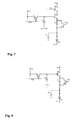
- Figure 7 shows a depiction of another example not falling under the scope of the claims of the present application.
- the circuit of Fig. 7 largely corresponds to the circuit of Fig. 6 .
- transistor N3 connects the source of transistor N2 with the anode of the light emitting diode DO. Therefore, the capacitor is discharged by short circuiting both sides of the capacitor C1.
- a Diode D1 is connected to the anode of the light emitting diode DO.
- the diode D1 performs the same function as the transistor N5 in Fig. 6 , which is operated as diode.
- Diode D1 may be a part of transistor N3 and is then formed by connecting an active n + -region to the p-doted substrate of the transistor. Capacitor is charged using transistors N2 and N4. The gate voltage of transistor N4 is ramp-shaped in order to supply a substantially constant current during driving. The capacitor, which is being charged, drives the current through the light emitting diode DO.
- Fig. 8 illustrates another example not falling under the scope of the claims of the present application.
- the circuit of Fig. 8 corresponds essentially to the circuit of Fig. 7 .
- the circuit of Fig. 8 does not comprise switching transistor N4. Instead the drain of transistor N2 is connected to the supply voltage Vdd. Otherwise the two embodiments seven and eight are identical.
- care must be taken during reset of capacitor C1 in order to avoid any current flow through transistor N2. Therefore, the voltage Vcap applied to the capacitor C0 must be chosen appropriately. Vcap must be pulled down in order to reduce the potential at the gate of transistor N2. Consequently, the transistor is operated in the cut-off region, while the capacitor C1 is being discharged. In this circuit one charge pulse during programming may be required.
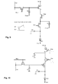
- Figure 9 shows a circuit for controlling a light emitting diode according to the second embodiment of the present invention: A pixel circuit based on n-MOS devices and with an OLED of common cathode type. Transistors N2 and N4 may be swapped in order, similar to embodiments described further above. The arrangement of transistors N1, N2, capacitor C0 and column and row lines Col and Row are identical with the arrangement of the example of Fig. 8 .
- the anode of the light emitting diode DO is connected to a cathode of a diode D1 and a source of transistor N3.
- a charging capacitor is connected to the drain of transistor N3, which is driven by a gate voltage Von.
- the capacitor C1 is not directly connected to the anode of the light emitting diode DO.
- Capacitor C1 is discharged by gradually increasing the gate voltage Von of transistor N3; the voltage signal Von versus time is graphically represented in Fig. 9 .
- Both the capacitor C1 and the drain of transistor N3 are connected to the source of transistor N4, which is driven by a gate voltage Vres. While the capacitor C1 is being discharged by ramping the gate voltage Von, the gate voltage Vres of transistor N4 is in a low state; i.e. transistor N4 is operated in the cut-off region. Therefore, the source current of transistor N4 is zero and the whole discharge current of capacitor C1 flows through the light emitting diode DO; the discharge current does not flow through diode D1, since diode D1 is connected with its cathode to transistor N3.
- the charging of capacitor C1 is accomplished by operating transistor N3 in the cut-off region, such that a current from transistor N4 flows completely to circuit node g of capacitor C1.
- a rectangular pulse voltage signal Vres is applied to the gate of transistor N4, while the gate voltage Von of transistor N3 is low.
- the magnitude of the charging current depends both on the gate voltage of transistor N2 and the supply voltage Vdd supplied to the drain of transistor N2.
- the gate voltage is not ramped, since it is not necessary to provide a constant current for charging the capacitor C1.
- Transistor Vres is simply operated as a switch in order to charge the capacitor C1.
- the gate voltage of transistor N2 is essentially equal to the voltage on column line Col, when transistor is operated in the saturation region using an appropriate row line voltage.
- Capacitor C0 is connected with one electrode to the gate of transistor N2 and with the opposite electrode to voltage Vcap0. Capacitor C0 stores the voltage from the column line Col. Vcap0 may be chosen to be equal to the supply voltage Vdd or ground potential GND.
- One electrode of capacitor C1 is connected to the source of transistor N4 as well as the drain of transistor N3; the other electrode of capacitor C1 is connected to a voltage Vcap1, which may be chosen to be equal to the supply voltage Vdd or ground potential.
- Vcap0 and Vcap1 When Vcap0 and Vcap1 are connected to supply voltage Vdd the capacitors C0 and C1 may be advantageously implemented as p-MOS capacitors.
- Diode D1 may be formed by the intrinsic diode of transistor N3. This embodiment advantageously has no floating capacitor.
- Figure 10 shows the circuit according to another example not falling under the scope of the claims of the present application.
- the circuit of Fig. 10 corresponds to the circuit of Fig. 4 save for two exceptions. Firstly, in Fig. 4 capacitor C0 is connected to potential Vcap1, whereas capacitor C0 in Fig. 10 is connected to ground. Secondly, capacitor C1 in Fig. 4 is connected to the voltage Vcap2, whereas the corresponding capacitor C1 in Fig. 10 is also connected to ground.
- the diode current of the light emitting diode DO of Fig. 10 is controlled by charging and discharging capacitor C1.
- Figure 11 shows an exemplary circuit according to the invention used for simulating voltages and currents of the charge pump.
- the simulation circuit essentially corresponds to the circuit of figure 10 .
- the programming transistor P1 and the storage capacitor C0 were replaced by a DC voltage source V2, since the main interest of the simulation was the analysis of the charge pump function.
- the OLED DO has been replaced by a series connection of 5 silicon diodes D4, D6, D8, D9 and D10 for taking the higher forward voltage of OLEDs cf. silicon diodes into account.
- Diode D1 avoids over-voltage breakdown at the drain of the drive transistor M1, which corresponds to transistor P2 in figure 10 , when no current is flowing.
- capacitor C0 corresponding to capacitor C1 in figure 10
- the cathode of the light emitting diode DO is connected to the voltage Vdio, which may be equal to -2V.
- Vdio of figure 10 is represented by voltage source V1 in figure 11 .
- the supply voltage Vdd represented by voltage source V0 in figure 11
- the reset voltage Vres is a square shape pulsed signal, which is applied to the base of transistor M3, which corresponds to transistor P3 in figure 10 .
- the capacitance of the charging capacitor C1 may be chosen to be equal to 10 fF.
- the pump capacitor C0 (C1 in figure 10 ) is charged to approximately 2V - Vth, corresponding to the maximum brightness case.
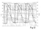
- Figure 12 shows simulated results for the circuit of figure 11 .
- the waveforms in Fig. 12 show in the upper part voltages, including the control voltages applied to the circuit.
- the bottom line represents the current into the OLED. It can be seen that in the centre part of each 10 us period, the current is essentially constant at 3 nA. Average current is around 1 nA. This can be seen best in the second and third period, since some voltage initialization is visible the first period.
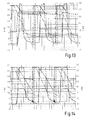
- Figure 13 shows simulated waveforms with the pump capacitor C1 charged to 1.5V - Vth. A comparison with the waveforms in figure 11 clearly shows a lower average current. The reason is mainly a shortened time of current flow.
- Figure 14 shows simulated waveforms for a circuit in which the transistors corresponding to P2 and P4 in figure 11 are swapped. No major difference is visible.
- FIG. 15 shows a diagrammatic representation of a further development of a circuit according to the invention.
- capacitor C1 is coupled to the light emitting means DO during charge and discharge, however with respective opposite electrodes.
- the charge current causes the light emitting means coupled to one electrode of the capacitor to emit light.
- the other electrode is of course coupled to a charge voltage source, preferably via a controllable voltage regulator that allows for adjusting a desired voltage waveform. If the charge voltage has an appropriate waveform, e.g. sawtooth shape as elucidated further above, the charge current and thus the current through the diode is essentially constant. Otherwise a current control means may be provided for controlling the current during charging.
- the voltage source used for charging is disconnected from the capacitor.
- the electrode of the capacitor that has the higher potential is now coupled to the light emitting means DO instead being coupled to the voltage source.
- the other electrode of the capacitor is coupled to a reference potential lower than the voltage across the capacitor.
- the reference potential may be ground, or a voltage source essentially corresponding to the forward voltage drop of the light emitting means, allowing for a complete discharge of the capacitor.
- the discharge current now flows through the light emitting means, causing it to emit light also during this phase of operation. If the discharge current is controlled to be essentially linear the total time during which light of a desired intensity is emitted can approximately be doubled. Switches S1 and S2 need of course be controlled such that they alternately connect the capacitor to the light emitting means, and cross connection of the charge voltage and the reference potential are to be avoided, although not causing a possible dangerous DC short circuit.
- the current flow duty cycle can be increased.
- a trade-off between capacitor size, clock rate, and the amplitude of the clock signals will influence the dynamic dissipation.
- the over voltage diode D1 is in fact useful. This simulation proves that no 5V transistors are required. In terms of active devices, a standard logic process like 0.18u 1.8V/3.3V could for example be used, making manufacturing of this circuit easy and inexpensive. It is also conceivable to use only 3.3V devices, further reducing complexity of the production process.
Landscapes
- Engineering & Computer Science (AREA)
- Physics & Mathematics (AREA)
- Computer Hardware Design (AREA)
- General Physics & Mathematics (AREA)
- Theoretical Computer Science (AREA)
- Control Of Indicators Other Than Cathode Ray Tubes (AREA)
- Electroluminescent Light Sources (AREA)
- Control Of El Displays (AREA)
Description
- The invention relates to a driver and method for controlling a light emitting element, in particular an organic light emitting diode OLED. These OLEDS may be used as pixels in micro displays. An organic light-emitting diode (OLED) is a special type of light-emitting diode (LED), in which the emissive layer comprises a thin-film of certain organic compounds. The emissive electroluminescent layer can include a polymeric substance that allows the deposition of suitable organic compounds, for example, in rows and columns on a carrier by using a simple "printing" method to create a matrix of pixels which can emit different colour light.
- OLED displays can be used in television screens, computer displays, portable system screens, and in advertising and information and indication applications etc. OLEDs can also be used in light sources for general illumination. OLEDs lend themselves for the implementation of large area light-emitting elements. One of the great benefits of an OLED display over the traditional LCD displays is that OLEDs do not require a backlight to function. This means that they draw far less power and, when powered from a battery, can operate longer on the same charge.
- Micro displays can be based on a substrate of mono-crystalline silicon, on which the electronic circuits required for driving are disposed. Layers of OLED material are deposited on one surface of the substrate.
- Micro displays face several technical problems, amongst which are:
- limited space for circuit elements in the available cell area;
- high voltage operation (3..5V);
- very small OLED diode current, e.g. < 1 nA, needing e.g. sub threshold operation of transistors and incurring sensitivity to leakage currents;
- I/U characteristic of OLED influencing the current and thus the picture homogeneity; and
- difficulties in the required dynamic for programming of pixels due to small currents.
-
JP 2002-289374A - It is an object of the present invention to provide an improved driver for controlling a light emitting element (DO), which overcomes the drawbacks of the state of the art.
- The object is solved by a driver for controlling a light emitting element, in particular an organic light emitting diode according to the appended claims. The driver comprises a capacitor connectable with the light emitting element, charging means for charging the capacitor and a switching means. The switching means is adapted to alternately disconnect the capacitor from the light emitting element and connect the capacitor to the light emitting element. The capacitor is alternately charged and discharged. A charging current or a discharge current from the capacitor drives the current of the light emitting element. Said charging means comprises at least one charging transistor for charging the capacitor.
- The circuits according to the invention described in the following present a new circuit for generating the OLED diode current. The current is set by charging and discharging a capacitor at a given clock frequency.
- Preferred embodiments and comparative examples are described hereinafter with reference to the drawings, in which
-
Fig. 1 depicts the basic principle of the present invention; -
Fig. 2 shows a first embodiment of the present invention; -
Fig. 3 shows an example not falling under the scope of the claims of the present application; -
Fig. 4 shows another example not falling under the scope of the claims of the present application; -
Fig. 5 shows another example not falling under the scope of the claims of the present application; -
Fig. 6 shows another example not falling under the scope of the claims of the present application; -
Fig. 7 shows another example not falling under the scope of the claims of the present application; -
Fig. 8 shows another example not falling under the scope of the claims of the present application; -
Fig. 9 shows a second embodiment of the present invention; -
Fig. 10 shows another example not falling under the scope of the claims of the present application; -
Fig. 11 shows a circuit used for simulating voltages and currents; -
Fig. 12 shows waveforms of a first simulation of an embodiment of the invention; -
Fig. 13 shows waveforms of a second simulation of an embodiment of the invention; -
Fig. 14 shows waveforms of a third simulation of an embodiment of the invention; and -
Fig. 15 shows a diagrammatic representation of a further development of a circuit according to the invention. - The basic principle of the present invention is illustrated in
Fig. 1. Fig. 1 shows a driver for controlling an organic light emitting diode DO. The circuit consists of a voltage source Vdc, a capacitor C1, a switch S and the organic light emitting diode DO. The diode DO has an anode and a cathode. The cathode is connected to ground potential. The anode of the diode DO is connectable to one electrode of the capacitor C1 via the switch S. The opposite electrode of the capacitor is connected to ground potential. Furthermore, the voltage source Vdc may also be connected via the switch S to the capacitor. The voltage source is referenced to ground potential. Ground potential is only chosen for convenience. Any predetermined reference potential may be chosen instead. The switch S either connects the voltage Source Vdc with the capacitor or the diode DO with the capacitor. The voltage source and the diode are never simultaneously connected to the capacitor C1. - The circuit of
Fig. 1 is operated by alternately connecting the voltage source Vdc and the diode DO to the capacitor. The voltage source charges the capacitor C1 to its output voltage as long as it is connected to the capacitor. When the capacitor is connected to the diode DO, the capacitor is discharged via the diode DO. A current flows through the diode, which depends on the potential difference between the capacitor voltage and ground potential. The luminance of the diode may be controlled by applying a desired charge to the capacitor C1, resulting in a corresponding voltage, which in turn produces a current through the diode determining the luminance. - The basic principle is shown in
Fig 1 . The diode current (idealized) is given by:
wherein fs is the switching frequency of the switch S, C1 is the capacity of the capacitor C1 and Vdc is the voltage of the voltage source Vdc. The current IDO is proportional to the charge voltage, or, put more correctly: The current is proportional to the voltage difference between the charged and the discharged state of the capacitor. Good picture uniformity can be achieved, since frequency control and stability, capacitor matching and also a good voltage precision can be achieved within narrow tolerances. - The above-mentioned principle may be applied to circuits for active matrix OLED displays, which allow better display performance and life time of the OLEDs due to the inherent smaller currents in operation when compared to passive matrix OLED displays. An active matrix OLED display (AMOLED) is a type of display, which uses transistors for switching individual light emitting elements of a display.
- The active matrix display may contain, besides the light emitting elements, a matrix of thin-film transistors (TFTs). These devices store the electrical state of an individual pixel on the display while all the other pixels are being updated. This method provides a much brighter, sharper display than a passive matrix of the same size.
- Thin film transistors may be used for constructing an active matrix. However, a thin film transistor is just one component in an active matrix and some designs have used other active components such as diodes. A passive matrix display uses a simple conductive grid to deliver current to the light emitting element in the target area, whereas an active matrix display uses a grid of transistors and capacitors, which may be integrated together with the thin film transistors, with the ability to hold a charge for a limited period of time. Because of the switching action of transistors, only capacitor associated with the desired pixel receives a charge, and the capacitor holds the charge until the next refresh cycle, improving image quality over a passive matrix.
- Integrated MOS capacitors typically have a capacitance per area in a range of 5 fF per micron square. For an exemplary 5x5 µm pixel 20 fF for the charge capacitor can be assumed, when an area of 2x2 µm is used for the capacitor. Operating the switch S at 32 kHz and assuming a voltage for Full Scale (FS) of 2V, the average diode current will have a FS value of

- For avoiding high peak currents when switches are closing a ramp-like control voltage may be used. That is, the output voltage of the voltage source Vdc may be controlled to continually increase, while the voltage source is connected to the switch. The peak current occurs, when the voltage difference between the voltage source and the capacitor is greatest. This is the case, when the voltage source is connected to the capacitor C1. The ramp-like output voltage reduces the peak current in comparison with an output voltage, which is applied in a step-like manner.
- A detailed analysis shows the impact of Vth mismatches, i.e. variations between threshold voltages Vth of individual MOS transistors. A first rough analysis has shown that on mono crystalline silicon, and assuming FS (Full Scale) voltage amplitudes of 2V, the Vth mismatch is essentially negligible. Anyhow, some mismatch compensation is included in some of the following circuits.
-
Fig. 2 shows an exemplary circuit using n-channel FETs (field effect transistors). InFig. 2 , corresponding elements are designated by the same reference signs. - The circuit shown in
Fig. 2 represents a single element in an active matrix display. Each light emitting element in the display may be addressed using a column and row line. A column line is connected to each light emitting element in a column of the matrix; a row line is connected to each light emitting element in a row of the matrix. The column line and row line are designated by reference signs Col und Row inFig. 2 . -
Fig. 2 comprises a light emitting diode DO, which has an anode connected to a constant reference voltage Vdio. In this respect, the circuit ofFig. 2 differs from the circuit ofFig. 1 , in which the current to the anode of the diode DO was controlled. The cathode of the light emitting diode DO is connected via field effect transistor N2 and N4 to a capacitor C1. Source s of transistor N2 is connected to the drain of transistor N4. The drain current of transistor N2 corresponds to the current flowing through the light emitting diode DO. Furthermore, the drain current of N2 roughly corresponds to the source current s of transistor N4. The luminosity of diode DO is controlled by charging and discharging capacitor C1 connected to the source of transistor N4. - The amount of current flowing through diode DO depends on the voltage difference between the voltage applied to the gate of transistor N2 and the voltage drop over the drain d and source s of transistor N2. The current is controlled by the gate voltage g of the transistor, which in turn is controlled by the column and row signals. A transistor N1 is connected to both to the column and row line as well as the gate of transistor N2. The gate of transistor N1 is connected to the row line. If the row line carries a high voltage signal, then the drain-source channel of the transistor N1 is made conductive. The voltage signal on the column line connected to the drain of transistor N1 is transferred to the source of transistor N1 as well as the gate of transistor N2. In this instance, the transistor N2 is operated in the saturation region. During the programming phase, the node g is set to the programming voltage. This is done by applying the programming voltage to the column line Col and applying a high pulse to the row line Row. The programming is usually done synchronously, line by line, with the incoming video signal.
- The voltage at the source s of transistor N2 is equal to the voltage on C0 minus the gate source voltage drop. The capacitor C1 is repeatedly charged to roughly the voltage on C0 by making N4 conductive for a time. The source follower transistor N2 and the voltage on C0 determine when the charging is completed. The current flowing through transistors N2 and N4 is also the current through the light emitting diode DO.
- After having charged the capacitor C1, the capacitor is disconnected from the source of transistor N2 using a low voltage on the gate of transistor N4. During this time, C1 is discharged. This is achieved by connecting the source of transistor N4 to ground. To this end, a transistor N3 operated in parallel with the capacitor C1 receives a high voltage Vres at its gate. The process of charging capacitor C1 resumes by applying a low voltage Vres to the gate of transistor N3 and applying a high voltage Von to the gate of transistor N4.
- In
Fig. 2 , a table shows exemplary voltage signals for Von and Vcap1. Each entry in the table represents the amplitude of voltage signals Von and Vcap1 versus time. Vcap is a voltage applied to the electrode of capacitor C0 opposite to the electrode connected to the gate of transistor N2. - Controlling Vcap1 can help also to shift the possible voltages on the column Col to a suitable range during the programming period, and afterwards to a different level for best charge pump operation. In particular, while the gate of transistor N1 receives a low signal, the voltage of capacitor C0 can be adjusted using the voltage Vcap1. The voltage Von represents the voltage applied to the gate of transistor N4. A high voltage Von increases the current flowing to capacitor C1. In the first line of the table, a period of the voltage Von follows a square wave function, whereas the voltage Vcap1 has a saw tooth shape. The saw tooth voltage gradually increases the voltage on the gate of transistor N2 as well as the current flowing to the capacitor C1, while the gate of transistor N4 receives a high signal. Thereby, peak currents flowing to the capacitor and light emitting diode can be reduced. Consequently, the current and luminance of light emitting diode DO is essentially constant as the capacitor C1 is being loaded.
- In the second row of the table of
Fig. 2 , the voltage Von has a saw tooth form, whereas the voltage Vcap1 is connected to ground potential. In this case, transistor N4 is used for reducing the peak current flowing to the capacitor C1. A high peak current would flow, if a high voltage were immediately applied to the gate of transistor N4. In this instance, the voltage difference between the drain and source of transistor is greatest, leading to a peak current. Since the capacitor C1 is gradually charged, the voltage difference between the source and drain of the transistor is gradually reduced. The peak current is reduced and generally the current into capacitor C1 is controlled by gradually increasing the gate voltage Von of transistor N4. In this case transistor N4 is operated as a controllable resistor, whereby the voltage drop across the drain and source of transistor N2 may be controlled in a suitable manner. - The circuit of
Fig. 2 may additionally comprise a transistor N5 or a diode D1. In the figure transistor N5 acts as a diode, since the drain of transistor N5 is connected to the gate of transistor N5. The anode of diode N1 and the transistor N5 acting as a diode is connected to the cathode of the light emitting diode DO. The cathode of diode D1 is driven with a supply voltage Vdd. The additional diode may serve different purposes, in particular: - In the case of a high voltage operation and a low voltage CMOS process: If the voltage Vdio exceeds the maximum permitted IC supply voltage Vdd, the diode, e.g. N5, limits the voltage present at the drain electrode of transistor N2.
- In order to provide a certain degree of testability, the diode N5 or D1 can be used to form a current path during steps of manufacturing, e.g. in case the OLED device is not yet deposited on top of the transistor array or matrix. Manufacturing tests of raw wafers with reasonable test coverage are thus possible. In this case supply voltage Vdd could for example be applied to separate column or row lines.
- In order to provide a certain degree of Vth compensation it is, for example, possible to provide a time period during which the OLED is intentionally shorten by the diode. This can be achieved by pulling down Vdio. Then, the voltage Vcap1 and consequently the voltage of the gate of transistor N2 are ramped up slightly, so that transistor N2 starts to conduct. In this instance, the field effect transistor N2 is operated on the verge between the saturation region and the ohmic region. Capacitor C1 and equally the source of transistor N2 reaches a voltage, which is lower by Vth of N2 than the gate voltage of transistor N2. Vth is the threshold voltage of transistor N, which may vary due to production tolerances. The resulting current is independent of the threshold voltage Vth of transistor N2 and its tolerance.
- Voltages Vcap 2, and also Vcap1 can be connected to either supply voltage Vdd or ground voltage GND. Connecting to ground voltage GND is preferable in order to avoid detrimental effects caused by additional AC current components on the supply rails. However, for capacitor implementation reasons, the supply voltage Vdd can also be used.
-
Figure 3 shows an example not falling under the scope of the claims of the present application. The example ofFig. 3 largely corresponds to the embodiment ofFig. 2 . Identical components are designated with the same reference numerals inFig. 2 and3 . The only difference betweenFig. 2 andFig. 3 is the placement of transistor N4 relative to the light emitting diode DO, transistor N2 and the capacitor C1. In the third embodiment ofFig. 3 , the transistor N4 is arranged between the diode DO and the transistor N2. The position of transistors N2 and N4 have been exchanged. The overall function of the circuit is the same. Either of the circuits presented infigure 2 orfigure 3 can be preferable for layout reasons. The optional addition of transistor N5 and D5 is identical toFig. 2 . Furthermore, the proposed operation of transistor N4 and capacitor Vcap1 using the signals represented in the accompanied table ofFig. 3 is identical withFig. 2 . -
Figure 4 shows a similar topology asFig. 2 . N-channel transistors N1, N2, N3 and N4 ofFig. 2 correspond to p-channel transistors P1, P2, P3 and P4 ofFig. 4 , respectively. Unlike the embodiment ofFig. 2 , the signals input to the gates of each transistor P1 to P4 are inverted. This is done, because a p-channel transistor must be operated with a negative gate voltage with respect to its source electrode, whereas an n-channel transistor requires a positive gate voltage. Furthermore, the anode instead of the cathode of the light emitting diode DO is connected to transistors P2, P4 and capacitor C1 in the series connection. The direction of the source-drain current of the p-channel transistors is reversed in relation to the current direction of the corresponding n-channel transistors. Therefore, the anode of light emitting diode instead of the cathode is chosen in the embodiment ofFig. 4 . Capacitors C0 and C1 have their reference terminals connected to Vdd or GND. Swapping the order of P2 and P4 is also an option here, similar as described underFig. 3 . - Using p-channel-MOS devices may be preferred because many common OLED displays use a common top electrode, which is the cathode (Vdio). As for the n-channel circuit of
Figs. 2 and3 , P4 and P2 may be swapped in order.Fig. 4 additionally shows exemplary voltage signals Vres and Von over time, which drive the transistor P3 and P4, respectively. Transistor P3 is driven by a square wave signal. The effect of this signal is to connect capacitor C1 with the supply voltage Vdd in order to discharge capacitor C1. Alternatively, the source of transistor P3 may also be connected to ground potential GND. The square wave pulses periodically discharge capacitor C1. Intermittently, the capacitor C1 is charged by applying a saw tooth shaped voltage Von applied to the gate of capacitor P4. The saw tooth shape brings about a relatively constant current, which drives the light emitting diode DO and charges the capacitor C1, as explained further above. -
Figure 5 shows a representation of the circuit for controlling a light emitting element DO according to another example not falling under the scope of the claims of the present application. The circuit ofFig. 5 uses n-channel transistors for driving the diode. The arrangement of the circuit ofFig. 5 largely corresponds to the circuit according toFig. 2 . UnlikeFig. 2 , the transistor N4 has been omitted inFig. 5 . Otherwise, the arrangement of transistors and capacitors is identical inFig. 2 andFig. 5 . The operation of the circuit ofFig. 5 differs from the operation of the circuit ofFig. 2 , since the switching transistor N4 is missing inFig. 5. Fig. 5 further comprises a representation of the voltage signals Vcap, Vres and Row over time, which are applied to the capacitor C0, the gate of transistor Vres and the row line, respectively. The amplitude of each voltage is shown to change with time. Initially, the voltage on the column line is applied to the gate of transistor N2 by a rectangular pulse row voltage signal. Thereafter, the voltage Vcap is reduced in a step-like fashion. Consequently, transistor N2 is operated in the cut-off region. In the next step, the capacitor C1 is connected to ground by applying a square wave voltage signal Vres to the gate of transistor N3. When connecting capacitor C1 to ground using transistor N3, the voltage Vcap must be driven low to prevent transistor N2 from becoming conductive. Then the n-channel transistor N3 is opened, i.e. does not conduct, and the gate voltage of transistor N2 is gradually increased using a ramp voltage signal Vcap at the capacitor C0. Consequently, a substantially constant current flow through the light emitting diode DO is established for a certain period in time, i.e. throughout the drive period. -
Figure 6 shows another example not falling under the scope of the claims of the present application. The circuit ofFig. 6 is composed of n-channel transistors N1 to N5, capacitors C0 and C1 as well as light emitting diode DO. The arrangement of capacitor C0 and transistor N1 inFig. 6 corresponds to the arrangement ofFig. 5 . UnlikeFig. 5 , the capacitor C1 is directly connected to the anode of the light emitting diode DO. Transistor N2 is connected with its source to capacitor C1 in a series connection. The base of transistor N2 is driven by the column line when transistor N1 is operated in the saturation region by applying a high voltage to the base transistor N1. Transistor N3 is connected to capacitor C1 in order to discharge the capacitor. The drain of transistor N3 is connected to ground potential. - In the present circuit transistors N5 and N4 have been added to the circuit of
Fig. 5 . Transistor N5 is operated as diode by connecting the source and base of transistor N5 to ground potential. The drain of transistor N5 is also connected to the anode of light emitting diode DO. Therefore, the transistor basically prevents that the potential of the anode of the light emitting diode DO drops far below ground potential. When transistor N3 connects the capacitor with ground potential for resetting the potential of the anode of the light emitting diode is pulled up by the charge current through the diode, which is formed by transistor N5 in this figure. This reset creates a dependency on the threshold voltage Vth of transistor N5, since the drain voltage of N5, which corresponds to the anode voltage of DO, should be approximately equal to ground potential minus the threshold voltage Vth. The cathode of the light emitting diode DO is connected to the diode voltage Vdio. The cathode voltage Vdio should be chosen in such a way that no current flows through the diode DO once the capacitor C1 has been discharged. - This circuit has the advantage that it presents a true n-channel based solution. However, in this circuit the gates of n-MOS are on high voltages, not only the drain nodes. Further, the light emitting diode DO is in the source path of the transistor N2, so its electrical characteristics, e.g. the U/l-characteristic or the forward voltage of the light emitting diode DO, have an influence. Further, the capacitor C1 has no node on a supply level Vdd.
- The latter point requires that the voltage one the column line Col must be higher than the voltage drop across the anode and cathode of the light emitting diode DO. In one exemplary embodiment the cathode voltage Vdio is chosen to be a negative voltage in relation to ground voltage. The light emitting diode DO may just not conduct, when the anode is on substrate ground level.
-
Figure 7 shows a depiction of another example not falling under the scope of the claims of the present application. The circuit ofFig. 7 largely corresponds to the circuit ofFig. 6 . UnlikeFig. 6 , transistor N3 connects the source of transistor N2 with the anode of the light emitting diode DO. Therefore, the capacitor is discharged by short circuiting both sides of the capacitor C1. Instead of transistor N5, a Diode D1 is connected to the anode of the light emitting diode DO. The diode D1 performs the same function as the transistor N5 inFig. 6 , which is operated as diode. Diode D1 may be a part of transistor N3 and is then formed by connecting an active n+-region to the p-doted substrate of the transistor. Capacitor is charged using transistors N2 and N4. The gate voltage of transistor N4 is ramp-shaped in order to supply a substantially constant current during driving. The capacitor, which is being charged, drives the current through the light emitting diode DO. -
Fig. 8 illustrates another example not falling under the scope of the claims of the present application. The circuit ofFig. 8 corresponds essentially to the circuit ofFig. 7 . UnlikeFig. 7 , the circuit ofFig. 8 does not comprise switching transistor N4. Instead the drain of transistor N2 is connected to the supply voltage Vdd. Otherwise the two embodiments seven and eight are identical. In the embodiment ofFig. 8 care must be taken during reset of capacitor C1 in order to avoid any current flow through transistor N2. Therefore, the voltage Vcap applied to the capacitor C0 must be chosen appropriately. Vcap must be pulled down in order to reduce the potential at the gate of transistor N2. Consequently, the transistor is operated in the cut-off region, while the capacitor C1 is being discharged. In this circuit one charge pulse during programming may be required. -
Figure 9 shows a circuit for controlling a light emitting diode according to the second embodiment of the present invention: A pixel circuit based on n-MOS devices and with an OLED of common cathode type. Transistors N2 and N4 may be swapped in order, similar to embodiments described further above. The arrangement of transistors N1, N2, capacitor C0 and column and row lines Col and Row are identical with the arrangement of the example ofFig. 8 . In the eighth embodiment, the anode of the light emitting diode DO is connected to a cathode of a diode D1 and a source of transistor N3. A charging capacitor is connected to the drain of transistor N3, which is driven by a gate voltage Von. Unlike the example ofFig. 8 , the capacitor C1 is not directly connected to the anode of the light emitting diode DO. - Capacitor C1 is discharged by gradually increasing the gate voltage Von of transistor N3; the voltage signal Von versus time is graphically represented in
Fig. 9 . Both the capacitor C1 and the drain of transistor N3 are connected to the source of transistor N4, which is driven by a gate voltage Vres. While the capacitor C1 is being discharged by ramping the gate voltage Von, the gate voltage Vres of transistor N4 is in a low state; i.e. transistor N4 is operated in the cut-off region. Therefore, the source current of transistor N4 is zero and the whole discharge current of capacitor C1 flows through the light emitting diode DO; the discharge current does not flow through diode D1, since diode D1 is connected with its cathode to transistor N3. - The charging of capacitor C1 is accomplished by operating transistor N3 in the cut-off region, such that a current from transistor N4 flows completely to circuit node g of capacitor C1. A rectangular pulse voltage signal Vres is applied to the gate of transistor N4, while the gate voltage Von of transistor N3 is low. The magnitude of the charging current depends both on the gate voltage of transistor N2 and the supply voltage Vdd supplied to the drain of transistor N2. The gate voltage is not ramped, since it is not necessary to provide a constant current for charging the capacitor C1. Transistor Vres is simply operated as a switch in order to charge the capacitor C1. The gate voltage of transistor N2 is essentially equal to the voltage on column line Col, when transistor is operated in the saturation region using an appropriate row line voltage.
- Capacitor C0 is connected with one electrode to the gate of transistor N2 and with the opposite electrode to voltage Vcap0. Capacitor C0 stores the voltage from the column line Col. Vcap0 may be chosen to be equal to the supply voltage Vdd or ground potential GND. One electrode of capacitor C1 is connected to the source of transistor N4 as well as the drain of transistor N3; the other electrode of capacitor C1 is connected to a voltage Vcap1, which may be chosen to be equal to the supply voltage Vdd or ground potential. When Vcap0 and Vcap1 are connected to supply voltage Vdd the capacitors C0 and C1 may be advantageously implemented as p-MOS capacitors. Diode D1 may be formed by the intrinsic diode of transistor N3. This embodiment advantageously has no floating capacitor.
-
Figure 10 shows the circuit according to another example not falling under the scope of the claims of the present application. The circuit ofFig. 10 corresponds to the circuit ofFig. 4 save for two exceptions. Firstly, inFig. 4 capacitor C0 is connected to potential Vcap1, whereas capacitor C0 inFig. 10 is connected to ground. Secondly, capacitor C1 inFig. 4 is connected to the voltage Vcap2, whereas the corresponding capacitor C1 inFig. 10 is also connected to ground. The diode current of the light emitting diode DO ofFig. 10 is controlled by charging and discharging capacitor C1. -
Figure 11 shows an exemplary circuit according to the invention used for simulating voltages and currents of the charge pump. The simulation circuit essentially corresponds to the circuit offigure 10 . When compared to the circuits described above, the programming transistor P1 and the storage capacitor C0 were replaced by a DC voltage source V2, since the main interest of the simulation was the analysis of the charge pump function. The OLED DO has been replaced by a series connection of 5 silicon diodes D4, D6, D8, D9 and D10 for taking the higher forward voltage of OLEDs cf. silicon diodes into account. Diode D1 avoids over-voltage breakdown at the drain of the drive transistor M1, which corresponds to transistor P2 infigure 10 , when no current is flowing. In an exemplary simulation capacitor C0, corresponding to capacitor C1 infigure 10 , may for example be charged and discharged at a frequency of 100 kHz. The cathode of the light emitting diode DO is connected to the voltage Vdio, which may be equal to -2V. Vdio offigure 10 is represented by voltage source V1 infigure 11 . The supply voltage Vdd, represented by voltage source V0 infigure 11 , is preferably equal to 3.3V.The reset voltage Vres is a square shape pulsed signal, which is applied to the base of transistor M3, which corresponds to transistor P3 infigure 10 . The capacitance of the charging capacitor C1 may be chosen to be equal to 10 fF. The pump capacitor C0 (C1 infigure 10 ) is charged to approximately 2V - Vth, corresponding to the maximum brightness case. -
Figure 12 shows simulated results for the circuit offigure 11 . The waveforms inFig. 12 show in the upper part voltages, including the control voltages applied to the circuit. The bottom line represents the current into the OLED. It can be seen that in the centre part of each 10 us period, the current is essentially constant at 3 nA. Average current is around 1 nA. This can be seen best in the second and third period, since some voltage initialization is visible the first period. -
Figure 13 shows simulated waveforms with the pump capacitor C1 charged to 1.5V - Vth. A comparison with the waveforms infigure 11 clearly shows a lower average current. The reason is mainly a shortened time of current flow. -
Figure 14 shows simulated waveforms for a circuit in which the transistors corresponding to P2 and P4 infigure 11 are swapped. No major difference is visible. -
Figure 15 shows a diagrammatic representation of a further development of a circuit according to the invention. In the further embodiment, capacitor C1 is coupled to the light emitting means DO during charge and discharge, however with respective opposite electrodes. During charging of the capacitor the charge current causes the light emitting means coupled to one electrode of the capacitor to emit light. The other electrode is of course coupled to a charge voltage source, preferably via a controllable voltage regulator that allows for adjusting a desired voltage waveform. If the charge voltage has an appropriate waveform, e.g. sawtooth shape as elucidated further above, the charge current and thus the current through the diode is essentially constant. Otherwise a current control means may be provided for controlling the current during charging. Once the capacitor is charged to the desired level, the voltage source used for charging is disconnected from the capacitor. The electrode of the capacitor that has the higher potential is now coupled to the light emitting means DO instead being coupled to the voltage source. The other electrode of the capacitor is coupled to a reference potential lower than the voltage across the capacitor. The reference potential may be ground, or a voltage source essentially corresponding to the forward voltage drop of the light emitting means, allowing for a complete discharge of the capacitor. The discharge current now flows through the light emitting means, causing it to emit light also during this phase of operation. If the discharge current is controlled to be essentially linear the total time during which light of a desired intensity is emitted can approximately be doubled. Switches S1 and S2 need of course be controlled such that they alternately connect the capacitor to the light emitting means, and cross connection of the charge voltage and the reference potential are to be avoided, although not causing a possible dangerous DC short circuit. - By optimizing the waveform of the saw tooth signal present at transistor P4, the current flow duty cycle can be increased. A trade-off between capacitor size, clock rate, and the amplitude of the clock signals will influence the dynamic dissipation.
- The over voltage diode D1 is in fact useful. This simulation proves that no 5V transistors are required. In terms of active devices, a standard logic process like 0.18u 1.8V/3.3V could for example be used, making manufacturing of this circuit easy and inexpensive. It is also conceivable to use only 3.3V devices, further reducing complexity of the production process.
Claims (3)
- Circuit for controlling a light emitting diode (DO), wherein an anode of the light emitting diode is connected to a constant reference voltage (Vdio), a cathode of the light emitting diode (DO) is connected to a drain electrode of a first field effect transistor (N2), a source electrode of the first field effect transistor (N2) is connected to a drain electrode of a second field effect transistor (N4), and a first capacitor (C1) is connected between a source electrode of the second field effect transistor (N4) and a second voltage (Vcap2), wherein the second field effect transistor (N4) is controllable to conduct or interrupt a current in a first or a second operating phase, respectively, wherein a second capacitor (C0) is connected to a gate electrode of the first field effect transistor (N2), for storing a control voltage applied thereto via a control line (Col) and a third field effect transistor (N1) during a programming phase, wherein the first capacitor (C1) is charged through the light emitting means (DO) and the first and the second field effect transistor during the first operating phase,
characterized in that
the first field effect transistor (N2) is arranged in a source follower configuration to limit the maximum voltage to which the first capacitor (C1) can be charged to the control voltage stored in the second capacitor (C0) minus the threshold voltage of the first field effect transistor, and in that a fourth field effect transistor (N3) is connected to the first capacitor (C1), for discharging the first (C1) capacitor in the second operating phase. - Circuit for controlling a light emitting diode (DO), wherein a cathode of the light emitting diode (DO) is connected to a first voltage, an anode of the light emitting diode is connected to a source electrode of a first field effect transistor (N3), a first capacitor (C1) and a source electrode of a second field effect transistor (N4) are connected to a drain electrode of the first field effect transistor (N3), a source electrode of a third field effect transistor (N2) is connected to a drain electrode of the second field effect transistor, a drain electrode of the third field effect transistor is connected to a supply voltage (Vdd), a second capacitor (C0) is connected to a gate electrode of the third field effect transistor (N2), for storing a control voltage applied thereto via a control line (Col) and a fourth field effect transistor (N1) during a programming phase, wherein the second field effect transistor (N4) is controllable to conduct or interrupt a current in a first or a second operating phase, respectively, and the first field effect transistor (N3) is controllable to conduct or interrupt a current in the second or the first operating phase, respectively, wherein the first capacitor (C1) is charged in the first operating phase, and discharged in the second operating phase,
characterized in that
the third field effect transistor (N2) is arranged in a source follower configuration to limit the maximum voltage to which the first capacitor (C1) can be charged to the control voltage stored in the second capacitor (C0) minus the threshold voltage of the third field effect transistor (N2). - Active matrix display comprising a plurality of circuits according to claim 1 or 2.
Priority Applications (1)
| Application Number | Priority Date | Filing Date | Title |
|---|---|---|---|
| EP07729040.1A EP2024956B1 (en) | 2006-05-18 | 2007-05-11 | Driver for controlling a light emitting element, in particular an organic light emitting diode |
Applications Claiming Priority (3)
| Application Number | Priority Date | Filing Date | Title |
|---|---|---|---|
| EP06300490 | 2006-05-18 | ||
| PCT/EP2007/054588 WO2007134991A2 (en) | 2006-05-18 | 2007-05-11 | Driver for controlling a light emitting element, in particular an organic light emitting diode |
| EP07729040.1A EP2024956B1 (en) | 2006-05-18 | 2007-05-11 | Driver for controlling a light emitting element, in particular an organic light emitting diode |
Publications (2)
| Publication Number | Publication Date |
|---|---|
| EP2024956A2 EP2024956A2 (en) | 2009-02-18 |
| EP2024956B1 true EP2024956B1 (en) | 2014-11-12 |
Family
ID=38180289
Family Applications (1)
| Application Number | Title | Priority Date | Filing Date |
|---|---|---|---|
| EP07729040.1A Expired - Fee Related EP2024956B1 (en) | 2006-05-18 | 2007-05-11 | Driver for controlling a light emitting element, in particular an organic light emitting diode |
Country Status (5)
| Country | Link |
|---|---|
| US (1) | US8836615B2 (en) |
| EP (1) | EP2024956B1 (en) |
| JP (1) | JP5561820B2 (en) |
| CN (1) | CN101449314B (en) |
| WO (1) | WO2007134991A2 (en) |
Families Citing this family (77)
| Publication number | Priority date | Publication date | Assignee | Title |
|---|---|---|---|---|
| CA2443206A1 (en) | 2003-09-23 | 2005-03-23 | Ignis Innovation Inc. | Amoled display backplanes - pixel driver circuits, array architecture, and external compensation |
| CA2490858A1 (en) | 2004-12-07 | 2006-06-07 | Ignis Innovation Inc. | Driving method for compensated voltage-programming of amoled displays |
| US10013907B2 (en) | 2004-12-15 | 2018-07-03 | Ignis Innovation Inc. | Method and system for programming, calibrating and/or compensating, and driving an LED display |
| US9280933B2 (en) | 2004-12-15 | 2016-03-08 | Ignis Innovation Inc. | System and methods for extraction of threshold and mobility parameters in AMOLED displays |
| US9275579B2 (en) | 2004-12-15 | 2016-03-01 | Ignis Innovation Inc. | System and methods for extraction of threshold and mobility parameters in AMOLED displays |
| US10012678B2 (en) | 2004-12-15 | 2018-07-03 | Ignis Innovation Inc. | Method and system for programming, calibrating and/or compensating, and driving an LED display |
| US8576217B2 (en) | 2011-05-20 | 2013-11-05 | Ignis Innovation Inc. | System and methods for extraction of threshold and mobility parameters in AMOLED displays |
| US9799246B2 (en) | 2011-05-20 | 2017-10-24 | Ignis Innovation Inc. | System and methods for extraction of threshold and mobility parameters in AMOLED displays |
| WO2006063448A1 (en) | 2004-12-15 | 2006-06-22 | Ignis Innovation Inc. | Method and system for programming, calibrating and driving a light emitting device display |
| JP5355080B2 (en) | 2005-06-08 | 2013-11-27 | イグニス・イノベイション・インコーポレーテッド | Method and system for driving a light emitting device display |
| CA2518276A1 (en) | 2005-09-13 | 2007-03-13 | Ignis Innovation Inc. | Compensation technique for luminance degradation in electro-luminance devices |
| US9489891B2 (en) | 2006-01-09 | 2016-11-08 | Ignis Innovation Inc. | Method and system for driving an active matrix display circuit |
| US9269322B2 (en) | 2006-01-09 | 2016-02-23 | Ignis Innovation Inc. | Method and system for driving an active matrix display circuit |
| EP2008264B1 (en) | 2006-04-19 | 2016-11-16 | Ignis Innovation Inc. | Stable driving scheme for active matrix displays |
| CA2556961A1 (en) | 2006-08-15 | 2008-02-15 | Ignis Innovation Inc. | Oled compensation technique based on oled capacitance |
| US9370075B2 (en) | 2008-12-09 | 2016-06-14 | Ignis Innovation Inc. | System and method for fast compensation programming of pixels in a display |
| US9384698B2 (en) | 2009-11-30 | 2016-07-05 | Ignis Innovation Inc. | System and methods for aging compensation in AMOLED displays |
| CA2688870A1 (en) | 2009-11-30 | 2011-05-30 | Ignis Innovation Inc. | Methode and techniques for improving display uniformity |
| US9311859B2 (en) | 2009-11-30 | 2016-04-12 | Ignis Innovation Inc. | Resetting cycle for aging compensation in AMOLED displays |
| CA2669367A1 (en) | 2009-06-16 | 2010-12-16 | Ignis Innovation Inc | Compensation technique for color shift in displays |
| US10319307B2 (en) | 2009-06-16 | 2019-06-11 | Ignis Innovation Inc. | Display system with compensation techniques and/or shared level resources |
| US10996258B2 (en) | 2009-11-30 | 2021-05-04 | Ignis Innovation Inc. | Defect detection and correction of pixel circuits for AMOLED displays |
| US8803417B2 (en) | 2009-12-01 | 2014-08-12 | Ignis Innovation Inc. | High resolution pixel architecture |
| US10163401B2 (en) | 2010-02-04 | 2018-12-25 | Ignis Innovation Inc. | System and methods for extracting correlation curves for an organic light emitting device |
| US9881532B2 (en) | 2010-02-04 | 2018-01-30 | Ignis Innovation Inc. | System and method for extracting correlation curves for an organic light emitting device |
| US10176736B2 (en) | 2010-02-04 | 2019-01-08 | Ignis Innovation Inc. | System and methods for extracting correlation curves for an organic light emitting device |
| US10089921B2 (en) | 2010-02-04 | 2018-10-02 | Ignis Innovation Inc. | System and methods for extracting correlation curves for an organic light emitting device |
| US20140313111A1 (en) | 2010-02-04 | 2014-10-23 | Ignis Innovation Inc. | System and methods for extracting correlation curves for an organic light emitting device |
| CA2692097A1 (en) | 2010-02-04 | 2011-08-04 | Ignis Innovation Inc. | Extracting correlation curves for light emitting device |
| CA2696778A1 (en) | 2010-03-17 | 2011-09-17 | Ignis Innovation Inc. | Lifetime, uniformity, parameter extraction methods |
| US8907991B2 (en) | 2010-12-02 | 2014-12-09 | Ignis Innovation Inc. | System and methods for thermal compensation in AMOLED displays |
| US9886899B2 (en) | 2011-05-17 | 2018-02-06 | Ignis Innovation Inc. | Pixel Circuits for AMOLED displays |
| US9351368B2 (en) | 2013-03-08 | 2016-05-24 | Ignis Innovation Inc. | Pixel circuits for AMOLED displays |
| US20140368491A1 (en) | 2013-03-08 | 2014-12-18 | Ignis Innovation Inc. | Pixel circuits for amoled displays |
| US9530349B2 (en) | 2011-05-20 | 2016-12-27 | Ignis Innovations Inc. | Charged-based compensation and parameter extraction in AMOLED displays |
| US9466240B2 (en) | 2011-05-26 | 2016-10-11 | Ignis Innovation Inc. | Adaptive feedback system for compensating for aging pixel areas with enhanced estimation speed |
| EP3547301A1 (en) | 2011-05-27 | 2019-10-02 | Ignis Innovation Inc. | Systems and methods for aging compensation in amoled displays |
| JP2014522506A (en) | 2011-05-28 | 2014-09-04 | イグニス・イノベイション・インコーポレーテッド | System and method for fast compensation programming of display pixels |
| JP5733077B2 (en) * | 2011-07-26 | 2015-06-10 | セイコーエプソン株式会社 | ELECTRO-OPTICAL DEVICE, ELECTRO-OPTICAL DEVICE POWER SUPPLY METHOD, AND ELECTRONIC DEVICE |
| US9324268B2 (en) | 2013-03-15 | 2016-04-26 | Ignis Innovation Inc. | Amoled displays with multiple readout circuits |
| US10089924B2 (en) | 2011-11-29 | 2018-10-02 | Ignis Innovation Inc. | Structural and low-frequency non-uniformity compensation |
| US8937632B2 (en) | 2012-02-03 | 2015-01-20 | Ignis Innovation Inc. | Driving system for active-matrix displays |
| US9747834B2 (en) | 2012-05-11 | 2017-08-29 | Ignis Innovation Inc. | Pixel circuits including feedback capacitors and reset capacitors, and display systems therefore |
| US8922544B2 (en) | 2012-05-23 | 2014-12-30 | Ignis Innovation Inc. | Display systems with compensation for line propagation delay |
| CN102832229B (en) * | 2012-08-31 | 2014-12-10 | 京东方科技集团股份有限公司 | Pixel circuit, driving method and display device of light emitting device |
| US9786223B2 (en) | 2012-12-11 | 2017-10-10 | Ignis Innovation Inc. | Pixel circuits for AMOLED displays |
| US9336717B2 (en) | 2012-12-11 | 2016-05-10 | Ignis Innovation Inc. | Pixel circuits for AMOLED displays |
| US9721505B2 (en) | 2013-03-08 | 2017-08-01 | Ignis Innovation Inc. | Pixel circuits for AMOLED displays |
| CA2894717A1 (en) | 2015-06-19 | 2016-12-19 | Ignis Innovation Inc. | Optoelectronic device characterization in array with shared sense line |
| EP3043338A1 (en) | 2013-03-14 | 2016-07-13 | Ignis Innovation Inc. | Re-interpolation with edge detection for extracting an aging pattern for amoled displays |
| DE112014002086T5 (en) | 2013-04-22 | 2016-01-14 | Ignis Innovation Inc. | Test system for OLED display screens |
| US9437137B2 (en) | 2013-08-12 | 2016-09-06 | Ignis Innovation Inc. | Compensation accuracy |
| US9761170B2 (en) | 2013-12-06 | 2017-09-12 | Ignis Innovation Inc. | Correction for localized phenomena in an image array |
| US9741282B2 (en) | 2013-12-06 | 2017-08-22 | Ignis Innovation Inc. | OLED display system and method |
| US9502653B2 (en) | 2013-12-25 | 2016-11-22 | Ignis Innovation Inc. | Electrode contacts |
| US10192479B2 (en) | 2014-04-08 | 2019-01-29 | Ignis Innovation Inc. | Display system using system level resources to calculate compensation parameters for a display module in a portable device |
| CA2873476A1 (en) | 2014-12-08 | 2016-06-08 | Ignis Innovation Inc. | Smart-pixel display architecture |
| CA2879462A1 (en) | 2015-01-23 | 2016-07-23 | Ignis Innovation Inc. | Compensation for color variation in emissive devices |
| CA2886862A1 (en) | 2015-04-01 | 2016-10-01 | Ignis Innovation Inc. | Adjusting display brightness for avoiding overheating and/or accelerated aging |
| CA2889870A1 (en) | 2015-05-04 | 2016-11-04 | Ignis Innovation Inc. | Optical feedback system |
| CA2892714A1 (en) | 2015-05-27 | 2016-11-27 | Ignis Innovation Inc | Memory bandwidth reduction in compensation system |
| CN104900193B (en) * | 2015-07-01 | 2017-05-17 | 京东方科技集团股份有限公司 | Protection circuit for cathode film layer and OLED (Organic Light-Emitting Diode) display device |
| CA2898282A1 (en) | 2015-07-24 | 2017-01-24 | Ignis Innovation Inc. | Hybrid calibration of current sources for current biased voltage progra mmed (cbvp) displays |
| US10657895B2 (en) | 2015-07-24 | 2020-05-19 | Ignis Innovation Inc. | Pixels and reference circuits and timing techniques |
| US10373554B2 (en) | 2015-07-24 | 2019-08-06 | Ignis Innovation Inc. | Pixels and reference circuits and timing techniques |
| CA2900170A1 (en) | 2015-08-07 | 2017-02-07 | Gholamreza Chaji | Calibration of pixel based on improved reference values |
| CA2908285A1 (en) | 2015-10-14 | 2017-04-14 | Ignis Innovation Inc. | Driver with multiple color pixel structure |
| US10431154B2 (en) | 2016-06-15 | 2019-10-01 | Apple Inc. | Light-emitting diode display with reduced leakage |
| US10311782B2 (en) | 2016-06-15 | 2019-06-04 | Apple Inc. | Light-emitting diode display with reduced leakage |
| CN106201092A (en) * | 2016-07-13 | 2016-12-07 | 深圳天珑无线科技有限公司 | flexible AMOLED screen and mobile phone |
| JPWO2018164105A1 (en) * | 2017-03-06 | 2019-12-26 | ソニーセミコンダクタソリューションズ株式会社 | Drive device and display device |
| CN112992061A (en) * | 2017-07-17 | 2021-06-18 | 京东方科技集团股份有限公司 | Pixel unit circuit, pixel circuit, driving method and display device |
| CN112309332B (en) * | 2019-07-31 | 2022-01-18 | 京东方科技集团股份有限公司 | Pixel circuit, driving method thereof, display substrate and display panel |
| JP2021096282A (en) * | 2019-12-13 | 2021-06-24 | エルジー ディスプレイ カンパニー リミテッド | Light-emitting display device |
| EP4156159A4 (en) * | 2020-06-30 | 2023-08-09 | Huawei Technologies Co., Ltd. | Pixel driver circuit |
| CN112863428B (en) * | 2021-01-25 | 2022-07-01 | 京东方科技集团股份有限公司 | Pixel circuit, driving method, display panel and display device |
| KR20230017974A (en) * | 2021-07-28 | 2023-02-07 | 삼성디스플레이 주식회사 | Display device |
Family Cites Families (14)
| Publication number | Priority date | Publication date | Assignee | Title |
|---|---|---|---|---|
| JP3619299B2 (en) * | 1995-09-29 | 2005-02-09 | パイオニア株式会社 | Light emitting element drive circuit |
| JP4260986B2 (en) | 1999-06-11 | 2009-04-30 | Tdk株式会社 | Current drive circuit |
| WO2001054107A1 (en) * | 2000-01-21 | 2001-07-26 | Emagin Corporation | Gray scale pixel driver for electronic display and method of operation therefor |
| JP2002289374A (en) | 2001-03-27 | 2002-10-04 | Seiko Epson Corp | Light source, display equipment, and electronic device |
| JP3570394B2 (en) * | 2001-05-25 | 2004-09-29 | ソニー株式会社 | Active matrix type display device, active matrix type organic electroluminescence display device, and driving method thereof |
| US7196681B2 (en) * | 2001-09-18 | 2007-03-27 | Pioneer Corporation | Driving circuit for light emitting elements |
| CN1278297C (en) * | 2001-11-09 | 2006-10-04 | 三洋电机株式会社 | Display with function of initializing brightness data of optical elements |
| JP2004151194A (en) | 2002-10-29 | 2004-05-27 | Tohoku Pioneer Corp | Driving device for active light emitting display panel |
| CN1510650A (en) * | 2002-12-20 | 2004-07-07 | 铼宝科技股份有限公司 | Passive driving method for organic light emitting diodes |
| JP3935891B2 (en) | 2003-09-29 | 2007-06-27 | 三洋電機株式会社 | Ramp voltage generator and active matrix drive type display device |
| JPWO2005078810A1 (en) | 2004-02-12 | 2007-10-18 | シチズンホールディングス株式会社 | Light source driving circuit, illumination device, display device, field sequential color liquid crystal display device and information device |
| JP2005352063A (en) | 2004-06-09 | 2005-12-22 | Mitsubishi Electric Corp | Image display apparatus |
| DE202004014727U1 (en) | 2004-09-22 | 2004-11-18 | Asentics Gmbh & Co. Kg | Supply circuit for a consumer using a high current for a short time especially a light diode has power limiting regulator connected to an energy store |
| JP4186961B2 (en) * | 2004-10-26 | 2008-11-26 | セイコーエプソン株式会社 | Self-luminous device, driving method thereof, pixel circuit, and electronic device |
-
2007
- 2007-05-11 EP EP07729040.1A patent/EP2024956B1/en not_active Expired - Fee Related
- 2007-05-11 CN CN2007800180318A patent/CN101449314B/en not_active Expired - Fee Related
- 2007-05-11 US US12/227,418 patent/US8836615B2/en not_active Expired - Fee Related
- 2007-05-11 JP JP2009510426A patent/JP5561820B2/en not_active Expired - Fee Related
- 2007-05-11 WO PCT/EP2007/054588 patent/WO2007134991A2/en active Application Filing
Also Published As
| Publication number | Publication date |
|---|---|
| US20090206764A1 (en) | 2009-08-20 |
| EP2024956A2 (en) | 2009-02-18 |
| CN101449314A (en) | 2009-06-03 |
| WO2007134991A3 (en) | 2008-03-20 |
| CN101449314B (en) | 2011-08-24 |
| JP2009537852A (en) | 2009-10-29 |
| US8836615B2 (en) | 2014-09-16 |
| WO2007134991A2 (en) | 2007-11-29 |
| JP5561820B2 (en) | 2014-07-30 |
Similar Documents
| Publication | Publication Date | Title |
|---|---|---|
| EP2024956B1 (en) | Driver for controlling a light emitting element, in particular an organic light emitting diode | |
| JP2009537852A5 (en) | ||
| US11398181B2 (en) | Display module and driving method thereof | |
| CN101501748B (en) | Stable driving scheme for active matrix displays | |
| CN109872686B (en) | Drive circuit, display panel and manufacturing method of display panel | |
| US7609234B2 (en) | Pixel circuit and driving method for active matrix organic light-emitting diodes, and display using the same | |
| CN109697960B (en) | Pixel driving circuit, driving method and display panel | |
| US7612749B2 (en) | Driving circuits for displays | |
| CN101978415B (en) | Display panel with matrix form pixels | |
| CN113168808A (en) | Display panel and driving method thereof | |
| US20010052606A1 (en) | Display device | |
| US9324271B2 (en) | Pixel driver | |
| US20060022605A1 (en) | Driving current of organic light emitting display and method of driving the same | |
| US20150206476A1 (en) | Pixel circuit, display panel and display apparatus | |
| JP2006516745A (en) | Active matrix display device | |
| US7196681B2 (en) | Driving circuit for light emitting elements | |
| CN103460276B (en) | Image display device | |
| CN102663977A (en) | Method and system for driving a light emitting device display | |
| JP2006518473A (en) | Active matrix electroluminescent display | |
| CN106067291A (en) | A kind of pixel-driving circuit and driving method, display device | |
| US9318048B2 (en) | Pixel circuit and display apparatus | |
| US9852690B2 (en) | Drive method and display device | |
| CN101228569A (en) | Method and system for driving a light emitting device display | |
| US11443694B2 (en) | Pixel circuit, method for driving the same, display panel and display device | |
| US20020027422A1 (en) | Display device |
Legal Events
| Date | Code | Title | Description |
|---|---|---|---|
| PUAI | Public reference made under article 153(3) epc to a published international application that has entered the european phase |
Free format text: ORIGINAL CODE: 0009012 |
|
| 17P | Request for examination filed |
Effective date: 20081021 |
|
| AK | Designated contracting states |
Kind code of ref document: A2 Designated state(s): AT BE BG CH CY CZ DE DK EE ES FI FR GB GR HU IE IS IT LI LT LU LV MC MT NL PL PT RO SE SI SK TR |
|
| AX | Request for extension of the european patent |
Extension state: AL BA HR MK RS |
|
| DAX | Request for extension of the european patent (deleted) | ||
| RBV | Designated contracting states (corrected) |
Designated state(s): DE FR GB |
|
| RAP1 | Party data changed (applicant data changed or rights of an application transferred) |
Owner name: THOMSON LICENSING |
|
| 17Q | First examination report despatched |
Effective date: 20100728 |
|
| GRAP | Despatch of communication of intention to grant a patent |
Free format text: ORIGINAL CODE: EPIDOSNIGR1 |
|
| RIN1 | Information on inventor provided before grant (corrected) |
Inventor name: HAAS, GUNTHER Inventor name: LE ROY, PHILIPPE Inventor name: SCHEMMANN, HEINRICH |
|
| INTG | Intention to grant announced |
Effective date: 20140624 |
|
| GRAS | Grant fee paid |
Free format text: ORIGINAL CODE: EPIDOSNIGR3 |
|
| GRAA | (expected) grant |
Free format text: ORIGINAL CODE: 0009210 |
|
| AK | Designated contracting states |
Kind code of ref document: B1 Designated state(s): DE FR GB |
|
| REG | Reference to a national code |
Ref country code: GB Ref legal event code: FG4D |
|
| REG | Reference to a national code |
Ref country code: DE Ref legal event code: R096 Ref document number: 602007039227 Country of ref document: DE Effective date: 20141224 |
|
| REG | Reference to a national code |
Ref country code: DE Ref legal event code: R097 Ref document number: 602007039227 Country of ref document: DE |
|
| PLBE | No opposition filed within time limit |
Free format text: ORIGINAL CODE: 0009261 |
|
| STAA | Information on the status of an ep patent application or granted ep patent |
Free format text: STATUS: NO OPPOSITION FILED WITHIN TIME LIMIT |
|
| 26N | No opposition filed |
Effective date: 20150813 |
|
| GBPC | Gb: european patent ceased through non-payment of renewal fee |
Effective date: 20150511 |
|
| PG25 | Lapsed in a contracting state [announced via postgrant information from national office to epo] |
Ref country code: GB Free format text: LAPSE BECAUSE OF NON-PAYMENT OF DUE FEES Effective date: 20150511 |
|
| REG | Reference to a national code |
Ref country code: FR Ref legal event code: PLFP Year of fee payment: 10 |
|
| REG | Reference to a national code |
Ref country code: FR Ref legal event code: PLFP Year of fee payment: 11 |
|
| REG | Reference to a national code |
Ref country code: DE Ref legal event code: R082 Ref document number: 602007039227 Country of ref document: DE Representative=s name: HOFSTETTER, SCHURACK & PARTNER PATENT- UND REC, DE |
|
| REG | Reference to a national code |
Ref country code: FR Ref legal event code: PLFP Year of fee payment: 12 |
|
| PGFP | Annual fee paid to national office [announced via postgrant information from national office to epo] |
Ref country code: DE Payment date: 20180518 Year of fee payment: 12 |
|
| PGFP | Annual fee paid to national office [announced via postgrant information from national office to epo] |
Ref country code: FR Payment date: 20180523 Year of fee payment: 12 |
|
| REG | Reference to a national code |
Ref country code: DE Ref legal event code: R119 Ref document number: 602007039227 Country of ref document: DE |
|
| PG25 | Lapsed in a contracting state [announced via postgrant information from national office to epo] |
Ref country code: DE Free format text: LAPSE BECAUSE OF NON-PAYMENT OF DUE FEES Effective date: 20191203 |
|
| PG25 | Lapsed in a contracting state [announced via postgrant information from national office to epo] |
Ref country code: FR Free format text: LAPSE BECAUSE OF NON-PAYMENT OF DUE FEES Effective date: 20190531 |