EP2008769B1 - Polishing apparatus and polishing method - Google Patents
Polishing apparatus and polishing method Download PDFInfo
- Publication number
- EP2008769B1 EP2008769B1 EP08011343A EP08011343A EP2008769B1 EP 2008769 B1 EP2008769 B1 EP 2008769B1 EP 08011343 A EP08011343 A EP 08011343A EP 08011343 A EP08011343 A EP 08011343A EP 2008769 B1 EP2008769 B1 EP 2008769B1
- Authority
- EP
- European Patent Office
- Prior art keywords
- polishing
- tape
- substrate
- polishing head
- head
- Prior art date
- Legal status (The legal status is an assumption and is not a legal conclusion. Google has not performed a legal analysis and makes no representation as to the accuracy of the status listed.)
- Active
Links
Images


Classifications
-
- B—PERFORMING OPERATIONS; TRANSPORTING
- B24—GRINDING; POLISHING
- B24B—MACHINES, DEVICES, OR PROCESSES FOR GRINDING OR POLISHING; DRESSING OR CONDITIONING OF ABRADING SURFACES; FEEDING OF GRINDING, POLISHING, OR LAPPING AGENTS
- B24B21/00—Machines or devices using grinding or polishing belts; Accessories therefor
- B24B21/002—Machines or devices using grinding or polishing belts; Accessories therefor for grinding edges or bevels
-
- B—PERFORMING OPERATIONS; TRANSPORTING
- B24—GRINDING; POLISHING
- B24B—MACHINES, DEVICES, OR PROCESSES FOR GRINDING OR POLISHING; DRESSING OR CONDITIONING OF ABRADING SURFACES; FEEDING OF GRINDING, POLISHING, OR LAPPING AGENTS
- B24B9/00—Machines or devices designed for grinding edges or bevels on work or for removing burrs; Accessories therefor
- B24B9/02—Machines or devices designed for grinding edges or bevels on work or for removing burrs; Accessories therefor characterised by a special design with respect to properties of materials specific to articles to be ground
- B24B9/06—Machines or devices designed for grinding edges or bevels on work or for removing burrs; Accessories therefor characterised by a special design with respect to properties of materials specific to articles to be ground of non-metallic inorganic material, e.g. stone, ceramics, porcelain
-
- B—PERFORMING OPERATIONS; TRANSPORTING
- B24—GRINDING; POLISHING
- B24B—MACHINES, DEVICES, OR PROCESSES FOR GRINDING OR POLISHING; DRESSING OR CONDITIONING OF ABRADING SURFACES; FEEDING OF GRINDING, POLISHING, OR LAPPING AGENTS
- B24B21/00—Machines or devices using grinding or polishing belts; Accessories therefor
- B24B21/16—Machines or devices using grinding or polishing belts; Accessories therefor for grinding other surfaces of particular shape
-
- B—PERFORMING OPERATIONS; TRANSPORTING
- B24—GRINDING; POLISHING
- B24B—MACHINES, DEVICES, OR PROCESSES FOR GRINDING OR POLISHING; DRESSING OR CONDITIONING OF ABRADING SURFACES; FEEDING OF GRINDING, POLISHING, OR LAPPING AGENTS
- B24B9/00—Machines or devices designed for grinding edges or bevels on work or for removing burrs; Accessories therefor
- B24B9/02—Machines or devices designed for grinding edges or bevels on work or for removing burrs; Accessories therefor characterised by a special design with respect to properties of materials specific to articles to be ground
- B24B9/06—Machines or devices designed for grinding edges or bevels on work or for removing burrs; Accessories therefor characterised by a special design with respect to properties of materials specific to articles to be ground of non-metallic inorganic material, e.g. stone, ceramics, porcelain
- B24B9/065—Machines or devices designed for grinding edges or bevels on work or for removing burrs; Accessories therefor characterised by a special design with respect to properties of materials specific to articles to be ground of non-metallic inorganic material, e.g. stone, ceramics, porcelain of thin, brittle parts, e.g. semiconductors, wafers
-
- H—ELECTRICITY
- H01—ELECTRIC ELEMENTS
- H01L—SEMICONDUCTOR DEVICES NOT COVERED BY CLASS H10
- H01L21/00—Processes or apparatus adapted for the manufacture or treatment of semiconductor or solid state devices or of parts thereof
- H01L21/67—Apparatus specially adapted for handling semiconductor or electric solid state devices during manufacture or treatment thereof; Apparatus specially adapted for handling wafers during manufacture or treatment of semiconductor or electric solid state devices or components ; Apparatus not specifically provided for elsewhere
- H01L21/683—Apparatus specially adapted for handling semiconductor or electric solid state devices during manufacture or treatment thereof; Apparatus specially adapted for handling wafers during manufacture or treatment of semiconductor or electric solid state devices or components ; Apparatus not specifically provided for elsewhere for supporting or gripping
- H01L21/687—Apparatus specially adapted for handling semiconductor or electric solid state devices during manufacture or treatment thereof; Apparatus specially adapted for handling wafers during manufacture or treatment of semiconductor or electric solid state devices or components ; Apparatus not specifically provided for elsewhere for supporting or gripping using mechanical means, e.g. chucks, clamps or pinches
- H01L21/68707—Apparatus specially adapted for handling semiconductor or electric solid state devices during manufacture or treatment thereof; Apparatus specially adapted for handling wafers during manufacture or treatment of semiconductor or electric solid state devices or components ; Apparatus not specifically provided for elsewhere for supporting or gripping using mechanical means, e.g. chucks, clamps or pinches the wafers being placed on a robot blade, or gripped by a gripper for conveyance
-
- H—ELECTRICITY
- H01—ELECTRIC ELEMENTS
- H01L—SEMICONDUCTOR DEVICES NOT COVERED BY CLASS H10
- H01L21/00—Processes or apparatus adapted for the manufacture or treatment of semiconductor or solid state devices or of parts thereof
- H01L21/67—Apparatus specially adapted for handling semiconductor or electric solid state devices during manufacture or treatment thereof; Apparatus specially adapted for handling wafers during manufacture or treatment of semiconductor or electric solid state devices or components ; Apparatus not specifically provided for elsewhere
- H01L21/683—Apparatus specially adapted for handling semiconductor or electric solid state devices during manufacture or treatment thereof; Apparatus specially adapted for handling wafers during manufacture or treatment of semiconductor or electric solid state devices or components ; Apparatus not specifically provided for elsewhere for supporting or gripping
- H01L21/687—Apparatus specially adapted for handling semiconductor or electric solid state devices during manufacture or treatment thereof; Apparatus specially adapted for handling wafers during manufacture or treatment of semiconductor or electric solid state devices or components ; Apparatus not specifically provided for elsewhere for supporting or gripping using mechanical means, e.g. chucks, clamps or pinches
- H01L21/68714—Apparatus specially adapted for handling semiconductor or electric solid state devices during manufacture or treatment thereof; Apparatus specially adapted for handling wafers during manufacture or treatment of semiconductor or electric solid state devices or components ; Apparatus not specifically provided for elsewhere for supporting or gripping using mechanical means, e.g. chucks, clamps or pinches the wafers being placed on a susceptor, stage or support
- H01L21/68792—Apparatus specially adapted for handling semiconductor or electric solid state devices during manufacture or treatment thereof; Apparatus specially adapted for handling wafers during manufacture or treatment of semiconductor or electric solid state devices or components ; Apparatus not specifically provided for elsewhere for supporting or gripping using mechanical means, e.g. chucks, clamps or pinches the wafers being placed on a susceptor, stage or support characterised by the construction of the shaft
Definitions
- the polishing tape 141 After contacting the periphery of the wafer W, the polishing tape 141 is rewound by the rewind reel 145b.
- the supply reel 145a and the rewind reel 145b are coupled to non-illustrated motors that provide the polishing tape 141 with a suitable tension.
- the polishing head 142 performs a linearly-reciprocating motion in vertical directions, as indicated by arrows in FIG 1 , to thereby provide relative movement between the polishing tape 141 and the wafer W, thus polishing the periphery of the wafer W
- FIG 4A shows a state in which a center Ch of the polishing head 142 is aligned with a thickness center Cw of the wafer W (which will be hereinafter referred to as simply a wafer center).
- the wafer center Cw is fixed in position during polishing.
- the polishing head 142 performs the linearly-reciprocating motion across the wafer center Cw.
- the pivot of the swinging motion is positioned in the polishing head.
- the polishing tape 41 may comprise a base film having a polishing surface to which abrasive particles, such as diamond particles or SiC particles, are attached.
- the abrasive particles to be attached to the polishing tape 41 are selected in accordance with a type of wafer and a polishing performance required.
- the abrasive particles may be diamond particles or SiC particles having an average diameter in a range of 0.1 ⁇ m to 5.0 ⁇ m.
- the polishing tape 42 may be a belt-shaped polishing cloth with no abrasive particles.
- the base film may comprise a film made from a flexible material, such as polyester, polyurethane, or polyethylene terephthalate.
Landscapes
- Engineering & Computer Science (AREA)
- Mechanical Engineering (AREA)
- Computer Hardware Design (AREA)
- Power Engineering (AREA)
- Microelectronics & Electronic Packaging (AREA)
- Physics & Mathematics (AREA)
- Condensed Matter Physics & Semiconductors (AREA)
- General Physics & Mathematics (AREA)
- Manufacturing & Machinery (AREA)
- Inorganic Chemistry (AREA)
- Ceramic Engineering (AREA)
- Chemical & Material Sciences (AREA)
- Robotics (AREA)
- Finish Polishing, Edge Sharpening, And Grinding By Specific Grinding Devices (AREA)
- Mechanical Treatment Of Semiconductor (AREA)
- Grinding And Polishing Of Tertiary Curved Surfaces And Surfaces With Complex Shapes (AREA)
Description
- The present invention relates to a polishing apparatus and polishing method for polishing a substrate such as a semiconductor wafer, and more particularly to a polishing apparatus and polishing method for polishing a periphery of a substrate using a polishing tape.
- From a viewpoint of improving a yield in semiconductor fabrications, management of a surface condition in a periphery of a semiconductor wafer has recently been drawing attention. In semiconductor fabrication processes, a number of materials are deposited on a wafer repeatedly to form multilayer structures. As a result, unwanted materials and roughened surface are formed on a periphery which is not used for products. In recent years, it has become more common to transfer the wafer by holding only the periphery of the wafer. Under such circumstances, the unwanted materials could come off the periphery onto devices formed on the wafer during several processes, resulting in a lowered yield. Thus, it has been customary to polish the periphery of the wafer using a polishing apparatus to remove an unwanted copper film and the roughened surface.
-
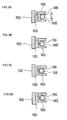
FIG 1 is a schematic view of a conventional polishing apparatus for polishing a periphery of a wafer. As shown inFIG 1 , this type of polishing apparatus has awafer stage unit 120 configured to hold a wafer W, apolishing head 142 configured to press apolishing tape 141 against a periphery of the wafer W, asupply reel 145a for supplying thepolishing tape 141 to thepolishing head 142, and arewind reel 145b for rewinding the usedpolishing tape 141. Thesupply reel 145a and therewind reel 145b are rotated so as to supply and rewind thepolishing tape 141. Thesupply reel 145a and therewind reel 145b are fixed to a stationary member that is part of the polishing apparatus. - The polishing
head 142 has atape transfer mechanism 143 therein. Thistape transfer mechanism 143 has a tape-transferring roller and a holding roller. Thepolishing tape 141 is interposed between the tape-transferring roller and the holding roller, while the tape-transferring roller is rotated to thereby transfer thepolishing tape 141. Thepolishing tape 141 is pulled toward thepolishing head 142 by thetape transfer mechanism 143. A travel direction of thepolishing tape 141 is guided byguide rollers polishing tape 141 is placed in contact with the periphery of the wafer W. After contacting the periphery of the wafer W, thepolishing tape 141 is rewound by therewind reel 145b. Thesupply reel 145a and therewind reel 145b are coupled to non-illustrated motors that provide thepolishing tape 141 with a suitable tension. Thepolishing head 142 performs a linearly-reciprocating motion in vertical directions, as indicated by arrows inFIG 1 , to thereby provide relative movement between thepolishing tape 141 and the wafer W, thus polishing the periphery of the wafer W -
FIG 2 is a plan view illustrating mechanisms for the linearly-reciprocating motion of the polishinghead 142.FIGS. 3A through 3D are views taken along line III-III inFIG 2 . - The polishing
head 142 is fixed to one end of amovable arm 160, and acam shaft 161 is provided at another end of themovable arm 160. Themovable arm 160 is supported by asupport arm 162 vialinear guides 163. Theselinear guides 163 are configured to guide movement of themovable arm 160 so as to allow themovable arm 160 to move linearly relative to thesupport arm 162. A motor M for driving thecam shaft 161 is mounted on thesupport arm 162. This motor M has a rotational shaft coupled to thecam shaft 161 via pulleys p101 and p102 and abelt b 100. The rotational shaft of the motor M and thecam shaft 161 are rotatably supported bybearings support arm 162. Thecam shaft 161 has aneccentric shaft 161 a which is off-centered with respect to a central axis of the bearing 164B. Acam 165 is mounted on a tip end of theeccentric shaft 161a. Thiscam 165 is fitted into agroove 166 of a U-shaped portion of the movable arm 160 (seeFIG 3A ). - As the motor M is energized, the
cam shaft 161 is rotated via the pulleys p101 and p102 and the belt b100. Since theeccentric shaft 161a is rotated eccentrically with its central axis deviating from the central axis of thebearing 164B, thecam 165 is also rotated eccentrically. As shown inFIGS. 3A through 3D , eccentric rotation of thecam 165 in thegroove 166 causes themovable arm 160 to perform a linearly-reciprocating motion in vertical directions, thus causing thepolishing head 142 on the tip end of themovable arm 160 to perform a linearly-reciprocating motion in vertical directions. - The
tape transfer mechanism 143 is operable to transfer thepolishing tape 141 from thesupply reel 145a to therewind reel 145b at a constant speed. On the one hand this tape-transferring speed is very low, and on the other hand a speed of the polishinghead 142 reciprocating linearly is very high. Therefore, in the tape supplying and rewinding operations of thesupply reel 145a and therewind reel 145b, which will be discussed later, the tape-transferring speed is practically negligible as compared with the speed of the reciprocatingpolishing head 142. -
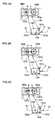
FIGS. 4A through 4C are views illustrating the operations of thepolishing head 142, thesupply reel 145a, and therewind reel 145b. InFIGS. 4A through 4C , reference symbols A and B represent certain points on thepolishing tape 141 attached to thesupply reel 145a and therewind reel 145b. -
FIG 4A shows a state in which a center Ch of the polishinghead 142 is aligned with a thickness center Cw of the wafer W (which will be hereinafter referred to as simply a wafer center). The wafer center Cw is fixed in position during polishing. On the other hand, thepolishing head 142 performs the linearly-reciprocating motion across the wafer center Cw. -
FIG 4B shows a state in which thepolishing head 142 is linearly moved downwardly from the wafer center Cw. During this downward movement, thepolishing tape 141 is pulled from thesupply reel 145a and therewind reel 145b, and the points A and B on thepolishing tape 141 are moved downwardly, as shown inFIG 4B . As a result, thesupply reel 145a and therewind reel 145b are rotated through a certain angle corresponding to a length of thepolishing tape 141 that has been pulled out. -
FIG 4C shows a state in which thepolishing head 142 is linearly moved upwardly from the wafer center Cw. During this upward movement, thepolishing tape 141 is rewound by thesupply reel 145a and therewind reel 145b, and the points A and B on thepolishing tape 141 are moved upwardly, as shown inFIG 4C . As a result, thesupply reel 145a and therewind reel 145b are rotated through a certain angle corresponding to a length of thepolishing tape 141 that has been rewound. In this manner, in accordance with a change in distance between the polishinghead 142 and the supply andrewind reels supply reel 145a and therewind reel 145b repeat supply and rewind of thepolishing tape 141, as shown inFIGS. 4B and 4C . - However, as the
supply reel 145a and therewind reel 145b repeat supply and rewind of thepolishing tape 141, the tension of thepolishing tape 141 would change when the supply and rewind operations are switched, resulting in unstable polishing performance. In particular, as the reciprocating motion becomes faster, an excessive tension could be exerted on thepolishing tape 141 when the supply and rewind operations are switched. As a result, thepolishing tape 141 would be cut or stretch (i.e., permanent strain). On the other hand, the tension of thepolishing tape 141 could be zero when the supply and rewind operations are switched. As a result, thepolishing tape 141 slackens, and a desired polishing performance cannot be obtained. - If the reciprocating speed of the
polishing head 142 can be increased, a removal amount of materials per unit time (i.e., a polishing speed or a removal rate) can be increased. Therefore, the polishing performance of the polishing apparatus can be improved. However, because of the above-described problems, the reciprocating speed of the polishinghead 142 cannot be increased so high. In order to solve such problems, thesupply reel 145a may be incorporated in thepolishing head 142. In this case, however, a motor for providing the polishing tape with a tension becomes heavy. Moreover, if along polishing tape 141 is to be used, thesupply reel 145a is required to be large. This means that the polishinghead 142 and the drive mechanisms for the reciprocating motion are required to be large in size. - Furthermore,
WO 2006 112 530 A andWO 2006 112 532 A both show a polishing apparatus for polishing a workpiece. The polishing apparatus comprises a holding section configured to hold the workpiece, a polishing head configured to bring the polishing tape into contact with the workpiece, a supply reel for the polishing tape to said polishing head, a rewind reel to rewind the polishing tape, and tilting mechanism configured to enable the polishing head to be inclined so that the polishing tape can contact a periphery of a substrate at a certain angle. -
WO 2006 112 532 A shows also a vertical movement mechanism (Figs. 17, 18) configured to cause the polishing head to perform a reciprocating motion to cause the polishing tape to oscillate while contacting the periphery of the substrate. - Attention is also drawn to
US 2004 185 751 A , which shows a substrate processing apparatus used for removing surface irregularities occurring on the peripheral portion of a substrate. The substrate processing apparatus includes an edge-portion polisher for pressing a polishing tape against an edge portion of a substrate and making a relative movement between the polishing tape and the substrate to polish the edge portion of the substrate, and a bevel-portion polisher for pressing a polishing tape against a bevel portion of the substrate and making a relative movement between the polishing tape and the substrate to polish the bevel portion of the substrate. - The present invention has been made in view of the above drawbacks. It is therefore an object of the present invention to provide a polishing apparatus and a polishing method capable of providing a polishing tape with a substantially constant tension during polishing, and capable of improving a removal rate.
- In order to solve the above drawbacks, according to one aspect of the present invention, there is provided a polishing apparatus ad a method for polishing a periphery of a substrate by providing relative movement between a polishing tape and the substrate, as set forth in claims 1 and 9, respectively. The apparatus inter alia includes: a holding section configured to hold the substrate; a polishing head configured to bring the polishing tape into contact with the periphery of the substrate; a supply reel configured to supply the polishing tape to the polishing head; a rewind reel configured to rewind the polishing tape that has contacted the substrate; and a swinging mechanism configured to cause the polishing head to oscillate around a pivot while contacting the periphery of the substrate, wherein the swinging mechanism includes (i) a swing arm to which the polishing head is fixed, (ii) a support arm rotatably coupled to the swing arm via a connecting shaft, and (iii) a drive mechanism configured to cause the swing arm to perform a swinging motion with its pivot lying on a central axis of the connecting shaft.
- In a preferred aspect of the present invention, the polishing tape extends from the supply reel via a pivot of the swinging motion of the polishing head to the substrate.
- In a preferred aspect of the present invention, the pivot of the swinging motion is positioned in the polishing head.
- In a preferred aspect of the present invention, the substrate comprises a semiconductor wafer having a notch portion formed in a periphery thereof; and the polishing head is configured to bring the polishing tape into contact with the notch portion.
- Another aspect of the present invention is to provide a polishing apparatus further including a tilting mechanism configured to tilt the polishing head and the swinging mechanism with respect to a surface of the workpiece.
- In a preferred aspect of the present invention, the tilting mechanism includes (i) a rotatable support shaft supporting the support arm, and (ii) a rotating mechanism configured to rotate the support shaft.
- In a preferred aspect of the present invention, the connecting shaft and the support shaft are arranged in parallel with each other.
- In a preferred aspect of the present invention, the swinging motion of the polishing head comprises rotation of the polishing head in a clockwise direction and a counterclockwise direction alternately through the same angle from a reference line, which intersects the central axis of the connecting shaft and a central axis of the support shaft at a right angle.
- The polishing method inter alia includes holding the substrate; bringing the polishing tape by a polishing head into contact with the periphery of the substrate, while supplying the polishing tape from a supply reel to the polishing head; and swinging the polishing head to cause the polishing tape to oscillate around a pivot while contacting the periphery of the substrate.
- In a preferred aspect of the present invention, the polishing tape extends from the supply reel via a pivot of the swinging motion of the polishing head to the workpiece.
- In a preferred aspect of the present invention, the pivot of the swinging motion is positioned in the polishing head.
- In a preferred aspect of the present invention, the workpiece comprises a semiconductor wafer having a notch portion formed in a periphery thereof; and the bringing the polishing tape by a polishing head into contact with the workpiece comprises bringing the polishing tape by the polishing head into contact with the notch portion.
- In another aspect of the present invention, the polishing method further comprises while swinging the polishing head, tilting the polishing head with respect to a surface of the workpiece.
- In a preferred aspect of the present invention, the polishing tool comprises a polishing tape; and the swinging the polishing head comprises swinging the polishing head while transferring the polishing tape to the workpiece via a pivot of a swinging motion of the polishing head.
- According to the present invention, the swinging motion can be performed at a high speed, while keeping a constant tension of the polishing tape. Therefore, a removal amount of materials per unit time, i.e., a removal rate, can be increased, and as a result, a throughput of the polishing apparatus can be improved.
-
-
FIG 1 is a schematic view showing a conventional polishing apparatus for polishing a periphery of a wafer; -
FIG 2 is a plan view illustrating mechanisms for a linearly-reciprocating motion of a polishing head; -
FIGS. 3A through 3D are views taken along line III-III inFIG 2 ; -
FIGS. 4A through 4C are views illustrating operations of the polishing head, a supply reel, and a rewind reel; -
FIG 5 is a plan view showing a polishing apparatus according to an embodiment of the present invention; -
FIG 6 is a cross-sectional view of the polishing apparatus inFIG 5 ; -
FIG 7 is a plan view showing chuck hands of a wafer-chucking mechanism; -
FIG 8 is a plan view illustrating a swinging mechanism; -
FIGS. 9A through 9D are views each showing a cross-sectional view taken along line IX-IX inFIG 8 ; -
FIGS. 10A through 10C are views for illustrating a tilting motion of a polishing head; -
FIGS. 11A through 11C are views each showing part of the polishing apparatus inFIG 6 ; and -
FIG 12 is a graph showing test results of polishing of a wafer. - Embodiments of the present invention will be described below with reference to the drawings.
-
FIG 5 is a plan view showing a polishing apparatus according to an embodiment of the present invention.FIG 6 is a cross-sectional view of the polishing apparatus inFIG 5 . The polishing apparatus according to the embodiment is suitable for use in polishing of a bevel portion and a notch portion of a periphery of a substrate, such as a semiconductor wafer. The bevel portion is a portion where a right-angled edge in the periphery of the wafer has been removed for the purpose of preventing production of chipped pieces and particles of the wafer. The notch portion is a notch formed in the periphery of the wafer for the purpose of facilitating recognition of an orientation (circumferential position) of the wafer. An example of applications of the present invention will be described below. The below-described embodiment is a polishing apparatus for use in polishing a notch portion of a wafer. - As shown in
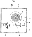
FIGS. 5 and6 , the polishing apparatus according to the embodiment includes a wafer stage unit (substrate holding section) 20 having awafer stage 23 for holding a wafer W, astage moving mechanism 30 for moving thewafer stage unit 20 in directions parallel with an upper surface (a wafer holding surface) of thewafer stage 23, and anotch polishing unit 40 for polishing a notch portion V of the wafer W held by thewafer stage 23. - The
wafer stage unit 20, thestage moving mechanism 30, and thenotch polishing unit 40 are accommodated in ahousing 11. Thishousing 11 has an internal space divided by apartition plate 14 into two spaces: an upper chamber (polishing room) 15 and a lower chamber (machine room) 16. Thewafer stage 23 and thenotch polishing unit 40 are located in theupper chamber 15, and thestage moving mechanism 30 is located in thelower chamber 16. Theupper chamber 15 has a side wall with anopening 12, which can be closed by ashutter 13 that is driven by a non-illustrated air cylinder. - The wafer W is transferred into and out from the
housing 11 through theopening 12. Transferring of the wafer W is performed by a known transfer mechanism (not shown in the drawings) such as a transfer robot.Grooves 26 are formed on the upper surface of thewafer stage 23. Thesegrooves 26 communicate with a non-illustrated vacuum pump via a vertically-extendinghollow shaft 27. As the vacuum pump is driven, vacuum is formed in thegrooves 26, so that the wafer W is held on the upper surface of thewafer stage 23. Thehollow shaft 27 is rotatably supported bybearings 28, and is coupled to a motor m1 via pulleys p1 and p2 and a belt b1. With these arrangements, the wafer W is rotated by the motor m1 with its lower surface being held on the upper surface of thewafer stage 23. - The polishing apparatus further includes a wafer-chucking
mechanism 80 arranged in thehousing 11. This wafer-chuckingmechanism 80 is operable to: receive the wafer W in thehousing 11 from the above-described wafer transfer mechanism; place the wafer W onto thewafer stage 23; and remove the wafer W from thewafer stage 23 to the wafer transfer mechanism. InFIG 5 , only part of the wafer-chuckingmechanism 80 is depicted. -
FIG 7 is a plan view showing chuck hands of the wafer-chucking mechanism. As shown inFIG 7 , the wafer-chuckingmechanism 80 has afirst chuck hand 81 havingpins 83 thereon and asecond chuck hand 82 havingpins 83 thereon. These first and second chuck hands 81 and 82 are driven by a non-illustrated open-close mechanism so as to move closer to and away from each other (as indicated by arrows T). A chuck moving mechanism (not shown in the drawings) is further provided so as to move the first and second chuck hands 81 and 82 in directions perpendicular to the surface of the wafer W held on thewafer stage 23. - A
hand 73 of the wafer transfer mechanism is operable to transfer the wafer W to a position between the first and second chuck hands 81 and 82. Then, the first and second chuck hands 81 and 82 are moved closer to each other to bring thepins 83 into contact with the periphery of the wafer W, whereby the wafer W is clamped by the first and second chuck hands 81 and 82. In this state, a center of the wafer W and a center of the wafer stage 23 (i.e., a rotational axis of the wafer stage 23) are aligned with each other. Therefore, the first and second chuck hands 81 and 82 can function as a centering mechanism. - As shown in
FIG 6 , thestage moving mechanism 30 includes acylindrical bearing base 29 for rotatably supporting thehollow shaft 27, asupport plate 32 on which thebearing base 29 is mounted, amovable plate 33 movable integrally with thesupport plate 32, a ball screw b2 coupled to themovable plate 33, and a motor m2 adapted to rotate the ball screw b2. Themovable plate 33 is coupled to a lower surface of thepartition plate 14 vialinear guides 35, so that themovable plate 33 is movable in directions parallel with the upper surface of thewafer stage 23. The bearingbase 29 extends through a through-hole 17 formed in thepartition plate 14. The above-described motor m1 for rotating thehollow shaft 27 is mounted on thesupport plate 32. - With these arrangements, when the motor m2 rotates the ball screw b2, the
movable plate 33, the bearingbase 29 and thehollow shaft 27 are moved along a longitudinal direction of the linear guides 35. As a result, thewafer stage 23 is moved in directions parallel to the upper surface thereof. InFIG 6 , the movement direction of thewafer stage 23 by thestage moving mechanism 30 is indicated by arrow X. - As shown in
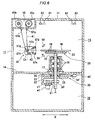
FIG 6 , thenotch polishing unit 40 includes a polishingtape 41, a polishinghead 42 configured to press the polishingtape 41 against the notch portion V of the wafer W, asupply reel 45a configured to supply the polishingtape 41 to the polishinghead 42, and arewind reel 45b configured to rewind the polishingtape 41 that has been supplied to the polishinghead 42. Thesupply reel 45a and therewind reel 45b are housed in areel chamber 46 provided on thehousing 11. Thesupply reel 45a and therewind reel 45b are fixed in position. - The polishing
head 42 has atape transfer mechanism 43 therein. Thistape transfer mechanism 43 includes a tape-transferring roller and a holding roller. The polishingtape 41 is interposed between the tape-transferring roller and the holding roller, while the tape-transferring roller is rotated to thereby transfer the polishingtape 41. The polishingtape 41 is pulled out from thesupply reel 45a by thetape transfer mechanism 43, and is directed to the polishinghead 42 via aguide roller 57a. The polishinghead 42 is operable to bring a polishing surface of the polishingtape 41 into contact with the notch portion V of the wafer W After contacting the notch portion V, the polishingtape 41 is rewound by therewind reel 45b via aguide roller 57b. As shown inFIG 6 , polishing-liquid supply nozzles 58 are arranged above and below the wafer W, so that a polishing liquid (typically pure water) or cooling water can be supplied onto a contact portion between the wafer W and the polishingtape 41. - The polishing
head 42 hasguide rollers tape 41. The polishinghead 42 is configured to perform a swinging motion (an oscillating motion) with its pivot lying on a lower end point Cn of theguide roller 57c (i.e., a lowermost end of a outer circumferential surface of theguide roller 57c). More specifically, the polishinghead 42 rotates about the point Cn on theguide roller 57c) through a predetermined angle by a swinging mechanism, which will be described below. In the following descriptions, the lower end point Cn of theguide roller 57c will be referred to as a pivot (a center of the swinging motion) Cn. -
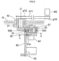
FIG 8 is a plan view illustrating the swinging mechanism, andFIGS. 9A through 9D are views each showing a cross-sectional view taken along line IX-IX inFIG 8 . - As shown in
FIG 8 , the swinging mechanism includes aswing arm 60 to which the polishinghead 42 is fixed, asupport arm 62 supporting theswing arm 60, a connectingarm 67 coupling theswing arm 60 and thesupport arm 62 to each other, and a drive mechanism adapted to swing theswing arm 60. This drive mechanism includes a cam shaft (crank shaft) 61 having aneccentric shaft 61a, acam 65 fixed to thecam shaft 61, and a motor M1 serving as a drive source for rotating thecam shaft 61. - The polishing
head 42 is mounted on one end of theswing arm 60, and thecam shaft 61 is arranged at another end of theswing arm 60. The connectingshaft 67 is fixed to theswing arm 60 and is rotatably supported by a bearing 64A mounted on thesupport arm 62, so that theswing arm 60 is rotatable about the connectingshaft 67. The above-mentioned pivot Cn is positioned on a central axis Ln of the connectingshaft 67. The motor M1 is fixed to thesupport arm 62, and a rotational shaft of the motor M 1 is coupled to thecam shaft 61 via pulleys p11 and p12 and a belt b10. Thecam shaft 61 is rotatably supported by a bearing 64B mounted on thesupport arm 62. Theeccentric shaft 61 a of thecam shaft 61 is off-centered with respect to a central axis of the bearing 64B. Thecam 65 is mounted on a tip end of theeccentric shaft 61a. Thiscam 65 is fitted into agroove 66 of a U-shaped portion of the swing arm 60 (seeFIG 9A ). - As the motor M1 is energized, the
cam shaft 61 is rotated via the pulleys p11 and p12 and the belt b10. Since theeccentric shaft 61a is rotated eccentrically with its central axis deviating from the central axis of the bearing 64B, thecam 65 is also rotated eccentrically. As shown inFIGS. 9A through 9D , eccentric rotation of thecam 65 in thegroove 66 causes theswing arm 60 to perform a swinging motion on the central axis of the connectingshaft 67. As described above, the central axis Ln of the connectingshaft 67 is aligned with the pivot Cn as shown inFIG 6 . Therefore, the polishinghead 42, mounted on the tip end of theswing arm 60, performs the swinging motion on the pivot Cn. In the specification, the swinging motion means rotation about a point (the pivot Cn in this embodiment) in a clockwise direction and a counterclockwise direction alternately through a certain angle. - As shown in
FIG 8 , thesupport arm 62 is rotatable about asupport shaft 90 fixed thereto so that the polishinghead 42 and the swinging mechanism are integrally tilted with respect to a surface of the wafer W. Thesupport shaft 90 extends in parallel with the connectingshaft 67, and is rotatably supported by a bearing 91 mounted on astationary member 95. Thesupport shaft 90 is coupled to a motor M2 serving as a drive source via pulleys p13 and p14 and a belt b11. A polishing point (a contact point between the polishingtape 41 and the wafer W) is on a central axis Lt of thesupport shaft 90. Therefore, the polishinghead 42 and the swinging mechanism are rotated (i.e., tilted) about the polishing point by rotation of thesupport shaft 90 driven by the motor M2. In this embodiment, a tilting mechanism for tilting the polishinghead 42 is constituted by thesupport shaft 90, the pulleys p13 and p14, the belt b11, and the motor M2. - As shown in
FIGS. 9A through 9C , a rotational angle θ of the polishinghead 42 in the clockwise direction is equal to a rotational angle θ in the counterclockwise direction. More specifically, the polishinghead 42 makes the clockwise rotation and counterclockwise rotation through the same angle θ from a reference line Lr. This reference line Lr is defined as a line that intersects the central axis Ln of theconnection shaft 67 and the central axis Lt of thesupport shaft 90 at a right angle. Even when the polishinghead 42 is tilted by the tilting mechanism, the swinging motion of the polishinghead 42 is performed as well. -
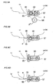
FIGS. 10A through 10C are views for illustrating tilting motion of the polishinghead 42. More specifically,FIG 10A shows a state in which the pivot Cn of the polishinghead 42 is aligned with the center Cw of the wafer W,FIG 10B shows a state in which the polishinghead 42 is tilted upwardly, andFIG 10C shows a state in which the polishinghead 42 is tilted downwardly. - Since the
swing arm 60 and the polishinghead 42 are tilted integrally with thesupport arm 62, the pivot Cn of the swinging motion is positioned in the polishinghead 42 at all times, regardless of a tilting angle of the polishinghead 42. Therefore, even when the polishinghead 42 is tilted, the polishinghead 42 can perform the swinging motion on the pivot Cn. In this swinging motion, the polishinghead 42 makes the clockwise rotation and counterclockwise rotation about the pivot Cn through the same angle, regardless of an angle of the polishinghead 42 tilted. - The polishing
tape 41, supplied from thesupply reel 45a, is guided by theguide roller 57a and theguide roller 57c so as to extend via the pivot Cn to theguide roller 57d and theguide roller 57e which are provided on a front end of the polishinghead 42. Theguide roller 57d is arranged above theguide roller 57e. The travel direction of the polishingtape 41 is guided by theseguide roller 57d and theguide roller 57e so that the polishingtape 41 contacts the wafer W. - The
supply reel 45a and therewind reel 45b are coupled to non-illustrated motors that provide the polishingtape 41 with a suitable tension, so that the polishingtape 41 does not slacken. Thetape transfer mechanism 43 is operable to transfer the polishingtape 41 from thesupply reel 45a to therewind reel 45b at a constant speed. This tape-transferring speed is several millimeters to tens of millimeters per minute. On the other hand, a swinging speed of the polishinghead 42 is as high as several hundred times per minute. Therefore, the tape-transferring speed is practically negligible as compared with the swinging speed of the polishinghead 42. - The polishing
tape 41 may comprise a base film having a polishing surface to which abrasive particles, such as diamond particles or SiC particles, are attached. The abrasive particles to be attached to the polishingtape 41 are selected in accordance with a type of wafer and a polishing performance required. For example, the abrasive particles may be diamond particles or SiC particles having an average diameter in a range of 0.1 µm to 5.0 µm. The polishingtape 42 may be a belt-shaped polishing cloth with no abrasive particles. The base film may comprise a film made from a flexible material, such as polyester, polyurethane, or polyethylene terephthalate. - Next, operations of the polishing apparatus having the above-described structures will be described. The wafer W is transferred by the non-illustrated wafer transfer mechanism into the
housing 11 through theopening 12. The wafer-chuckingmechanism 80 receives the wafer W from the hand 73 (seeFIG 7 ) of the wafer transfer mechanism, and clamps the wafer W by the first and second chuck hands 81 and 82. After the first and second chuck hands 81 and 82 receives the wafer W, thehand 73 of the wafer transfer mechanism is removed from thehousing 11, and then theshutter 13 is closed. The wafer-chuckingmechanism 80 is moved downwardly to lower the wafer W and place the wafer W onto the upper surface of thewafer stage 23. Then, the non-illustrated vacuum pump operates to attract the wafer W to the upper surface of thewafer stage 23. - The
wafer stage 23, holding the wafer W, is moved by thestage moving mechanism 30 to a position near the polishinghead 42. The motor m1 is energized to rotate thewafer stage 23 so that the notch portion V of the wafer W faces the polishinghead 42. Then, the polishing liquid is supplied to the wafer W from the polishingliquid supply nozzles 58. After a flow rate of the polishing liquid as supplied reaches a predetermined value, the wafer W is moved by thestage moving mechanism 30 until the wafer W is brought into contact with the polishingtape 41. Then, the swinging mechanism operates to cause the polishinghead 42 to perform the swinging motion. As a result, the polishingtape 41 oscillates in directions perpendicular to the surface of the wafer W, and the polishing surface of the polishingtape 41 is placed in sliding contact with the notch portion V In this manner, the notch portion V of the wafer W is polished. Further, the polishinghead 42 is tilted so that the polishingtape 41 contacts the wafer W at varying angles, whereby the notch portion V in its entirety is polished from its upper surface to its lower surface. -
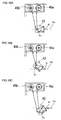
FIGS. 11A through 11C are views each showing part of the polishing apparatus shown inFIG 6 . Hereinafter, operations of the polishinghead 42, thesupply reel 45a, and therewind reel 45b when the polishinghead 42 is performing the swinging motion will be described with reference toFIGS. 11A through 11C . InFIGS. 11A through 11C , reference symbols A and B represent certain points on the polishingtape 41 attached to thesupply reel 45a and therewind reel 45b. As described above, the transferring speed of the polishingtape 41 is practically negligible as compared with the speed of the swinging motion of the polishinghead 42. Therefore, the following descriptions assume that the transferring speed of the polishingtape 41 is zero. -
FIG 11A illustrates a state in which the pivot Cn lies in the same plane as the center line (the center in thickness direction) Cw of the wafer W. As indicated by arrows, the polishinghead 42 performs the swinging motion on the pivot Cn that is located in the polishinghead 42. Therefore, a distance between thesupply reel 45a and the pivot Cn is constant at all times, regardless of whether the polishinghead 42 is performing the swinging motion. -
FIG 11B illustrates a state in which the front end of the polishinghead 42 moves upwardly during the swinging motion. During this upward movement, the length of the polishingtape 41 that lies between thesupply reel 45a and theguide roller 57c on the pivot Cn does not substantially change. The length of the polishingtape 41 that lies between theguide roller 57c and theguide roller 57d arranged on the front end of the polishinghead 42 does not substantially change as well. Therefore, as can be seen fromFIGS. 11A and 11B , the point A at the supply-reel side stays substantially in its original position, and the point B at the rewind-reel side moves slightly. -
FIG 11C illustrates a state in which the front end of the polishinghead 42 moves downwardly during the swinging motion. During this downward movement, the length of the polishingtape 41 that lies between thesupply reel 45a and theguide roller 57c on the pivot Cn does not substantially change. The length of the polishingtape 41 that lies between theguide roller 57c and theguide roller 57d does not substantially change as well. Therefore, as can be seen fromFIGS. 11A and 11C , the point A at the supply-reel side stays substantially in its original position, and the point B at the rewind-reel side moves slightly. - As shown in
FIGS. 11B and 11C , the swinging motion of the polishinghead 42 provides relative movement between the wafer W and the polishingtape 41 on the front end of the polishinghead 42. During this movement, the position of the point A on the polishingtape 41 does not substantially change. - Because the polishing
tape 41 is clamped by thetape transfer mechanism 43, the tension of the polishingtape 41, which is important for the polishing performance, is maintained in the region between thetape transfer mechanism 43 and thesupply reel 45a. Therefore, theguide rollers guide rollers tape 41. For example, theguide rollers tape 41 does not slacken too much and does not come off the guide rollers. In order to reduce the movement of the point B at the rewind-reel side, it is preferable that theguide rollers tape 41 is returned to therewind reel 45b via a certain point as near to the pivot Cn as possible. - In the regions between the polishing
head 42 and the supply andrewind reels tape 41 hardly move or slightly move. Therefore, the tension of the polishingtape 41 can be stable, compared with the conventional linearly-reciprocating motion that causes rewinding and pulling of the polishing tape repetitively. Even when the swinging motion is performed at a high speed, an excessive tension is not applied to the polishingtape 41 when the polishinghead 42 switches its movement direction. Hence, a stable polishing performance can be maintained. Furthermore, cutting or elongation (permanent strain) of the polishingtape 41 is unlikely to occur. In addition, the tension of the polishingtape 41 does not become zero, and the polishingtape 41 does not slacken. -
FIG. 12 is a graph showing an example of measurement results of the tension applied to the polishing tape when the polishing head performs the linearly-reciprocating motion (prior art) and the swinging motion (present invention). A horizontal axis shows time, and a vertical axis shows percentage that indicates actual tension of the polishing tape with respect to a preset tension as 100%. The tension was measured using a tension sensor which is commercially available. -
FIG 12 shows data that were obtained from a test that was conducted on condition that the linearly-reciprocating motion and the swinging motion of the polishing head were both performed at 300 cycles per minute. As can be seen fromFIG 12 , the tension in the linearly-reciprocating motion fluctuates widely due to repetition of pulling and rewinding of the polishing tape. This is because of not only an influence of switching of the directions of the linearly-reciprocating motion, but also an influence of rolling friction resulting from a change in rotating direction of the guide rollers. On the other hand, as can be seen fromFIG 12 , the tension in the swinging motion according to the present invention does not fluctuate widely and is stable. This is because the swinging motion of the polishinghead 42 causes little movement of the polishingtape 41. As a result, the tape pulling and rewinding operations and the rolling friction of the guide rollers do not exert an influence on the tension of the polishing tape. - Test was further conducted on condition that both the linearly-reciprocating motion and the swinging motion of the polishing head were performed at 500 cycles per minute. This test showed that the linearly-reciprocating motion resulted in wide fluctuation in tape tension, but the swinging motion still resulted in little fluctuation in tape tension. The test results confirmed that relative speed between the polishing tape and the wafer can be increased and that the removal rate can thus be increased greatly.
- Further, a time required to remove an oxide film on a notch portion of a silicon wafer having the oxide film thereon with a thickness of 100 nm was measured. As a result, the conventional polishing head performing the linearly-reciprocating motion needed 28 seconds. On the other hand, the polishing head performing the swinging motion needed 15 seconds to completely remove the oxide film. These experiments were conducted under the condition that the polishing head operated at 300 cycles per minute. When the polishing head performed the swinging motion at 500 cycles per minute, stable polishing of a wafer was still achieved. In this case, it took at most 10 seconds to completely remove the oxide film. In addition, inspection test results showed that deep scratches were less formed on the polished surface. This seems to be due to the fact that the fluctuation of the tension was small, and a large load was not applied at peaks of the fluctuation.
- As described above, according to the present invention, the swinging motion can be performed at a high speed, while maintaining a stable polishing performance. Therefore, a removal amount per unit time, i.e., a removal rate, can be increased, and as a result, a throughput of the polishing apparatus can be improved.
- The previous description of embodiments is provided to enable a person skilled in the art to make and use the present invention. Moreover, various modifications to these embodiments will be readily apparent to those skilled in the art, and the generic principles and specific examples defined herein may be applied to other embodiments. Therefore, the present invention is not intended to be limited to the embodiments described herein but is to be accorded the widest scope as defined by limitation of the claims.
Claims (13)
- A polishing apparatus for polishing a periphery of a substrate by providing relative movement between a polishing tape (41) and the substrate, said apparatus comprising:a holding section (20) configured to hold the substrate;a polishing head (42) configured to bring the polishing tape (41) into contact with the periphery of the substrate;a supply reel (45a) configured to supply the polishing tape (41) to said polishing head (42);a rewind reel (45b) configured to rewind the polishing tape (41) that has contacted the substrate;characterized bya swinging mechanism (60, 62 , 67, M1) configured to cause said polishing head (42) to perform a swinging motion to cause the polishing tape (41) to oscillate while contacting the periphery of the substrate,wherein said swinging mechanism includes:a swing arm (60) to which said polishing head (42) is fixed,a connecting shaft (67),a support arm (62) rotatably coupled to said swing arm (60) via said connecting shaft (67), anda drive mechanism (M1, 61, 65) configured to cause said swing arm (60) to perform the swinging motion with its pivot lying on a central axis (Ln) of said connecting shaft (67).
- The polishing apparatus according to claim 1, wherein the polishing tape (41) extends from said supply reel (45a) to the substrate via the pivot of the swinging motion of said polishing head (42).
- The polishing apparatus according to claim 1 or 2, wherein the pivot of the swinging motion is positioned in said polishing head (42).
- The polishing apparatus according to any one of the preceding claims, wherein:the substrate comprises a semiconductor wafer having a notch portion formed in the periphery thereof; andsaid polishing head (42) is configured to bring the polishing tape (41) into contact with the notch portion.
- The polishing apparatus according to any one of the preceding claims, further comprising a tilting mechanism (M2, 90) configured to tilt said polishing head (42) and said swinging mechanism (60, 62 , 67, M1) with respect to a surface of the substrate.
- The polishing apparatus according to claim 5, wherein said tilting mechanism (M2, 90) includes:(i) a rotatable support shaft (90) supporting said support arm (62), and(ii) a rotating mechanism (M2, p13, p14, b11) configured to rotate said support shaft (90).
- The polishing apparatus according to claim 6, wherein said connecting shaft (67) and said support shaft (90) are arranged in parallel with each other.
- The polishing apparatus according to claim 7, wherein the swinging motion of said polishing head (42) comprises rotation of said polishing head (42) in a clockwise direction and a counterclockwise direction alternately through the same angle from a reference line, which intersects the central axis of said connecting shaft (67) and a central axis of said support shaft (90) at a right angle.
- A polishing method of polishing a periphery of a substrate using a polishing apparatus according to any of claims 1 to 8, said method comprising:providing relative movement between a polishing tape (41) and the substrate;holding the substrate;bringing the polishing tape (41) by the polishing head (42) into contact with the periphery of the substrate, while supplying the polishing tape (41) from the supply reel (45a) to the polishing head (42); andswinging the polishing head (42) to cause the polishing tape (41) to oscillate around the pivot while contacting the periphery of the substrate.
- The polishing method according to claim 9, wherein the polishing tape (41) extends from the supply reel (45a) to the substrate via a pivot of the swinging motion of the polishing head (42).
- The polishing method according to claim 9 or 10, wherein a pivot of the swinging motion is positioned in the polishing head (42).
- The polishing method according to any one of claims 9 to 11, wherein:the substrate comprises a semiconductor wafer having a notch portion formed in the periphery thereof; andsaid bringing the polishing tape (41) by the polishing head (42) into contact with the periphery of the substrate comprises bringing the polishing tape (41) by the polishing head (42) into contact with the notch portion.
- The polishing method according to any one of claims 9 to 12, further comprising while swinging the polishing head (42), tilting the polishing head (42) with respect to a surface of the substrate.
Applications Claiming Priority (1)
| Application Number | Priority Date | Filing Date | Title |
|---|---|---|---|
| JP2007171959 | 2007-06-29 |
Publications (2)
| Publication Number | Publication Date |
|---|---|
| EP2008769A1 EP2008769A1 (en) | 2008-12-31 |
| EP2008769B1 true EP2008769B1 (en) | 2011-03-02 |
Family
ID=39816648
Family Applications (1)
| Application Number | Title | Priority Date | Filing Date |
|---|---|---|---|
| EP08011343A Active EP2008769B1 (en) | 2007-06-29 | 2008-06-23 | Polishing apparatus and polishing method |
Country Status (7)
| Country | Link |
|---|---|
| US (1) | US7976361B2 (en) |
| EP (1) | EP2008769B1 (en) |
| JP (2) | JP5188285B2 (en) |
| KR (1) | KR101488993B1 (en) |
| CN (1) | CN101332580B (en) |
| DE (1) | DE602008005211D1 (en) |
| TW (1) | TWI436852B (en) |
Families Citing this family (21)
| Publication number | Priority date | Publication date | Assignee | Title |
|---|---|---|---|---|
| US8892238B2 (en) * | 2009-10-06 | 2014-11-18 | Edward T. Sweet | Edge break details and processing |
| US20110081839A1 (en) * | 2009-10-06 | 2011-04-07 | Apple Inc. | Method and apparatus for polishing a curved edge |
| JP5182317B2 (en) * | 2010-03-31 | 2013-04-17 | ブラザー工業株式会社 | lens |
| CN101934489B (en) * | 2010-07-30 | 2012-10-03 | 溧阳市四方不锈钢制品有限公司 | Grinding machine for tube strip weld joint |
| JP5649417B2 (en) * | 2010-11-26 | 2015-01-07 | 株式会社荏原製作所 | Substrate polishing method using polishing tape having fixed abrasive grains |
| US8540551B2 (en) * | 2010-12-15 | 2013-09-24 | Corning Incorporated | Glass edge finish system, belt assembly, and method for using same |
| CN102233536A (en) * | 2011-05-10 | 2011-11-09 | 淄博隆嘉工贸有限公司 | Automatic polishing machine for ceramic moveable mould |
| TWI663018B (en) * | 2012-09-24 | 2019-06-21 | 日商荏原製作所股份有限公司 | Grinding method and grinding device |
| US9339912B2 (en) | 2013-01-31 | 2016-05-17 | Taiwan Semiconductor Manufacturing Company, Ltd. | Wafer polishing tool using abrasive tape |
| JP6071611B2 (en) * | 2013-02-13 | 2017-02-01 | Mipox株式会社 | Method for manufacturing circular wafer by polishing peripheral edge of wafer made of crystalline material having notch portion such as orientation flat using polishing tape |
| JP2015000451A (en) * | 2013-06-17 | 2015-01-05 | ワイエイシイ株式会社 | Apparatus for processing substrate surface |
| JP6113624B2 (en) * | 2013-10-11 | 2017-04-12 | 株式会社荏原製作所 | Substrate processing apparatus and substrate processing method |
| CN105196140B (en) * | 2015-10-20 | 2017-05-31 | 慈溪市华表机械有限公司 | A kind of external cylindrical superfinishing machine |
| EP3335832B1 (en) * | 2016-12-15 | 2021-02-03 | Ebara Corporation | Polishing apparatus and pressing pad for pressing polishing tool |
| JP6920849B2 (en) * | 2017-03-27 | 2021-08-18 | 株式会社荏原製作所 | Substrate processing method and equipment |
| JP6974067B2 (en) * | 2017-08-17 | 2021-12-01 | 株式会社荏原製作所 | Methods and equipment for polishing substrates |
| JP7129166B2 (en) * | 2018-01-11 | 2022-09-01 | 株式会社荏原製作所 | SUBSTRATE PROCESSING APPARATUS AND CONTROL METHOD |
| JP7226711B2 (en) * | 2019-02-28 | 2023-02-21 | 範多機械株式会社 | Knocking device |
| CN111745504B (en) * | 2020-05-20 | 2022-06-21 | 深圳市裕展精密科技有限公司 | Polishing mechanism, polishing device and polishing method |
| CN111941201B (en) * | 2020-08-21 | 2021-12-07 | 许昌学院 | High-precision manufacturing device for Fabry-Perot interferometer mirror plate |
| CN114619338A (en) * | 2022-03-28 | 2022-06-14 | 坦龙环保设备南通有限公司 | Street sweeper hydraulic stem apparatus for producing |
Family Cites Families (20)
| Publication number | Priority date | Publication date | Assignee | Title |
|---|---|---|---|---|
| JP2837342B2 (en) * | 1993-12-13 | 1998-12-16 | 日本ミクロコーティング株式会社 | Polishing equipment |
| JP3081140B2 (en) | 1995-09-21 | 2000-08-28 | 日本ミクロコーティング株式会社 | Polishing device with polishing tape |
| NO306765B1 (en) * | 1998-04-03 | 1999-12-20 | Grobi As | Device for rounding holes in a workpiece |
| US6685539B1 (en) * | 1999-08-24 | 2004-02-03 | Ricoh Company, Ltd. | Processing tool, method of producing tool, processing method and processing apparatus |
| US6629875B2 (en) * | 2000-01-28 | 2003-10-07 | Accretech Usa, Inc. | Machine for grinding-polishing of a water edge |
| JP4156200B2 (en) * | 2001-01-09 | 2008-09-24 | 株式会社荏原製作所 | Polishing apparatus and polishing method |
| JP2003220546A (en) * | 2002-01-24 | 2003-08-05 | Soken Kogyo Kk | Belt type polishing device |
| JP4090247B2 (en) * | 2002-02-12 | 2008-05-28 | 株式会社荏原製作所 | Substrate processing equipment |
| JP4125148B2 (en) | 2003-02-03 | 2008-07-30 | 株式会社荏原製作所 | Substrate processing equipment |
| CN100429752C (en) * | 2004-02-25 | 2008-10-29 | 株式会社荏原制作所 | Polishing apparatus and substrate processing apparatus |
| WO2006041196A1 (en) * | 2004-10-15 | 2006-04-20 | Kabushiki Kaisha Toshiba | Polishing apparatus and polishing method |
| JP2006142388A (en) * | 2004-11-16 | 2006-06-08 | Nihon Micro Coating Co Ltd | Abrasive tape and method |
| EP1872392B1 (en) | 2005-04-19 | 2012-02-22 | Ebara Corporation | Substrate processing apparatus |
| CN100585812C (en) | 2005-04-19 | 2010-01-27 | 株式会社荏原制作所 | Substrate processing apparatus |
| JP5196709B2 (en) * | 2005-04-19 | 2013-05-15 | 株式会社荏原製作所 | Semiconductor wafer peripheral polishing apparatus and method |
| EP1976806A4 (en) * | 2005-12-09 | 2011-08-10 | Applied Materials Inc | Methods and apparatus for processing a substrate |
| US7993485B2 (en) * | 2005-12-09 | 2011-08-09 | Applied Materials, Inc. | Methods and apparatus for processing a substrate |
| JP2009532210A (en) * | 2006-03-30 | 2009-09-10 | アプライド マテリアルズ インコーポレイテッド | Method and apparatus for polishing an edge of a substrate |
| JP2008036783A (en) * | 2006-08-08 | 2008-02-21 | Sony Corp | Grinding method and grinding device |
| JP2008284684A (en) * | 2007-05-21 | 2008-11-27 | Applied Materials Inc | Method and apparatus for polishing edge of substrate using polishing arm |
-
2008
- 2008-06-16 US US12/213,186 patent/US7976361B2/en active Active
- 2008-06-19 TW TW097122820A patent/TWI436852B/en active
- 2008-06-19 JP JP2008160380A patent/JP5188285B2/en active Active
- 2008-06-23 EP EP08011343A patent/EP2008769B1/en active Active
- 2008-06-23 DE DE602008005211T patent/DE602008005211D1/en active Active
- 2008-06-27 CN CN2008101285883A patent/CN101332580B/en active Active
- 2008-06-27 KR KR20080061705A patent/KR101488993B1/en active IP Right Grant
-
2012
- 2012-12-14 JP JP2012273699A patent/JP5525590B2/en active Active
Also Published As
| Publication number | Publication date |
|---|---|
| EP2008769A1 (en) | 2008-12-31 |
| TW200932423A (en) | 2009-08-01 |
| CN101332580A (en) | 2008-12-31 |
| JP5188285B2 (en) | 2013-04-24 |
| CN101332580B (en) | 2012-05-09 |
| US20090004952A1 (en) | 2009-01-01 |
| JP5525590B2 (en) | 2014-06-18 |
| DE602008005211D1 (en) | 2011-04-14 |
| TWI436852B (en) | 2014-05-11 |
| JP2009028892A (en) | 2009-02-12 |
| JP2013075358A (en) | 2013-04-25 |
| KR101488993B1 (en) | 2015-02-02 |
| KR20090004590A (en) | 2009-01-12 |
| US7976361B2 (en) | 2011-07-12 |
Similar Documents
| Publication | Publication Date | Title |
|---|---|---|
| EP2008769B1 (en) | Polishing apparatus and polishing method | |
| US9457447B2 (en) | Polishing apparatus and polishing method | |
| US8393935B2 (en) | Polishing apparatus | |
| EP2502701B1 (en) | Polishing apparatus and polishing method | |
| US8047896B2 (en) | Polishing apparatus, polishing method, and processing apparatus | |
| US10414013B2 (en) | Polishing method and polishing apparatus | |
| JP2009154285A (en) | Polishing device and method | |
| US20080293334A1 (en) | Methods and apparatus for using a bevel polishing head with an efficient tape routing arrangement | |
| TWI820076B (en) | Substrate processing device and control method | |
| TWI433754B (en) | Grinding device | |
| US6638147B2 (en) | Polishing method for removing corner material from a semi-conductor wafer | |
| JPH0976148A (en) | Device for polishing notch part of wafer | |
| JP3404579B2 (en) | Polishing device for both shafts | |
| JP3542815B2 (en) | Wafer notch mirror polishing apparatus and mirror polishing method | |
| JP3888618B2 (en) | Rod end face processing equipment | |
| JP7296864B2 (en) | Polishing device and polishing method | |
| WO2009011408A1 (en) | Polishing apparatus | |
| JPH1040508A (en) | Processing device for sliding surface of magnetic head and method therefor | |
| JP2004174629A (en) | Chamfering device for metal belt ring | |
| KR200208032Y1 (en) | Micro superfinishing with linear motion guide | |
| JP2004243470A (en) | Chamfering device of work | |
| JP5360726B2 (en) | Plate member polishing equipment | |
| JP2003007657A (en) | Mirror-surface polisher for wafer notch, and mirror- surface polishing method |
Legal Events
| Date | Code | Title | Description |
|---|---|---|---|
| PUAI | Public reference made under article 153(3) epc to a published international application that has entered the european phase |
Free format text: ORIGINAL CODE: 0009012 |
|
| AK | Designated contracting states |
Kind code of ref document: A1 Designated state(s): AT BE BG CH CY CZ DE DK EE ES FI FR GB GR HR HU IE IS IT LI LT LU LV MC MT NL NO PL PT RO SE SI SK TR |
|
| AX | Request for extension of the european patent |
Extension state: AL BA MK RS |
|
| 17P | Request for examination filed |
Effective date: 20090624 |
|
| 17Q | First examination report despatched |
Effective date: 20090722 |
|
| AKX | Designation fees paid |
Designated state(s): DE |
|
| GRAP | Despatch of communication of intention to grant a patent |
Free format text: ORIGINAL CODE: EPIDOSNIGR1 |
|
| GRAS | Grant fee paid |
Free format text: ORIGINAL CODE: EPIDOSNIGR3 |
|
| GRAA | (expected) grant |
Free format text: ORIGINAL CODE: 0009210 |
|
| AK | Designated contracting states |
Kind code of ref document: B1 Designated state(s): DE |
|
| REF | Corresponds to: |
Ref document number: 602008005211 Country of ref document: DE Date of ref document: 20110414 Kind code of ref document: P |
|
| REG | Reference to a national code |
Ref country code: DE Ref legal event code: R096 Ref document number: 602008005211 Country of ref document: DE Effective date: 20110414 |
|
| PLBE | No opposition filed within time limit |
Free format text: ORIGINAL CODE: 0009261 |
|
| STAA | Information on the status of an ep patent application or granted ep patent |
Free format text: STATUS: NO OPPOSITION FILED WITHIN TIME LIMIT |
|
| 26N | No opposition filed |
Effective date: 20111205 |
|
| REG | Reference to a national code |
Ref country code: DE Ref legal event code: R097 Ref document number: 602008005211 Country of ref document: DE Effective date: 20111205 |
|
| P01 | Opt-out of the competence of the unified patent court (upc) registered |
Effective date: 20230517 |
|
| PGFP | Annual fee paid to national office [announced via postgrant information from national office to epo] |
Ref country code: DE Payment date: 20230502 Year of fee payment: 16 |