EP2001602B1 - Lithography imprinting system - Google Patents
Lithography imprinting system Download PDFInfo
- Publication number
- EP2001602B1 EP2001602B1 EP07754579A EP07754579A EP2001602B1 EP 2001602 B1 EP2001602 B1 EP 2001602B1 EP 07754579 A EP07754579 A EP 07754579A EP 07754579 A EP07754579 A EP 07754579A EP 2001602 B1 EP2001602 B1 EP 2001602B1
- Authority
- EP
- European Patent Office
- Prior art keywords
- template
- substrate
- nano
- recited
- air bearing
- Prior art date
- Legal status (The legal status is an assumption and is not a legal conclusion. Google has not performed a legal analysis and makes no representation as to the accuracy of the status listed.)
- Active
Links
- 238000001459 lithography Methods 0.000 title description 7
- 238000000034 method Methods 0.000 claims abstract description 12
- 239000000758 substrate Substances 0.000 claims description 43
- 239000012530 fluid Substances 0.000 claims description 6
- 238000005329 nanolithography Methods 0.000 claims description 3
- 238000001127 nanoimprint lithography Methods 0.000 abstract 1
- 239000000463 material Substances 0.000 description 10
- 238000004519 manufacturing process Methods 0.000 description 8
- 239000007789 gas Substances 0.000 description 6
- 238000000059 patterning Methods 0.000 description 6
- 239000007788 liquid Substances 0.000 description 3
- VYPSYNLAJGMNEJ-UHFFFAOYSA-N Silicium dioxide Chemical compound O=[Si]=O VYPSYNLAJGMNEJ-UHFFFAOYSA-N 0.000 description 2
- 238000005229 chemical vapour deposition Methods 0.000 description 2
- 238000004891 communication Methods 0.000 description 2
- 238000005240 physical vapour deposition Methods 0.000 description 2
- 238000012545 processing Methods 0.000 description 2
- QVGXLLKOCUKJST-UHFFFAOYSA-N atomic oxygen Chemical compound [O] QVGXLLKOCUKJST-UHFFFAOYSA-N 0.000 description 1
- 230000015572 biosynthetic process Effects 0.000 description 1
- 239000005388 borosilicate glass Substances 0.000 description 1
- -1 but not limited to Substances 0.000 description 1
- 230000007547 defect Effects 0.000 description 1
- 238000011161 development Methods 0.000 description 1
- 238000003618 dip coating Methods 0.000 description 1
- KPUWHANPEXNPJT-UHFFFAOYSA-N disiloxane Chemical class [SiH3]O[SiH3] KPUWHANPEXNPJT-UHFFFAOYSA-N 0.000 description 1
- 230000008030 elimination Effects 0.000 description 1
- 238000003379 elimination reaction Methods 0.000 description 1
- 238000005516 engineering process Methods 0.000 description 1
- 229920002313 fluoropolymer Polymers 0.000 description 1
- 239000005350 fused silica glass Substances 0.000 description 1
- 239000001307 helium Substances 0.000 description 1
- 229910052734 helium Inorganic materials 0.000 description 1
- SWQJXJOGLNCZEY-UHFFFAOYSA-N helium atom Chemical compound [He] SWQJXJOGLNCZEY-UHFFFAOYSA-N 0.000 description 1
- 238000012423 maintenance Methods 0.000 description 1
- 230000013011 mating Effects 0.000 description 1
- 239000002184 metal Substances 0.000 description 1
- 230000003287 optical effect Effects 0.000 description 1
- 229920000620 organic polymer Polymers 0.000 description 1
- 239000001301 oxygen Substances 0.000 description 1
- 229910052760 oxygen Inorganic materials 0.000 description 1
- 231100000572 poisoning Toxicity 0.000 description 1
- 230000000607 poisoning effect Effects 0.000 description 1
- 229920000642 polymer Polymers 0.000 description 1
- 238000004886 process control Methods 0.000 description 1
- 239000010453 quartz Substances 0.000 description 1
- 230000001105 regulatory effect Effects 0.000 description 1
- 229910052594 sapphire Inorganic materials 0.000 description 1
- 239000010980 sapphire Substances 0.000 description 1
- 238000007789 sealing Methods 0.000 description 1
- 239000004065 semiconductor Substances 0.000 description 1
- 238000000926 separation method Methods 0.000 description 1
- 229910052710 silicon Inorganic materials 0.000 description 1
- 239000010703 silicon Substances 0.000 description 1
- 238000004528 spin coating Methods 0.000 description 1
- 238000012546 transfer Methods 0.000 description 1
Images


Classifications
-
- G—PHYSICS
- G03—PHOTOGRAPHY; CINEMATOGRAPHY; ANALOGOUS TECHNIQUES USING WAVES OTHER THAN OPTICAL WAVES; ELECTROGRAPHY; HOLOGRAPHY
- G03F—PHOTOMECHANICAL PRODUCTION OF TEXTURED OR PATTERNED SURFACES, e.g. FOR PRINTING, FOR PROCESSING OF SEMICONDUCTOR DEVICES; MATERIALS THEREFOR; ORIGINALS THEREFOR; APPARATUS SPECIALLY ADAPTED THEREFOR
- G03F7/00—Photomechanical, e.g. photolithographic, production of textured or patterned surfaces, e.g. printing surfaces; Materials therefor, e.g. comprising photoresists; Apparatus specially adapted therefor
- G03F7/0002—Lithographic processes using patterning methods other than those involving the exposure to radiation, e.g. by stamping
-
- B—PERFORMING OPERATIONS; TRANSPORTING
- B29—WORKING OF PLASTICS; WORKING OF SUBSTANCES IN A PLASTIC STATE IN GENERAL
- B29C—SHAPING OR JOINING OF PLASTICS; SHAPING OF MATERIAL IN A PLASTIC STATE, NOT OTHERWISE PROVIDED FOR; AFTER-TREATMENT OF THE SHAPED PRODUCTS, e.g. REPAIRING
- B29C43/00—Compression moulding, i.e. applying external pressure to flow the moulding material; Apparatus therefor
- B29C43/003—Compression moulding, i.e. applying external pressure to flow the moulding material; Apparatus therefor characterised by the choice of material
-
- B—PERFORMING OPERATIONS; TRANSPORTING
- B29—WORKING OF PLASTICS; WORKING OF SUBSTANCES IN A PLASTIC STATE IN GENERAL
- B29C—SHAPING OR JOINING OF PLASTICS; SHAPING OF MATERIAL IN A PLASTIC STATE, NOT OTHERWISE PROVIDED FOR; AFTER-TREATMENT OF THE SHAPED PRODUCTS, e.g. REPAIRING
- B29C59/00—Surface shaping of articles, e.g. embossing; Apparatus therefor
- B29C59/02—Surface shaping of articles, e.g. embossing; Apparatus therefor by mechanical means, e.g. pressing
- B29C59/022—Surface shaping of articles, e.g. embossing; Apparatus therefor by mechanical means, e.g. pressing characterised by the disposition or the configuration, e.g. dimensions, of the embossments or the shaping tools therefor
-
- B—PERFORMING OPERATIONS; TRANSPORTING
- B82—NANOTECHNOLOGY
- B82Y—SPECIFIC USES OR APPLICATIONS OF NANOSTRUCTURES; MEASUREMENT OR ANALYSIS OF NANOSTRUCTURES; MANUFACTURE OR TREATMENT OF NANOSTRUCTURES
- B82Y10/00—Nanotechnology for information processing, storage or transmission, e.g. quantum computing or single electron logic
-
- B—PERFORMING OPERATIONS; TRANSPORTING
- B82—NANOTECHNOLOGY
- B82Y—SPECIFIC USES OR APPLICATIONS OF NANOSTRUCTURES; MEASUREMENT OR ANALYSIS OF NANOSTRUCTURES; MANUFACTURE OR TREATMENT OF NANOSTRUCTURES
- B82Y40/00—Manufacture or treatment of nanostructures
-
- G—PHYSICS
- G03—PHOTOGRAPHY; CINEMATOGRAPHY; ANALOGOUS TECHNIQUES USING WAVES OTHER THAN OPTICAL WAVES; ELECTROGRAPHY; HOLOGRAPHY
- G03F—PHOTOMECHANICAL PRODUCTION OF TEXTURED OR PATTERNED SURFACES, e.g. FOR PRINTING, FOR PROCESSING OF SEMICONDUCTOR DEVICES; MATERIALS THEREFOR; ORIGINALS THEREFOR; APPARATUS SPECIALLY ADAPTED THEREFOR
- G03F7/00—Photomechanical, e.g. photolithographic, production of textured or patterned surfaces, e.g. printing surfaces; Materials therefor, e.g. comprising photoresists; Apparatus specially adapted therefor
- G03F7/70—Microphotolithographic exposure; Apparatus therefor
- G03F7/708—Construction of apparatus, e.g. environment aspects, hygiene aspects or materials
- G03F7/70808—Construction details, e.g. housing, load-lock, seals or windows for passing light in or out of apparatus
- G03F7/70841—Constructional issues related to vacuum environment, e.g. load-lock chamber
-
- B—PERFORMING OPERATIONS; TRANSPORTING
- B29—WORKING OF PLASTICS; WORKING OF SUBSTANCES IN A PLASTIC STATE IN GENERAL
- B29C—SHAPING OR JOINING OF PLASTICS; SHAPING OF MATERIAL IN A PLASTIC STATE, NOT OTHERWISE PROVIDED FOR; AFTER-TREATMENT OF THE SHAPED PRODUCTS, e.g. REPAIRING
- B29C43/00—Compression moulding, i.e. applying external pressure to flow the moulding material; Apparatus therefor
- B29C43/02—Compression moulding, i.e. applying external pressure to flow the moulding material; Apparatus therefor of articles of definite length, i.e. discrete articles
- B29C43/021—Compression moulding, i.e. applying external pressure to flow the moulding material; Apparatus therefor of articles of definite length, i.e. discrete articles characterised by the shape of the surface
- B29C2043/023—Compression moulding, i.e. applying external pressure to flow the moulding material; Apparatus therefor of articles of definite length, i.e. discrete articles characterised by the shape of the surface having a plurality of grooves
- B29C2043/025—Compression moulding, i.e. applying external pressure to flow the moulding material; Apparatus therefor of articles of definite length, i.e. discrete articles characterised by the shape of the surface having a plurality of grooves forming a microstructure, i.e. fine patterning
-
- B—PERFORMING OPERATIONS; TRANSPORTING
- B29—WORKING OF PLASTICS; WORKING OF SUBSTANCES IN A PLASTIC STATE IN GENERAL
- B29C—SHAPING OR JOINING OF PLASTICS; SHAPING OF MATERIAL IN A PLASTIC STATE, NOT OTHERWISE PROVIDED FOR; AFTER-TREATMENT OF THE SHAPED PRODUCTS, e.g. REPAIRING
- B29C43/00—Compression moulding, i.e. applying external pressure to flow the moulding material; Apparatus therefor
- B29C43/32—Component parts, details or accessories; Auxiliary operations
- B29C43/58—Measuring, controlling or regulating
- B29C2043/5833—Measuring, controlling or regulating movement of moulds or mould parts, e.g. opening or closing, actuating
-
- B—PERFORMING OPERATIONS; TRANSPORTING
- B29—WORKING OF PLASTICS; WORKING OF SUBSTANCES IN A PLASTIC STATE IN GENERAL
- B29C—SHAPING OR JOINING OF PLASTICS; SHAPING OF MATERIAL IN A PLASTIC STATE, NOT OTHERWISE PROVIDED FOR; AFTER-TREATMENT OF THE SHAPED PRODUCTS, e.g. REPAIRING
- B29C43/00—Compression moulding, i.e. applying external pressure to flow the moulding material; Apparatus therefor
- B29C43/02—Compression moulding, i.e. applying external pressure to flow the moulding material; Apparatus therefor of articles of definite length, i.e. discrete articles
- B29C43/021—Compression moulding, i.e. applying external pressure to flow the moulding material; Apparatus therefor of articles of definite length, i.e. discrete articles characterised by the shape of the surface
Definitions
- the invention pertains to a nanolithography imprinting system.
- Nano-fabrication involves the fabrication of very small structures, e.g., having features on the order of nanometers or smaller.
- One area in which nano-fabrication has had a sizeable impact is in the processing of integrated circuits.
- nano-fabrication becomes increasingly important. Nano-fabrication provides greater process control while allowing increased reduction of the minimum feature dimension of the structures formed.
- Other areas of development in which nano-fabrication has been employed include biotechnology, optical technology, mechanical systems and the like.
- imprint lithography An exemplary nano-fabrication technique is commonly referred to as imprint lithography.
- Exemplary imprint lithography processes are described in detail in numerous publications, such as US 2004/0065976 A1 , US 2004/0065252 A1 and US-A-6,936,194 .
- the fundamental imprint lithography technique disclosed in each of the aforementioned United States patent application publications and United States patent includes formation of a relief pattern in a polymerizable layer and transferring a pattern corresponding to the relief pattern into an underlying substrate.
- the substrate may be positioned upon a motion stage to obtain a desired position to facilitate patterning thereof.
- a template is employed spaced-apart from the substrate with a formable liquid present between the template and the substrate.
- the liquid is solidified to form a solidified layer that has a pattern recorded therein that is conforming to a shape of the surface of the template in contact with the liquid.
- the template is then separated from the solidified layer such that the template and the substrate are spaced-apart.
- the substrate and the solidified layer are then subjected to processes to transfer, into the substrate, a relief image that corresponds to the pattern in the solidified layer.
- the imprint lithography is more efficient by creating a specific environment between a template and a substrate during a nanolithography imprinting process, in particular by partial vacuum environment imprinting.
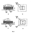
- a system 8 to form a relief pattern on a substrate 12 includes a stage 10 upon which substrate 12 is supported and a template 14, having a patterning surface 18 therein.
- substrate 12 may be coupled to a substrate chuck (not shown), the substrate chuck (not shown) being any chuck including, but not limited to, vacuum and electromagnetic.
- Template 14 and/or mold 16 may be formed from such materials including but not limited to, fused-silica, quartz, silicon, organic polymers, siloxane polymers, borosilicate glass, fluorocarbon polymers, metal, and hardened sapphire.
- patterning surface 18 comprises features defined by a plurality of spaced-apart recesses 17 and protrusions 19.
- patterning surface 18 may be substantially smooth and/or planar. Patterning surface 18 may define an original pattern that forms the basis of a pattern to be formed on substrate 12.
- Template 14 may be coupled to an imprint head 20 to facilitate movement of template 14, and therefore, mold 16.
- template 14 may be coupled to a template chuck (not shown), the template chuck (not shown) being any chuck including, but not limited to, vacuum and electromagnetic.
- a fluid dispense system 22 is coupled to be selectively placed in fluid communication with substrate 12 so as to deposit polymeric material 24 thereon.
- polymeric material 24 may be deposited using any known technique, e.g., drop dispense, spin-coating, dip coating, chemical vapor deposition (CVD), physical vapor deposition (PVD), and the like.
- polymeric material 24 may be positioned upon substrate 12 prior to establishing an environment between mold 16 and substrate 12, described further below, or in a further embodiment, fluid dispense system 22 may be positioned between substrate 12 and template 14.
- a source 26 of energy 28 is coupled to direct energy 28 along a path 30.
- Imprint head 20 and stage 10 are configured to arrange mold 16 and substrate 12, respectively, to be in superimposition and disposed in path 30. Either imprint head 20, stage 10, or both vary a distance between mold 16 and substrate 12 to define a desired volume therebetween that is filled by polymeric material 24.
- polymeric material 24 is disposed upon substrate 12 before the desired volume is defined between mold 16 and substrate 12. However, polymeric material 24 may fill the volume after the desired volume has been obtained.
- source 26 produces energy 28, e.g., broadband energy that causes polymeric material 24 to solidify and/or cross-link conforming to the shape of a surface 25 of substrate 12 and patterning surface 18, defining a patterned layer 50 on substrate 12.
- the broadband energy may comprise an actinic component including, but not limited to, ultraviolet wavelengths, thermal energy, electromagnetic energy, visible light and the like.
- the actinic component employed is known to one skilled in the art and typically depends on the material from which imprinting layer 12 is formed. Control of this process is regulated by a processor 32 that is in data communication with stage 10, imprint head 20, fluid dispense system 22, source 26, operating on a computer readable program stored in memory 34.
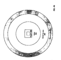
- a chamber concept to create and maintain a pressure in the vicinity of the template creates a leak proof volume around the active area of the template that can then be pressurized with gas or evacuated. Due to the template geometry, the etched back region around the active area conveniently provides such a volume, when the template is in contact with a wafer. Since the etched back region is about 5-15 ⁇ m higher than the active area, it also provides a very high flow resistance to any gas/ fluid.
- Figs. 2 a) - d) illustrate partial vacuum environments using a template 203-211 that has channels 213 or holes 204 for pneumatic flows. It is desirable to have a multiple source (e.g., holed 204) of the flow or a surrounding channel 213 in order to induce a uniform partial vacuum below the active area 202-212 of the template 205, 214. Vacuum-flow through the openings 204, 216 will pull away existing air or gas, which in the presence of a significant pressure drop due to the small but long gap, lowers the pressure between the active area 202, 212 and the substrate 201, 210.
- US 2005/0072755 Al describes a method of introducing a flow between the template 203, 211 and the substrate 201, 210.
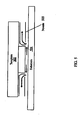
- the added extension parts can have an air bearing where it interfaces with the mating surface.
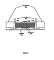
- Fig. 4 illustrates a cross-section view of a partial pressure imprinting tool that creates partial pressure between the substrate 402 and template 403.
- Vacuum preloaded air bearings can substantially seal the mini-environment 405 which can be filled with a suitable process gas (e.g., He) replacing air.
- the air bearing interface is positioned adjacent the plate 406. Channels (not shown) can cause an evacuation 408 from the environment 405, while pressurized gas 407 can be channeled through the air bearing ring 410 in a balance of the air bearing reference surface 406 and corresponding template stage 404.
- the upward air bearing can be lowered to provide an access for the wafer I/O end-effecter.
- Fig. 5 shows a system of nozzles that are utilized to create a partial He environment between the template 502 and the substrate 501.
Abstract
Description
- The invention pertains to a nanolithography imprinting system.
- Nano-fabrication involves the fabrication of very small structures, e.g., having features on the order of nanometers or smaller. One area in which nano-fabrication has had a sizeable impact is in the processing of integrated circuits. As the semiconductor processing industry continues to strive for larger production yields while increasing the circuits per unit area formed on a substrate, nano-fabrication becomes increasingly important. Nano-fabrication provides greater process control while allowing increased reduction of the minimum feature dimension of the structures formed. Other areas of development in which nano-fabrication has been employed include biotechnology, optical technology, mechanical systems and the like.
- An exemplary nano-fabrication technique is commonly referred to as imprint lithography. Exemplary imprint lithography processes are described in detail in numerous publications, such as
US 2004/0065976 A1 ,US 2004/0065252 A1 andUS-A-6,936,194 . - The fundamental imprint lithography technique disclosed in each of the aforementioned United States patent application publications and United States patent includes formation of a relief pattern in a polymerizable layer and transferring a pattern corresponding to the relief pattern into an underlying substrate. The substrate may be positioned upon a motion stage to obtain a desired position to facilitate patterning thereof. A template is employed spaced-apart from the substrate with a formable liquid present between the template and the substrate. The liquid is solidified to form a solidified layer that has a pattern recorded therein that is conforming to a shape of the surface of the template in contact with the liquid. The template is then separated from the solidified layer such that the template and the substrate are spaced-apart. The substrate and the solidified layer are then subjected to processes to transfer, into the substrate, a relief image that corresponds to the pattern in the solidified layer.
- There is a need for system for making imprint lithography more efficient and attractive.
- This is achieved by the system of the main claim.
- The imprint lithography is more efficient by creating a specific environment between a template and a substrate during a nanolithography imprinting process, in particular by partial vacuum environment imprinting.
- Preferred embodiments of the invention are characterized in the sub-claims.
- Preferred embodiments of the invention are now disclosed with reference to the drawings in which:
-
Fig. 1 is a simplified side view of a lithographic system having a template spaced-apart from a substrate; -
Fig. 2 illustrates a partial vacuum environment through a template: a) side view of a template with holes; b) top view of the template of a) with multiple holes, c) side view of a template with channel; d) top view of a template of c); -
Fig. 3 illustrates an additional add-on plate; -
Fig. 4 illustrates a partial vacuum environment using upward air bearing that acts as semi-sealing around the template; and -
Fig. 5 illustrates an alternative embodiment of the present invention. - Referring to
Fig. 1 , a system 8 to form a relief pattern on asubstrate 12 includes astage 10 upon whichsubstrate 12 is supported and atemplate 14, having apatterning surface 18 therein. In a further embodiment,substrate 12 may be coupled to a substrate chuck (not shown), the substrate chuck (not shown) being any chuck including, but not limited to, vacuum and electromagnetic. -
Template 14 and/ormold 16 may be formed from such materials including but not limited to, fused-silica, quartz, silicon, organic polymers, siloxane polymers, borosilicate glass, fluorocarbon polymers, metal, and hardened sapphire. As shown,patterning surface 18 comprises features defined by a plurality of spaced-apart recesses 17 andprotrusions 19. However, in a further embodiment, patterningsurface 18 may be substantially smooth and/or planar.Patterning surface 18 may define an original pattern that forms the basis of a pattern to be formed onsubstrate 12. -
Template 14 may be coupled to animprint head 20 to facilitate movement oftemplate 14, and therefore,mold 16. In a further embodiment,template 14 may be coupled to a template chuck (not shown), the template chuck (not shown) being any chuck including, but not limited to, vacuum and electromagnetic. A fluid dispensesystem 22 is coupled to be selectively placed in fluid communication withsubstrate 12 so as to depositpolymeric material 24 thereon. It should be understood thatpolymeric material 24 may be deposited using any known technique, e.g., drop dispense, spin-coating, dip coating, chemical vapor deposition (CVD), physical vapor deposition (PVD), and the like. Furthermore,polymeric material 24 may be positioned uponsubstrate 12 prior to establishing an environment betweenmold 16 andsubstrate 12, described further below, or in a further embodiment, fluid dispensesystem 22 may be positioned betweensubstrate 12 andtemplate 14. - A
source 26 ofenergy 28 is coupled todirect energy 28 along apath 30.Imprint head 20 andstage 10 are configured to arrangemold 16 andsubstrate 12, respectively, to be in superimposition and disposed inpath 30. Eitherimprint head 20,stage 10, or both vary a distance betweenmold 16 andsubstrate 12 to define a desired volume therebetween that is filled bypolymeric material 24. - Referring to
Fig. 1 ,polymeric material 24 is disposed uponsubstrate 12 before the desired volume is defined betweenmold 16 andsubstrate 12. However,polymeric material 24 may fill the volume after the desired volume has been obtained. After the desired volume is filled withpolymeric material 24,source 26 producesenergy 28, e.g., broadband energy that causespolymeric material 24 to solidify and/or cross-link conforming to the shape of a surface 25 ofsubstrate 12 andpatterning surface 18, defining a patterned layer 50 onsubstrate 12. - The broadband energy may comprise an actinic component including, but not limited to, ultraviolet wavelengths, thermal energy, electromagnetic energy, visible light and the like. The actinic component employed is known to one skilled in the art and typically depends on the material from which
imprinting layer 12 is formed. Control of this process is regulated by aprocessor 32 that is in data communication withstage 10,imprint head 20, fluid dispensesystem 22,source 26, operating on a computer readable program stored inmemory 34. - The following three capabilities are thought to assist in making imprint lithography more efficient and attractive:
- 1. Creation and maintenance of pure Helium or other process gas atmosphere such as CO2;
- 2. Partial or full vacuum imprinting (to reduce fill time, defects, and oxygen poisoning); and
- 3. Separation force reduction or elimination.
- A chamber concept to create and maintain a pressure in the vicinity of the template creates a leak proof volume around the active area of the template that can then be pressurized with gas or evacuated. Due to the template geometry, the etched back region around the active area conveniently provides such a volume, when the template is in contact with a wafer. Since the etched back region is about 5-15 µm higher than the active area, it also provides a very high flow resistance to any gas/ fluid.
-
Figs. 2 a) - d) illustrate partial vacuum environments using a template 203-211 that haschannels 213 orholes 204 for pneumatic flows. It is desirable to have a multiple source (e.g., holed 204) of the flow or a surroundingchannel 213 in order to induce a uniform partial vacuum below the active area 202-212 of thetemplate openings active area substrate US 2005/0072755 Al describes a method of introducing a flow between thetemplate substrate - Referring to
Fig. 3 , when thetemplate 302 cannot be drilled or processed for the channel, it is possible to addadditional plates 304 outside of thetemplate 302 so that thesmall gap 305 between this addedplate 304 and thetemplate 302 can generate a necessary pneumatic pressure drop between theactive area 306 and thesubstrate 301. In order to maintain the small gap in the range of 5-50 microns, the added extension parts can have an air bearing where it interfaces with the mating surface. -
Fig. 4 illustrates a cross-section view of a partial pressure imprinting tool that creates partial pressure between thesubstrate 402 andtemplate 403. Vacuum preloaded air bearings can substantially seal the mini-environment 405 which can be filled with a suitable process gas (e.g., He) replacing air. The air bearing interface is positioned adjacent the plate 406. Channels (not shown) can cause anevacuation 408 from theenvironment 405, whilepressurized gas 407 can be channeled through theair bearing ring 410 in a balance of the air bearing reference surface 406 andcorresponding template stage 404. Once the imprinting is completed for the wafer, the upward air bearing can be lowered to provide an access for the wafer I/O end-effecter. -
Fig. 5 shows a system of nozzles that are utilized to create a partial He environment between thetemplate 502 and thesubstrate 501. - The embodiments of the present invention described above are exemplary. The scope of the invention is determined with reference to the appended claims .
Claims (8)
- A system for creating a specific environment between a template and a substrate during a nanolithography imprinting process, comprising:a substrate (12; 201; 210; 301; 402; 501);a template (14; 203; 211; 302; 403; 502) positioned in close proximity to the substrate creating a volume of space between a nano-imprint mold (16) on the template and a corresponding location on the substrate (12; 201; 210; 301; 402; 501);anda means for creating a partial evacuation of gas in the volume of space between the nano-imprint mold (16) and the substrate (12; 201; 210; 301; 402; 501), characterized in that the system comprises:an air bearing around the template to seal or semi-seal the volume of space.
- The system as recited in claim 1, wherein the template further comprises a plurality of holes (204) positioned around the nano-imprint mold and passing through the template, the creating means utilizing the plurality of holes to create the partial evacuation of gas in the volume of space between the nano-imprint mold and the substrate.
- The system as recited in claim 1, wherein the template further comprises a channel (213) formed in the template around the nano-imprint mold, the channel coupled to the creating means.
- The system as recited in claim 1, wherein the creating means further comprises a body (304) positioned around the template (302) in a configuration that creates a gap (305) between sides of the template and sides of the body whereby air flow up through the gap evacuates gas from between the template (302) and the substrate (301).
- The system as recited in claim 1, wherein the substrate is coupled to a substrate chuck (401).
- The system as recited in claim 5, wherein the substrate chuck (401) comprises evacuation channels (408) for evacuating gas from the volume of space.
- The system as recited in claim 5, wherein template (403) has a template stage (404) with an air bearing reference surface (406), an air bearing ring (410) being positioned between the substrate chuck (401) and the air bearing surface (406) and creating an air bearing interface adjacent the air bearing surface (406).
- The system as recited in any one of the preceding claims, further comprising a polymerizable fluid (24) dispensed between the nano-imprint mold (16) and the substrate (12; 201; 210; 301; 402; 501).
Applications Claiming Priority (2)
| Application Number | Priority Date | Filing Date | Title |
|---|---|---|---|
| US78877906P | 2006-04-03 | 2006-04-03 | |
| PCT/US2007/008075 WO2007123805A2 (en) | 2006-04-03 | 2007-04-02 | Lithography imprinting system |
Publications (3)
| Publication Number | Publication Date |
|---|---|
| EP2001602A2 EP2001602A2 (en) | 2008-12-17 |
| EP2001602A4 EP2001602A4 (en) | 2009-04-01 |
| EP2001602B1 true EP2001602B1 (en) | 2011-06-22 |
Family
ID=38625508
Family Applications (1)
| Application Number | Title | Priority Date | Filing Date |
|---|---|---|---|
| EP07754579A Active EP2001602B1 (en) | 2006-04-03 | 2007-04-02 | Lithography imprinting system |
Country Status (8)
| Country | Link |
|---|---|
| US (1) | US7462028B2 (en) |
| EP (1) | EP2001602B1 (en) |
| JP (2) | JP4536148B2 (en) |
| KR (1) | KR20080114681A (en) |
| CN (1) | CN101405087A (en) |
| AT (1) | ATE513625T1 (en) |
| TW (1) | TWI432311B (en) |
| WO (1) | WO2007123805A2 (en) |
Families Citing this family (76)
| Publication number | Priority date | Publication date | Assignee | Title |
|---|---|---|---|---|
| US6119463A (en) | 1998-05-12 | 2000-09-19 | Amerigon | Thermoelectric heat exchanger |
| US7442336B2 (en) * | 2003-08-21 | 2008-10-28 | Molecular Imprints, Inc. | Capillary imprinting technique |
| US7077992B2 (en) * | 2002-07-11 | 2006-07-18 | Molecular Imprints, Inc. | Step and repeat imprint lithography processes |
| US7019819B2 (en) | 2002-11-13 | 2006-03-28 | Molecular Imprints, Inc. | Chucking system for modulating shapes of substrates |
| US8211214B2 (en) | 2003-10-02 | 2012-07-03 | Molecular Imprints, Inc. | Single phase fluid imprint lithography method |
| US20060062922A1 (en) | 2004-09-23 | 2006-03-23 | Molecular Imprints, Inc. | Polymerization technique to attenuate oxygen inhibition of solidification of liquids and composition therefor |
| US7587901B2 (en) | 2004-12-20 | 2009-09-15 | Amerigon Incorporated | Control system for thermal module in vehicle |
| US7611348B2 (en) * | 2005-04-19 | 2009-11-03 | Asml Netherlands B.V. | Imprint lithography |
| US7670530B2 (en) | 2006-01-20 | 2010-03-02 | Molecular Imprints, Inc. | Patterning substrates employing multiple chucks |
| WO2007067488A2 (en) | 2005-12-08 | 2007-06-14 | Molecular Imprints, Inc. | Method and system for double-sided patterning of substrates |
| EP1984208B1 (en) | 2006-01-30 | 2012-02-29 | Amerigon, Inc. | Cooling system for container in a vehicle |
| US8215946B2 (en) | 2006-05-18 | 2012-07-10 | Molecular Imprints, Inc. | Imprint lithography system and method |
| US8539624B2 (en) | 2006-05-31 | 2013-09-24 | Gentherm Incorporated | Structure based fluid distribution system |
| US20080087316A1 (en) | 2006-10-12 | 2008-04-17 | Masa Inaba | Thermoelectric device with internal sensor |
| ES2534460T3 (en) | 2006-10-13 | 2015-04-23 | Gentherm Incorporated | Air-conditioned bed |
| WO2008082650A1 (en) * | 2006-12-29 | 2008-07-10 | Molecular Imprints, Inc. | Imprint fluid control |
| KR101319325B1 (en) * | 2006-12-29 | 2013-10-16 | 엘지디스플레이 주식회사 | Method for Forming Pattern |
| US9105808B2 (en) | 2007-01-10 | 2015-08-11 | Gentherm Incorporated | Thermoelectric device |
| US20090014917A1 (en) * | 2007-07-10 | 2009-01-15 | Molecular Imprints, Inc. | Drop Pattern Generation for Imprint Lithography |
| US9105809B2 (en) | 2007-07-23 | 2015-08-11 | Gentherm Incorporated | Segmented thermoelectric device |
| WO2009036077A1 (en) | 2007-09-10 | 2009-03-19 | Amerigon, Inc. | Operational control schemes for ventilated seat or bed assemblies |
| US9125497B2 (en) | 2007-10-15 | 2015-09-08 | Gentherm Incorporated | Climate controlled bed assembly with intermediate layer |
| US8119052B2 (en) * | 2007-11-02 | 2012-02-21 | Molecular Imprints, Inc. | Drop pattern generation for imprint lithography |
| JP4840668B2 (en) * | 2007-11-30 | 2011-12-21 | 綜研化学株式会社 | Thermal imprint mold and method for producing optical element using the mold |
| US20090148619A1 (en) * | 2007-12-05 | 2009-06-11 | Molecular Imprints, Inc. | Controlling Thickness of Residual Layer |
| US20090196826A1 (en) * | 2007-12-18 | 2009-08-06 | Board Of Regents, The University Of Texas System | Compositions and methods of making non-spherical micro- and nano-particles |
| WO2009097572A1 (en) | 2008-02-01 | 2009-08-06 | Amerigon Incorporated | Condensation and humidity sensors for thermoelectric devices |
| US8361371B2 (en) * | 2008-02-08 | 2013-01-29 | Molecular Imprints, Inc. | Extrusion reduction in imprint lithography |
| JP5121549B2 (en) * | 2008-04-21 | 2013-01-16 | 株式会社東芝 | Nanoimprint method |
| US20100015270A1 (en) * | 2008-07-15 | 2010-01-21 | Molecular Imprints, Inc. | Inner cavity system for nano-imprint lithography |
| CN104523071A (en) | 2008-07-18 | 2015-04-22 | 金瑟姆股份公司 | Climate controlled bed assembly |
| US20100096764A1 (en) * | 2008-10-20 | 2010-04-22 | Molecular Imprints, Inc. | Gas Environment for Imprint Lithography |
| US8512797B2 (en) * | 2008-10-21 | 2013-08-20 | Molecular Imprints, Inc. | Drop pattern generation with edge weighting |
| US8586126B2 (en) | 2008-10-21 | 2013-11-19 | Molecular Imprints, Inc. | Robust optimization to generate drop patterns in imprint lithography which are tolerant of variations in drop volume and drop placement |
| TWI414418B (en) * | 2008-10-23 | 2013-11-11 | Molecular Imprints Inc | Imprint lithography system and method |
| US20100112220A1 (en) * | 2008-11-03 | 2010-05-06 | Molecular Imprints, Inc. | Dispense system set-up and characterization |
| WO2010088405A1 (en) | 2009-01-28 | 2010-08-05 | Amerigon Incorporated | Convective heater |
| KR20120001768A (en) | 2009-03-23 | 2012-01-04 | 인테벡, 인코포레이티드 | A process for optimization of island to trench ratio in patterned media |
| US8893329B2 (en) | 2009-05-06 | 2014-11-25 | Gentherm Incorporated | Control schemes and features for climate-controlled beds |
| JP5349595B2 (en) * | 2009-07-09 | 2013-11-20 | インハ インダストリー パートナーシップ インスティテュート | Microlens array manufacturing apparatus and microlens array manufacturing method |
| EP2287666B1 (en) | 2009-08-22 | 2012-06-27 | EV Group E. Thallner GmbH | Device for embossing substrates |
| US8332975B2 (en) | 2009-08-31 | 2012-12-18 | Gentherm Incorporated | Climate-controlled topper member for medical beds |
| JP5419634B2 (en) * | 2009-10-26 | 2014-02-19 | 株式会社東芝 | Pattern formation method |
| US20110140304A1 (en) * | 2009-12-10 | 2011-06-16 | Molecular Imprints, Inc. | Imprint lithography template |
| WO2011100050A2 (en) * | 2010-02-09 | 2011-08-18 | Molecular Imprints, Inc. | Process gas confinement for nano-imprinting |
| JP5491931B2 (en) * | 2010-03-30 | 2014-05-14 | 富士フイルム株式会社 | Nanoimprint method and mold manufacturing method |
| JP5822597B2 (en) * | 2010-10-01 | 2015-11-24 | キヤノン株式会社 | Imprint apparatus and article manufacturing method using the same |
| JP5930622B2 (en) | 2010-10-08 | 2016-06-08 | キヤノン株式会社 | Imprint apparatus and article manufacturing method |
| US9121414B2 (en) | 2010-11-05 | 2015-09-01 | Gentherm Incorporated | Low-profile blowers and methods |
| WO2012083578A1 (en) * | 2010-12-22 | 2012-06-28 | 青岛理工大学 | Device and method for nano-imprinting full wafer |
| JP5787691B2 (en) * | 2011-09-21 | 2015-09-30 | キヤノン株式会社 | Imprint apparatus and article manufacturing method using the same |
| US9685599B2 (en) | 2011-10-07 | 2017-06-20 | Gentherm Incorporated | Method and system for controlling an operation of a thermoelectric device |
| US9989267B2 (en) | 2012-02-10 | 2018-06-05 | Gentherm Incorporated | Moisture abatement in heating operation of climate controlled systems |
| KR101515180B1 (en) * | 2012-05-18 | 2015-04-24 | 주식회사 휴템 | Substrates bonding apparatus unsing fluid pressure and substrates bonding method |
| US20130337176A1 (en) * | 2012-06-19 | 2013-12-19 | Seagate Technology Llc | Nano-scale void reduction |
| WO2014008423A2 (en) | 2012-07-06 | 2014-01-09 | Gentherm Incorporated | Systems and methods for cooling inductive charging assemblies |
| US9662962B2 (en) | 2013-11-05 | 2017-05-30 | Gentherm Incorporated | Vehicle headliner assembly for zonal comfort |
| WO2015085150A1 (en) | 2013-12-05 | 2015-06-11 | Gentherm Incorporated | Systems and methods for climate controlled seats |
| JP6294679B2 (en) | 2014-01-21 | 2018-03-14 | キヤノン株式会社 | Imprint apparatus and article manufacturing method |
| KR102051617B1 (en) | 2014-02-14 | 2019-12-03 | 젠썸 인코포레이티드 | Conductive convective climate controlled seat |
| KR102449808B1 (en) | 2014-05-09 | 2022-09-29 | 젠썸 인코포레이티드 | Climate control assembly |
| JP6400090B2 (en) * | 2014-05-29 | 2018-10-03 | キヤノン株式会社 | Coating apparatus, imprint apparatus, and article manufacturing method |
| JP6361303B2 (en) * | 2014-06-13 | 2018-07-25 | 大日本印刷株式会社 | Imprint mold and imprint apparatus |
| CN107251247B (en) | 2014-11-14 | 2021-06-01 | 查尔斯·J·柯西 | Heating and cooling techniques |
| US11857004B2 (en) | 2014-11-14 | 2024-01-02 | Gentherm Incorporated | Heating and cooling technologies |
| US11639816B2 (en) | 2014-11-14 | 2023-05-02 | Gentherm Incorporated | Heating and cooling technologies including temperature regulating pad wrap and technologies with liquid system |
| JP6525567B2 (en) * | 2014-12-02 | 2019-06-05 | キヤノン株式会社 | Imprint apparatus and method of manufacturing article |
| CN104637843B (en) * | 2015-02-02 | 2017-12-05 | 京东方科技集团股份有限公司 | Sealed in unit and method for packing |
| WO2016128493A1 (en) * | 2015-02-13 | 2016-08-18 | Morphotonics Holding B.V. | Method for texturing discrete substrates ii |
| CN107364057A (en) * | 2017-07-10 | 2017-11-21 | 天津工业大学 | A kind of preparation method of different roughness template |
| JP6992331B2 (en) * | 2017-09-05 | 2022-01-13 | 大日本印刷株式会社 | Imprint mold |
| US10895806B2 (en) * | 2017-09-29 | 2021-01-19 | Canon Kabushiki Kaisha | Imprinting method and apparatus |
| JP7077754B2 (en) * | 2018-05-08 | 2022-05-31 | 大日本印刷株式会社 | Imprint mold substrate, imprint mold and their manufacturing method |
| US11075331B2 (en) | 2018-07-30 | 2021-07-27 | Gentherm Incorporated | Thermoelectric device having circuitry with structural rigidity |
| US11152557B2 (en) | 2019-02-20 | 2021-10-19 | Gentherm Incorporated | Thermoelectric module with integrated printed circuit board |
| US11590687B2 (en) | 2020-06-30 | 2023-02-28 | Canon Kabushiki Kaisha | Systems and methods for reducing pressure while shaping a film |
Family Cites Families (46)
| Publication number | Priority date | Publication date | Assignee | Title |
|---|---|---|---|---|
| US4279628A (en) | 1979-12-31 | 1981-07-21 | Energy Synergistics, Inc. | Apparatus for drying a natural gas stream |
| DE8007086U1 (en) | 1980-03-14 | 1982-03-18 | Multivac Sepp Haggenmüller KG, 8941 Wolfertschwenden | DEVICE FOR MOLDING CONTAINERS FROM A FILM |
| US4767584A (en) | 1985-04-03 | 1988-08-30 | Massachusetts Institute Of Technology | Process of and apparatus for producing design patterns in materials |
| DE3514022C1 (en) | 1985-04-18 | 1986-07-10 | Fa. Carl Freudenberg, 6940 Weinheim | Device for the mutual bonding of thermally softenable particles to a plastic body |
| US5108532A (en) * | 1988-02-02 | 1992-04-28 | Northrop Corporation | Method and apparatus for shaping, forming, consolidating and co-consolidating thermoplastic or thermosetting composite products |
| US5821175A (en) | 1988-07-08 | 1998-10-13 | Cauldron Limited Partnership | Removal of surface contaminants by irradiation using various methods to achieve desired inert gas flow over treated surface |
| JPH0292603A (en) * | 1988-09-30 | 1990-04-03 | Hoya Corp | Manufacture of data recording board with guide groove |
| US5545367A (en) | 1992-04-15 | 1996-08-13 | Soane Technologies, Inc. | Rapid prototype three dimensional stereolithography |
| FR2690375B1 (en) | 1992-04-22 | 1994-07-08 | Aerospatiale | HOT COMPACTION DEVICE FOR THE MANUFACTURE OF PARTS REQUIRING SIMULTANEOUS PRESSURE AND TEMPERATURE INCREASES. |
| US5997273A (en) | 1995-08-01 | 1999-12-07 | Laquer; Henry Louis | Differential pressure HIP forging in a controlled gaseous environment |
| US6482742B1 (en) * | 2000-07-18 | 2002-11-19 | Stephen Y. Chou | Fluid pressure imprint lithography |
| US5669303A (en) * | 1996-03-04 | 1997-09-23 | Motorola | Apparatus and method for stamping a surface |
| US6257866B1 (en) | 1996-06-18 | 2001-07-10 | Hy-Tech Forming Systems, Inc. | Apparatus for accurately forming plastic sheet |
| DE19819761C2 (en) | 1998-05-04 | 2000-05-31 | Jenoptik Jena Gmbh | Device for separating a shaped substrate from an embossing tool |
| US5997963A (en) | 1998-05-05 | 1999-12-07 | Ultratech Stepper, Inc. | Microchamber |
| US6099771A (en) | 1998-07-08 | 2000-08-08 | Lear Corporation | Vacuum compression method for forming molded thermoplastic floor mat having a "Class A" finish |
| US5947027A (en) * | 1998-09-08 | 1999-09-07 | Motorola, Inc. | Printing apparatus with inflatable means for advancing a substrate towards the stamping surface |
| JP3291488B2 (en) | 1999-05-27 | 2002-06-10 | 三洋電機株式会社 | Fluid removal method |
| EP1072954A3 (en) * | 1999-07-28 | 2002-05-22 | Lucent Technologies Inc. | Lithographic process for device fabrication |
| US6873087B1 (en) * | 1999-10-29 | 2005-03-29 | Board Of Regents, The University Of Texas System | High precision orientation alignment and gap control stages for imprint lithography processes |
| SE515607C2 (en) * | 1999-12-10 | 2001-09-10 | Obducat Ab | Device and method for fabrication of structures |
| DE10010001A1 (en) * | 2000-03-02 | 2001-09-06 | Celanese Ventures Gmbh | Membranes useful in fuel cells comprise a blend of sulfonated aryl polymer, aminated or nitrated polyether(ether)sulfone and plasticizer |
| JP2001358056A (en) | 2000-06-15 | 2001-12-26 | Canon Inc | Exposure apparatus |
| US7322287B2 (en) * | 2000-07-18 | 2008-01-29 | Nanonex Corporation | Apparatus for fluid pressure imprint lithography |
| AU2001280980A1 (en) * | 2000-08-01 | 2002-02-13 | Board Of Regents, The University Of Texas System | Methods for high-precision gap and orientation sensing between a transparent template and substrate for imprint lithography |
| EP1352295B1 (en) * | 2000-10-12 | 2015-12-23 | Board of Regents, The University of Texas System | Template for room temperature, low pressure micro- and nano-imprint lithography |
| JP2002208563A (en) | 2001-01-09 | 2002-07-26 | Ebara Corp | Equipment and method for processing workpiece |
| JP2003109915A (en) * | 2001-09-28 | 2003-04-11 | National Institute Of Advanced Industrial & Technology | Method and device for performing in-print lithography in releasable atmosphere |
| US20030071016A1 (en) * | 2001-10-11 | 2003-04-17 | Wu-Sheng Shih | Patterned structure reproduction using nonsticking mold |
| US6764386B2 (en) | 2002-01-11 | 2004-07-20 | Applied Materials, Inc. | Air bearing-sealed micro-processing chamber |
| US7019819B2 (en) | 2002-11-13 | 2006-03-28 | Molecular Imprints, Inc. | Chucking system for modulating shapes of substrates |
| US6932934B2 (en) * | 2002-07-11 | 2005-08-23 | Molecular Imprints, Inc. | Formation of discontinuous films during an imprint lithography process |
| MY164487A (en) * | 2002-07-11 | 2017-12-29 | Molecular Imprints Inc | Step and repeat imprint lithography processes |
| KR20050026088A (en) * | 2002-08-01 | 2005-03-14 | 몰레큘러 임프린츠 인코퍼레이티드 | Scatterometry alignment for imprint lithography |
| JP2004071934A (en) * | 2002-08-08 | 2004-03-04 | Kanegafuchi Chem Ind Co Ltd | Method for manufacturing fine pattern and transfer material |
| JP3700001B2 (en) * | 2002-09-10 | 2005-09-28 | 独立行政法人産業技術総合研究所 | Imprint method and apparatus |
| US20040132301A1 (en) * | 2002-09-12 | 2004-07-08 | Harper Bruce M. | Indirect fluid pressure imprinting |
| US6986815B2 (en) | 2003-01-08 | 2006-01-17 | General Electric Company | Flow system flush process |
| US6951173B1 (en) * | 2003-05-14 | 2005-10-04 | Molecular Imprints, Inc. | Assembly and method for transferring imprint lithography templates |
| JP2005045168A (en) * | 2003-07-25 | 2005-02-17 | Tokyo Electron Ltd | In-print method and in-print device |
| JP4313109B2 (en) * | 2003-08-01 | 2009-08-12 | 明昌機工株式会社 | High precision press machine |
| JP2005101201A (en) | 2003-09-24 | 2005-04-14 | Canon Inc | Nano-imprint system |
| US7090716B2 (en) | 2003-10-02 | 2006-08-15 | Molecular Imprints, Inc. | Single phase fluid imprint lithography method |
| US7500603B2 (en) * | 2004-02-19 | 2009-03-10 | Capital One Financial Corporation | Data card |
| KR100558754B1 (en) * | 2004-02-24 | 2006-03-10 | 한국기계연구원 | Uv nanoimprint lithography process and apparatus for performing the same |
| US7316554B2 (en) | 2005-09-21 | 2008-01-08 | Molecular Imprints, Inc. | System to control an atmosphere between a body and a substrate |
-
2007
- 2007-04-02 AT AT07754579T patent/ATE513625T1/en not_active IP Right Cessation
- 2007-04-02 CN CNA2007800099833A patent/CN101405087A/en active Pending
- 2007-04-02 EP EP07754579A patent/EP2001602B1/en active Active
- 2007-04-02 KR KR1020087017591A patent/KR20080114681A/en not_active Application Discontinuation
- 2007-04-02 WO PCT/US2007/008075 patent/WO2007123805A2/en active Application Filing
- 2007-04-02 JP JP2009504231A patent/JP4536148B2/en active Active
- 2007-04-02 US US11/695,263 patent/US7462028B2/en active Active
- 2007-04-03 TW TW096111836A patent/TWI432311B/en active
-
2010
- 2010-03-19 JP JP2010063842A patent/JP4917159B2/en active Active
Also Published As
| Publication number | Publication date |
|---|---|
| TWI432311B (en) | 2014-04-01 |
| JP4917159B2 (en) | 2012-04-18 |
| EP2001602A4 (en) | 2009-04-01 |
| JP2009532245A (en) | 2009-09-10 |
| WO2007123805A3 (en) | 2007-12-27 |
| TW200744830A (en) | 2007-12-16 |
| JP2010179655A (en) | 2010-08-19 |
| EP2001602A2 (en) | 2008-12-17 |
| JP4536148B2 (en) | 2010-09-01 |
| US7462028B2 (en) | 2008-12-09 |
| CN101405087A (en) | 2009-04-08 |
| WO2007123805A2 (en) | 2007-11-01 |
| KR20080114681A (en) | 2008-12-31 |
| US20070275114A1 (en) | 2007-11-29 |
| ATE513625T1 (en) | 2011-07-15 |
Similar Documents
| Publication | Publication Date | Title |
|---|---|---|
| EP2001602B1 (en) | Lithography imprinting system | |
| US9227361B2 (en) | Imprint lithography template | |
| US7636999B2 (en) | Method of retaining a substrate to a wafer chuck | |
| US7798801B2 (en) | Chucking system for nano-manufacturing | |
| US7931846B2 (en) | Method to control an atmosphere between a body and a substrate | |
| JP5198282B2 (en) | Method for exhausting a gas located between a substrate and a mold | |
| US20070114686A1 (en) | Method for expelling gas positioned between a substrate and a mold | |
| US20050072755A1 (en) | Single phase fluid imprint lithography method | |
| EP2016613A2 (en) | Template having a varying thickness | |
| US20100015270A1 (en) | Inner cavity system for nano-imprint lithography | |
| US20110001954A1 (en) | Chucking system with recessed support feature | |
| US20110193251A1 (en) | Process Gas Confinement for Nano-Imprinting | |
| WO2006083520A2 (en) | Method of separating a mold from a solidified layer disposed on a substrate |
Legal Events
| Date | Code | Title | Description |
|---|---|---|---|
| PUAI | Public reference made under article 153(3) epc to a published international application that has entered the european phase |
Free format text: ORIGINAL CODE: 0009012 |
|
| 17P | Request for examination filed |
Effective date: 20080814 |
|
| AK | Designated contracting states |
Kind code of ref document: A2 Designated state(s): AT BE BG CH CY CZ DE DK EE ES FI FR GB GR HU IE IS IT LI LT LU LV MC MT NL PL PT RO SE SI SK TR |
|
| A4 | Supplementary search report drawn up and despatched |
Effective date: 20090303 |
|
| RIC1 | Information provided on ipc code assigned before grant |
Ipc: B05D 5/00 20060101AFI20080715BHEP Ipc: G03F 7/00 20060101ALI20090225BHEP |
|
| RIN1 | Information on inventor provided before grant (corrected) |
Inventor name: CHERALA, ANSHUMAN Inventor name: LAD, PANKAJ, B. Inventor name: CHOI, BYUNG-JIN Inventor name: MCMACKIN, IAN, M. |
|
| RIN1 | Information on inventor provided before grant (corrected) |
Inventor name: CHERALA, ANSHUMAN Inventor name: CHOI, BYUNG-JIN Inventor name: MCMACKIN, IAN, M. Inventor name: LAD, PANKAJ, B. |
|
| 17Q | First examination report despatched |
Effective date: 20090730 |
|
| GRAP | Despatch of communication of intention to grant a patent |
Free format text: ORIGINAL CODE: EPIDOSNIGR1 |
|
| GRAS | Grant fee paid |
Free format text: ORIGINAL CODE: EPIDOSNIGR3 |
|
| GRAA | (expected) grant |
Free format text: ORIGINAL CODE: 0009210 |
|
| AK | Designated contracting states |
Kind code of ref document: B1 Designated state(s): AT BE BG CH CY CZ DE DK EE ES FI FR GB GR HU IE IS IT LI LT LU LV MC MT NL PL PT RO SE SI SK TR |
|
| REG | Reference to a national code |
Ref country code: GB Ref legal event code: FG4D |
|
| REG | Reference to a national code |
Ref country code: CH Ref legal event code: EP |
|
| REG | Reference to a national code |
Ref country code: IE Ref legal event code: FG4D |
|
| REG | Reference to a national code |
Ref country code: DE Ref legal event code: R096 Ref document number: 602007015391 Country of ref document: DE Effective date: 20110811 |
|
| REG | Reference to a national code |
Ref country code: NL Ref legal event code: T3 |
|
| PG25 | Lapsed in a contracting state [announced via postgrant information from national office to epo] |
Ref country code: SE Free format text: LAPSE BECAUSE OF FAILURE TO SUBMIT A TRANSLATION OF THE DESCRIPTION OR TO PAY THE FEE WITHIN THE PRESCRIBED TIME-LIMIT Effective date: 20110622 Ref country code: LT Free format text: LAPSE BECAUSE OF FAILURE TO SUBMIT A TRANSLATION OF THE DESCRIPTION OR TO PAY THE FEE WITHIN THE PRESCRIBED TIME-LIMIT Effective date: 20110622 |
|
| PG25 | Lapsed in a contracting state [announced via postgrant information from national office to epo] |
Ref country code: GR Free format text: LAPSE BECAUSE OF FAILURE TO SUBMIT A TRANSLATION OF THE DESCRIPTION OR TO PAY THE FEE WITHIN THE PRESCRIBED TIME-LIMIT Effective date: 20110923 Ref country code: SI Free format text: LAPSE BECAUSE OF FAILURE TO SUBMIT A TRANSLATION OF THE DESCRIPTION OR TO PAY THE FEE WITHIN THE PRESCRIBED TIME-LIMIT Effective date: 20110622 Ref country code: AT Free format text: LAPSE BECAUSE OF FAILURE TO SUBMIT A TRANSLATION OF THE DESCRIPTION OR TO PAY THE FEE WITHIN THE PRESCRIBED TIME-LIMIT Effective date: 20110622 Ref country code: CY Free format text: LAPSE BECAUSE OF FAILURE TO SUBMIT A TRANSLATION OF THE DESCRIPTION OR TO PAY THE FEE WITHIN THE PRESCRIBED TIME-LIMIT Effective date: 20110622 Ref country code: FI Free format text: LAPSE BECAUSE OF FAILURE TO SUBMIT A TRANSLATION OF THE DESCRIPTION OR TO PAY THE FEE WITHIN THE PRESCRIBED TIME-LIMIT Effective date: 20110622 Ref country code: LV Free format text: LAPSE BECAUSE OF FAILURE TO SUBMIT A TRANSLATION OF THE DESCRIPTION OR TO PAY THE FEE WITHIN THE PRESCRIBED TIME-LIMIT Effective date: 20110622 |
|
| PG25 | Lapsed in a contracting state [announced via postgrant information from national office to epo] |
Ref country code: BE Free format text: LAPSE BECAUSE OF FAILURE TO SUBMIT A TRANSLATION OF THE DESCRIPTION OR TO PAY THE FEE WITHIN THE PRESCRIBED TIME-LIMIT Effective date: 20110622 |
|
| PG25 | Lapsed in a contracting state [announced via postgrant information from national office to epo] |
Ref country code: EE Free format text: LAPSE BECAUSE OF FAILURE TO SUBMIT A TRANSLATION OF THE DESCRIPTION OR TO PAY THE FEE WITHIN THE PRESCRIBED TIME-LIMIT Effective date: 20110622 Ref country code: IS Free format text: LAPSE BECAUSE OF FAILURE TO SUBMIT A TRANSLATION OF THE DESCRIPTION OR TO PAY THE FEE WITHIN THE PRESCRIBED TIME-LIMIT Effective date: 20111022 Ref country code: CZ Free format text: LAPSE BECAUSE OF FAILURE TO SUBMIT A TRANSLATION OF THE DESCRIPTION OR TO PAY THE FEE WITHIN THE PRESCRIBED TIME-LIMIT Effective date: 20110622 Ref country code: PT Free format text: LAPSE BECAUSE OF FAILURE TO SUBMIT A TRANSLATION OF THE DESCRIPTION OR TO PAY THE FEE WITHIN THE PRESCRIBED TIME-LIMIT Effective date: 20111024 |
|
| PG25 | Lapsed in a contracting state [announced via postgrant information from national office to epo] |
Ref country code: SK Free format text: LAPSE BECAUSE OF FAILURE TO SUBMIT A TRANSLATION OF THE DESCRIPTION OR TO PAY THE FEE WITHIN THE PRESCRIBED TIME-LIMIT Effective date: 20110622 Ref country code: RO Free format text: LAPSE BECAUSE OF FAILURE TO SUBMIT A TRANSLATION OF THE DESCRIPTION OR TO PAY THE FEE WITHIN THE PRESCRIBED TIME-LIMIT Effective date: 20110622 Ref country code: PL Free format text: LAPSE BECAUSE OF FAILURE TO SUBMIT A TRANSLATION OF THE DESCRIPTION OR TO PAY THE FEE WITHIN THE PRESCRIBED TIME-LIMIT Effective date: 20110622 |
|
| PLBE | No opposition filed within time limit |
Free format text: ORIGINAL CODE: 0009261 |
|
| STAA | Information on the status of an ep patent application or granted ep patent |
Free format text: STATUS: NO OPPOSITION FILED WITHIN TIME LIMIT |
|
| 26N | No opposition filed |
Effective date: 20120323 |
|
| PG25 | Lapsed in a contracting state [announced via postgrant information from national office to epo] |
Ref country code: IT Free format text: LAPSE BECAUSE OF FAILURE TO SUBMIT A TRANSLATION OF THE DESCRIPTION OR TO PAY THE FEE WITHIN THE PRESCRIBED TIME-LIMIT Effective date: 20110622 |
|
| PG25 | Lapsed in a contracting state [announced via postgrant information from national office to epo] |
Ref country code: DK Free format text: LAPSE BECAUSE OF FAILURE TO SUBMIT A TRANSLATION OF THE DESCRIPTION OR TO PAY THE FEE WITHIN THE PRESCRIBED TIME-LIMIT Effective date: 20110622 |
|
| REG | Reference to a national code |
Ref country code: DE Ref legal event code: R097 Ref document number: 602007015391 Country of ref document: DE Effective date: 20120323 |
|
| PG25 | Lapsed in a contracting state [announced via postgrant information from national office to epo] |
Ref country code: MC Free format text: LAPSE BECAUSE OF NON-PAYMENT OF DUE FEES Effective date: 20120430 |
|
| REG | Reference to a national code |
Ref country code: CH Ref legal event code: PL |
|
| GBPC | Gb: european patent ceased through non-payment of renewal fee |
Effective date: 20120402 |
|
| REG | Reference to a national code |
Ref country code: IE Ref legal event code: MM4A |
|
| REG | Reference to a national code |
Ref country code: FR Ref legal event code: ST Effective date: 20121228 |
|
| PG25 | Lapsed in a contracting state [announced via postgrant information from national office to epo] |
Ref country code: IE Free format text: LAPSE BECAUSE OF NON-PAYMENT OF DUE FEES Effective date: 20120402 Ref country code: GB Free format text: LAPSE BECAUSE OF NON-PAYMENT OF DUE FEES Effective date: 20120402 Ref country code: LI Free format text: LAPSE BECAUSE OF NON-PAYMENT OF DUE FEES Effective date: 20120430 Ref country code: CH Free format text: LAPSE BECAUSE OF NON-PAYMENT OF DUE FEES Effective date: 20120430 |
|
| PG25 | Lapsed in a contracting state [announced via postgrant information from national office to epo] |
Ref country code: FR Free format text: LAPSE BECAUSE OF NON-PAYMENT OF DUE FEES Effective date: 20120430 |
|
| PG25 | Lapsed in a contracting state [announced via postgrant information from national office to epo] |
Ref country code: ES Free format text: LAPSE BECAUSE OF FAILURE TO SUBMIT A TRANSLATION OF THE DESCRIPTION OR TO PAY THE FEE WITHIN THE PRESCRIBED TIME-LIMIT Effective date: 20111003 |
|
| PG25 | Lapsed in a contracting state [announced via postgrant information from national office to epo] |
Ref country code: BG Free format text: LAPSE BECAUSE OF FAILURE TO SUBMIT A TRANSLATION OF THE DESCRIPTION OR TO PAY THE FEE WITHIN THE PRESCRIBED TIME-LIMIT Effective date: 20110922 |
|
| PG25 | Lapsed in a contracting state [announced via postgrant information from national office to epo] |
Ref country code: MT Free format text: LAPSE BECAUSE OF FAILURE TO SUBMIT A TRANSLATION OF THE DESCRIPTION OR TO PAY THE FEE WITHIN THE PRESCRIBED TIME-LIMIT Effective date: 20110622 |
|
| PG25 | Lapsed in a contracting state [announced via postgrant information from national office to epo] |
Ref country code: TR Free format text: LAPSE BECAUSE OF FAILURE TO SUBMIT A TRANSLATION OF THE DESCRIPTION OR TO PAY THE FEE WITHIN THE PRESCRIBED TIME-LIMIT Effective date: 20110622 |
|
| PG25 | Lapsed in a contracting state [announced via postgrant information from national office to epo] |
Ref country code: LU Free format text: LAPSE BECAUSE OF NON-PAYMENT OF DUE FEES Effective date: 20120402 |
|
| PG25 | Lapsed in a contracting state [announced via postgrant information from national office to epo] |
Ref country code: HU Free format text: LAPSE BECAUSE OF FAILURE TO SUBMIT A TRANSLATION OF THE DESCRIPTION OR TO PAY THE FEE WITHIN THE PRESCRIBED TIME-LIMIT Effective date: 20070402 |
|
| PGFP | Annual fee paid to national office [announced via postgrant information from national office to epo] |
Ref country code: DE Payment date: 20230307 Year of fee payment: 17 |
|
| PGFP | Annual fee paid to national office [announced via postgrant information from national office to epo] |
Ref country code: NL Payment date: 20240320 Year of fee payment: 18 |