EP1994635B1 - Supply circuit and device comprising a supply circuit - Google Patents
Supply circuit and device comprising a supply circuit Download PDFInfo
- Publication number
- EP1994635B1 EP1994635B1 EP07735026A EP07735026A EP1994635B1 EP 1994635 B1 EP1994635 B1 EP 1994635B1 EP 07735026 A EP07735026 A EP 07735026A EP 07735026 A EP07735026 A EP 07735026A EP 1994635 B1 EP1994635 B1 EP 1994635B1
- Authority
- EP
- European Patent Office
- Prior art keywords
- signal
- circuit
- supply circuit
- output
- amplitude
- Prior art date
- Legal status (The legal status is an assumption and is not a legal conclusion. Google has not performed a legal analysis and makes no representation as to the accuracy of the status listed.)
- Not-in-force
Links
Images


Classifications
-
- H—ELECTRICITY
- H02—GENERATION; CONVERSION OR DISTRIBUTION OF ELECTRIC POWER
- H02M—APPARATUS FOR CONVERSION BETWEEN AC AND AC, BETWEEN AC AND DC, OR BETWEEN DC AND DC, AND FOR USE WITH MAINS OR SIMILAR POWER SUPPLY SYSTEMS; CONVERSION OF DC OR AC INPUT POWER INTO SURGE OUTPUT POWER; CONTROL OR REGULATION THEREOF
- H02M3/00—Conversion of dc power input into dc power output
- H02M3/22—Conversion of dc power input into dc power output with intermediate conversion into ac
- H02M3/24—Conversion of dc power input into dc power output with intermediate conversion into ac by static converters
- H02M3/28—Conversion of dc power input into dc power output with intermediate conversion into ac by static converters using discharge tubes with control electrode or semiconductor devices with control electrode to produce the intermediate ac
- H02M3/325—Conversion of dc power input into dc power output with intermediate conversion into ac by static converters using discharge tubes with control electrode or semiconductor devices with control electrode to produce the intermediate ac using devices of a triode or a transistor type requiring continuous application of a control signal
- H02M3/335—Conversion of dc power input into dc power output with intermediate conversion into ac by static converters using discharge tubes with control electrode or semiconductor devices with control electrode to produce the intermediate ac using devices of a triode or a transistor type requiring continuous application of a control signal using semiconductor devices only
- H02M3/337—Conversion of dc power input into dc power output with intermediate conversion into ac by static converters using discharge tubes with control electrode or semiconductor devices with control electrode to produce the intermediate ac using devices of a triode or a transistor type requiring continuous application of a control signal using semiconductor devices only in push-pull configuration
- H02M3/3376—Conversion of dc power input into dc power output with intermediate conversion into ac by static converters using discharge tubes with control electrode or semiconductor devices with control electrode to produce the intermediate ac using devices of a triode or a transistor type requiring continuous application of a control signal using semiconductor devices only in push-pull configuration with automatic control of output voltage or current
-
- H—ELECTRICITY
- H05—ELECTRIC TECHNIQUES NOT OTHERWISE PROVIDED FOR
- H05B—ELECTRIC HEATING; ELECTRIC LIGHT SOURCES NOT OTHERWISE PROVIDED FOR; CIRCUIT ARRANGEMENTS FOR ELECTRIC LIGHT SOURCES, IN GENERAL
- H05B45/00—Circuit arrangements for operating light-emitting diodes [LED]
- H05B45/30—Driver circuits
- H05B45/37—Converter circuits
- H05B45/3725—Switched mode power supply [SMPS]
- H05B45/382—Switched mode power supply [SMPS] with galvanic isolation between input and output
-
- H—ELECTRICITY
- H05—ELECTRIC TECHNIQUES NOT OTHERWISE PROVIDED FOR
- H05B—ELECTRIC HEATING; ELECTRIC LIGHT SOURCES NOT OTHERWISE PROVIDED FOR; CIRCUIT ARRANGEMENTS FOR ELECTRIC LIGHT SOURCES, IN GENERAL
- H05B45/00—Circuit arrangements for operating light-emitting diodes [LED]
- H05B45/30—Driver circuits
- H05B45/37—Converter circuits
- H05B45/3725—Switched mode power supply [SMPS]
- H05B45/39—Circuits containing inverter bridges
-
- Y—GENERAL TAGGING OF NEW TECHNOLOGICAL DEVELOPMENTS; GENERAL TAGGING OF CROSS-SECTIONAL TECHNOLOGIES SPANNING OVER SEVERAL SECTIONS OF THE IPC; TECHNICAL SUBJECTS COVERED BY FORMER USPC CROSS-REFERENCE ART COLLECTIONS [XRACs] AND DIGESTS
- Y02—TECHNOLOGIES OR APPLICATIONS FOR MITIGATION OR ADAPTATION AGAINST CLIMATE CHANGE
- Y02B—CLIMATE CHANGE MITIGATION TECHNOLOGIES RELATED TO BUILDINGS, e.g. HOUSING, HOUSE APPLIANCES OR RELATED END-USER APPLICATIONS
- Y02B20/00—Energy efficient lighting technologies, e.g. halogen lamps or gas discharge lamps
- Y02B20/30—Semiconductor lamps, e.g. solid state lamps [SSL] light emitting diodes [LED] or organic LED [OLED]
-
- Y—GENERAL TAGGING OF NEW TECHNOLOGICAL DEVELOPMENTS; GENERAL TAGGING OF CROSS-SECTIONAL TECHNOLOGIES SPANNING OVER SEVERAL SECTIONS OF THE IPC; TECHNICAL SUBJECTS COVERED BY FORMER USPC CROSS-REFERENCE ART COLLECTIONS [XRACs] AND DIGESTS
- Y02—TECHNOLOGIES OR APPLICATIONS FOR MITIGATION OR ADAPTATION AGAINST CLIMATE CHANGE
- Y02B—CLIMATE CHANGE MITIGATION TECHNOLOGIES RELATED TO BUILDINGS, e.g. HOUSING, HOUSE APPLIANCES OR RELATED END-USER APPLICATIONS
- Y02B70/00—Technologies for an efficient end-user side electric power management and consumption
- Y02B70/10—Technologies improving the efficiency by using switched-mode power supplies [SMPS], i.e. efficient power electronics conversion e.g. power factor correction or reduction of losses in power supplies or efficient standby modes
Definitions
- the invention relates to a supply circuit for supplying an output signal to a load, which supply circuit comprises
- the invention also relates to a device comprising a supply circuit.
- Examples of such a supply circuit are switched mode power supplies, without excluding other supply circuits.
- Examples of such a load are one light emitting diode and two or more serial light emitting diodes and two or more parallel light emitting diodes, without excluding other loads.
- a prior art supply circuit is known from US 6,853,150 B2 , which discloses a supply circuit comprising a transistor circuit with two transistors in a half bridge configuration and comprising an impedance circuit with an inductor and capacitors each coupled to light emitting diodes.
- the prior art supply circuit is disadvantageous, inter alia, in that a fluctuation in an input signal and/or a fluctuation in a voltage drop across the light emitting diodes may result in a fluctuation in an output signal, which may result in a fluctuation in a brightness of a light emitting diode.
- EP 0 317 698 discloses a neon tube lighting device with a transistor, a leakage transformer and a generator.
- US 2004 / 0183380 discloses a switching constant-current power supply system.
- US 2005 / 0281061 discloses a resonance converter with voltage regulation.
- US 6,420,858 discloses a DC-to-DC converter circuit having a power saving mode.
- Further objects of the invention are, inter alia, to provide a device comprising a supply circuit that supplies a relatively constant output signal to a load.
- the supply circuit for supplying an output signal to a load is defined according to claim 1.
- the supply circuit supplies a relatively constant output signal to a load.
- the input signal for example comprises an input voltage signal, without excluding other input signals
- the output signal for example comprises an output current signal, without excluding other output signals.
- the supply circuit according to the invention further reduces a dependency between for example an output voltage signal and for example an output current signal.
- the third circuit comprises an input for receiving the input signal and comprising an output for supplying the control signal in dependence of the input signal and independently from the output signal, to advantageously avoid a use of a disadvantageous feedback loop from the load (secondary side) to the first circuit (primary side).
- the control signal is supplied in dependence of a primary side signal and independently from a secondary side signal.
- the reference signal for example comprises a reference current signal, without excluding other reference signals.
- the third circuit comprises a control loop.
- the addition of the inversion of the converter output signal and the reference signal of course corresponds with a subtraction of the converter output signal from the reference signal.
- the multiplier output signal for example comprises a multiplier output voltage signal
- the low pass filter output signal for example comprises a low pass filter output voltage signal before entering the converter and for example comprises a low pass filter output current signal after having left the converter
- the adder output signal for example comprises an adder output current signal, without excluding other signals.
- An embodiment of the supply circuit according to the invention is defined by the pulse signal comprising first pulses having a first amplitude and comprising second pulses having a second amplitude different from the first amplitude and comprising levels having a third amplitude different from the first and second amplitudes.
- This embodiment advantageously introduces a pulse signal with three different amplitudes that increase a number of controlling options.
- the supply circuit according to the invention is defined by the first amplitude being a positive amplitude, the second amplitude being a negative amplitude, and the third amplitude being a substantially zero amplitude.
- This embodiment advantageously introduces a symmetrical pulse signal.
- the supply circuit according to the invention is defined by the first circuit comprising a first transistor having a first main electrode coupled to a first reference terminal and having a second main electrode coupled to a first input of the second circuit and comprising a second transistor having a first main electrode coupled to the second main electrode of the first transistor and having a second main electrode coupled to a second reference terminal and comprising a third transistor having a first main electrode coupled to the first reference terminal and having a second main electrode coupled to a second input of the second circuit and comprising a fourth transistor having a first main electrode coupled to the second main electrode of the third transistor and having a second main electrode coupled to the second reference terminal.
- This embodiment advantageously introduces a first circuit comprising four transistors in a full bridge configuration (H bridge).
- the supply circuit according to the invention is defined by the first circuit comprising logical circuitry for receiving the control signal and comprising outputs coupled to control electrodes of the transistors for bringing the first and fourth transistors in a conducting state to create the first pulses and for bringing the second and third transistors in a conducting state to create the second pulses and for bringing either the first and third or the second and fourth transistors in a conducting state to create the levels.
- This embodiment advantageously introduces logical circuitry into the first circuit for coupling the first and third circuits to each other.
- An embodiment of the supply circuit according to the invention is defined by the pulse signal comprising first pulses having a first amplitude and comprising second pulses having a second amplitude different from the first amplitude.
- This embodiment advantageously introduces a pulse signal with only two different amplitudes.
- the supply circuit according to the invention is defined by the first amplitude being a positive amplitude and the second amplitude being a negative amplitude.
- This embodiment advantageously introduces a symmetrical pulse signal.
- the supply circuit according to the invention is defined by the first circuit comprising the four transistor topology described above, which four transistors are operated in such a way that now only a pulse signal with two different amplitudes is introduced.
- This embodiment advantageously introduces a first circuit comprising four transistors in a full bridge configuration (H bridge) that now introduce a pulse signal with only two amplitudes.
- An embodiment of the supply circuit according to the invention is defined by the pulse signal comprising third pulses having a fourth amplitude and comprising a level having a fifth amplitude.
- This embodiment advantageously introduces a pulse signal with only two different amplitudes, one of these amplitudes being realized by a pulse and the other one of these amplitudes being realized by a level.
- the supply circuit according to the invention is defined by the fourth amplitude being a positive amplitude and the fifth amplitude being a substantially zero amplitude.
- This embodiment advantageously introduces an asymmetrical pulse signal.
- the supply circuit according to the invention is defined by the first circuit comprising a first transistor having a first main electrode coupled to a first reference terminal and having a second main electrode coupled to a first input of the second circuit and comprising a second transistor having a first main electrode coupled to the second main electrode of the first transistor and having a second main electrode coupled to a second reference terminal, which second reference terminal is further coupled to a second input of the second circuit.
- This embodiment advantageously introduces a first circuit comprising two transistors in a half bridge configuration.
- the supply circuit according to the invention is defined by the first circuit comprising logical circuitry for receiving the control signal and comprising outputs coupled to control electrodes of the transistors for bringing the first transistor in a conducting state to create the third pulses and for bringing the second transistor in a conducting state to create the levels.
- This embodiment advantageously introduces logical circuitry into the first circuit for coupling the first and third circuits to each other.
- the supply circuit according to the invention is defined by the first circuit comprising a half bridge, and the third circuit being arranged to drive the half bridge at Ts ⁇ 4*tau, where tau is half a resonance period of the resonance circuit and Ts is a switching period.
- An embodiment of the supply circuit according to the invention is defined by the resonance circuit comprising a transformer and a capacitor coupled serially to a primary side of the transformer or to a secondary side of the transformer.
- This embodiment advantageously introduces the transformer for providing galvanic isolation.
- the second circuit may further comprise a rectifying circuit comprising one or more diodes coupled to a secondary side of the transformer.
- This embodiment advantageously further introduces the capacitor for in combination with the leakage inductance of the transformer (and/or with a separate inductor) creating a resonant circuit.
- An embodiment of the supply circuit according to the invention is defined by the resonance circuit comprising an inductor and a capacitor coupled serially to a primary side of the inductor or to a secondary side of the inductor.
- This embodiment advantageously introduces the inductor.
- Such an inductor is more low cost than a transformer.
- the second circuit may further comprise a rectifying circuit comprising one or more diodes coupled to a secondary side of the inductor.
- This embodiment advantageously further introduces the capacitor for in combination with the inductor creating a resonant circuit.
- An embodiment of the supply circuit according to the invention is defined by the load comprising one or more light emitting diodes.
- An embodiment of the supply circuit according to the invention is defined by comprising one or more input diodes for rectifying an AC signal, the input signal comprising a rectified AC signal.
- the AC signal for example comprises an AC voltage signal, without excluding other AC signals.
- An embodiment of the supply circuit according to the invention is defined by a pulse of the pulses having a pulse width substantially equal to half a resonant period of the resonance circuit (full bridge).
- An embodiment of the supply circuit according to the invention is defined by the pulse frequency being substantially equal to or smaller than half a resonant frequency of the resonance circuit (full bridge).
- the product of the input signal and the pulse frequency is substantially constant. This way, a constant output current signal is generated that is independent from an input voltage signal.
- An embodiment of the supply circuit according to the invention is defined by a pulse of the pulses having a pulse width substantially equal to a resonant period of the resonance circuit (half bridge).
- An embodiment of the supply circuit according to the invention is defined by the pulse frequency being substantially equal to or smaller than a resonant frequency of the resonance circuit (half bridge).
- the product of the input signal and the pulse frequency is substantially constant. This way, a constant output current signal is generated that is independent from an input voltage signal.
- Embodiments of the device according to the invention correspond with the embodiments of the supply circuit according to the invention.
- the invention is based on the insight, inter alia, that a fluctuation in an input voltage may result in a fluctuation in an output current which is to be avoided, and is based on the basic idea, inter alia, that in addition to the first circuit and the second circuit, the third circuit for controlling the first circuit in such a way that a dependency between the input signal and the output signal is reduced is to be introduced.
- the invention solves the problem, inter alia, to provide a supply circuit that supplies a relatively constant output signal to a load, and is further advantageous, inter alia, in that a dependency between for example an output voltage signal and for example an output current signal is reduced.
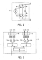
- the supply circuit 1-3 comprises a first circuit 1 and a second circuit 2 and a third circuit 3.
- the first circuit 1 comprises a voltage source 4 for generating an input voltage signal via first and second reference terminals 15 and 16.
- the first circuit 1 further comprises four transistors 11-14.
- a first transistor 11 has a first main electrode coupled to the first reference terminal 15 and has a second main electrode coupled to a first input 20a of the second circuit 2.
- a second transistor 12 has a first main electrode coupled to the second main electrode of the first transistor 11 and has a second main electrode coupled to the second reference terminal 16.
- a third transistor 13 has a first main electrode coupled to the first reference terminal 15 and has a second main electrode coupled to a second input 20b of the second circuit 2.
- a fourth transistor 14 has a first main electrode coupled to the second main electrode of the third transistor 13 and has a second main electrode coupled to the second reference terminal 16.
- the first circuit 1 further comprises logical circuitry 5 coupled to the third circuit 3 and to the control electrodes of the transistors 11-14. This logical circuitry 5 will be discussed referring to the Fig. 3 .
- the second circuit 2 comprises from the input 20a to the input 20b a for example serial resonance circuit of a capacitor 27, an inductance 26 and a primary side of a transformer 25.
- the inductance 26 is usually at least partly formed by a stray inductance of the transformer 25.
- the second circuit 2 possibly further comprises four output diodes 21-24 coupled to a secondary side of the transformer 25 and forming a rectifying circuit that is further coupled to a smoothing capacitor 28 and to a load 6 for example comprising three serial light emitting diodes.
- the AC to DC converter 4 or voltage source 4 shown in Fig. 2 comprises an AC voltage source 45 coupled to four diodes forming a further rectifying circuit that is further coupled to a further smoothing capacitor 46.
- the logical circuitry 5 shown in Fig. 3 comprises a flipflop 51 receiving the control signal from the third circuit 3.
- a Q-output of the flipflop is coupled to an AND gate 52 that further receives the control signal and an inverted Q-output of the flipflop 51 is coupled to an AND gate 53 that further receives the control signal.
- An output of the AND gate 52 is coupled via a non-inverter 52a to a tdon delay circuit 54a and via an inverter 52b to a tdon delay circuit 54b.
- An output of the AND gate 53 is coupled via a non-inverter 53a to a tdon delay circuit 55a and via an inverter 53b to a tdon delay circuit 55b.
- the respective tdon delay circuits 54a and 54b and 55a and 55b are coupled to the control electrodes of the respective transistors 11-14, possibly via a level shifter 56 on behalf of the transistors 11 and 12 and a level shifter 57 on behalf of the transistors 13 and 14.
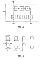
- the third circuit 3 shown in Fig. 4 comprises an input 30a for receiving the input voltage signal Uin (more general: input signal or primary side signal) and comprises an output 30c for supplying the control signal s(t) in dependence of the input voltage signal Uin and independently from the output current signal through the load 6.
- the third circuit 3 further comprises a further input 30b for receiving a reference current signal, the control signal s(t) further depending on the reference current signal.
- the third circuit 3 comprises a multiplier 31 for multiplying the input voltage signal Uin and the control signal s(t) and comprises a low pass filter 32 for low pass filtering a multiplier output voltage signal and comprises a converter 33 for converting a low pass filter output voltage signal into a low pass filter output current signal and comprises an adder 34 for adding an inverted low pass filter output current signal and the reference current signal.
- a generator 35-37 comprises a controller 35 for receiving an adder output current signal and comprises a voltage controlled oscillator 36 for receiving a controller output signal and comprises a monoflop 37 for receiving a voltage controlled oscillator output signal and for generating the control signal s(t).
- the pulse signal U1 has first pulses having a first amplitude +Uin and has second pulses having a second amplitude -Uin different from the first amplitude and has levels having a third amplitude 0 different from the first and second amplitudes.
- the first amplitude is a positive amplitude
- the second amplitude is a negative amplitude
- the third amplitude is a substantially zero amplitude.
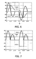
- a current I1(t) through a primary side of the transformer 25 of the second circuit 2 and a voltage Uc(t) across the capacitor 27 of the second circuit 2 as a function of the pulse signal U1(t) are shown.
- a current ID(t) through a secondary side of the transformer 25 of the second circuit 2 (after the rectifier) and a current Iout through the load 6 as a function of the pulse signal U1(t) are shown.
- the device 10 according to the invention shown in Fig. 8 comprises the first and second ands third circuits 1-3 and the load 6 and the voltage source 4 this time located outside the first circuit 1.
- control signal s(t) and individual control signals f1 (output AND gate 53) and f2 (output AND gate 52) and T1-T4 (outputs tdon delay circuits 54a,54b,55a,55b) derived there from by the logical circuitry 5 and destined for the individual transistors 11-14 are shown.
- the input voltage Uin can be a non-stabilized DC voltage.
- the driver consists of a transistor H-bridge 11-14, a controlling third circuit 3 for the H-bridge 11-14, a transformer 25, a series capacitor 27, a diode bridge 21-24 and a smoothing output capacitor 28. At the output, a series connection of LEDs can be supplied.
- the transformer 25 serves for galvanic isolation and may adapt the voltage level, e.g. from 300V to 30V.
- a resonant topology is formed by the stray inductance 26 of the transformer 25 and the series capacitor 27.
- the parasitic leakage inductance of the transformer 25 can be part of the driver.
- the leakage inductance does not need to be minimized. This is of advantage for the isolation and winding design and it thus keeps the cost low.
- the controlling third circuit 3 and the logical circuitry 5 generate alternated positive and negative voltage pulses with a fixed pulse width. Between these voltage pulses the H-bridge 11-14 should stay in a free wheel state for a settable time. Hence, the output is controlled by the repetition frequency. If the resonant frequency of the circuit is properly adapted to the width of the voltage pulse and if the number of LEDs meets the operation voltage range of the circuit, an ideal LED supply driver has been created that shows the following features:
- any none stabilized DC voltage Uin can be used to supply the driver.
- This voltage may be generated from the AC mains by using a further diode bridge 41-44 and a further smoothing capacitor 46.
- the power part of the driver consists of an H-bridge realized by 4 transistors 11-14. These transistors are controlled by the third circuit 3 via the logical circuitry 5. Voltage level shifters may be used as interfaces between the control electrodes of the transistors 11-14 and the logical circuitry 5.
- the output terminals of the H-bridge 11-14 are connected to the primary winding of the transformer 25 via a series capacitor 27.
- the secondary winding of the transformer 25 feeds the diode bridge 21-24.
- This diode bridge 21-24 rectifies the AC voltage from the transformer 25 and a smoothing capacitor 28 is used to smooth the output voltage Uout.
- the series connection of an arbitrary number of LEDs is supplied by the output voltage Uout.
- the H-bridge 11-14 generates alternately positive and negative voltage pulses (+Uin or -Uin). The positive voltage pulse occurs if transistor 11 and transistor 14 are in the on state while the negative voltage pulse can be set turning on the transistors 12 and 13. Between the voltage pulses the H-bridge 11-14 provides a free wheel path, which may be performed either by turning on 11 and 13 or by turning on 12 and 14.
- Fig. 5 shows a characteristic output voltage wave of the H-bridge 11-14 as well as a basic switching function s(t) generated inside the controlling third circuit 3.
- the nominal output voltage Uout may be determined by the number of LEDs connected in series and their voltage drops. It might stay within the voltage range
- shown in Fig. 7 . Because of the smoothing capacitor 28 a DC output current is flowing in the load 6 which is equal to the average value of the rectified secondary current Iout IDrectified.
- the third circuit 3 without excluding other circuits.
- the unsigned voltage pulses to be generated by the switching function s(t) and the input DC voltage Uin are low pass filtered (e.g. by a RC network).
- the resulting DC voltage is proportional to the voltage frequency product.
- This voltage is converted into a current via the converter 33 and is compared with a reference current and the difference sets the operating frequency fs via the controller 35.
- the controller 35 controls the voltage controlled oscillator 36 that generates fs and that triggers the monoflop 37 that generates the control signal s(t) with pulses having a pulse width ton etc.
- ton 1 / (2 fres).
- the turn on delay circuits 54a, 54b, 55a, 55b introduce a time delay tdon for avoiding a short circuit in the H bridge 11-14.
- This invention might be used for wall flooding, LCD backlighting and general illumination, without excluding other applications with loads in the form of LEDs or in the form of non-LEDs.
- the supply circuit according to the invention shown in the Fig. 10 comprises a first circuit 101 comprising a half bridge with a serial transistor circuit of a first transistor 111 and a second transistor 112 coupled to a source Vo and comprises a second circuit 102 comprising a for example serial resonance circuit of a capacitor 127 and an inductor 126.
- One side of the serial resonance circuit is coupled to a common point of the serial transistor circuit and an other side is coupled to first and second (antiparallel) branches.
- the first (second) branch comprises a diode 121A (121B) coupled to a parallel circuit of a capacitor 128A (128B) and for example serially coupled LEDs 106A (106B).
- the half bridge may be replaced by for example a full bridge in a half bridge mode.
- the inductor 126 may be replaced by a transformer of which a primary side is coupled to the capacitor 127 and of which a secondary side is coupled to the branches.
- the supply circuit according to the invention shown in the Fig. 11 comprises a first circuit 101 comprising a half bridge with a serial transistor circuit of a first transistor 111 and a second transistor 112 coupled to a source Vo and comprises a second circuit 102 comprising a for example serial resonance circuit of a capacitor 127 and an inductor 126.
- One side of the serial resonance circuit is coupled to a common point of the serial transistor circuit and an other side is coupled to first and second (antiparallel) branches.
- the first (second) branch comprises a first (second) serial diode-capacitor circuit of a diode 121C (121D) coupled to a capacitor 128C (128D).
- Common points of the serial diode-capacitor circuits are coupled to each other via for example serially coupled LEDs 106C. This is a voltage doubler with a two-capacitor construction.
- the supply circuit according to the invention shown in the Fig. 12 comprises the half bridge with the serial transistor circuit of the first transistor 111 and the second transistor 112 coupled to the source Vo already discussed for the Fig. 10 and 11 and comprises the for example serial resonance circuit of the capacitor 127 and the inductor 126 already discussed for the Fig. 10 and 11 .
- One side of the serial resonance circuit is coupled to a capacitor 128E, which is coupled to an anode of a diode 121E and to a cathode of a diode 121 F.
- These diodes 121E-121F are further coupled to for example serially coupled LEDs 106E. This is a voltage doubler with a one-capacitor construction.
- the supply circuit according to the invention shown in the Fig. 13 corresponds with the supply circuits shown in the Fig. 11 and 12 whereby the voltage doubler construction has been replaced by a Cockroft-Walton multiplier construction.
- a voltage Vin supplied by a first circuit 101 and a voltage Vc across a capacitor 127 as a function of time are shown
- a current through an inductor 126 as a function of time is shown for a switching period being equal to two times the resonance period of 126,127.
- a voltage Vin and a current through an inductor 126 and an averaged current Io1 are shown for a switching period being greater than two times the resonance period of 126,127.
- the topology may be a combination of a half bridge for example driving a series tank and rectifier load branches at or below resonance.
- the topology behaves like a voltage current converter, when for example both the input voltage and the switching frequency are constant then the output current is known, no additional shunts for constant current load driving are required, zero current switching is achieved, a resonant operating mode allows to increase a switching frequency for reducing a volume of passive components, it may work with or without transformer, it has an inherent short circuit protection, it may have integrated magnetics for transformer based solutions whereby a transformer leakage inductance can be used as series tank inductor, it may have a sinusoidal tank current with a low EMI to allow an AC bus, it does not need cross regulation, so i.e. load variation in one output branch does not affect the current in the output, there is an implicit over voltage protection and it may be used to drive a voltage multiplier to increase an output voltage swing without a transformer (important for integration).
- Vo denotes a DC input voltage
- 111 and 112 are for example MosFets of a half bridge
- 127 and 126 are for example series resonant tank elements
- 121 is an output rectifier diode
- 106 is a load string of for example LEDs.
- the response can be subdivided into two states with two subintervals.
- the two states are defined by I) 121 A is on & 121B is off (State I) and by II) 121A is off and 121 B is on (State II).
- the switching period Ts may be chosen to be 4* ⁇ or greater.
- Vo is constant
- the current through the loads is constant as well.
- Even the load & cross regulation error is zero, which i.e. means that voltage changes on one branch do not affect the current neither of the same nor of the other branch.
- the switching frequency may be adapted in such a way that the product of Vo and fs and thus the output current is kept relatively constant as well. This is shown in the Fig. 17 and 18 to be discussed below. So, the for example half-bridge topology behaves like an ideal voltage/current converter. Another important aspect is the peak load current for constant output power.
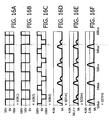
- FIG. 16 voltages and currents for different situations A-F as a function of time are shown, for example for Vout ⁇ Vo.
- E diode current half bridge
- F diode current full bridge with zero state.
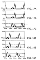
- Fig. 18 currents for different situations A-C as a function of time are shown (all in one graph).
- the current & averaged current in a branch for varying an output voltage in an other branch shows that an averaged current is constant.
- a third circuit may be used for driving the bridge according to one or more of the four driving schemes as defined above, to reduce a dependency between the input signal and the output signal.
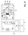
- the supply circuit according to the invention shown in the Fig. 19 comprises a first circuit 201 and a second circuit 202 and a third circuit 203.
- the first circuit 201 comprises a voltage source 204 for generating an input voltage signal Uin via first and second reference terminals 215 and 216.
- the first circuit 201 further comprises two transistors 211-212.
- a first transistor 211 has a first main electrode coupled to the first reference terminal 215 and has a second main electrode coupled to a first input 220a of the second circuit 202.
- a second transistor 212 has a first main electrode coupled to the second main electrode of the first transistor 211 and has a second main electrode coupled to the second reference terminal 216 which is further coupled to a second input 220b of the second circuit 202.
- the first circuit 201 further comprises logical circuitry 205 coupled to the third circuit 203 and to the control electrodes of the transistors 211-212.
- This logical circuitry 205 is for example identical to a part of the logical circuitry 5 discussed before.
- the second circuit 202 is for example identical to the second circuit 2 discussed before.
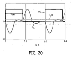
- a voltage Vin and a current through an inductor 126 and an averaged current Io2 are shown for a switching period being greater than two times the resonance period of 126,127.
- T switching frequency
- ton Tres
- Tres resonance period.
- supply circuits 1-3,101-102,201-203 for supplying output current signals to loads 6,106,206 and comprising first circuits 1,101,201 with transistors 11-14, 111-112, 211-212 for converting input voltage signals into pulse signals and comprising second circuits 2,102,202 with resonance circuits for receiving the pulse signals and for supplying the output current signals to the loads 6,106,206 are provided with third circuits 3,203 for controlling the first circuits 1,101,201, which third circuits 3,203 comprise generators 35-37 for generating control signals for controlling the transistors 11-14,111-112,211-212 for reducing dependencies between the input voltage signals and the output current signals.
- the third circuits 3,203 supply the control signals in dependence of the input voltage signals and independently from the output current signals.
- the transistors 11-14,111-112,211-212 may form a full bridge, a full bridge operated in a half bridge mode, or a half bridge.
- the invention may be implemented by means of hardware comprising several distinct elements, and by means of a suitably programmed computer.
- the device claim enumerating several means several of these means may be embodied by one and the same item of hardware.
Landscapes
- Engineering & Computer Science (AREA)
- Power Engineering (AREA)
- Dc-Dc Converters (AREA)
Abstract
Description
- The invention relates to a supply circuit for supplying an output signal to a load, which supply circuit comprises
- a first circuit for converting an input signal into a pulse signal, which first circuit comprises transistors,
- a second circuit for receiving the pulse signal and for supplying the output signal to the load, which second circuit comprises a resonance circuit, and
- a third circuit for controlling the first circuit, which third circuit comprises a generator for generating a control signal for controlling the transistors for reducing a dependency between the input signal and the output signal.
- The invention also relates to a device comprising a supply circuit.
- Examples of such a supply circuit are switched mode power supplies, without excluding other supply circuits. Examples of such a load are one light emitting diode and two or more serial light emitting diodes and two or more parallel light emitting diodes, without excluding other loads.
- A prior art supply circuit is known from
US 6,853,150 B2 , which discloses a supply circuit comprising a transistor circuit with two transistors in a half bridge configuration and comprising an impedance circuit with an inductor and capacitors each coupled to light emitting diodes. - The prior art supply circuit is disadvantageous, inter alia, in that a fluctuation in an input signal and/or a fluctuation in a voltage drop across the light emitting diodes may result in a fluctuation in an output signal, which may result in a fluctuation in a brightness of a light emitting diode.
-
US 2005 / 0073859 discloses a DC/AC converter and a controller integrated circuit. -
EP 0 317 698 -
US 2004 / 0183380 discloses a switching constant-current power supply system. -
US 2005 / 0281061 discloses a resonance converter with voltage regulation. - An article Full-Bridge Current-Fed Inverter with Automatic Frequency Control for Forging Application, by S. CHUDJUARJEEN, C. KOOMPAI and V. MONYAKUL discloses a full-bridge current-fed inverter with an automatic frequency control (XP 002447510).
-
US 6,420,858 discloses a DC-to-DC converter circuit having a power saving mode. - It is an object of the invention, inter alia, to provide a supply circuit that supplies a relatively constant output signal to a load.
- Further objects of the invention are, inter alia, to provide a device comprising a supply circuit that supplies a relatively constant output signal to a load.
- According to the invention, the supply circuit for supplying an output signal to a load is defined according to
claim 1. - By introducing, in addition to the first circuit and the second circuit, the third circuit for controlling the first circuit, which third circuit comprises the generator for generating the control signal for controlling the transistors in such a way that a dependency between the input signal and the output signal is reduced, the supply circuit according to the invention supplies a relatively constant output signal to a load.
- The input signal for example comprises an input voltage signal, without excluding other input signals, and the output signal for example comprises an output current signal, without excluding other output signals.
- The supply circuit according to the invention further reduces a dependency between for example an output voltage signal and for example an output current signal.
- The third circuit comprises an input for receiving the input signal and comprising an output for supplying the control signal in dependence of the input signal and independently from the output signal, to advantageously avoid a use of a disadvantageous feedback loop from the load (secondary side) to the first circuit (primary side). In other words, the control signal is supplied in dependence of a primary side signal and independently from a secondary side signal.
- The reference signal for example comprises a reference current signal, without excluding other reference signals.
- The third circuit comprises a control loop. The addition of the inversion of the converter output signal and the reference signal of course corresponds with a subtraction of the converter output signal from the reference signal. The multiplier output signal for example comprises a multiplier output voltage signal, the low pass filter output signal for example comprises a low pass filter output voltage signal before entering the converter and for example comprises a low pass filter output current signal after having left the converter and the adder output signal for example comprises an adder output current signal, without excluding other signals.
- An embodiment of the supply circuit according to the invention is defined by the pulse signal comprising first pulses having a first amplitude and comprising second pulses having a second amplitude different from the first amplitude and comprising levels having a third amplitude different from the first and second amplitudes. This embodiment advantageously introduces a pulse signal with three different amplitudes that increase a number of controlling options.
- Preferably, the supply circuit according to the invention is defined by the first amplitude being a positive amplitude, the second amplitude being a negative amplitude, and the third amplitude being a substantially zero amplitude. This embodiment advantageously introduces a symmetrical pulse signal.
- Preferably, the supply circuit according to the invention is defined by the first circuit comprising a first transistor having a first main electrode coupled to a first reference terminal and having a second main electrode coupled to a first input of the second circuit and comprising a second transistor having a first main electrode coupled to the second main electrode of the first transistor and having a second main electrode coupled to a second reference terminal and comprising a third transistor having a first main electrode coupled to the first reference terminal and having a second main electrode coupled to a second input of the second circuit and comprising a fourth transistor having a first main electrode coupled to the second main electrode of the third transistor and having a second main electrode coupled to the second reference terminal. This embodiment advantageously introduces a first circuit comprising four transistors in a full bridge configuration (H bridge).
- Preferably, the supply circuit according to the invention is defined by the first circuit comprising logical circuitry for receiving the control signal and comprising outputs coupled to control electrodes of the transistors for bringing the first and fourth transistors in a conducting state to create the first pulses and for bringing the second and third transistors in a conducting state to create the second pulses and for bringing either the first and third or the second and fourth transistors in a conducting state to create the levels. This embodiment advantageously introduces logical circuitry into the first circuit for coupling the first and third circuits to each other.
- An embodiment of the supply circuit according to the invention is defined by the pulse signal comprising first pulses having a first amplitude and comprising second pulses having a second amplitude different from the first amplitude. This embodiment advantageously introduces a pulse signal with only two different amplitudes.
- Preferably, the supply circuit according to the invention is defined by the first amplitude being a positive amplitude and the second amplitude being a negative amplitude. This embodiment advantageously introduces a symmetrical pulse signal.
- Preferably, the supply circuit according to the invention is defined by the first circuit comprising the four transistor topology described above, which four transistors are operated in such a way that now only a pulse signal with two different amplitudes is introduced. This embodiment advantageously introduces a first circuit comprising four transistors in a full bridge configuration (H bridge) that now introduce a pulse signal with only two amplitudes.
- An embodiment of the supply circuit according to the invention is defined by the pulse signal comprising third pulses having a fourth amplitude and comprising a level having a fifth amplitude. This embodiment advantageously introduces a pulse signal with only two different amplitudes, one of these amplitudes being realized by a pulse and the other one of these amplitudes being realized by a level.
- Preferably, the supply circuit according to the invention is defined by the fourth amplitude being a positive amplitude and the fifth amplitude being a substantially zero amplitude. This embodiment advantageously introduces an asymmetrical pulse signal.
- Preferably, the supply circuit according to the invention is defined by the first circuit comprising a first transistor having a first main electrode coupled to a first reference terminal and having a second main electrode coupled to a first input of the second circuit and comprising a second transistor having a first main electrode coupled to the second main electrode of the first transistor and having a second main electrode coupled to a second reference terminal, which second reference terminal is further coupled to a second input of the second circuit. This embodiment advantageously introduces a first circuit comprising two transistors in a half bridge configuration.
- Preferably, the supply circuit according to the invention is defined by the first circuit comprising logical circuitry for receiving the control signal and comprising outputs coupled to control electrodes of the transistors for bringing the first transistor in a conducting state to create the third pulses and for bringing the second transistor in a conducting state to create the levels. This embodiment advantageously introduces logical circuitry into the first circuit for coupling the first and third circuits to each other.
- Preferably, the supply circuit according to the invention is defined by the first circuit comprising a half bridge, and the third circuit being arranged to drive the half bridge at Ts≥4*tau, where tau is half a resonance period of the resonance circuit and Ts is a switching period.
- Preferably, the supply circuit according to the invention is defined by the first circuit comprising a full bridge, and the third circuit being arranged to drive the full bridge as either a half bridge at an on&off time=2*tau and at Ts≥4*tau or as a full bridge without a free wheel state at an on+&on-time=2*tau and at Ts≥4*tau or as a full bridge with a free wheel state at on+&on-time=tau and free wheel states of length tau following every pulse and Ts≥4*tau, where tau is half a resonance period of the resonance circuit and Ts is a switching period.
- An embodiment of the supply circuit according to the invention is defined by the resonance circuit comprising a transformer and a capacitor coupled serially to a primary side of the transformer or to a secondary side of the transformer. This embodiment advantageously introduces the transformer for providing galvanic isolation. Possibly, the second circuit may further comprise a rectifying circuit comprising one or more diodes coupled to a secondary side of the transformer. This embodiment advantageously further introduces the capacitor for in combination with the leakage inductance of the transformer (and/or with a separate inductor) creating a resonant circuit.
- An embodiment of the supply circuit according to the invention is defined by the resonance circuit comprising an inductor and a capacitor coupled serially to a primary side of the inductor or to a secondary side of the inductor. This embodiment advantageously introduces the inductor. Such an inductor is more low cost than a transformer. Possibly, the second circuit may further comprise a rectifying circuit comprising one or more diodes coupled to a secondary side of the inductor. This embodiment advantageously further introduces the capacitor for in combination with the inductor creating a resonant circuit.
- An embodiment of the supply circuit according to the invention is defined by the load comprising one or more light emitting diodes.
- An embodiment of the supply circuit according to the invention is defined by comprising one or more input diodes for rectifying an AC signal, the input signal comprising a rectified AC signal. The AC signal for example comprises an AC voltage signal, without excluding other AC signals.
- An embodiment of the supply circuit according to the invention is defined by a pulse of the pulses having a pulse width substantially equal to half a resonant period of the resonance circuit (full bridge).
- An embodiment of the supply circuit according to the invention is defined by the pulse frequency being substantially equal to or smaller than half a resonant frequency of the resonance circuit (full bridge).
- The product of the input signal and the pulse frequency is substantially constant. This way, a constant output current signal is generated that is independent from an input voltage signal.
- An embodiment of the supply circuit according to the invention is defined by a pulse of the pulses having a pulse width substantially equal to a resonant period of the resonance circuit (half bridge).
- An embodiment of the supply circuit according to the invention is defined by the pulse frequency being substantially equal to or smaller than a resonant frequency of the resonance circuit (half bridge).
- The product of the input signal and the pulse frequency is substantially constant. This way, a constant output current signal is generated that is independent from an input voltage signal.
- Embodiments of the device according to the invention correspond with the embodiments of the supply circuit according to the invention.
- The invention is based on the insight, inter alia, that a fluctuation in an input voltage may result in a fluctuation in an output current which is to be avoided, and is based on the basic idea, inter alia, that in addition to the first circuit and the second circuit, the third circuit for controlling the first circuit in such a way that a dependency between the input signal and the output signal is reduced is to be introduced.
- The invention solves the problem, inter alia, to provide a supply circuit that supplies a relatively constant output signal to a load, and is further advantageous, inter alia, in that a dependency between for example an output voltage signal and for example an output current signal is reduced.
- These and other aspects of the invention will be apparent from and elucidated with reference to the embodiments(s) described hereinafter.
- In the drawings:
-
Fig. 1 shows diagrammatically a supply circuit according to the invention comprising first and second and third circuits, -
Fig. 2 shows diagrammatically an AC to DC converter, -
Fig. 3 shows logical circuitry for the first circuit, -
Fig. 4 shows the third circuit in greater detail, -
Fig. 5 shows a control signal and a resulting pulse signal, -
Fig. 6 shows a current through a primary side of a transformer of the second circuit and a voltage across a capacitor of the second circuit as a function of the pulse signal, -
Fig. 7 shows a current through a secondary side of the transformer of the second circuit and a current through the load as a function of the pulse signal, -
Fig. 8 shows a device according to the invention, -
Fig. 9 shows the control signal and individual control signals derived therefrom by the logical circuitry and destined for the individual transistors, -
Fig. 10 shows diagrammatically another supply circuit according to the invention, -
Fig. 11 shows diagrammatically another supply circuit according to the invention, -
Fig. 12 shows diagrammatically another supply circuit according to the invention, -
Fig. 13 shows diagrammatically another supply circuit according to the invention, -
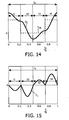
Fig. 14 shows a voltage supplied by a first circuit and a voltage across a capacitor as a function of time, -
Fig. 15 shows a current through an inductor as a function of time, -
Fig. 16 shows voltages and currents for different situations A-F as a function of time, -
Fig. 17 shows currents for different situations A-C as a function of time, -
Fig. 18 shows currents for different situations A-C as a function of time, -
Fig. 19 shows diagrammatically another supply circuit according to the invention, and -
Fig. 20 shows currents and voltage for a switching period as a function of time (Ts>4*tau), tau = half resonant period. - The supply circuit 1-3 according to the invention shown in
Fig. 1 comprises afirst circuit 1 and asecond circuit 2 and athird circuit 3. Thefirst circuit 1 comprises avoltage source 4 for generating an input voltage signal via first andsecond reference terminals first circuit 1 further comprises four transistors 11-14. Afirst transistor 11 has a first main electrode coupled to thefirst reference terminal 15 and has a second main electrode coupled to afirst input 20a of thesecond circuit 2. Asecond transistor 12 has a first main electrode coupled to the second main electrode of thefirst transistor 11 and has a second main electrode coupled to thesecond reference terminal 16. Athird transistor 13 has a first main electrode coupled to thefirst reference terminal 15 and has a second main electrode coupled to asecond input 20b of thesecond circuit 2. Afourth transistor 14 has a first main electrode coupled to the second main electrode of thethird transistor 13 and has a second main electrode coupled to thesecond reference terminal 16. Thefirst circuit 1 further compriseslogical circuitry 5 coupled to thethird circuit 3 and to the control electrodes of the transistors 11-14. Thislogical circuitry 5 will be discussed referring to theFig. 3 . - The
second circuit 2 comprises from theinput 20a to theinput 20b a for example serial resonance circuit of acapacitor 27, aninductance 26 and a primary side of atransformer 25. Theinductance 26 is usually at least partly formed by a stray inductance of thetransformer 25. Thesecond circuit 2 possibly further comprises four output diodes 21-24 coupled to a secondary side of thetransformer 25 and forming a rectifying circuit that is further coupled to a smoothing capacitor 28 and to aload 6 for example comprising three serial light emitting diodes. - The AC to
DC converter 4 orvoltage source 4 shown inFig. 2 comprises anAC voltage source 45 coupled to four diodes forming a further rectifying circuit that is further coupled to a further smoothingcapacitor 46. - The
logical circuitry 5 shown inFig. 3 comprises aflipflop 51 receiving the control signal from thethird circuit 3. A Q-output of the flipflop is coupled to an ANDgate 52 that further receives the control signal and an inverted Q-output of theflipflop 51 is coupled to an ANDgate 53 that further receives the control signal. An output of the ANDgate 52 is coupled via a non-inverter 52a to a tdon delay circuit 54a and via aninverter 52b to a tdon delay circuit 54b. An output of the ANDgate 53 is coupled via a non-inverter 53a to atdon delay circuit 55a and via aninverter 53b to atdon delay circuit 55b. The respectivetdon delay circuits level shifter 56 on behalf of thetransistors level shifter 57 on behalf of thetransistors - The
third circuit 3 shown inFig. 4 comprises aninput 30a for receiving the input voltage signal Uin (more general: input signal or primary side signal) and comprises anoutput 30c for supplying the control signal s(t) in dependence of the input voltage signal Uin and independently from the output current signal through theload 6. Thethird circuit 3 further comprises afurther input 30b for receiving a reference current signal, the control signal s(t) further depending on the reference current signal. Thereto, thethird circuit 3 comprises amultiplier 31 for multiplying the input voltage signal Uin and the control signal s(t) and comprises alow pass filter 32 for low pass filtering a multiplier output voltage signal and comprises aconverter 33 for converting a low pass filter output voltage signal into a low pass filter output current signal and comprises anadder 34 for adding an inverted low pass filter output current signal and the reference current signal. A generator 35-37 comprises a controller 35 for receiving an adder output current signal and comprises a voltage controlled oscillator 36 for receiving a controller output signal and comprises a monoflop 37 for receiving a voltage controlled oscillator output signal and for generating the control signal s(t). - In
Fig. 5 , the control signal s(t) and a resulting pulse signal U1(t) are shown. The pulse signal U1 has first pulses having a first amplitude +Uin and has second pulses having a second amplitude -Uin different from the first amplitude and has levels having athird amplitude 0 different from the first and second amplitudes. Preferably, the first amplitude is a positive amplitude, the second amplitude is a negative amplitude, and the third amplitude is a substantially zero amplitude. - In
Fig. 6 , a current I1(t) through a primary side of thetransformer 25 of thesecond circuit 2 and a voltage Uc(t) across thecapacitor 27 of thesecond circuit 2 as a function of the pulse signal U1(t) are shown. - In
Fig. 7 , a current ID(t) through a secondary side of thetransformer 25 of the second circuit 2 (after the rectifier) and a current Iout through theload 6 as a function of the pulse signal U1(t) are shown. - The
device 10 according to the invention shown inFig. 8 comprises the first and second ands third circuits 1-3 and theload 6 and thevoltage source 4 this time located outside thefirst circuit 1. - In
Fig. 9 , the control signal s(t) and individual control signals f1 (output AND gate 53) and f2 (output AND gate 52) and T1-T4 (outputstdon delay circuits logical circuitry 5 and destined for the individual transistors 11-14 are shown. - In general, a galvanic isolating driver topology and a control scheme for Light Emitting Diodes or LEDs have been created. The input voltage Uin can be a non-stabilized DC voltage. The driver consists of a transistor H-bridge 11-14, a controlling
third circuit 3 for the H-bridge 11-14, atransformer 25, aseries capacitor 27, a diode bridge 21-24 and a smoothing output capacitor 28. At the output, a series connection of LEDs can be supplied. - The
transformer 25 serves for galvanic isolation and may adapt the voltage level, e.g. from 300V to 30V. A resonant topology is formed by thestray inductance 26 of thetransformer 25 and theseries capacitor 27. Thus, the parasitic leakage inductance of thetransformer 25 can be part of the driver. Contrary to Pulse Width Modulation based converters such as forward or fly back topologies, here the leakage inductance does not need to be minimized. This is of advantage for the isolation and winding design and it thus keeps the cost low. - The controlling
third circuit 3 and thelogical circuitry 5 generate alternated positive and negative voltage pulses with a fixed pulse width. Between these voltage pulses the H-bridge 11-14 should stay in a free wheel state for a settable time. Hence, the output is controlled by the repetition frequency. If the resonant frequency of the circuit is properly adapted to the width of the voltage pulse and if the number of LEDs meets the operation voltage range of the circuit, an ideal LED supply driver has been created that shows the following features: - The current in the driver becomes sinusoidal and it is zero at the switching instants. This avoids switching losses and minimizes EMI.
- The average current in the LEDs is proportional to the DC input voltage of the driver and to the operating frequency. This means the voltage drops of the LEDs do not affect the current over a large load range. If the product of the DC input voltage times the frequency is kept constant, the average current in the LEDs is constant as well. Moreover the LED current can be varied from a nominal value down to zero.
- The LED driver system neither requires sensors nor control units on the secondary (LED) side.
- Changes of the LED parameters do not affect the current in the LEDs. This also includes a short circuit of a single LED. The overall voltage drop of all LEDs may vary between 33% to 100%.
- The nominal output voltage can be set by the turn ratio of the
transformer 25. - The lighting system is very suitable for mains supply.
- A dimming function can easily be installed.
- The power and control unit can be integrated in a smart power IC.
- More in particular, any none stabilized DC voltage Uin can be used to supply the driver. This voltage may be generated from the AC mains by using a further diode bridge 41-44 and a further smoothing
capacitor 46. The power part of the driver consists of an H-bridge realized by 4 transistors 11-14. These transistors are controlled by thethird circuit 3 via thelogical circuitry 5. Voltage level shifters may be used as interfaces between the control electrodes of the transistors 11-14 and thelogical circuitry 5. - The output terminals of the H-bridge 11-14 are connected to the primary winding of the
transformer 25 via aseries capacitor 27. The secondary winding of thetransformer 25 feeds the diode bridge 21-24. This diode bridge 21-24 rectifies the AC voltage from thetransformer 25 and a smoothing capacitor 28 is used to smooth the output voltage Uout. The series connection of an arbitrary number of LEDs is supplied by the output voltage Uout. - The
series capacitor 27 and thestray inductance 26 of thetransformer 25 form a series resonant circuit with a resonant frequency fres = (2π)-1 (L26C27)-½ = (Tres)-1 and with a resonant impedance Zres = (L26/C27)-½. The H-bridge 11-14 generates alternately positive and negative voltage pulses (+Uin or -Uin). The positive voltage pulse occurs iftransistor 11 andtransistor 14 are in the on state while the negative voltage pulse can be set turning on thetransistors - In case the pulse width ton is fixed, the frequency fs can be used as a control parameter. Its maximum value has to be limited to fmax = fres/2 > fs.
Fig. 5 shows a characteristic output voltage wave of the H-bridge 11-14 as well as a basic switching function s(t) generated inside the controllingthird circuit 3. - The nominal output voltage Uout may be determined by the number of LEDs connected in series and their voltage drops. It might stay within the voltage range
- N2 Uin / (3 N1) < Uout < N2 Uin / N1, whereby N2 represents the secondary windings and N1 represents the primary windings of the
transformer 25. If the conditions are fulfilled, two successive sinusoidal half-wave current pulses are drawn from the H-bridge 11-14 for each voltage pulse. The corresponding current I1(t) is presented inFig. 6 for a certain operation point. Moreover this picture also illustrates the resulting voltage Uc(t) at theseries capacitor 27. - Neglecting the magnetization current, the secondary current of the
transformer 25 is proportional to the primary current I2 = I1 N1 / N2. The secondary transformer current I2 is rectified by the diode bridge 21-24, with ID(t) = | I2(t) | shown inFig. 7 . Because of the smoothing capacitor 28 a DC output current is flowing in theload 6 which is equal to the average value of the rectified secondary current Iout = IDrectified. - The output current and thus the LED current is proportional to the frequency and the input voltage: Iout = 2 Uin N1 fs / (Zres π N2 fres). Since the input voltage Uin varies with the mains voltage and because of a voltage ripple caused by a small further smoothing
capacitor 46, the frequency fs may be adapted in such a way that the product of Uin and fs and thus the output current Iout is kept relatively constant. - This can be achieved by the
third circuit 3 without excluding other circuits. In a first step the unsigned voltage pulses to be generated by the switching function s(t) and the input DC voltage Uin are low pass filtered (e.g. by a RC network). The resulting DC voltage is proportional to the voltage frequency product. This voltage is converted into a current via theconverter 33 and is compared with a reference current and the difference sets the operating frequency fs via the controller 35. Thereto, the controller 35 controls the voltage controlled oscillator 36 that generates fs and that triggers the monoflop 37 that generates the control signal s(t) with pulses having a pulse width ton etc. Preferably, but not exclusively, ton = 1 / (2 fres). The turn ondelay circuits - Possible modifications are:
- Instead of MOSFETs any other transistor technology may be used.
- The smoothing capacitor 28 connected in parallel to the LEDs can be omitted. This has no influence on the average current but it increases the RMS and peak current of the LEDs.
- The free-wheel path of the H-bridge 11-14 could always be realized by turning on 12 and 14. In this case the turn on time of the
upper transistors - The
series capacitor 27 could also be inserted on the secondary transformer side or series capacitors may be used on both sides. - The input rectifier may be realized by a PFC rectifier circuit.
- The driver may be realized without a
transformer 25 but with an inductor such as a series choke for forming the resonant topology. - The full bridge output rectifier 21-24 could also be replaced by a combination of split output winding plus only two diodes with the benefit of saving two diodes and having less diode forward conduction losses (but at the price of needing a second winding and perhaps getting asymmetric LED peak currents for the positive and negative transformer input voltage).
- This invention might be used for wall flooding, LCD backlighting and general illumination, without excluding other applications with loads in the form of LEDs or in the form of non-LEDs.
- The supply circuit according to the invention shown in the
Fig. 10 comprises afirst circuit 101 comprising a half bridge with a serial transistor circuit of afirst transistor 111 and asecond transistor 112 coupled to a source Vo and comprises asecond circuit 102 comprising a for example serial resonance circuit of acapacitor 127 and aninductor 126. One side of the serial resonance circuit is coupled to a common point of the serial transistor circuit and an other side is coupled to first and second (antiparallel) branches. The first (second) branch comprises adiode 121A (121B) coupled to a parallel circuit of a capacitor 128A (128B) and for example serially coupledLEDs 106A (106B). - Alternatively, the half bridge may be replaced by for example a full bridge in a half bridge mode. Further alternatively, the
inductor 126 may be replaced by a transformer of which a primary side is coupled to thecapacitor 127 and of which a secondary side is coupled to the branches. - The supply circuit according to the invention shown in the
Fig. 11 comprises afirst circuit 101 comprising a half bridge with a serial transistor circuit of afirst transistor 111 and asecond transistor 112 coupled to a source Vo and comprises asecond circuit 102 comprising a for example serial resonance circuit of acapacitor 127 and aninductor 126. One side of the serial resonance circuit is coupled to a common point of the serial transistor circuit and an other side is coupled to first and second (antiparallel) branches. The first (second) branch comprises a first (second) serial diode-capacitor circuit of adiode 121C (121D) coupled to acapacitor 128C (128D). Common points of the serial diode-capacitor circuits are coupled to each other via for example serially coupledLEDs 106C. This is a voltage doubler with a two-capacitor construction. - The supply circuit according to the invention shown in the
Fig. 12 comprises the half bridge with the serial transistor circuit of thefirst transistor 111 and thesecond transistor 112 coupled to the source Vo already discussed for theFig. 10 and 11 and comprises the for example serial resonance circuit of thecapacitor 127 and theinductor 126 already discussed for theFig. 10 and 11 . One side of the serial resonance circuit is coupled to acapacitor 128E, which is coupled to an anode of adiode 121E and to a cathode of a diode 121 F. Thesediodes 121E-121F are further coupled to for example serially coupledLEDs 106E. This is a voltage doubler with a one-capacitor construction. - The supply circuit according to the invention shown in the
Fig. 13 corresponds with the supply circuits shown in theFig. 11 and12 whereby the voltage doubler construction has been replaced by a Cockroft-Walton multiplier construction. - In the
Fig. 14 , a voltage Vin supplied by afirst circuit 101 and a voltage Vc across acapacitor 127 as a function of time are shown, and in theFig. 15 , a current through aninductor 126 as a function of time is shown for a switching period being equal to two times the resonance period of 126,127. In theFig. 20 a voltage Vin and a current through aninductor 126 and an averaged current Io1 are shown for a switching period being greater than two times the resonance period of 126,127. - The topology may be a combination of a half bridge for example driving a series tank and rectifier load branches at or below resonance. Thereby, the topology behaves like a voltage current converter, when for example both the input voltage and the switching frequency are constant then the output current is known, no additional shunts for constant current load driving are required, zero current switching is achieved, a resonant operating mode allows to increase a switching frequency for reducing a volume of passive components, it may work with or without transformer, it has an inherent short circuit protection, it may have integrated magnetics for transformer based solutions whereby a transformer leakage inductance can be used as series tank inductor, it may have a sinusoidal tank current with a low EMI to allow an AC bus, it does not need cross regulation, so i.e. load variation in one output branch does not affect the current in the output, there is an implicit over voltage protection and it may be used to drive a voltage multiplier to increase an output voltage swing without a transformer (important for integration).
- In the
Fig. 10-15 , Vo denotes a DC input voltage, 111 and 112 are for example MosFets of a half bridge, 127 and 126 are for example series resonant tank elements, 121 is an output rectifier diode, 106 is a load string of for example LEDs. - In view of the
Fig. 10 ,14 and 15 , for a steady state, the response can be subdivided into two states with two subintervals. The two states are defined by I) 121 A is on & 121B is off (State I) and by II) 121A is off and 121 B is on (State II). Thesubintervals Fig. 14 and 15 may be of the same length: t1=t2= t3= t4 = τ, where τ denotes a resonance period: τ=π*√(L1*C1). The switching period Ts may be chosen to be 4*τ or greater. Setting up differential network equations for both states, observing continuity and periodicity conditions the relevant currents and voltages can be calculated analytically. Of importance may be the relations for the averaged current over one switching period Ts=1/fs in both load branches for each state: iavI=iavII=2/π*Vo/Zo*fs/fres, with Zo=√(L1/C1). - This equation shows, that the averaged output current is proportional to a product of the input dc voltage Vo and the switching frequency fs:
- If Vo is constant, the current through the loads is constant as well. Even the load & cross regulation error is zero, which i.e. means that voltage changes on one branch do not affect the current neither of the same nor of the other branch. If the input voltage varies then the switching frequency may be adapted in such a way that the product of Vo and fs and thus the output current is kept relatively constant as well. This is shown in the
Fig. 17 and 18 to be discussed below. So, the for example half-bridge topology behaves like an ideal voltage/current converter. Another important aspect is the peak load current for constant output power. Because the converter oscillates at resonance and the switching period is 4τ there are 2 local current peaks in each state:
Vout2)/Zo|. It may be desirable to have both peaks balanced, i.e. more or less of the same size so that the peak current stress for a given power (averaged current) is minimum. Observing both expressions for the peak current of the converter according to the invention it can be seen that both values are balanced when the output voltages Vout1, Vout2 are small compared to Vo. This implies the proposed converter is perfectly suited for applications with small supply voltages like high power diodes where only a few LEDs are connected in series. - In the
Fig. 16 , voltages and currents for different situations A-F as a function of time are shown, for example for Vout<<Vo. A: input voltage full bridge without zero state, B: input voltage half bridge, C: input voltage full bridge with zero state, D: diode current full bridge without zero state, E: diode current half bridge, and F: diode current full bridge with zero state. - In the
Fig. 17 , currents for different situations A-C as a function of time are shown (cross regulation). The current & averaged current in a branch with a diode for varying an output voltage in a same branch shows that an averaged current is constant. Load parameter is 1d=0,0.5,1 with Vout1=1d*Vout, Vout2=Vout, Vout=48V, Vin=100V. - In the
Fig. 18 , currents for different situations A-C as a function of time are shown (all in one graph). The current & averaged current in a branch for varying an output voltage in an other branch shows that an averaged current is constant. Parameter is ld=0,0.5,1 with Vout1=ld*Vout; Vout2=Vout, Vout=48V and Vin=100V. - So, a for example half bridge topology with a for example series resonant tank and for example rectified outputs has been created with for example dual one-way rectification and with for example a capacitor-diode voltage multiplier for example driven at Ts≥4*tau, where tau=pi*sqrt(L*C). Alternatively, a full bridge with variable driving may be introduced so that the full bridge is driven as either a half bridge (on & off time: 2*tau, Ts≥4*tau) or as a full bridge without a free wheel state (on+ and on-
time 2*tau, Ts≥4*tau) or as a full bridge with a free wheel state (on+ & on-time=tau, free wheel state=tau following every pulse, Ts≥4*tau). In other words, although not shown in theFig. 10-13 , a third circuit may be used for driving the bridge according to one or more of the four driving schemes as defined above, to reduce a dependency between the input signal and the output signal. - The supply circuit according to the invention shown in the
Fig. 19 comprises afirst circuit 201 and asecond circuit 202 and athird circuit 203. Thefirst circuit 201 comprises avoltage source 204 for generating an input voltage signal Uin via first andsecond reference terminals first circuit 201 further comprises two transistors 211-212. Afirst transistor 211 has a first main electrode coupled to thefirst reference terminal 215 and has a second main electrode coupled to afirst input 220a of thesecond circuit 202. Asecond transistor 212 has a first main electrode coupled to the second main electrode of thefirst transistor 211 and has a second main electrode coupled to thesecond reference terminal 216 which is further coupled to asecond input 220b of thesecond circuit 202. Thefirst circuit 201 further compriseslogical circuitry 205 coupled to thethird circuit 203 and to the control electrodes of the transistors 211-212. Thislogical circuitry 205 is for example identical to a part of thelogical circuitry 5 discussed before. Thesecond circuit 202 is for example identical to thesecond circuit 2 discussed before. - In the
Fig. 20 , a voltage Vin and a current through aninductor 126 and an averaged current Io2 are shown for a switching period being greater than two times the resonance period of 126,127. T = switching frequency, ton=Tres where Tres = resonance period. - This
Fig. 20 shows a timing for T>2*Tres, where ton=Tres and Toff>Tres. A minimum timing is T=2*Tres, where ton=Tres and Toff=Tres (as shown inFig.14-15 ). - Summarizing, supply circuits 1-3,101-102,201-203 for supplying output current signals to loads 6,106,206 and comprising first circuits 1,101,201 with transistors 11-14, 111-112, 211-212 for converting input voltage signals into pulse signals and comprising second circuits 2,102,202 with resonance circuits for receiving the pulse signals and for supplying the output current signals to the loads 6,106,206 are provided with third circuits 3,203 for controlling the first circuits 1,101,201, which third circuits 3,203 comprise generators 35-37 for generating control signals for controlling the transistors 11-14,111-112,211-212 for reducing dependencies between the input voltage signals and the output current signals. The third circuits 3,203 supply the control signals in dependence of the input voltage signals and independently from the output current signals. The transistors 11-14,111-112,211-212 may form a full bridge, a full bridge operated in a half bridge mode, or a half bridge.
- Terms like "relatively" and "substantially" define maximum deviations of 30%, preferably 20%, further preferably 10%, most preferably 1%. In other words, such terms define intervals of 70-130%, preferably 80-120%, further preferably 90-110%, most preferably 99-101%.
- The invention may be implemented by means of hardware comprising several distinct elements, and by means of a suitably programmed computer. In the device claim enumerating several means, several of these means may be embodied by one and the same item of hardware.
Claims (10)
- Supply circuit (1-3,101-102,201-203) for supplying an output signal to a load (6,106,206), which supply circuit (1-3,101-102,201-203) comprises- a first circuit (1,101,201) for converting an input signal into a pulse signal, which first circuit comprises transistors (11-14,111-112,211-212),- a second circuit (2,102,202) for receiving the pulse signal and for supplying the output signal to the load (6,106,206), which second circuit (2,102,202) comprises a resonance circuit, and- a third circuit (3,203) for controlling the first circuit (1,101,201), which third circuit (3,203) comprises a generator (35-37) for generating a control signal for controlling the transistors (11-14,111-112,211-212) for reducing a dependency between the input signal and the output signal,
characterized in that the third circuit (3) comprises- an input (30a) for receiving the input signal;- an output (30c) for supplying the control signal in dependence of the input signal and independently from the output signal,wherein the third circuit (3) is arranged to adapt a pulse frequency of pulses of the pulse signal in such a way that, when the input signal varies, a product of the input signal and
the pulse frequency is kept substantially constant,
the third circuit (3) further comprising:- a further input (30b) for receiving a reference current signal, the control signal further depending on the reference current signal;- a multiplier (31) for multiplying the input signal and the control signal and providing a multiplier output signal;- a low pass filter (32) for low pass filtering the multiplier output signal and providing a low pass filter output voltage signal;- a converter (33) for converting the low pass filter output voltage signal and providing a low pass filter output current signal; and- an adder (34) for adding an inversion of the low pass filter output current signal and the reference current signal and providing an adder output signal,wherein the generator (35-37) further comprises:- a controller (35) for receiving the adder output signal and providing a controller output signal;- a voltage controlled oscillator (36) for receiving the controller output signal and providing a voltage controlled oscillator output signal; and- a monoflop (37) for receiving the voltage controlled oscillator output signal and for generating the control signal. - Supply circuit (1-3) as defined in claim 1, the pulse signal comprising first pulses having a first amplitude (+Uin) and comprising second pulses having a second amplitude (-Uin) different from the first amplitude and comprising levels having a third amplitude different from the first and second amplitudes.
- Supply circuit (1-3) as defined in claim 1, the pulse signal comprising first pulses having a first amplitude and comprising second pulses having a second amplitude different from the first amplitude.
- Supply circuit (101-102,201-203) as defined in claim 1, the pulse signal comprising third pulses having a fourth amplitude and comprising a level having a fifth amplitude.
- Supply circuit (1-3,201-203) as defined in claim 1, the resonance circuit comprising a transformer (25,225) and a capacitor (27,227) coupled serially to a primary side of the transformer (25,225) or to a secondary side of the transformer (25,225).
- Supply circuit (101-102) as defined in claim 1, the resonance circuit comprising an inductor (126) and a capacitor (127) coupled serially to a primary side of the inductor (126) or to a secondary side of the inductor (126).
- Supply circuit (1-3) as defined in claim 1, comprising one or more input diodes (41-44) for rectifying an AC signal, the input signal comprising a rectified AC signal.
- Supply circuit (1-3,101-102,201-203) as defined in claim 1, a pulse of the pulses having a pulse width substantially equal to half a resonant period of the resonance circuit or to a resonant period of the resonance circuit.
- Supply circuit (1-3,101-102,201-203) as defined in claim 1, the pulse frequency being substantially equal to or smaller than half a resonant frequency of the resonance circuit or being substantially equal to or smaller than a resonant frequency of the resonance circuit.
- Device (10) comprising the supply circuit (1-3,101-102,201-203) as defined in claim 1 and further comprising the load (6,106,206).
Priority Applications (1)
| Application Number | Priority Date | Filing Date | Title |
|---|---|---|---|
| EP07735026A EP1994635B1 (en) | 2006-03-06 | 2007-03-02 | Supply circuit and device comprising a supply circuit |
Applications Claiming Priority (3)
| Application Number | Priority Date | Filing Date | Title |
|---|---|---|---|
| EP06110730 | 2006-03-06 | ||
| PCT/IB2007/050681 WO2007102106A2 (en) | 2006-03-06 | 2007-03-02 | Supply circuit and device comprising a supply circuit |
| EP07735026A EP1994635B1 (en) | 2006-03-06 | 2007-03-02 | Supply circuit and device comprising a supply circuit |
Publications (2)
| Publication Number | Publication Date |
|---|---|
| EP1994635A2 EP1994635A2 (en) | 2008-11-26 |
| EP1994635B1 true EP1994635B1 (en) | 2012-06-27 |
Family
ID=38349519
Family Applications (1)
| Application Number | Title | Priority Date | Filing Date |
|---|---|---|---|
| EP07735026A Not-in-force EP1994635B1 (en) | 2006-03-06 | 2007-03-02 | Supply circuit and device comprising a supply circuit |
Country Status (6)
| Country | Link |
|---|---|
| US (1) | US8330391B2 (en) |
| EP (1) | EP1994635B1 (en) |
| JP (1) | JP5148515B2 (en) |
| CN (1) | CN101395791B (en) |
| RU (1) | RU2427954C2 (en) |
| WO (1) | WO2007102106A2 (en) |
Cited By (3)
| Publication number | Priority date | Publication date | Assignee | Title |
|---|---|---|---|---|
| RU2510864C1 (en) * | 2012-12-07 | 2014-04-10 | Закрытое акционерное общество "Связь инжиниринг" | Bridge voltage converter |
| CN103915967A (en) * | 2013-01-06 | 2014-07-09 | 济南吉美乐电源技术有限公司 | Electric excitation doubly-salient generator of capacitance compensation full-bridge and half-bridge conversion double excitation windings |
| RU2690839C1 (en) * | 2018-09-17 | 2019-06-06 | Российская Федерация, от имени которой выступает Государственная корпорация по атомной энергии "Росатом" | Reducing capacitor voltage converter |
Families Citing this family (81)
| Publication number | Priority date | Publication date | Assignee | Title |
|---|---|---|---|---|
| US20050259424A1 (en) * | 2004-05-18 | 2005-11-24 | Zampini Thomas L Ii | Collimating and controlling light produced by light emitting diodes |
| US7766511B2 (en) * | 2006-04-24 | 2010-08-03 | Integrated Illumination Systems | LED light fixture |
| WO2008029325A1 (en) | 2006-09-07 | 2008-03-13 | Philips Intellectual Property & Standards Gmbh | Resonant driver with low-voltage secondary side control for high power led lighting |
| US7729941B2 (en) | 2006-11-17 | 2010-06-01 | Integrated Illumination Systems, Inc. | Apparatus and method of using lighting systems to enhance brand recognition |
| US20100052554A1 (en) * | 2006-12-21 | 2010-03-04 | OSRAM Gesellschaft mit beschänkter Haftung | Cell Arrangement for Feeding Electrical Loads such as Light Sources, Corresponding Circuit and Design Method |
| US8013538B2 (en) | 2007-01-26 | 2011-09-06 | Integrated Illumination Systems, Inc. | TRI-light |
| JP2010521946A (en) * | 2007-03-13 | 2010-06-24 | コーニンクレッカ フィリップス エレクトロニクス エヌ ヴィ | Power supply circuit |
| US8023296B2 (en) * | 2007-09-06 | 2011-09-20 | General Electric Company | High voltage, high speed, high pulse repetition rate pulse generator |
| US8742686B2 (en) * | 2007-09-24 | 2014-06-03 | Integrated Illumination Systems, Inc. | Systems and methods for providing an OEM level networked lighting system |
| DE202007013349U1 (en) * | 2007-09-24 | 2007-11-29 | Osram Gesellschaft mit beschränkter Haftung | Presentation device for presenting an object |
| TW200930133A (en) * | 2007-12-21 | 2009-07-01 | Alliance Optotek Co Ltd | Light emitting diode lamp and driving apparatus for the same |
| US8063582B2 (en) * | 2008-01-14 | 2011-11-22 | Tai-Her Yang | Uni-directional light emitting diode drvie circuit in bi-directional divided power impedance |
| CN201499345U (en) * | 2008-01-14 | 2010-06-02 | 杨泰和 | Non-resonant LED one-way drive circuit for pulsating electric energy |
| US8255487B2 (en) * | 2008-05-16 | 2012-08-28 | Integrated Illumination Systems, Inc. | Systems and methods for communicating in a lighting network |
| DE102008039351B3 (en) * | 2008-08-22 | 2010-01-28 | Osram Gesellschaft mit beschränkter Haftung | Circuit arrangement for operating at least one semiconductor light source |
| US8552658B2 (en) * | 2008-08-28 | 2013-10-08 | Marvell World Trade Ltd. | Light-emitting diode (LED) driver and controller |
| JP2010086943A (en) * | 2008-09-04 | 2010-04-15 | Toshiba Lighting & Technology Corp | Led lighting device and illumination fixture |
| US8358056B2 (en) * | 2008-10-16 | 2013-01-22 | Kumho Electric Inc. | LED fluorescent lamp |
| JP5300501B2 (en) * | 2009-01-15 | 2013-09-25 | 三菱電機株式会社 | Lighting device and lighting apparatus |
| CN102334272B (en) | 2009-02-26 | 2015-07-22 | 皇家飞利浦电子股份有限公司 | Converter for supplying pulsed power to light source |
| CN102334271B (en) * | 2009-02-26 | 2015-04-29 | 皇家飞利浦电子股份有限公司 | Resonant converter |
| KR20110131305A (en) | 2009-03-23 | 2011-12-06 | 코닌클리즈케 필립스 일렉트로닉스 엔.브이. | Supply circuit |
| KR101008458B1 (en) * | 2009-03-23 | 2011-01-14 | 삼성전기주식회사 | LED driving circuit |
| KR20100109765A (en) * | 2009-04-01 | 2010-10-11 | 삼성전자주식회사 | Current balancing apparatus, power supply apparatus, lighting apparatus, and current balancing method thereof |
| US8585245B2 (en) | 2009-04-23 | 2013-11-19 | Integrated Illumination Systems, Inc. | Systems and methods for sealing a lighting fixture |
| TWI411353B (en) * | 2009-04-27 | 2013-10-01 | Delta Electronics Inc | Current balance supplying circuit for multi-dc loads |
| TWI489903B (en) * | 2009-07-09 | 2015-06-21 | Light emitting diode lighting device and its current control method | |
| CN101989817B (en) * | 2009-07-29 | 2014-12-03 | 通用电气公司 | Three-phase LED power supply |
| KR101733394B1 (en) * | 2009-09-30 | 2017-07-21 | 필립스 라이팅 홀딩 비.브이. | Dimming of led driver |
| US8963442B2 (en) * | 2009-11-04 | 2015-02-24 | International Rectifier Corporation | Driver circuit with an increased power factor |
| GB2475518A (en) | 2009-11-20 | 2011-05-25 | Technelec Ltd | Two stage resonant converter for LED lamps |
| US20110291573A1 (en) * | 2010-05-27 | 2011-12-01 | Inergy Technology Inc. | Resonant power supply for light-emitting devices |
| CN101950541B (en) * | 2010-07-12 | 2013-03-27 | 深圳市华星光电技术有限公司 | Backlight module and liquid crystal display |
| DE102010036479A1 (en) * | 2010-07-19 | 2012-01-19 | Solytech Enterprise Corporation | Power supply unit for LED lamp, has electric rectifier/filter module converting low-voltage alternating current signal processed by isolation transformer at driving voltage such that low-voltage hum signal corresponds to driving voltage |
| US8686655B2 (en) * | 2010-07-22 | 2014-04-01 | Panasonic Corporation | Lighting circuit, lamp, and illumination apparatus |
| CN102454921A (en) | 2010-10-15 | 2012-05-16 | 通用电气公司 | Pole mounting lamp based on light-emitting diode (LED) devices and power supply thereof |
| FR2968887B1 (en) * | 2010-12-13 | 2012-12-21 | Schneider Electric Ind Sas | POWER SUPPLY DEVICE AND METHOD FOR LIGHT EMITTING DIODE LIGHTING SYSTEM AND LIGHTING ASSEMBLY HAVING SUCH A DEVICE |
| US9066381B2 (en) | 2011-03-16 | 2015-06-23 | Integrated Illumination Systems, Inc. | System and method for low level dimming |
| JP5828067B2 (en) * | 2011-04-04 | 2015-12-02 | パナソニックIpマネジメント株式会社 | Semiconductor light-emitting element lighting device and lighting fixture using the same |
| CN102186291B (en) * | 2011-04-18 | 2014-02-26 | 台达电子企业管理(上海)有限公司 | Driving circuit structure |
| US9967940B2 (en) | 2011-05-05 | 2018-05-08 | Integrated Illumination Systems, Inc. | Systems and methods for active thermal management |
| US11917740B2 (en) | 2011-07-26 | 2024-02-27 | Hunter Industries, Inc. | Systems and methods for providing power and data to devices |
| US10874003B2 (en) | 2011-07-26 | 2020-12-22 | Hunter Industries, Inc. | Systems and methods for providing power and data to devices |
| US8710770B2 (en) | 2011-07-26 | 2014-04-29 | Hunter Industries, Inc. | Systems and methods for providing power and data to lighting devices |
| US20150237700A1 (en) | 2011-07-26 | 2015-08-20 | Hunter Industries, Inc. | Systems and methods to control color and brightness of lighting devices |
| US9609720B2 (en) | 2011-07-26 | 2017-03-28 | Hunter Industries, Inc. | Systems and methods for providing power and data to lighting devices |
| US9521725B2 (en) | 2011-07-26 | 2016-12-13 | Hunter Industries, Inc. | Systems and methods for providing power and data to lighting devices |
| KR101940780B1 (en) * | 2011-09-16 | 2019-01-22 | 서울반도체 주식회사 | Illumination Apparatus Comprising Semiconductor Light Emitting Diodes |
| RU2608356C2 (en) * | 2011-09-19 | 2017-01-18 | Филипс Лайтинг Холдинг Б.В. | Led exciter |
| CN102376272A (en) * | 2011-09-30 | 2012-03-14 | 青岛海信电器股份有限公司 | Driving circuit of LED (light emitting diode) backlight source, LED backlight source and liquid crystal display device |
| WO2013086445A1 (en) | 2011-12-09 | 2013-06-13 | The Regents Of The University Of California | Switched-capacitor isolated led driver |
| CN103249211A (en) * | 2012-02-09 | 2013-08-14 | 台达电子企业管理(上海)有限公司 | Lighting device, lighting system and lamp |
| US8894437B2 (en) | 2012-07-19 | 2014-11-25 | Integrated Illumination Systems, Inc. | Systems and methods for connector enabling vertical removal |
| US9379578B2 (en) | 2012-11-19 | 2016-06-28 | Integrated Illumination Systems, Inc. | Systems and methods for multi-state power management |
| CN102931736A (en) * | 2012-11-26 | 2013-02-13 | 南京邮电大学 | Magnetic coupled resonance wireless supply power control system |
| TW201426691A (en) * | 2012-12-19 | 2014-07-01 | Chyng Hong Electronic Co Ltd | Vacuum fluorescent display power supply circuit without transformer and electromagnetic interference |
| US9420665B2 (en) | 2012-12-28 | 2016-08-16 | Integration Illumination Systems, Inc. | Systems and methods for continuous adjustment of reference signal to control chip |
| US8773045B1 (en) * | 2012-12-31 | 2014-07-08 | I Shou University | Light emitting diode driving device |
| US9485814B2 (en) | 2013-01-04 | 2016-11-01 | Integrated Illumination Systems, Inc. | Systems and methods for a hysteresis based driver using a LED as a voltage reference |
| US9192003B2 (en) * | 2013-03-15 | 2015-11-17 | City University Of Hong Kong | Electrical load driving apparatus |
| CN103470997A (en) * | 2013-05-13 | 2013-12-25 | 杭州璞莱科技有限公司 | Output circuit of wire-saving LED (light-emitting diode) lamp string cluster |
| KR101473912B1 (en) | 2013-05-14 | 2014-12-18 | (주)바롬코리아 | High powered light emitting diode lighting using a LED driver |
| CN104244498A (en) * | 2013-06-09 | 2014-12-24 | 美的集团股份有限公司 | Lamp and control device thereof |
| US9247595B2 (en) * | 2013-06-11 | 2016-01-26 | Enphase Energy, Inc. | LED lighting converter |
| CN103824547A (en) * | 2014-02-27 | 2014-05-28 | 深圳市华星光电技术有限公司 | Backlight source of liquid crystal display device and driving circuit of backlight source |
| WO2016058021A2 (en) * | 2014-10-17 | 2016-04-21 | Tridonic Gmbh & Co Kg | Operating circuit for energizing a lamp, led converter, and method for operating an operating circuit |
| US10228711B2 (en) | 2015-05-26 | 2019-03-12 | Hunter Industries, Inc. | Decoder systems and methods for irrigation control |
| US10918030B2 (en) | 2015-05-26 | 2021-02-16 | Hunter Industries, Inc. | Decoder systems and methods for irrigation control |
| US10060599B2 (en) | 2015-05-29 | 2018-08-28 | Integrated Illumination Systems, Inc. | Systems, methods and apparatus for programmable light fixtures |
| US10030844B2 (en) | 2015-05-29 | 2018-07-24 | Integrated Illumination Systems, Inc. | Systems, methods and apparatus for illumination using asymmetrical optics |
| DE102016122914B4 (en) | 2015-11-30 | 2022-02-24 | Analog Devices International Unlimited Company | Apparatus and method for providing an excitation current to an electromagnetic flow sensor |
| US10352742B2 (en) * | 2015-11-30 | 2019-07-16 | Analog Devices Global | Electromagnetic flow sensor interface including sensor drive circuit |
| US9904075B2 (en) | 2015-12-22 | 2018-02-27 | Johnson & Johnson Vision Care, Inc. | High-voltage H-bridge control circuit for a lens driver of an electronic ophthalmic lens |
| US10136485B1 (en) * | 2016-03-30 | 2018-11-20 | Cooledge Lighting Inc. | Methods for adjusting the light output of illumination systems |
| US10667362B1 (en) * | 2016-03-30 | 2020-05-26 | Cooledge Lighting Inc. | Methods of operating lighting systems with controllable illumination |
| CN109074145B (en) * | 2017-03-10 | 2021-01-15 | 华为技术有限公司 | Power supply circuit and power supply method |
| JP6323602B1 (en) | 2017-08-08 | 2018-05-16 | Tdk株式会社 | Metal powder manufacturing apparatus and metal powder manufacturing method |
| JP6973420B2 (en) * | 2019-01-11 | 2021-11-24 | オムロン株式会社 | Transmission control device, transmission device, and non-contact power transmission system |
| JP6832402B1 (en) * | 2019-09-02 | 2021-02-24 | 島田理化工業株式会社 | Inverter device and control method of inverter device |
| US10801714B1 (en) | 2019-10-03 | 2020-10-13 | CarJamz, Inc. | Lighting device |
| WO2021078700A1 (en) * | 2019-10-24 | 2021-04-29 | Signify Holding B.V. | An led driver for led lighting systems for replacing a high-intensity discharge lamp |
Family Cites Families (14)
| Publication number | Priority date | Publication date | Assignee | Title |
|---|---|---|---|---|
| JPS62293292A (en) | 1986-06-13 | 1987-12-19 | キヤノン株式会社 | El driving circuit |
| JPH0185894U (en) | 1987-11-27 | 1989-06-07 | ||
| US5323305A (en) | 1990-02-07 | 1994-06-21 | Daichi Co., Ltd. | Light emitting power supply circuit |
| US5914572A (en) * | 1997-06-19 | 1999-06-22 | Matsushita Electric Works, Ltd. | Discharge lamp driving circuit having resonant circuit defining two resonance modes |
| US6794831B2 (en) * | 1998-04-15 | 2004-09-21 | Talking Lights Llc | Non-flickering illumination based communication |
| JP3335587B2 (en) | 1998-12-25 | 2002-10-21 | 富士通株式会社 | DC-DC converter circuit |
| DE20024002U1 (en) | 2000-03-17 | 2009-03-26 | Tridonicatco Gmbh & Co. Kg | Power supply of light emitting diodes (LEDs) |
| US6411045B1 (en) | 2000-12-14 | 2002-06-25 | General Electric Company | Light emitting diode power supply |
| US6853150B2 (en) * | 2001-12-28 | 2005-02-08 | Koninklijke Philips Electronics N.V. | Light emitting diode driver |
| JP3954481B2 (en) * | 2002-11-29 | 2007-08-08 | ローム株式会社 | DC-AC converter and its controller IC |
| DE10259088B4 (en) | 2002-12-17 | 2007-01-25 | Infineon Technologies Ag | Resonance converter with voltage regulation and method for driving variable loads |
| JP2004274872A (en) | 2003-03-07 | 2004-09-30 | Toko Inc | Switching constant current power unit |
| EP1676357A1 (en) | 2003-10-13 | 2006-07-05 | Philips Intellectual Property & Standards GmbH | Power converter |
| KR101177086B1 (en) * | 2003-11-13 | 2012-08-27 | 코닌클리즈케 필립스 일렉트로닉스 엔.브이. | Resonant power led control circuit with brightness and colour control |
-
2007
- 2007-03-02 CN CN2007800081736A patent/CN101395791B/en active Active
- 2007-03-02 WO PCT/IB2007/050681 patent/WO2007102106A2/en active Application Filing
- 2007-03-02 US US12/281,165 patent/US8330391B2/en active Active
- 2007-03-02 EP EP07735026A patent/EP1994635B1/en not_active Not-in-force
- 2007-03-02 JP JP2008557867A patent/JP5148515B2/en not_active Expired - Fee Related
- 2007-03-02 RU RU2008139417/07A patent/RU2427954C2/en active
Cited By (4)
| Publication number | Priority date | Publication date | Assignee | Title |
|---|---|---|---|---|
| RU2510864C1 (en) * | 2012-12-07 | 2014-04-10 | Закрытое акционерное общество "Связь инжиниринг" | Bridge voltage converter |
| CN103915967A (en) * | 2013-01-06 | 2014-07-09 | 济南吉美乐电源技术有限公司 | Electric excitation doubly-salient generator of capacitance compensation full-bridge and half-bridge conversion double excitation windings |
| CN103915967B (en) * | 2013-01-06 | 2016-02-24 | 济南吉美乐电源技术有限公司 | The Fielding-winding doubly salient generator of the two excitation winding of capacitance compensation full half-bridge conversion |
| RU2690839C1 (en) * | 2018-09-17 | 2019-06-06 | Российская Федерация, от имени которой выступает Государственная корпорация по атомной энергии "Росатом" | Reducing capacitor voltage converter |
Also Published As
| Publication number | Publication date |
|---|---|
| RU2427954C2 (en) | 2011-08-27 |
| JP2009529312A (en) | 2009-08-13 |
| US8330391B2 (en) | 2012-12-11 |
| US20090021175A1 (en) | 2009-01-22 |
| WO2007102106A3 (en) | 2007-11-15 |
| CN101395791A (en) | 2009-03-25 |
| EP1994635A2 (en) | 2008-11-26 |
| CN101395791B (en) | 2012-07-04 |
| JP5148515B2 (en) | 2013-02-20 |
| WO2007102106A2 (en) | 2007-09-13 |
| RU2008139417A (en) | 2010-04-20 |
Similar Documents
| Publication | Publication Date | Title |
|---|---|---|
| EP1994635B1 (en) | Supply circuit and device comprising a supply circuit | |
| US20100289532A1 (en) | Adaptation circuit for controlling a conversion circuit | |
| EP2432105B1 (en) | Power factor correcting current resonance converter | |
| US7629781B2 (en) | Multi-output switching power supply | |
| CN101647318B (en) | Supply circuit | |
| US8837174B2 (en) | Switching power-supply apparatus including switching elements having a low threshold voltage | |
| US8525428B2 (en) | Power supply apparatus and method for a backlight system | |
| US8395912B2 (en) | Resonant switching power supply device which suppresses a switching frequency raised at the time of light load | |
| US20110216560A1 (en) | Two stage isolated switch-mode ac/dc converter | |
| JP2007028751A (en) | Multi-output switching power supply | |
| US7388761B1 (en) | High efficiency parallel post regulator for wide range input DC/DC converter | |
| KR100745305B1 (en) | Adaptor using step-down piezoelectric transformer | |
| JP2003092877A (en) | Switching power supply | |
| KR101208143B1 (en) | Power supply apparatus having multi-output | |
| TW202418733A (en) | Power converter | |
| CN117691870A (en) | Power converter | |
| KR20120070424A (en) | Power supply apparatus and controlling method thereof |
Legal Events
| Date | Code | Title | Description |
|---|---|---|---|
| PUAI | Public reference made under article 153(3) epc to a published international application that has entered the european phase |
Free format text: ORIGINAL CODE: 0009012 |
|
| 17P | Request for examination filed |
Effective date: 20081006 |
|
| AK | Designated contracting states |
Kind code of ref document: A2 Designated state(s): AT BE BG CH CY CZ DE DK EE ES FI FR GB GR HU IE IS IT LI LT LU LV MC MT NL PL PT RO SE SI SK TR |
|
| 17Q | First examination report despatched |
Effective date: 20090219 |
|
| GRAP | Despatch of communication of intention to grant a patent |
Free format text: ORIGINAL CODE: EPIDOSNIGR1 |
|
| DAX | Request for extension of the european patent (deleted) | ||
| GRAS | Grant fee paid |
Free format text: ORIGINAL CODE: EPIDOSNIGR3 |
|
| GRAA | (expected) grant |
Free format text: ORIGINAL CODE: 0009210 |
|
| AK | Designated contracting states |
Kind code of ref document: B1 Designated state(s): AT BE BG CH CY CZ DE DK EE ES FI FR GB GR HU IE IS IT LI LT LU LV MC MT NL PL PT RO SE SI SK TR |
|
| REG | Reference to a national code |
Ref country code: GB Ref legal event code: FG4D |
|
| REG | Reference to a national code |
Ref country code: CH Ref legal event code: EP |
|
| REG | Reference to a national code |
Ref country code: AT Ref legal event code: REF Ref document number: 564640 Country of ref document: AT Kind code of ref document: T Effective date: 20120715 |
|
| REG | Reference to a national code |
Ref country code: IE Ref legal event code: FG4D |
|
| REG | Reference to a national code |
Ref country code: DE Ref legal event code: R096 Ref document number: 602007023611 Country of ref document: DE Effective date: 20120823 |
|
| PG25 | Lapsed in a contracting state [announced via postgrant information from national office to epo] |
Ref country code: SE Free format text: LAPSE BECAUSE OF FAILURE TO SUBMIT A TRANSLATION OF THE DESCRIPTION OR TO PAY THE FEE WITHIN THE PRESCRIBED TIME-LIMIT Effective date: 20120627 Ref country code: FI Free format text: LAPSE BECAUSE OF FAILURE TO SUBMIT A TRANSLATION OF THE DESCRIPTION OR TO PAY THE FEE WITHIN THE PRESCRIBED TIME-LIMIT Effective date: 20120627 Ref country code: LT Free format text: LAPSE BECAUSE OF FAILURE TO SUBMIT A TRANSLATION OF THE DESCRIPTION OR TO PAY THE FEE WITHIN THE PRESCRIBED TIME-LIMIT Effective date: 20120627 |
|
| REG | Reference to a national code |
Ref country code: NL Ref legal event code: VDEP Effective date: 20120627 |
|
| REG | Reference to a national code |
Ref country code: AT Ref legal event code: MK05 Ref document number: 564640 Country of ref document: AT Kind code of ref document: T Effective date: 20120627 |
|
| REG | Reference to a national code |
Ref country code: LT Ref legal event code: MG4D Effective date: 20120627 |
|
| PG25 | Lapsed in a contracting state [announced via postgrant information from national office to epo] |
Ref country code: LV Free format text: LAPSE BECAUSE OF FAILURE TO SUBMIT A TRANSLATION OF THE DESCRIPTION OR TO PAY THE FEE WITHIN THE PRESCRIBED TIME-LIMIT Effective date: 20120627 Ref country code: GR Free format text: LAPSE BECAUSE OF FAILURE TO SUBMIT A TRANSLATION OF THE DESCRIPTION OR TO PAY THE FEE WITHIN THE PRESCRIBED TIME-LIMIT Effective date: 20120928 Ref country code: SI Free format text: LAPSE BECAUSE OF FAILURE TO SUBMIT A TRANSLATION OF THE DESCRIPTION OR TO PAY THE FEE WITHIN THE PRESCRIBED TIME-LIMIT Effective date: 20120627 |
|
| PG25 | Lapsed in a contracting state [announced via postgrant information from national office to epo] |
Ref country code: CY Free format text: LAPSE BECAUSE OF FAILURE TO SUBMIT A TRANSLATION OF THE DESCRIPTION OR TO PAY THE FEE WITHIN THE PRESCRIBED TIME-LIMIT Effective date: 20120627 Ref country code: EE Free format text: LAPSE BECAUSE OF FAILURE TO SUBMIT A TRANSLATION OF THE DESCRIPTION OR TO PAY THE FEE WITHIN THE PRESCRIBED TIME-LIMIT Effective date: 20120627 Ref country code: BE Free format text: LAPSE BECAUSE OF FAILURE TO SUBMIT A TRANSLATION OF THE DESCRIPTION OR TO PAY THE FEE WITHIN THE PRESCRIBED TIME-LIMIT Effective date: 20120627 Ref country code: RO Free format text: LAPSE BECAUSE OF FAILURE TO SUBMIT A TRANSLATION OF THE DESCRIPTION OR TO PAY THE FEE WITHIN THE PRESCRIBED TIME-LIMIT Effective date: 20120627 Ref country code: AT Free format text: LAPSE BECAUSE OF FAILURE TO SUBMIT A TRANSLATION OF THE DESCRIPTION OR TO PAY THE FEE WITHIN THE PRESCRIBED TIME-LIMIT Effective date: 20120627 Ref country code: CZ Free format text: LAPSE BECAUSE OF FAILURE TO SUBMIT A TRANSLATION OF THE DESCRIPTION OR TO PAY THE FEE WITHIN THE PRESCRIBED TIME-LIMIT Effective date: 20120627 Ref country code: SK Free format text: LAPSE BECAUSE OF FAILURE TO SUBMIT A TRANSLATION OF THE DESCRIPTION OR TO PAY THE FEE WITHIN THE PRESCRIBED TIME-LIMIT Effective date: 20120627 Ref country code: IS Free format text: LAPSE BECAUSE OF FAILURE TO SUBMIT A TRANSLATION OF THE DESCRIPTION OR TO PAY THE FEE WITHIN THE PRESCRIBED TIME-LIMIT Effective date: 20121027 |
|
| PG25 | Lapsed in a contracting state [announced via postgrant information from national office to epo] |
Ref country code: PL Free format text: LAPSE BECAUSE OF FAILURE TO SUBMIT A TRANSLATION OF THE DESCRIPTION OR TO PAY THE FEE WITHIN THE PRESCRIBED TIME-LIMIT Effective date: 20120627 Ref country code: PT Free format text: LAPSE BECAUSE OF FAILURE TO SUBMIT A TRANSLATION OF THE DESCRIPTION OR TO PAY THE FEE WITHIN THE PRESCRIBED TIME-LIMIT Effective date: 20121029 Ref country code: IT Free format text: LAPSE BECAUSE OF FAILURE TO SUBMIT A TRANSLATION OF THE DESCRIPTION OR TO PAY THE FEE WITHIN THE PRESCRIBED TIME-LIMIT Effective date: 20120627 |
|
| REG | Reference to a national code |
Ref country code: DE Ref legal event code: R081 Ref document number: 602007023611 Country of ref document: DE Owner name: PHILIPS INTELLECTUAL PROPERTY & STANDARDS GMBH, DE Free format text: FORMER OWNER: PHILIPS INTELLECTUAL PROPERTY &, KONINKLIJKE PHILIPS ELECTRONICS, , NL Effective date: 20130123 Ref country code: DE Ref legal event code: R081 Ref document number: 602007023611 Country of ref document: DE Owner name: PHILIPS DEUTSCHLAND GMBH, DE Free format text: FORMER OWNER: PHILIPS INTELLECTUAL PROPERTY &, KONINKLIJKE PHILIPS ELECTRONICS, , NL Effective date: 20130123 Ref country code: DE Ref legal event code: R081 Ref document number: 602007023611 Country of ref document: DE Owner name: PHILIPS GMBH, DE Free format text: FORMER OWNER: PHILIPS INTELLECTUAL PROPERTY &, KONINKLIJKE PHILIPS ELECTRONICS, , NL Effective date: 20130123 Ref country code: DE Ref legal event code: R081 Ref document number: 602007023611 Country of ref document: DE Owner name: PHILIPS GMBH, DE Free format text: FORMER OWNERS: PHILIPS INTELLECTUAL PROPERTY & STANDARDS GMBH, 20099 HAMBURG, DE; KONINKLIJKE PHILIPS ELECTRONICS N.V., EINDHOVEN, NL Effective date: 20130123 Ref country code: DE Ref legal event code: R081 Ref document number: 602007023611 Country of ref document: DE Owner name: PHILIPS LIGHTING HOLDING B.V., NL Free format text: FORMER OWNERS: PHILIPS INTELLECTUAL PROPERTY & STANDARDS GMBH, 20099 HAMBURG, DE; KONINKLIJKE PHILIPS ELECTRONICS N.V., EINDHOVEN, NL Effective date: 20130123 |
|
| PG25 | Lapsed in a contracting state [announced via postgrant information from national office to epo] |
Ref country code: NL Free format text: LAPSE BECAUSE OF FAILURE TO SUBMIT A TRANSLATION OF THE DESCRIPTION OR TO PAY THE FEE WITHIN THE PRESCRIBED TIME-LIMIT Effective date: 20120627 |
|
| PG25 | Lapsed in a contracting state [announced via postgrant information from national office to epo] |
Ref country code: ES Free format text: LAPSE BECAUSE OF FAILURE TO SUBMIT A TRANSLATION OF THE DESCRIPTION OR TO PAY THE FEE WITHIN THE PRESCRIBED TIME-LIMIT Effective date: 20121008 Ref country code: DK Free format text: LAPSE BECAUSE OF FAILURE TO SUBMIT A TRANSLATION OF THE DESCRIPTION OR TO PAY THE FEE WITHIN THE PRESCRIBED TIME-LIMIT Effective date: 20120627 |
|
| PLBE | No opposition filed within time limit |
Free format text: ORIGINAL CODE: 0009261 |
|
| STAA | Information on the status of an ep patent application or granted ep patent |
Free format text: STATUS: NO OPPOSITION FILED WITHIN TIME LIMIT |
|
| 26N | No opposition filed |
Effective date: 20130328 |
|
| REG | Reference to a national code |
Ref country code: DE Ref legal event code: R097 Ref document number: 602007023611 Country of ref document: DE Effective date: 20130328 |
|
| PG25 | Lapsed in a contracting state [announced via postgrant information from national office to epo] |
Ref country code: BG Free format text: LAPSE BECAUSE OF FAILURE TO SUBMIT A TRANSLATION OF THE DESCRIPTION OR TO PAY THE FEE WITHIN THE PRESCRIBED TIME-LIMIT Effective date: 20120927 |
|
| PG25 | Lapsed in a contracting state [announced via postgrant information from national office to epo] |
Ref country code: MC Free format text: LAPSE BECAUSE OF NON-PAYMENT OF DUE FEES Effective date: 20130331 |
|
| REG | Reference to a national code |
Ref country code: CH Ref legal event code: PL |
|
| REG | Reference to a national code |
Ref country code: FR Ref legal event code: ST Effective date: 20131129 |
|
| REG | Reference to a national code |
Ref country code: IE Ref legal event code: MM4A |
|
| PG25 | Lapsed in a contracting state [announced via postgrant information from national office to epo] |
Ref country code: IE Free format text: LAPSE BECAUSE OF NON-PAYMENT OF DUE FEES Effective date: 20130302 Ref country code: CH Free format text: LAPSE BECAUSE OF NON-PAYMENT OF DUE FEES Effective date: 20130331 Ref country code: LI Free format text: LAPSE BECAUSE OF NON-PAYMENT OF DUE FEES Effective date: 20130331 Ref country code: FR Free format text: LAPSE BECAUSE OF NON-PAYMENT OF DUE FEES Effective date: 20130402 |
|
| REG | Reference to a national code |
Ref country code: DE Ref legal event code: R081 Ref document number: 602007023611 Country of ref document: DE Owner name: PHILIPS GMBH, DE Free format text: FORMER OWNER: PHILIPS INTELLECTUAL PROPERTY & STANDARDS GMBH, 52066 AACHEN, DE Effective date: 20140331 Ref country code: DE Ref legal event code: R081 Ref document number: 602007023611 Country of ref document: DE Owner name: PHILIPS LIGHTING HOLDING B.V., NL Free format text: FORMER OWNER: PHILIPS INTELLECTUAL PROPERTY & STANDARDS GMBH, 52066 AACHEN, DE Effective date: 20140331 Ref country code: DE Ref legal event code: R081 Ref document number: 602007023611 Country of ref document: DE Owner name: PHILIPS DEUTSCHLAND GMBH, DE Free format text: FORMER OWNER: PHILIPS INTELLECTUAL PROPERTY & STANDARDS GMBH, 52066 AACHEN, DE Effective date: 20140331 |
|
| PG25 | Lapsed in a contracting state [announced via postgrant information from national office to epo] |
Ref country code: MT Free format text: LAPSE BECAUSE OF FAILURE TO SUBMIT A TRANSLATION OF THE DESCRIPTION OR TO PAY THE FEE WITHIN THE PRESCRIBED TIME-LIMIT Effective date: 20120627 |
|
| PG25 | Lapsed in a contracting state [announced via postgrant information from national office to epo] |
Ref country code: TR Free format text: LAPSE BECAUSE OF FAILURE TO SUBMIT A TRANSLATION OF THE DESCRIPTION OR TO PAY THE FEE WITHIN THE PRESCRIBED TIME-LIMIT Effective date: 20120627 |
|
| REG | Reference to a national code |
Ref country code: DE Ref legal event code: R081 Ref document number: 602007023611 Country of ref document: DE Owner name: PHILIPS GMBH, DE Free format text: FORMER OWNER: PHILIPS DEUTSCHLAND GMBH, 20099 HAMBURG, DE Ref country code: DE Ref legal event code: R081 Ref document number: 602007023611 Country of ref document: DE Owner name: PHILIPS LIGHTING HOLDING B.V., NL Free format text: FORMER OWNER: PHILIPS DEUTSCHLAND GMBH, 20099 HAMBURG, DE |
|
| PG25 | Lapsed in a contracting state [announced via postgrant information from national office to epo] |
Ref country code: LU Free format text: LAPSE BECAUSE OF NON-PAYMENT OF DUE FEES Effective date: 20130302 Ref country code: HU Free format text: LAPSE BECAUSE OF FAILURE TO SUBMIT A TRANSLATION OF THE DESCRIPTION OR TO PAY THE FEE WITHIN THE PRESCRIBED TIME-LIMIT; INVALID AB INITIO Effective date: 20070302 |
|
| REG | Reference to a national code |
Ref country code: GB Ref legal event code: 732E Free format text: REGISTERED BETWEEN 20161006 AND 20161012 |
|
| REG | Reference to a national code |
Ref country code: DE Ref legal event code: R081 Ref document number: 602007023611 Country of ref document: DE Owner name: PHILIPS LIGHTING HOLDING B.V., NL Free format text: FORMER OWNER: PHILIPS GMBH, 20099 HAMBURG, DE |
|
| PGFP | Annual fee paid to national office [announced via postgrant information from national office to epo] |
Ref country code: GB Payment date: 20170330 Year of fee payment: 11 |
|
| PGFP | Annual fee paid to national office [announced via postgrant information from national office to epo] |
Ref country code: DE Payment date: 20170531 Year of fee payment: 11 |
|
| REG | Reference to a national code |
Ref country code: DE Ref legal event code: R119 Ref document number: 602007023611 Country of ref document: DE |
|
| GBPC | Gb: european patent ceased through non-payment of renewal fee |
Effective date: 20180302 |
|
| PG25 | Lapsed in a contracting state [announced via postgrant information from national office to epo] |
Ref country code: DE Free format text: LAPSE BECAUSE OF NON-PAYMENT OF DUE FEES Effective date: 20181002 |
|
| PG25 | Lapsed in a contracting state [announced via postgrant information from national office to epo] |
Ref country code: GB Free format text: LAPSE BECAUSE OF NON-PAYMENT OF DUE FEES Effective date: 20180302 |