EP1921908A3 - Circuit assembly with a power module that is combined with a circuit board - Google Patents
Circuit assembly with a power module that is combined with a circuit board Download PDFInfo
- Publication number
- EP1921908A3 EP1921908A3 EP07021363A EP07021363A EP1921908A3 EP 1921908 A3 EP1921908 A3 EP 1921908A3 EP 07021363 A EP07021363 A EP 07021363A EP 07021363 A EP07021363 A EP 07021363A EP 1921908 A3 EP1921908 A3 EP 1921908A3
- Authority
- EP
- European Patent Office
- Prior art keywords
- circuit board
- housing
- power module
- printed circuit
- combined
- Prior art date
- Legal status (The legal status is an assumption and is not a legal conclusion. Google has not performed a legal analysis and makes no representation as to the accuracy of the status listed.)
- Granted
Links
- 238000007789 sealing Methods 0.000 abstract 3
Classifications
-
- H—ELECTRICITY
- H05—ELECTRIC TECHNIQUES NOT OTHERWISE PROVIDED FOR
- H05K—PRINTED CIRCUITS; CASINGS OR CONSTRUCTIONAL DETAILS OF ELECTRIC APPARATUS; MANUFACTURE OF ASSEMBLAGES OF ELECTRICAL COMPONENTS
- H05K3/00—Apparatus or processes for manufacturing printed circuits
- H05K3/30—Assembling printed circuits with electric components, e.g. with resistor
- H05K3/32—Assembling printed circuits with electric components, e.g. with resistor electrically connecting electric components or wires to printed circuits
- H05K3/325—Assembling printed circuits with electric components, e.g. with resistor electrically connecting electric components or wires to printed circuits by abutting or pinching, i.e. without alloying process; mechanical auxiliary parts therefor
-
- H—ELECTRICITY
- H05—ELECTRIC TECHNIQUES NOT OTHERWISE PROVIDED FOR
- H05K—PRINTED CIRCUITS; CASINGS OR CONSTRUCTIONAL DETAILS OF ELECTRIC APPARATUS; MANUFACTURE OF ASSEMBLAGES OF ELECTRICAL COMPONENTS
- H05K1/00—Printed circuits
- H05K1/02—Details
- H05K1/14—Structural association of two or more printed circuits
- H05K1/141—One or more single auxiliary printed circuits mounted on a main printed circuit, e.g. modules, adapters
-
- H—ELECTRICITY
- H05—ELECTRIC TECHNIQUES NOT OTHERWISE PROVIDED FOR
- H05K—PRINTED CIRCUITS; CASINGS OR CONSTRUCTIONAL DETAILS OF ELECTRIC APPARATUS; MANUFACTURE OF ASSEMBLAGES OF ELECTRICAL COMPONENTS
- H05K2201/00—Indexing scheme relating to printed circuits covered by H05K1/00
- H05K2201/10—Details of components or other objects attached to or integrated in a printed circuit board
- H05K2201/10431—Details of mounted components
- H05K2201/10575—Insulating foil under component
-
- H—ELECTRICITY
- H05—ELECTRIC TECHNIQUES NOT OTHERWISE PROVIDED FOR
- H05K—PRINTED CIRCUITS; CASINGS OR CONSTRUCTIONAL DETAILS OF ELECTRIC APPARATUS; MANUFACTURE OF ASSEMBLAGES OF ELECTRICAL COMPONENTS
- H05K2203/00—Indexing scheme relating to apparatus or processes for manufacturing printed circuits covered by H05K3/00
- H05K2203/11—Treatments characterised by their effect, e.g. heating, cooling, roughening
- H05K2203/1147—Sealing or impregnating, e.g. of pores
Landscapes
- Engineering & Computer Science (AREA)
- Metallurgy (AREA)
- Manufacturing & Machinery (AREA)
- Microelectronics & Electronic Packaging (AREA)
- Cooling Or The Like Of Electrical Apparatus (AREA)
- Casings For Electric Apparatus (AREA)
- Inverter Devices (AREA)
Abstract
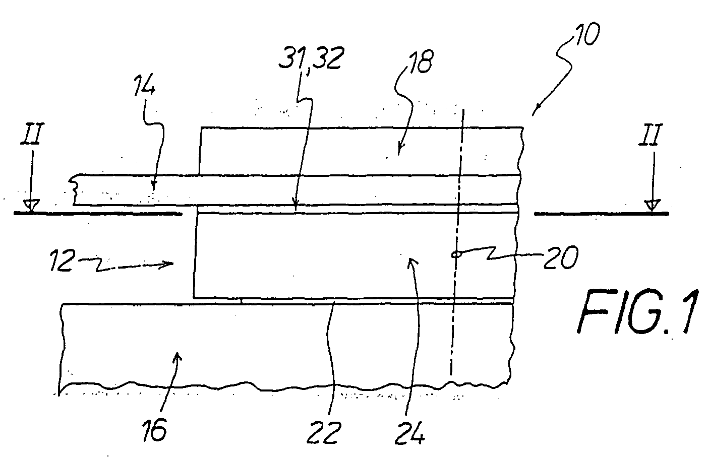
Es wird eine Schaltungsanordnung (10) mit einem Leistungsmodul (12) beschrieben, das mit einer Leiterplatte (14) kombiniert ist. Das Leistungsmodul (12) und die Leiterplatte (14) sind zwischen einem Kühlkörper (16) und einer Presseinrichtung (18) vorgesehen und miteinander durch Druckkontaktelemente (28) kontaktiert. Das Leistungsmodul (12) weist mindestens ein Modul-Plattenelement (22) und ein Gehäuse (24) auf, das mit Schächten (26) für die Druckkontaktelemente (28) ausgebildet ist. Die Schächte (26) münden aus der der Leiterplatte (14) zugewandten Grundfläche (30) des Gehäuses (24) an Mündungsöffnungen (40) aus. Die Grundfläche (30) des Gehäuses (24) ist um die Mündungsöffnungen (40) herum mit Öffnungs-Dichtrippen (42) ausgebildet. Ausserdem kann die Grundfläche (30) des Gehäuses (24) entlang ihres Aussenrandes (36) eine umlaufende Randdichtrippe (38) aufweisen. Ferner kann zwischen der Leiterplatte (14) und der Grundfläche (30) des Gehäuses (24) ein Abdichtflächenelement (32) vorgesehen sein.
Applications Claiming Priority (1)
| Application Number | Priority Date | Filing Date | Title |
|---|---|---|---|
| DE200610052619 DE102006052619B4 (en) | 2006-11-08 | 2006-11-08 | Circuit arrangement with a power module that is combined with a printed circuit board |
Publications (3)
| Publication Number | Publication Date |
|---|---|
| EP1921908A2 EP1921908A2 (en) | 2008-05-14 |
| EP1921908A3 true EP1921908A3 (en) | 2009-12-02 |
| EP1921908B1 EP1921908B1 (en) | 2012-08-01 |
Family
ID=39056377
Family Applications (1)
| Application Number | Title | Priority Date | Filing Date |
|---|---|---|---|
| EP20070021363 Active EP1921908B1 (en) | 2006-11-08 | 2007-11-02 | Circuit assembly with a power module that is combined with a circuit board |
Country Status (4)
| Country | Link |
|---|---|
| EP (1) | EP1921908B1 (en) |
| JP (1) | JP5183148B2 (en) |
| DE (1) | DE102006052619B4 (en) |
| DK (1) | DK1921908T3 (en) |
Families Citing this family (4)
| Publication number | Priority date | Publication date | Assignee | Title |
|---|---|---|---|---|
| JP6355994B2 (en) * | 2014-07-09 | 2018-07-11 | 株式会社ユーシン | Waterproof structure of control device |
| DE102014227024A1 (en) | 2014-12-30 | 2016-06-30 | Robert Bosch Gmbh | power device |
| DE102014227027A1 (en) | 2014-12-30 | 2016-06-30 | Robert Bosch Gmbh | Power semiconductor drive |
| EP3181284B1 (en) | 2015-12-17 | 2018-09-12 | Robert Bosch Gmbh | Frequency converter |
Citations (4)
| Publication number | Priority date | Publication date | Assignee | Title |
|---|---|---|---|---|
| DE19630173A1 (en) * | 1996-07-26 | 1998-01-29 | Semikron Elektronik Gmbh | Semiconductor power module for current rectifier |
| US6417747B1 (en) * | 2001-08-23 | 2002-07-09 | Raytheon Company | Low cost, large scale RF hybrid package for simple assembly onto mixed signal printed wiring boards |
| JP2005217075A (en) * | 2004-01-28 | 2005-08-11 | Denso Corp | Structure for fitting printed board |
| DE102005024900A1 (en) * | 2004-06-08 | 2006-01-05 | Fuji Electric Device Technology Co. Ltd. | Semiconductor device |
Family Cites Families (2)
| Publication number | Priority date | Publication date | Assignee | Title |
|---|---|---|---|---|
| JP3476142B2 (en) * | 2001-05-24 | 2003-12-10 | 日本電気株式会社 | Electronic device with dew condensation prevention structure |
| JP4764979B2 (en) * | 2004-06-08 | 2011-09-07 | 富士電機株式会社 | Semiconductor device |
-
2006
- 2006-11-08 DE DE200610052619 patent/DE102006052619B4/en active Active
-
2007
- 2007-10-25 JP JP2007277608A patent/JP5183148B2/en active Active
- 2007-11-02 DK DK07021363T patent/DK1921908T3/en active
- 2007-11-02 EP EP20070021363 patent/EP1921908B1/en active Active
Patent Citations (4)
| Publication number | Priority date | Publication date | Assignee | Title |
|---|---|---|---|---|
| DE19630173A1 (en) * | 1996-07-26 | 1998-01-29 | Semikron Elektronik Gmbh | Semiconductor power module for current rectifier |
| US6417747B1 (en) * | 2001-08-23 | 2002-07-09 | Raytheon Company | Low cost, large scale RF hybrid package for simple assembly onto mixed signal printed wiring boards |
| JP2005217075A (en) * | 2004-01-28 | 2005-08-11 | Denso Corp | Structure for fitting printed board |
| DE102005024900A1 (en) * | 2004-06-08 | 2006-01-05 | Fuji Electric Device Technology Co. Ltd. | Semiconductor device |
Also Published As
| Publication number | Publication date |
|---|---|
| DK1921908T3 (en) | 2012-10-22 |
| DE102006052619A1 (en) | 2008-05-15 |
| JP5183148B2 (en) | 2013-04-17 |
| JP2008124456A (en) | 2008-05-29 |
| DE102006052619B4 (en) | 2009-07-30 |
| EP1921908A2 (en) | 2008-05-14 |
| EP1921908B1 (en) | 2012-08-01 |
Similar Documents
| Publication | Publication Date | Title |
|---|---|---|
| EP1921910B1 (en) | Circuit with a power module that is combined with a circuit board | |
| DE102006008807B4 (en) | Arrangement with a power semiconductor module and a cooling component | |
| EP1843393A3 (en) | Pressure contact type power semiconductor module | |
| EP2273859A3 (en) | Use of a control module for a control unit built into an automatic gearbox | |
| DE102014016636A1 (en) | SENSOR | |
| EP1921908A3 (en) | Circuit assembly with a power module that is combined with a circuit board | |
| EP2334161A3 (en) | Control unit | |
| DE102005038466A1 (en) | Sensor arrangement for temperature measurement | |
| EP2261719A3 (en) | sample chamber and method of fabrication | |
| WO2005091690A1 (en) | Housing for an electronic circuit | |
| EP1976357B1 (en) | Housing for an electric switch and method for sealing such a housing | |
| DE19715592A1 (en) | Cooling device for an electronic module | |
| DE102008014457A1 (en) | Transmission control device for motor vehicle, has contact structures connected with each other by interface in mounted condition of two electrical components, where one component is provided with controller and other with sensor unit | |
| DE102016222630A1 (en) | Cooling device and method of manufacturing a cooling device | |
| EP1732131A3 (en) | Assembly apted to cool a group of power electronic components | |
| DE102011080178A1 (en) | Housing for electronic controller in motor car, has housing element pluggable on another housing element, and labyrinth seal formed between housing elements that are comprised of plastic and connectable by laser welding | |
| DE102008054384A1 (en) | Electrical circuit arrangement and method for producing an electrical circuit arrangement | |
| WO2013014005A1 (en) | Housing plug connector and housing having a housing plug connector | |
| DE102004007230B4 (en) | Housing with liquid-tight electrical feedthrough | |
| EP1865750A3 (en) | SMD battery contact module | |
| DE10308612B3 (en) | Electrical connection through a partition | |
| EP2608254A3 (en) | Semiconductor power module or actuation module for same | |
| DE102019126082B4 (en) | Hydraulic actuator with means for fastening a pressure sensor without its own housing | |
| DE10246577A1 (en) | Circuit board with metal housing, e.g. for motor vehicle control circuit, has spring member for making contact between circuit board or power semiconductor device and metal housing for heat removal | |
| DE202011050152U1 (en) | LED bulb with a connection arrangement for a translucent cover |
Legal Events
| Date | Code | Title | Description |
|---|---|---|---|
| PUAI | Public reference made under article 153(3) epc to a published international application that has entered the european phase |
Free format text: ORIGINAL CODE: 0009012 |
|
| AK | Designated contracting states |
Kind code of ref document: A2 Designated state(s): AT BE BG CH CY CZ DE DK EE ES FI FR GB GR HU IE IS IT LI LT LU LV MC MT NL PL PT RO SE SI SK TR |
|
| AX | Request for extension of the european patent |
Extension state: AL BA HR MK RS |
|
| PUAL | Search report despatched |
Free format text: ORIGINAL CODE: 0009013 |
|
| AK | Designated contracting states |
Kind code of ref document: A3 Designated state(s): AT BE BG CH CY CZ DE DK EE ES FI FR GB GR HU IE IS IT LI LT LU LV MC MT NL PL PT RO SE SI SK TR |
|
| AX | Request for extension of the european patent |
Extension state: AL BA HR MK RS |
|
| 17P | Request for examination filed |
Effective date: 20091105 |
|
| 17Q | First examination report despatched |
Effective date: 20091211 |
|
| AKX | Designation fees paid |
Designated state(s): AT BE BG CH CY CZ DE DK EE ES FI FR GB GR HU IE IS IT LI LT LU LV MC MT NL PL PT RO SE SI SK TR |
|
| REG | Reference to a national code |
Ref country code: DE Ref legal event code: R079 Ref document number: 502007010290 Country of ref document: DE Free format text: PREVIOUS MAIN CLASS: H05K0007140000 Ipc: H05K0001110000 |
|
| GRAP | Despatch of communication of intention to grant a patent |
Free format text: ORIGINAL CODE: EPIDOSNIGR1 |
|
| RIC1 | Information provided on ipc code assigned before grant |
Ipc: H05K 7/14 20060101ALI20120420BHEP Ipc: H05K 1/11 20060101AFI20120420BHEP Ipc: H05K 3/32 20060101ALI20120420BHEP |
|
| GRAS | Grant fee paid |
Free format text: ORIGINAL CODE: EPIDOSNIGR3 |
|
| GRAA | (expected) grant |
Free format text: ORIGINAL CODE: 0009210 |
|
| AK | Designated contracting states |
Kind code of ref document: B1 Designated state(s): AT BE BG CH CY CZ DE DK EE ES FI FR GB GR HU IE IS IT LI LT LU LV MC MT NL PL PT RO SE SI SK TR |
|
| REG | Reference to a national code |
Ref country code: GB Ref legal event code: FG4D Free format text: NOT ENGLISH |
|
| REG | Reference to a national code |
Ref country code: CH Ref legal event code: EP Ref country code: AT Ref legal event code: REF Ref document number: 569229 Country of ref document: AT Kind code of ref document: T Effective date: 20120815 |
|
| REG | Reference to a national code |
Ref country code: IE Ref legal event code: FG4D Free format text: LANGUAGE OF EP DOCUMENT: GERMAN |
|
| REG | Reference to a national code |
Ref country code: DE Ref legal event code: R096 Ref document number: 502007010290 Country of ref document: DE Effective date: 20120927 |
|
| REG | Reference to a national code |
Ref country code: DK Ref legal event code: T3 |
|
| REG | Reference to a national code |
Ref country code: NL Ref legal event code: VDEP Effective date: 20120801 |
|
| REG | Reference to a national code |
Ref country code: SK Ref legal event code: T3 Ref document number: E 12746 Country of ref document: SK |
|
| REG | Reference to a national code |
Ref country code: LT Ref legal event code: MG4D Effective date: 20120801 |
|
| PG25 | Lapsed in a contracting state [announced via postgrant information from national office to epo] |
Ref country code: LT Free format text: LAPSE BECAUSE OF FAILURE TO SUBMIT A TRANSLATION OF THE DESCRIPTION OR TO PAY THE FEE WITHIN THE PRESCRIBED TIME-LIMIT Effective date: 20120801 Ref country code: IS Free format text: LAPSE BECAUSE OF FAILURE TO SUBMIT A TRANSLATION OF THE DESCRIPTION OR TO PAY THE FEE WITHIN THE PRESCRIBED TIME-LIMIT Effective date: 20121201 Ref country code: FI Free format text: LAPSE BECAUSE OF FAILURE TO SUBMIT A TRANSLATION OF THE DESCRIPTION OR TO PAY THE FEE WITHIN THE PRESCRIBED TIME-LIMIT Effective date: 20120801 Ref country code: CY Free format text: LAPSE BECAUSE OF FAILURE TO SUBMIT A TRANSLATION OF THE DESCRIPTION OR TO PAY THE FEE WITHIN THE PRESCRIBED TIME-LIMIT Effective date: 20120801 |
|
| PG25 | Lapsed in a contracting state [announced via postgrant information from national office to epo] |
Ref country code: SI Free format text: LAPSE BECAUSE OF FAILURE TO SUBMIT A TRANSLATION OF THE DESCRIPTION OR TO PAY THE FEE WITHIN THE PRESCRIBED TIME-LIMIT Effective date: 20120801 Ref country code: GR Free format text: LAPSE BECAUSE OF FAILURE TO SUBMIT A TRANSLATION OF THE DESCRIPTION OR TO PAY THE FEE WITHIN THE PRESCRIBED TIME-LIMIT Effective date: 20121102 Ref country code: PT Free format text: LAPSE BECAUSE OF FAILURE TO SUBMIT A TRANSLATION OF THE DESCRIPTION OR TO PAY THE FEE WITHIN THE PRESCRIBED TIME-LIMIT Effective date: 20121203 Ref country code: PL Free format text: LAPSE BECAUSE OF FAILURE TO SUBMIT A TRANSLATION OF THE DESCRIPTION OR TO PAY THE FEE WITHIN THE PRESCRIBED TIME-LIMIT Effective date: 20120801 Ref country code: SE Free format text: LAPSE BECAUSE OF FAILURE TO SUBMIT A TRANSLATION OF THE DESCRIPTION OR TO PAY THE FEE WITHIN THE PRESCRIBED TIME-LIMIT Effective date: 20120801 Ref country code: LV Free format text: LAPSE BECAUSE OF FAILURE TO SUBMIT A TRANSLATION OF THE DESCRIPTION OR TO PAY THE FEE WITHIN THE PRESCRIBED TIME-LIMIT Effective date: 20120801 |
|
| PG25 | Lapsed in a contracting state [announced via postgrant information from national office to epo] |
Ref country code: NL Free format text: LAPSE BECAUSE OF FAILURE TO SUBMIT A TRANSLATION OF THE DESCRIPTION OR TO PAY THE FEE WITHIN THE PRESCRIBED TIME-LIMIT Effective date: 20120801 |
|
| PG25 | Lapsed in a contracting state [announced via postgrant information from national office to epo] |
Ref country code: EE Free format text: LAPSE BECAUSE OF FAILURE TO SUBMIT A TRANSLATION OF THE DESCRIPTION OR TO PAY THE FEE WITHIN THE PRESCRIBED TIME-LIMIT Effective date: 20120801 Ref country code: CZ Free format text: LAPSE BECAUSE OF FAILURE TO SUBMIT A TRANSLATION OF THE DESCRIPTION OR TO PAY THE FEE WITHIN THE PRESCRIBED TIME-LIMIT Effective date: 20120801 Ref country code: RO Free format text: LAPSE BECAUSE OF FAILURE TO SUBMIT A TRANSLATION OF THE DESCRIPTION OR TO PAY THE FEE WITHIN THE PRESCRIBED TIME-LIMIT Effective date: 20120801 Ref country code: ES Free format text: LAPSE BECAUSE OF FAILURE TO SUBMIT A TRANSLATION OF THE DESCRIPTION OR TO PAY THE FEE WITHIN THE PRESCRIBED TIME-LIMIT Effective date: 20121112 |
|
| BERE | Be: lapsed |
Owner name: SEMIKRON ELEKTRONIK G.M.B.H. & CO. KG Effective date: 20121130 |
|
| PG25 | Lapsed in a contracting state [announced via postgrant information from national office to epo] |
Ref country code: IT Free format text: LAPSE BECAUSE OF FAILURE TO SUBMIT A TRANSLATION OF THE DESCRIPTION OR TO PAY THE FEE WITHIN THE PRESCRIBED TIME-LIMIT Effective date: 20120801 |
|
| PLBE | No opposition filed within time limit |
Free format text: ORIGINAL CODE: 0009261 |
|
| STAA | Information on the status of an ep patent application or granted ep patent |
Free format text: STATUS: NO OPPOSITION FILED WITHIN TIME LIMIT |
|
| REG | Reference to a national code |
Ref country code: CH Ref legal event code: PL |
|
| 26N | No opposition filed |
Effective date: 20130503 |
|
| PG25 | Lapsed in a contracting state [announced via postgrant information from national office to epo] |
Ref country code: CH Free format text: LAPSE BECAUSE OF NON-PAYMENT OF DUE FEES Effective date: 20121130 Ref country code: BG Free format text: LAPSE BECAUSE OF FAILURE TO SUBMIT A TRANSLATION OF THE DESCRIPTION OR TO PAY THE FEE WITHIN THE PRESCRIBED TIME-LIMIT Effective date: 20121101 Ref country code: LI Free format text: LAPSE BECAUSE OF NON-PAYMENT OF DUE FEES Effective date: 20121130 |
|
| REG | Reference to a national code |
Ref country code: IE Ref legal event code: MM4A |
|
| REG | Reference to a national code |
Ref country code: DE Ref legal event code: R097 Ref document number: 502007010290 Country of ref document: DE Effective date: 20130503 |
|
| PG25 | Lapsed in a contracting state [announced via postgrant information from national office to epo] |
Ref country code: BE Free format text: LAPSE BECAUSE OF NON-PAYMENT OF DUE FEES Effective date: 20121130 |
|
| PG25 | Lapsed in a contracting state [announced via postgrant information from national office to epo] |
Ref country code: IE Free format text: LAPSE BECAUSE OF NON-PAYMENT OF DUE FEES Effective date: 20121102 |
|
| PG25 | Lapsed in a contracting state [announced via postgrant information from national office to epo] |
Ref country code: MT Free format text: LAPSE BECAUSE OF FAILURE TO SUBMIT A TRANSLATION OF THE DESCRIPTION OR TO PAY THE FEE WITHIN THE PRESCRIBED TIME-LIMIT Effective date: 20120801 |
|
| REG | Reference to a national code |
Ref country code: AT Ref legal event code: MM01 Ref document number: 569229 Country of ref document: AT Kind code of ref document: T Effective date: 20121130 |
|
| PG25 | Lapsed in a contracting state [announced via postgrant information from national office to epo] |
Ref country code: AT Free format text: LAPSE BECAUSE OF NON-PAYMENT OF DUE FEES Effective date: 20121130 |
|
| PG25 | Lapsed in a contracting state [announced via postgrant information from national office to epo] |
Ref country code: MC Free format text: LAPSE BECAUSE OF NON-PAYMENT OF DUE FEES Effective date: 20121130 Ref country code: TR Free format text: LAPSE BECAUSE OF FAILURE TO SUBMIT A TRANSLATION OF THE DESCRIPTION OR TO PAY THE FEE WITHIN THE PRESCRIBED TIME-LIMIT Effective date: 20120801 |
|
| PG25 | Lapsed in a contracting state [announced via postgrant information from national office to epo] |
Ref country code: LU Free format text: LAPSE BECAUSE OF NON-PAYMENT OF DUE FEES Effective date: 20121102 |
|
| PG25 | Lapsed in a contracting state [announced via postgrant information from national office to epo] |
Ref country code: HU Free format text: LAPSE BECAUSE OF FAILURE TO SUBMIT A TRANSLATION OF THE DESCRIPTION OR TO PAY THE FEE WITHIN THE PRESCRIBED TIME-LIMIT Effective date: 20071102 |
|
| REG | Reference to a national code |
Ref country code: FR Ref legal event code: PLFP Year of fee payment: 9 |
|
| REG | Reference to a national code |
Ref country code: FR Ref legal event code: PLFP Year of fee payment: 10 |
|
| PGFP | Annual fee paid to national office [announced via postgrant information from national office to epo] |
Ref country code: DK Payment date: 20161124 Year of fee payment: 10 Ref country code: SK Payment date: 20161026 Year of fee payment: 10 |
|
| REG | Reference to a national code |
Ref country code: FR Ref legal event code: PLFP Year of fee payment: 11 |
|
| REG | Reference to a national code |
Ref country code: DK Ref legal event code: EBP Effective date: 20171130 |
|
| PG25 | Lapsed in a contracting state [announced via postgrant information from national office to epo] |
Ref country code: SK Free format text: LAPSE BECAUSE OF NON-PAYMENT OF DUE FEES Effective date: 20171102 |
|
| REG | Reference to a national code |
Ref country code: SK Ref legal event code: MM4A Ref document number: E 12746 Country of ref document: SK Effective date: 20171102 |
|
| PG25 | Lapsed in a contracting state [announced via postgrant information from national office to epo] |
Ref country code: DK Free format text: LAPSE BECAUSE OF NON-PAYMENT OF DUE FEES Effective date: 20171130 |
|
| PGFP | Annual fee paid to national office [announced via postgrant information from national office to epo] |
Ref country code: GB Payment date: 20231123 Year of fee payment: 17 |
|
| PGFP | Annual fee paid to national office [announced via postgrant information from national office to epo] |
Ref country code: FR Payment date: 20231124 Year of fee payment: 17 Ref country code: DE Payment date: 20231130 Year of fee payment: 17 |