EP1912254B1 - Vertical-channel FinFET SONOS memory and manufacturing method thereof - Google Patents
Vertical-channel FinFET SONOS memory and manufacturing method thereof Download PDFInfo
- Publication number
- EP1912254B1 EP1912254B1 EP07118297.6A EP07118297A EP1912254B1 EP 1912254 B1 EP1912254 B1 EP 1912254B1 EP 07118297 A EP07118297 A EP 07118297A EP 1912254 B1 EP1912254 B1 EP 1912254B1
- Authority
- EP
- European Patent Office
- Prior art keywords
- layer
- nitride layer
- substrate
- patterned
- gate
- Prior art date
- Legal status (The legal status is an assumption and is not a legal conclusion. Google has not performed a legal analysis and makes no representation as to the accuracy of the status listed.)
- Active
Links
- 230000015654 memory Effects 0.000 title claims description 98
- 238000004519 manufacturing process Methods 0.000 title claims description 27
- 150000004767 nitrides Chemical class 0.000 claims description 82
- 239000000758 substrate Substances 0.000 claims description 43
- 238000000034 method Methods 0.000 claims description 26
- 239000000463 material Substances 0.000 claims description 20
- 229910052581 Si3N4 Inorganic materials 0.000 claims description 18
- HQVNEWCFYHHQES-UHFFFAOYSA-N silicon nitride Chemical compound N12[Si]34N5[Si]62N3[Si]51N64 HQVNEWCFYHHQES-UHFFFAOYSA-N 0.000 claims description 18
- VYPSYNLAJGMNEJ-UHFFFAOYSA-N Silicium dioxide Chemical compound O=[Si]=O VYPSYNLAJGMNEJ-UHFFFAOYSA-N 0.000 claims description 15
- 238000003860 storage Methods 0.000 claims description 13
- TWNQGVIAIRXVLR-UHFFFAOYSA-N oxo(oxoalumanyloxy)alumane Chemical compound O=[Al]O[Al]=O TWNQGVIAIRXVLR-UHFFFAOYSA-N 0.000 claims description 9
- 238000005530 etching Methods 0.000 claims description 8
- 150000002500 ions Chemical class 0.000 claims description 8
- 235000012239 silicon dioxide Nutrition 0.000 claims description 6
- 239000000377 silicon dioxide Substances 0.000 claims description 6
- 239000012212 insulator Substances 0.000 claims description 5
- NBIIXXVUZAFLBC-UHFFFAOYSA-N phosphoric acid Substances OP(O)(O)=O NBIIXXVUZAFLBC-UHFFFAOYSA-N 0.000 claims description 5
- 229910000147 aluminium phosphate Inorganic materials 0.000 claims description 4
- 229960004838 phosphoric acid Drugs 0.000 claims description 4
- 229910021420 polycrystalline silicon Inorganic materials 0.000 claims description 4
- 229920005591 polysilicon Polymers 0.000 claims description 4
- 229910052710 silicon Inorganic materials 0.000 claims description 4
- 239000010703 silicon Substances 0.000 claims description 4
- 238000009966 trimming Methods 0.000 claims description 4
- XUIMIQQOPSSXEZ-UHFFFAOYSA-N Silicon Chemical compound [Si] XUIMIQQOPSSXEZ-UHFFFAOYSA-N 0.000 claims description 3
- 229910052751 metal Inorganic materials 0.000 claims description 2
- 239000002184 metal Substances 0.000 claims description 2
- 150000002736 metal compounds Chemical class 0.000 claims description 2
- 108091006146 Channels Proteins 0.000 description 125
- 230000004888 barrier function Effects 0.000 description 12
- 238000011017 operating method Methods 0.000 description 10
- 239000004065 semiconductor Substances 0.000 description 9
- SEOYNUHKXVGWFU-UHFFFAOYSA-N mu-oxidobis(oxidonitrogen) Chemical group O=NON=O SEOYNUHKXVGWFU-UHFFFAOYSA-N 0.000 description 5
- 230000008569 process Effects 0.000 description 5
- 230000005641 tunneling Effects 0.000 description 5
- 230000015572 biosynthetic process Effects 0.000 description 4
- 230000000694 effects Effects 0.000 description 4
- 230000006870 function Effects 0.000 description 4
- 238000002347 injection Methods 0.000 description 4
- 239000007924 injection Substances 0.000 description 4
- 238000001020 plasma etching Methods 0.000 description 4
- KRHYYFGTRYWZRS-UHFFFAOYSA-N Fluorane Chemical compound F KRHYYFGTRYWZRS-UHFFFAOYSA-N 0.000 description 3
- 108090000699 N-Type Calcium Channels Proteins 0.000 description 3
- 102000004129 N-Type Calcium Channels Human genes 0.000 description 3
- 108010075750 P-Type Calcium Channels Proteins 0.000 description 3
- 238000000206 photolithography Methods 0.000 description 3
- 229910052814 silicon oxide Inorganic materials 0.000 description 3
- 239000004020 conductor Substances 0.000 description 2
- 239000002019 doping agent Substances 0.000 description 2
- 238000005516 engineering process Methods 0.000 description 2
- 239000002784 hot electron Substances 0.000 description 2
- 230000014759 maintenance of location Effects 0.000 description 2
- 238000001465 metallisation Methods 0.000 description 2
- 238000012986 modification Methods 0.000 description 2
- 230000004048 modification Effects 0.000 description 2
- 239000000047 product Substances 0.000 description 2
- 230000008859 change Effects 0.000 description 1
- 238000000151 deposition Methods 0.000 description 1
- 239000003989 dielectric material Substances 0.000 description 1
- 230000009977 dual effect Effects 0.000 description 1
- 230000005684 electric field Effects 0.000 description 1
- 230000005669 field effect Effects 0.000 description 1
- 239000013067 intermediate product Substances 0.000 description 1
- 238000002955 isolation Methods 0.000 description 1
- 238000011031 large-scale manufacturing process Methods 0.000 description 1
- QPJSUIGXIBEQAC-UHFFFAOYSA-N n-(2,4-dichloro-5-propan-2-yloxyphenyl)acetamide Chemical compound CC(C)OC1=CC(NC(C)=O)=C(Cl)C=C1Cl QPJSUIGXIBEQAC-UHFFFAOYSA-N 0.000 description 1
- 230000003647 oxidation Effects 0.000 description 1
- 238000007254 oxidation reaction Methods 0.000 description 1
- 238000012856 packing Methods 0.000 description 1
- 230000000149 penetrating effect Effects 0.000 description 1
- 230000009467 reduction Effects 0.000 description 1
- 238000011160 research Methods 0.000 description 1
Images


Classifications
-
- H—ELECTRICITY
- H10—SEMICONDUCTOR DEVICES; ELECTRIC SOLID-STATE DEVICES NOT OTHERWISE PROVIDED FOR
- H10B—ELECTRONIC MEMORY DEVICES
- H10B43/00—EEPROM devices comprising charge-trapping gate insulators
- H10B43/30—EEPROM devices comprising charge-trapping gate insulators characterised by the memory core region
-
- H—ELECTRICITY
- H01—ELECTRIC ELEMENTS
- H01L—SEMICONDUCTOR DEVICES NOT COVERED BY CLASS H10
- H01L29/00—Semiconductor devices adapted for rectifying, amplifying, oscillating or switching, or capacitors or resistors with at least one potential-jump barrier or surface barrier, e.g. PN junction depletion layer or carrier concentration layer; Details of semiconductor bodies or of electrodes thereof ; Multistep manufacturing processes therefor
- H01L29/66—Types of semiconductor device ; Multistep manufacturing processes therefor
- H01L29/66007—Multistep manufacturing processes
- H01L29/66075—Multistep manufacturing processes of devices having semiconductor bodies comprising group 14 or group 13/15 materials
- H01L29/66227—Multistep manufacturing processes of devices having semiconductor bodies comprising group 14 or group 13/15 materials the devices being controllable only by the electric current supplied or the electric potential applied, to an electrode which does not carry the current to be rectified, amplified or switched, e.g. three-terminal devices
- H01L29/66409—Unipolar field-effect transistors
- H01L29/66477—Unipolar field-effect transistors with an insulated gate, i.e. MISFET
- H01L29/66833—Unipolar field-effect transistors with an insulated gate, i.e. MISFET with a charge trapping gate insulator, e.g. MNOS transistors
-
- H—ELECTRICITY
- H01—ELECTRIC ELEMENTS
- H01L—SEMICONDUCTOR DEVICES NOT COVERED BY CLASS H10
- H01L29/00—Semiconductor devices adapted for rectifying, amplifying, oscillating or switching, or capacitors or resistors with at least one potential-jump barrier or surface barrier, e.g. PN junction depletion layer or carrier concentration layer; Details of semiconductor bodies or of electrodes thereof ; Multistep manufacturing processes therefor
- H01L29/40—Electrodes ; Multistep manufacturing processes therefor
- H01L29/43—Electrodes ; Multistep manufacturing processes therefor characterised by the materials of which they are formed
- H01L29/49—Metal-insulator-semiconductor electrodes, e.g. gates of MOSFET
- H01L29/51—Insulating materials associated therewith
- H01L29/511—Insulating materials associated therewith with a compositional variation, e.g. multilayer structures
- H01L29/513—Insulating materials associated therewith with a compositional variation, e.g. multilayer structures the variation being perpendicular to the channel plane
-
- H—ELECTRICITY
- H01—ELECTRIC ELEMENTS
- H01L—SEMICONDUCTOR DEVICES NOT COVERED BY CLASS H10
- H01L29/00—Semiconductor devices adapted for rectifying, amplifying, oscillating or switching, or capacitors or resistors with at least one potential-jump barrier or surface barrier, e.g. PN junction depletion layer or carrier concentration layer; Details of semiconductor bodies or of electrodes thereof ; Multistep manufacturing processes therefor
- H01L29/66—Types of semiconductor device ; Multistep manufacturing processes therefor
- H01L29/68—Types of semiconductor device ; Multistep manufacturing processes therefor controllable by only the electric current supplied, or only the electric potential applied, to an electrode which does not carry the current to be rectified, amplified or switched
- H01L29/76—Unipolar devices, e.g. field effect transistors
- H01L29/772—Field effect transistors
- H01L29/78—Field effect transistors with field effect produced by an insulated gate
- H01L29/792—Field effect transistors with field effect produced by an insulated gate with charge trapping gate insulator, e.g. MNOS-memory transistors
-
- H—ELECTRICITY
- H10—SEMICONDUCTOR DEVICES; ELECTRIC SOLID-STATE DEVICES NOT OTHERWISE PROVIDED FOR
- H10B—ELECTRONIC MEMORY DEVICES
- H10B69/00—Erasable-and-programmable ROM [EPROM] devices not provided for in groups H10B41/00 - H10B63/00, e.g. ultraviolet erasable-and-programmable ROM [UVEPROM] devices
-
- G—PHYSICS
- G11—INFORMATION STORAGE
- G11C—STATIC STORES
- G11C16/00—Erasable programmable read-only memories
- G11C16/02—Erasable programmable read-only memories electrically programmable
- G11C16/04—Erasable programmable read-only memories electrically programmable using variable threshold transistors, e.g. FAMOS
- G11C16/0466—Erasable programmable read-only memories electrically programmable using variable threshold transistors, e.g. FAMOS comprising cells with charge storage in an insulating layer, e.g. metal-nitride-oxide-silicon [MNOS], silicon-oxide-nitride-oxide-silicon [SONOS]
-
- H—ELECTRICITY
- H01—ELECTRIC ELEMENTS
- H01L—SEMICONDUCTOR DEVICES NOT COVERED BY CLASS H10
- H01L29/00—Semiconductor devices adapted for rectifying, amplifying, oscillating or switching, or capacitors or resistors with at least one potential-jump barrier or surface barrier, e.g. PN junction depletion layer or carrier concentration layer; Details of semiconductor bodies or of electrodes thereof ; Multistep manufacturing processes therefor
- H01L29/66—Types of semiconductor device ; Multistep manufacturing processes therefor
- H01L29/68—Types of semiconductor device ; Multistep manufacturing processes therefor controllable by only the electric current supplied, or only the electric potential applied, to an electrode which does not carry the current to be rectified, amplified or switched
- H01L29/76—Unipolar devices, e.g. field effect transistors
- H01L29/772—Field effect transistors
- H01L29/78—Field effect transistors with field effect produced by an insulated gate
- H01L29/785—Field effect transistors with field effect produced by an insulated gate having a channel with a horizontal current flow in a vertical sidewall of a semiconductor body, e.g. FinFET, MuGFET
Description
- The invention relates in general to a vertical channel memory and a manufacturing method thereof and an operating method using the same, and more particularly to a vertical channel memory with high scalability and a manufacturing method thereof and an operating method using the same.
- Along with the advance in the manufacturing technology of semiconductor, the resolution of current semiconductor elements has reached nano level. Take the memory for example, the length of the gate and the element pitch are further reduced. Despite the photolithography improves continuously, the manufactured planar transistor structure has reached the resolution limit of photolithography, the manufactured transistor element still has the problems of electrostatics discharge (ESD), leakage, reduction in electron mobility, and is apt to short channel effect and drain induced barrier lowering (DIBL) effect. Therefore, the double-gate vertical channel transistor and the tri-gate vertical channel transistor capable of providing higher packing density, better carrier transport and device scalability, such as fin field effect transistor (FinFET), have become transistor structures with great potential.
- The FinFET has vertical channel, and can form channels on two vertical surfaces and control the connection of current by double-gate or tri-gate, hence having better efficiency than conventional planar channel transistor.
- The manufacturing of FinFET elements with high resolution still requires expensive and advanced manufacturing process by photolithography or E-beam. However, the throughput of these advance manufacturing processes is difficult to increase and is disadvantageous to large-scale production. One of the present manufacturing methods is ecthing a channel first and then the line width of the channel is reduced by oxidation. However, the element formed according to such method has poor uniformity and the quality is difficult to control.
-
US 2006/0181925 A1 describes a nonvolatile memory cell arrangement. The nonvolatile memory cell arrangement comprises memory transistors, which are arranged in a plurality of rows and columns. A first source/drain terminal of each memory transistor of a first column is connected to an electrically conductive conductor track in a first metallization plane, and a first source/drain terminal of each memory transistor of a second column adjusted to the first column is connected to an electrically conductive conductor track in a second metallization plane. - Methods of forming non-volatile semiconductor memory devices using prominences and trenches and devices so formed are described in
US 2006/0141706 A1 . During the performance of the methods, a semiconductor substrate is pattern to form a depression and prominence. A floating gate is then formed so as to cover at least both sidewalls, and is further etched to form a trench for a device isolation self-aligned with the floating gate. - Moreover, the publication Falong Zhou et al: "VDNROM: A Novel Four-Bits-Per-Cell Vertical Channel Dual-Nitride-Trapping-Layer ROM for High Density Flash Memory Applications" (Solid-State Device Research Conference, 2006; ESSDERC 2006; Proceeding Of The 36th European, IEEE, PI, 1 September 2006 (2006-09-01), pages 226 - 229, XP031047034, ISBN: 978-1-4244-0301-1) describes a vertical channel nonvolatile memory cell with an oxide-nitride-oxide-nitride-oxide dielectrics stack. The fabrication process for such a VDNROM device is also described within the publication.
- Furthermore,
US 2005/0124099 A1 describes a self-aligned source/drain FinFET process flow. The self-aligned FinFET is fabricated by defining a set of fins in a semiconductor wafer, depositing gate material over the fins, defining a gate hardmask and etching the gate material outside the hardmask to form the gate. A conformal layer of insulator is further deposited over the gate and the fins, before the insulator is anisotropically etched until the insulator over the fins is removed down to the substrate. - In addition,
US 2005/0226047 A1 describes a semiconductor device with at least one electrically rewritable semiconductor memory cell provides by a vertical channel memory.US 2005/0226047A1 also describes a method of manufacture for producing said semiconductor device. - The invention provides a vertical channel memory according to
claim 1, and a method of manufacturing a vertical channel memory according to claim 7.
The invention will become apparent from the following detailed description of the preferred but non-limiting embodiments. The following description is made with reference to the accompanying drawings. -
-
FIG. 1A is a top view of a vertical channel memory according to a first embodiment of the invention; -
FIG. 1B is a cross-sectional view along a cross-sectional line AA' ofFIG. 1A ; -
FIGs. 2A-2J illustrate the manufacturing process of the vertical channel memory according to the first embodiment of the invention; -
FIG. 3 is a flowchart illustrating the manufacturing steps of the vertical channel memory according to the first embodiment of the invention; -
FIG. 4A is a top view of a vertical channel memory according to a second embodiment not forming part of the invention; -
FIG. 4B is a cross-sectional view along a cross-sectional line BB' ofFIG. 4A ; -
FIGs. 5A-5J illustrate the manufacturing process of the vertical channel memory according to the second embodiment not forming part of the invention; -
FIG. 6 is a flowchart illustrating the manufacturing steps of the vertical channel memory according to the second embodiment not forming part of the invention; -
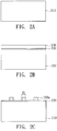
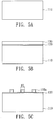
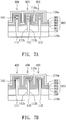
FIG. 7A is a sectional view of a first vertical channel memory according to a third embodiment of the invention; -
FIG. 7B is a sectional view of a second vertical channel memory not forming part of the invention; -
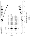
FIG. 8A compares the relationship curve of threshold voltage vs. programming time between the vertical channel memory of the third embodiment of the invention and the conventional vertical channel memory; -
FIG. 8B compares the relationship curve of threshold voltage vs. erase time between the vertical channel memory of the third embodiment of the invention and the conventional vertical channel memory; and -
FIG. 9 compares the relationship curve of threshold voltage vs. retention time between the BE-SONOS vertical channel memory and the conventional SONOS vertical channel memory. - Referring to
FIG. 1A and FIG. 1B. FIG. 1A is a top view of a vertical channel memory according to a first embodiment of the invention.FIG. 1B is a cross-sectional view along a cross-sectional line AA' ofFIG. 1A . As indicated inFIG. 1B , thevertical channel memory 100 includes asubstrate 110a, achannel 112 protruded from thesubstrate 110a and acap layer 140 disposed on thechannel 112. Thechannel 112 has atop surface 112a and twovertical surfaces 112b. Thechannel 112 substantially has the same width as that of thecap layer 140. In the present embodiment of the invention, thecap layer 140, an intermediate product during the manufacturing process, includes a silicon dioxide (SiO2) layer and a silicon nitride (SiN) layer, wherein the silicon nitride layer is positioned on the silicon dioxide layer. Thecap layer 140 with appropriate thickness avoids the electron penetrating from the gate, therefore avails the formation of a dual channel vertical memory, makes the electrical field of thechannel 112 more uniform, and prevents thechannel 112 from generating leakage current. A multilayer structure, that is, an oxide-nitride-oxide (ONO)layer 160 in the present embodiment of the invention is disposed on twovertical surfaces 112b of thechannel 112 and includes anoxide layer 161, anitride layer 162 and anoxide layer 163, wherein theoxide layer 161 and theoxide layer 163 contain thenitride layer 162. TheONO layer 160 is disposed on thecap layer 140 as a charge storage structure, and straddles over the fin structure of thechannel 112. Theoxide layer 161 and theoxide layer 163 are made from silicon oxide. Thenitride layer 162 is a charge trapping layer, and is made from silicon nitride in the present embodiment of the invention. Furthermore, thenitride layer 162 can also be made from aluminum oxide (Al2O3) or other materials with a high dielectric constant. TheONO layer 160 is a charge storage structure for enabling thevertical channel memory 100 to have the function of programming and erasing data. Thegate 170a straddles thenitride layer 162, that is, thegate 170a is positioned on the fin structure of thechannel 112. Due to the two vertical surfaces of thechannel 112 capable of respectively controlling the connection of the current by thegate 170a, thevertical channel memory 100 is called the double-gate structure. Thegate 170a can be made from N+ polysilicon, P+ polysilicon, metal compound or metal. As indicated inFIG. 1A , thefirst terminal 192 and thesecond terminal 194 are respectively positioned at the two sides of thechannel 112 relative to thegate 170a. The present embodiment of the invention is exemplified by an NAND array memory structure, thefirst terminal 192 and thesecond terminal 194 are respectively a source and a drain or a drain and a source, and the source and the drain between any twovertical channel memories 100 are a common source and a common drain. The line width of thechannel 112 approximately ranges between 10 nm-60 nm. - Besides, as indicated in
FIG. 1B , thevertical channel memory 100 further includes athick oxide layer 150 positioned on thesubstrate 110a. In the present embodiment of the invention, thethick oxide layer 150 is made from silicon oxide. Thethick oxide layer 150 avoids thesubstrate 110a being electrically connected, hence generating leakage current. - The application of the present embodiment of the invention is exemplified below by the manufacturing process of the NAND. Referring to
FIGs. 2A-2J , perspectives illustrating the manufacturing process of the vertical channel memory according to the first embodiment of the invention are shown. Also referring toFIG. 3 , a flowchart illustrating the manufacturing steps of the vertical channel memory according to the first embodiment of the invention is shown. - First, referring to
FIG. 2A . As indicated instep 301, asubstrate 110 is provided. Examples of thesubstrate 110 include bulk silicon substrate or silicon on insulator (SOI) substrate. - Next, referring to
FIG. 2B . As indicated instep 302, afirst nitride layer 130 is formed on thesubstrate 110. In the present embodiment of the invention, thefirst nitride layer 130 is made from silicon nitride, and preferably, apad oxide layer 120 formed between thesubstrate 110 and thefirst nitride layer 130 is made from silicon nitride. Furthermore, a transistor with N-type channel is formed in the present embodiment of the invention, so P-type ions can be implanted to thesubstrate 100 in the current step, such that thesubstrate 100 has better quality when forming a channel in subsequent process. However, the present embodiment of the invention is not limited thereto. If the transistor is designed to have P-type channel, then N-type ions are implanted to thesubstrate 100. - Then, referring to
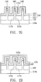
FIG. 2C . As indicated instep 303, thefirst nitride layer 130 is etched to form a firstpatterned nitride layer 130a. In the present embodiment of the invention, thefirst nitride layer 130 is made from silicon nitride. Step 303 includes the following substeps. First, a first patterned photo-resist layer (not illustrated) is formed on thefirst nitride layer 130. Next, thefirst nitride layer 130 is etched to form the firstpatterned nitride layer 130a. Then, the first patterned photo-resist layer is removed. The resulted first patternednitride layer 130a has a pattern with line width D1. The current step can adopt the reactive ion etching (RIE) method. - Next, referring to
FIG. 2D . As indicated instep 304, the firstpatterned nitride layer 130a is trimmed to form a secondpatterned nitride layer 130b. The resulted second patternednitride layer 130b after trimming has a pattern with line width D2. The line width D2 approximately ranges between 10 nm-60 nm. Hot-phosphoric-acid, having excellent etching selectivity with respect to silicon nitride and silicon oxide, is used to trim the firstpatterned nitride layer 130a in the current step. - Then, referring to
FIG. 2E . As indicated instep 305, thesubstrate 110 is etched to form asubstrate 110a, and achannel 112 protruded from thesubstrate 110a is formed on thesubstrate 110a. Thechannel 112 has atop surface 112a and twovertical surfaces 112b. In the present embodiment of the invention, preferably after thepad oxide layer 120 is etched to formpad oxide layer 120a according to the RIE method, thesubstrate 110 is subsequently etched to form achannel 112. Meanwhile, thepad oxide layer 120a and the secondpatterned nitride layer 130b as a whole is called acap layer 140. - Next, referring to
FIG. 2F . Athick oxide layer 150 contacting twovertical surfaces 112b of thechannel 112 is formed. In the current step, thethick oxide layer 150 is deposited by high density plasma (HDP). Thethick oxide layer 150 restricts the height of the fin channel, such that the current can only flows through the portion of thechannel 112 above thethick oxide layer 150. - Then, referring to
FIG. 2G . As indicated instep 306, an oxide-nitride-oxide (ONO)layer 160 is formed. TheONO layer 160 is disposed on thecap layer 140 and twovertical surfaces 112b of thechannel 112 and thethick oxide layer 150. TheONO layer 160 includes anoxide layer 161, anitride layer 162 and anoxide layer 163. In the present embodiment of the invention, thenitride layer 162 uses silicon nitride as the charge trapping layer such that a charge storage structure is formed. However, thenitride layer 162 can also use aluminum oxide (Al2O3) or other materials with high dielectric constant as the charge trapping layer. - Next, referring to
FIG. 2H . As indicated instep 307, agate material layer 170 is formed on theONO layer 160. - Then, referring to
FIG. 2I . As indicated instep 308, thegate material layer 170 is etched to form at least a gate straddling over the fin structure of thechannel 112. Beforestep 308 is performed, preferably the following substeps are performed. First, a second nitride layer (not illustrated) is formed on thegate material layer 170. In the present embodiment of the invention, the second nitride layer is made from silicon nitride. Next, a second patterned photo-resist layer (not illustrated) is formed on the second nitride layer. Then, the second nitride layer is etched to form a thirdpatterned nitride layer 180. Next, the second patterned photo-resist layer is removed. Then, the thirdpatterned nitride layer 180 is trimmed to form a fourthpatterned nitride layer 180a. Then, referring toFIG. 2J . Thegate material layer 170 is etched according to the pattern of the fourthpatterned nitride layer 180a to form thegate 170a. After thegate 170a is formed, preferably the fourthpatterned nitride layer 180a is removed. Thus, a gate structure whose line width approximately ranging between 10 nm-60 nm is formed. - Next, as indicated in
step 309, ions are implanted to the two sides of thechannel 112 relative to thegate 170a to form thefirst terminal 192 and thesecond terminal 194. Up to now, the main structure of the NAND memory array havingvertical channel memory 100 is completed. The present embodiment of the invention is exemplified by the formation of a transistor with N-type channel, so N-type dopants are implanted in the current step. If the transistor is designed to have P-type channel, then P-type dopants are implanted. - Referring to
FIG. 4A and FIG. 4B. FIG. 4A is a top view of a vertical channel memory according to a second embodiment not forming part of the invention.FIG. 4B is a cross-sectional view along a cross-sectional line BB' ofFIG. 4A . Thevertical channel memory 200 of the present embodiment differs with thevertical channel memory 100 of the first embodiment in that thecap layer 140 is removed. As for other elements common to thevertical channel memory 100, the same numeric designations are used and the functions are not repeated here. - As the
oxide layer 140 is removed, the top surface of thechannel 112 capable of controlling the connection of current by thegate 170a is called a tri-gate structure. - The application of the present embodiment is exemplified below by the manufacturing process of the NAND memory array structure. Referring to
FIGS. 5A-5J , perspectives illustrating the manufacturing process of the vertical channel memory according to the second embodiment are shown. Also referring toFIG. 6 , a flowchart illustrating the manufacturing steps of the vertical channel memory according to the second embodiment. - First, referring to
FIG. 5A . As indicated instep 601, asubstrate 110 is provided. - Next, referring to
FIG. 5B . As indicated instep 602, afirst nitride layer 130 is formed on thesubstrate 110. In the present embodiment, preferably apad oxide layer 120 is formed between thesubstrate 110 and thefirst nitride layer 130. Furthermore, a transistor with N-type channel is formed in the present embodiment, so P-type ions are implanted to thesubstrate 110, such that thesubstrate 110 has better quality when forming a channel in subsequent process. However, the present embodiment is not limited thereto. If the transistor is designed to have P-type channel, then N-type ions are implanted to thesubstrate 100. - Then, referring to
FIG. 5C . As indicated instep 603, thefirst nitride layer 130 is etched to form a firstpatterned nitride layer 130a. Step 603 includes the following substeps. The first patterned photo-resist layer (not illustrated) is formed on thefirst nitride layer 130. Next, thefirst nitride layer 130 is etched to form the firstpatterned nitride layer 130a. Then, the first patterned photo-resist layer is removed. The resulted first patternednitride layer 130a has a pattern with line width D1. - Next, referring to
FIG. 5D . As indicated instep 604, the firstpatterned nitride layer 130a is trimmed to form a secondpatterned nitride layer 130b. The resulted second patternednitride layer 130b after trimming has a pattern with line width D2 approximately ranging between 10 nm-60 nm. - Then, Referring to
FIG. 5E . As indicated instep 605, thesubstrate 110 is etched to form asubstrate 110a, and achannel 112 protruded from thesubstrate 110a is formed on thesubstrate 110a. Thechannel 112 has atop surface 112a and twovertical surfaces 112b. In the present embodiment, preferably after thepad oxide layer 120 is etched to formpad oxide layer 120a according to the RIE method, thesubstrate 110 is subsequently etched to form achannel 112. Meanwhile, thepad oxide layer 120a and the secondpatterned nitride layer 130b as a whole is called acap layer 140. - Next, referring to
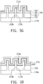
FIG. 5F . Athick oxide layer 150 avoids the substrate surface being electrically connected, hence generating leakage current. As indicated instep 606, on thechannel 112, thecap layer 140 formed by the secondpatterned nitride layer 130b andpad oxide layer 120a is removed. The current step can be achieved by hot-phosphoric-acid (H3PO4). Meanwhile, preferably thepad oxide layer 120a is removed. The current step can be achieved by hydrofluoric acid (HF). The step of removing the secondpatterned nitride layer 130b and thepad oxide layer 120a can be performed either before or after the formation of thethick oxide layer 150. - Then, referring to
FIG. 5G . As indicated instep 607, an oxide-nitride-oxide (ONO)layer 160 is formed. TheONO layer 160 is disposed on twovertical surfaces 112b of thechannel 112 and thethick oxide layer 150. TheONO layer 160 includes anoxide layer 161, anitride layer 162 and anoxide layer 163. In the present embodiment, thenitride layer 162 uses silicon nitride as the charge trapping layer. However, thenitride layer 162 can also use aluminum oxide (Al2O3) or other materials with high dielectric constant as the charge trapping layer such that the charge storage structure is formed. - Next, referring to
FIG. 5H . As indicated instep 608, agate material layer 170 is formed on theONO layer 160. - Then, referring to
FIG. 5I . As indicated instep 609, thegate material layer 170 is etched to form at least agate 170a positioned on twovertical surfaces 112b and thetop surface 112a of thechannel 112. Preferably, the following steps are performed beforestep 609. First, a second nitride layer (not illustrated) is formed on thegate material layer 170. Next, a second patterned photo-resist layer (not illustrated) is formed on the second nitride layer. Then, the second nitride layer is etched to form a thirdpatterned nitride layer 180. Next, the second patterned photo-resist layer is removed. Then, the thirdpatterned nitride layer 180 is trimmed to form a fourthpatterned nitride layer 180a. Then, referring toFIG. 2J , thegate material layer 170 is etched according to the pattern of the fourthpatterned nitride layer 180a to form thegate 170a. Preferably the step of removing the fourthpatterned nitride layer 180a is included after thegate 170a is formed. - Next, as indicated in
step 610, ions are implanted to two sides of thechannel 112 relative to thegate 170a to form thefirst terminal 192 and thesecond terminal 194. Up to now, the main structure of the NAND memory array havingvertical channel memory 200 is completed. - Referring to
FIG. 7A and FIG. 7B, FIG. 7A is a sectional view of a first vertical channel memory according to a third embodiment of the invention.FIG. 7B is a sectional view of a second vertical channel memory not forming part of the invention. Thevertical channel memories vertical channel memory 100 of the first embodiment and thevertical channel memory 200 of the second embodiment in that theONO layer 160 is replaced by an multilayer structure including at least four layers, that is a barrier layer disposed on thechannel 112, and a tunneling layer, a charge trapping layer and another barrier layer stacking sequently. In the third embodiment, the multilayer structure has five layers, that is anONONO layer 360 having a first barrier layer disposed on thechannel 112, and a tunneling layer, a second barirer layer, a charge trapping layer and a third barrier layer stacking sequently, hence forming a memory with band gap engineered silicon-oxide-nitride-oxide-silicon (BE-SONOS) structure. As for other elements of thevertical channel memories vertical channel memory 100 andvertical channel memory 200, the same numeric designations are used and functions thereof are not repeated here. - The
ONONO layer 360 includes anoxide layer 361 as the first barrier layer, anitride layer 362 as the tunneling layer, anoxide layer 363 as the second barrier layer, anitride layer 364 as the charge trapping layer and anoxide layer 365 as the third barrier layer. That is, theoxide layer 161 of theONO layer 160 is replaced by theoxide layer 301, thenitride layer 362 and theoxide layer 363, hence resulting in even better operating characteristics. Besides, thenitride layer 362 can be replaced by a polysilcon layer as the tunneling layer. Thenitride layer 364 of theONONO layer 360 can also use aluminum oxide or other materials with high dielectric constant as the charge trapping layer. The thickness of the first barrier layer, likeoxide layer 361, is less than 20 angstrom (Å). The thickness of the first barrier layer preferably ranges between 5 Å-20 Å. Furthermore, the thickness of the first barrier layer is less than 15 Å. The thickness of the tunneling layer, likenitride layer 362, is less than 20 Å, and preferably ranges between 10 Å-20 Å. The thickness of the second barrier layer, likeoxide layer 363, is less than 20 Å, and preferably ranges between 15 Å -20 -
FIG. 8A compares the relationship curve of threshold voltage vs. programming time between the vertical channel memory of the third embodiment of the invention and the conventional vertical channel memory.FIG. 8B compares the relationship curve of threshold voltage vs. erase time between the vertical channel memory of the third embodiment of the invention and the conventional vertical channel memory. As indicated inFIG. 8A , when the same gate voltage VG is applied, the vertical channel memory with BE-SONOS structure of the present embodiment of the invention increases the threshold voltage faster than the vertical channel memory of conventional SONOS structure, hence resulting in much faster programming speed. As indicated inFIG. 8B , when the same gate voltage VG is applied, the vertical channel memory with BE-SONOS structure of the present embodiment of the invention reduces the threshold voltage much faster than the vertical channel memory with conventional SONOS structure, hence resulting in much faster erase speed. - As indicated in
FIG. 8B , the vertical channel memory with BE-SONOS structure can be erased up to negative threshold voltage, hence largely increasing the range of operating window, and achieving the function of a multi-level cell (MLC) memory. When the BE-SONOS structure is used in an NAND memory array, as the threshold voltage can be negative during erasing, the channel can be inverted and turned on without applying extra bias to the gate, such that the operating procedures are simplified and power consumption is reduced. -
FIG. 9 compares the relationship curve of threshold voltage vs. retention time between the BE-SONOS vertical channel memory and the conventional SONOS vertical channel memory. As illustrated inFIG. 9 , at 150°C ambient temperature, the change of the threshold voltage of the BE-SONOS vertical channel memory and that of the conventional SONOS vertical channel memory under different programming-erasing cycles are shown. It can be seen that BE-SONOS vertical channel memory can maintain more stable threshold voltage, and especially perform excellent at high threshold voltage status. - Likewise, let the manufacturing process of the NAND memory array structure be taken for example. The manufacturing process of the
vertical channel memories channel transistor structures ONO layer 160 as instep 306 andstep 607. In the present embodiment of the invention, theONONO layer 360 is formed on the twovertical surfaces 112b of thechannel 112 and thethick oxide layer 150. Other processes common to the first embodiment and the second embodiment are not repeated here. - As for the operating method of the vertical channel memory with BE-SONOS structure, the positive Fowler-Nordiem (+FN) operating method is adopted in programming data, that is, a first bias is applied to the
gate 170a for programming thevertical channel memory gate 170a for erasing thevertical channel memory oxide layer 361 close to the channel being damaged, and increasing product reliability. - Moreover, the vertical channel memory with BE-SONOS structure is programmed according to channel hot electron injection (CHEI) method, that is, the
vertical channel memory gate 170a, and a third bias whose polarity is the same as the first bias is applied to thefirst terminal 192 or thesecond terminal 194, wherein the first bias is larger than 7V, and the third bias is larger than 3.2V. Similarly, the vertical channel memory with BE-SONOS structure is erased according to the band-to-band hot hole (BTBHH) method, that is, thevertical channel memory gate 170a, and a fourth bias whose polarity is the same as the first bias is applied to thefirst terminal 192 or thesecond terminal 194, wherein the second bias is smaller than 0V, and the fourth bias is larger than 10.6V. As the nitride can trap the charge locally, the above operating method can achieve dual-bit memory by storing different bits in the portion of theONONO layer 360 close to the source or the drain. In the present embodiment of the invention, the vertical channel memory with BE-SONOS structure is programmed according to channel hot electron injection (CHEI) method, and the vertical channel memory with BE-SONOS structure is erased according to the band-to-band hot hole (BTBHH) method, however the invention is not limited thereto. The vertical channel memory can be programmed according to the hole injection method and erased according to the electron injection method. - According to the vertical channel memory and manufacturing method thereof and operating method using the same disclosed in the above embodiments of the invention, hot-phosphoric-acid is used to further reduce the line width of the pattern formed by nitride such that a vertical channel transistor structure whose channel width ranges between 10 nm-60 nm is manufactured without changing the pitch of the element formed by exposure. The invention effectively increases the driving current during programming or reading without incurring short channel effect or DIBL effect. The FinFET transistor formed thereby has small dimension, hence increasing memory density significantly. Therefore, without using an expensive exposure machine, a transistor structure having narrow channel can be manufactured according to the technology of the invention. The hard mask used in the invention adopts silicon nitride and resists the impact of ions better than conventional photo-resist layer, therefore the invention can etch and result in a uniform semiconductor element without increasing the thickness of the photo-resist layer. The vertical channel memory with BE-SONOS structure can locally trap the charge and can enlarge the range of the operating window to achieve an MLC memory. The operating method of +FN programming method and -FN erasing method have the advantages of lowering operating current, reducing power consumption, avoiding the bottom oxide layer close to the channel being damaged, and increasing product reliability.
- While the invention has been described by way of example and in terms of preferred embodiments, it is to be understood that the invention is not limited thereto. On the contrary, it is intended to cover various modifications and similar arrangements and procedures, and the scope of the appended claims therefore should be accorded the broadest interpretation so as to encompass all such modifications and similar arrangements and procedures.
Claims (11)
- A vertical channel memory (100, 300), being a FinFET structure, and comprising:a substrate (110a);a fin channel structure (112) protruded from the substrate (110a);a cap layer (140) deposited on a top surface of the fin channel structure (112), wherein the cap layer (140) comprises a silicon dioxide layer (120a) and a silicon nitride layer (130b), the silicon nitride layer (130b) is positioned on the silicon dioxide layer (120a), and the cap layer (140) and the fin channel structure (112) have the same line width (D2);a multilayer charge storage structure (160, 360) deposited on two vertical surfaces (112b) of the fin channel structure (112) and on the cap layer (140), wherein the multilayer charge storage structure (160, 360) directly contacts side surfaces of the silicon nitride layer (130b) and the silicon dioxide layer (120a) of the cap layer (140) and a top surface of the silicon nitride layer (130b), and the multilayer charge storage structure (160, 360) includes a charge trapping layer (162, 364);a gate (170a) straddling on the multilayer charge storage structure (160, 360) and positioned on the upper surface of the cap layer (140) and the two vertical surfaces (112b) of the fin channel structure (112); anda first terminal (192) and a second terminal (194) respectively positioned on the two sides of the fin channel structure (112) and relative to the gate (170a), whereina line width of the fin channel structure (112) ranges between 10 nm to 60 nm.
- The vertical channel memory (100, 300) according to claim 1, characterized in that it further comprises a thick oxide layer (150) positioned on the substrate (110a), wherein the thick oxide layer (150) contacting the two vertical surfaces (112b) of the fin channel structure (112).
- The vertical channel memory (100, 300) according to claim 1, characterized in that the material of the charge trapping layer (162, 364) is SiN,
aluminum oxide (Al2O3) or other high dielectric constant material. - The vertical channel memory (100, 300) according to claim 2, characterized in that the multilayer charge storage structure (160, 360) comprises a first oxide layer (161, 363) and a second oxide layer (163, 365), the first oxide layer (161, 363) is positioned between the charge trapping layer (162, 364) and the fin channel structure (112), and the second oxide layer (163, 365) is positioned between the charge trapping layer (162, 364) and the gate (170a).
- The vertical channel memory (100, 300) according to claim 1, characterized in that the substrate (110a) is a bulk silicon substrate or a silicon-on-insulator (SOI) substrate.
- The vertical channel memory (100, 300) according to claim 1,
characterized in that the material of the gate (170a) is N+ polysilicon, P+ polysilicon, metal compound or metal. - A method of manufacturing a vertical channel memory (100, 300) being a FinFET structure, comprising:(a) providing a substrate (110);(a1) forming a pad oxide layer (120) on the substrate (110);(b) forming a first nitride layer (130) on the pad oxide layer (120);(c) etching the first nitride layer (130) to form a first patterned nitride layer (130a);(d) trimming the first patterned nitride layer (130a) to form a second patterned nitride layer (130b), wherein a line width (D2) of the second patterned nitride layer (130b) ranges between 10 nm to 60nm;(d1) etching the pad oxide layer (120), wherein the second patterned nitride layer (130b) and the pad oxide layer (120a) form a cap layer (140);(e) etching the substrate (110) to form at least a fin channel structure (112) protruded from the substrate (110a), wherein a line width of the fin channel structure (112) ranges between 10 nm to 60 nm, and the cap layer (140) and the fin cannel structure (112) have the same width (D2);(f) forming a thick oxide layer (150) on top surface of the substrate (110a);(g) forming a multilayer charge storage structure (160, 360) on two vertical surfaces (112b) of the fin channel structure (112) and directly contacting side surfaces of the silicon nitride layer (130b) and the pad oxide layer (120a) of the cap layer (140) and a top surface of the silicon nitride layer (130b), wherein the multilayer charge storage structure (160, 360) includes a charge trapping layer;(h) forming a gate material layer (170) on the multilayer charge storage structure (160, 360);(i) etching the gate material layer (170) to form at least a gate (170a) positioned on the two vertical surfaces (112b) of the fin channel structure (112); and(j) implanting ions to the two sides of the fin channel structure (112) relative to the gate (170a) to form at least a first terminal (192) and a second terminal (194).
- The method according to claim 7, characterized in that forming the multilayer charge storage structure (160) comprises forming an oxide-nitride-oxide layer (160).
- The method according to claim 7, characterized in that the step (c) comprises:(c1) forming a first patterned photo-resist layer on the first nitride layer (130);(c2) etching the first nitride layer (130) to form the first patterned nitride layer (130a); and(c3) removing the first patterned photo-resist layer.
- The method according to claim 7, characterized in that between step (h) and step (i) further comprises:(k) forming a second nitride layer on the gate material layer (170);(I) forming a second patterned photo-resist layer on the second nitride layer;(m) etching the second nitride layer to form a third patterned nitride layer;(n) removing the second patterned photo-resist layer; and(o) trimming the third patterned nitride layer to form a fourth patterned nitride layer.
- The method according to claim 7, wherein step (d) uses hot-phosphoric-acid (H3P04) to trim the first patterned nitride layer (130a).
Applications Claiming Priority (2)
| Application Number | Priority Date | Filing Date | Title |
|---|---|---|---|
| US11/545,575 US7811890B2 (en) | 2006-10-11 | 2006-10-11 | Vertical channel transistor structure and manufacturing method thereof |
| US11/785,322 US8772858B2 (en) | 2006-10-11 | 2007-04-17 | Vertical channel memory and manufacturing method thereof and operating method using the same |
Publications (3)
| Publication Number | Publication Date |
|---|---|
| EP1912254A2 EP1912254A2 (en) | 2008-04-16 |
| EP1912254A3 EP1912254A3 (en) | 2011-10-26 |
| EP1912254B1 true EP1912254B1 (en) | 2018-08-29 |
Family
ID=38853663
Family Applications (1)
| Application Number | Title | Priority Date | Filing Date |
|---|---|---|---|
| EP07118297.6A Active EP1912254B1 (en) | 2006-10-11 | 2007-10-11 | Vertical-channel FinFET SONOS memory and manufacturing method thereof |
Country Status (6)
| Country | Link |
|---|---|
| US (1) | US8772858B2 (en) |
| EP (1) | EP1912254B1 (en) |
| JP (1) | JP5696960B2 (en) |
| KR (1) | KR101402131B1 (en) |
| CN (1) | CN104282761A (en) |
| TW (1) | TWI359498B (en) |
Cited By (1)
| Publication number | Priority date | Publication date | Assignee | Title |
|---|---|---|---|---|
| DE112013006687B4 (en) | 2013-03-28 | 2022-02-17 | Intel Corporation | MULTIPLE GATE RESONANCE CHANNEL TRANSISTOR |
Families Citing this family (42)
| Publication number | Priority date | Publication date | Assignee | Title |
|---|---|---|---|---|
| US8614124B2 (en) | 2007-05-25 | 2013-12-24 | Cypress Semiconductor Corporation | SONOS ONO stack scaling |
| US8680601B2 (en) | 2007-05-25 | 2014-03-25 | Cypress Semiconductor Corporation | Nonvolatile charge trap memory device having a deuterated layer in a multi-layer charge-trapping region |
| US8633537B2 (en) | 2007-05-25 | 2014-01-21 | Cypress Semiconductor Corporation | Memory transistor with multiple charge storing layers and a high work function gate electrode |
| US9299568B2 (en) | 2007-05-25 | 2016-03-29 | Cypress Semiconductor Corporation | SONOS ONO stack scaling |
| US7795088B2 (en) * | 2007-05-25 | 2010-09-14 | Macronix International Co., Ltd. | Method for manufacturing memory cell |
| US8940645B2 (en) | 2007-05-25 | 2015-01-27 | Cypress Semiconductor Corporation | Radical oxidation process for fabricating a nonvolatile charge trap memory device |
| US8871595B2 (en) * | 2007-05-25 | 2014-10-28 | Cypress Semiconductor Corporation | Integration of non-volatile charge trap memory devices and logic CMOS devices |
| US8643124B2 (en) | 2007-05-25 | 2014-02-04 | Cypress Semiconductor Corporation | Oxide-nitride-oxide stack having multiple oxynitride layers |
| US20090179253A1 (en) | 2007-05-25 | 2009-07-16 | Cypress Semiconductor Corporation | Oxide-nitride-oxide stack having multiple oxynitride layers |
| US9716153B2 (en) | 2007-05-25 | 2017-07-25 | Cypress Semiconductor Corporation | Nonvolatile charge trap memory device having a deuterated layer in a multi-layer charge-trapping region |
| US9449831B2 (en) | 2007-05-25 | 2016-09-20 | Cypress Semiconductor Corporation | Oxide-nitride-oxide stack having multiple oxynitride layers |
| US8093128B2 (en) * | 2007-05-25 | 2012-01-10 | Cypress Semiconductor Corporation | Integration of non-volatile charge trap memory devices and logic CMOS devices |
| US7781825B2 (en) * | 2007-10-18 | 2010-08-24 | Macronix International Co., Ltd. | Semiconductor device and method for manufacturing the same |
| US9431549B2 (en) | 2007-12-12 | 2016-08-30 | Cypress Semiconductor Corporation | Nonvolatile charge trap memory device having a high dielectric constant blocking region |
| US8710576B2 (en) * | 2008-02-12 | 2014-04-29 | Halo Lsi Inc. | High density vertical structure nitride flash memory |
| JP4518180B2 (en) * | 2008-04-16 | 2010-08-04 | ソニー株式会社 | Semiconductor device and manufacturing method thereof |
| CA2725187C (en) | 2008-05-22 | 2015-03-17 | Bedloe Industries Llc | Railcar coupler lock with chamfer on the knuckle shelf seat |
| JP2010093102A (en) * | 2008-10-09 | 2010-04-22 | Tokyo Electron Ltd | Memory device |
| US8860124B2 (en) * | 2009-01-15 | 2014-10-14 | Macronix International Co., Ltd. | Depletion-mode charge-trapping flash device |
| US8710578B2 (en) * | 2009-04-24 | 2014-04-29 | Cypress Semiconductor Corporation | SONOS stack with split nitride memory layer |
| US8222688B1 (en) | 2009-04-24 | 2012-07-17 | Cypress Semiconductor Corporation | SONOS stack with split nitride memory layer |
| US8963257B2 (en) * | 2011-11-10 | 2015-02-24 | Taiwan Semiconductor Manufacturing Company, Ltd. | Fin field effect transistors and methods for fabricating the same |
| US8685813B2 (en) | 2012-02-15 | 2014-04-01 | Cypress Semiconductor Corporation | Method of integrating a charge-trapping gate stack into a CMOS flow |
| KR20190082327A (en) * | 2012-03-29 | 2019-07-09 | 롱지튜드 플래쉬 메모리 솔루션즈 리미티드 | Method of ono integration into logic cmos flow |
| WO2013148343A1 (en) * | 2012-03-31 | 2013-10-03 | Cypress Semiconductor Corporation | Oxide-nitride-oxide stack having multiple oxynitride layers |
| KR102072181B1 (en) * | 2012-03-31 | 2020-03-02 | 롱지튜드 플래쉬 메모리 솔루션즈 리미티드 | Integration of non-volatile charge trap memory devices and logic cmos devices |
| KR101888003B1 (en) * | 2012-04-09 | 2018-08-13 | 삼성전자주식회사 | Semiconductor devices having transistors capable of adjusting threshold voltage through body bias effect and methods for fabricating the same |
| US8785273B2 (en) | 2012-04-11 | 2014-07-22 | International Business Machines Corporation | FinFET non-volatile memory and method of fabrication |
| CN104937721B (en) * | 2012-07-01 | 2018-02-16 | 赛普拉斯半导体公司 | Multilayer charge trapping region has the Nonvolatile charge trap memory device of deuterated layer |
| CN103779210A (en) * | 2012-10-18 | 2014-05-07 | 中国科学院微电子研究所 | Manufacturing method of fin-shaped structure of FinFET |
| US9466731B2 (en) | 2014-08-12 | 2016-10-11 | Empire Technology Development Llc | Dual channel memory |
| KR102346675B1 (en) * | 2014-10-31 | 2022-01-04 | 삼성디스플레이 주식회사 | Display apparatus and manufacturing method thereof |
| US9576801B2 (en) * | 2014-12-01 | 2017-02-21 | Qualcomm Incorporated | High dielectric constant/metal gate (HK/MG) compatible floating gate (FG)/ferroelectric dipole non-volatile memory |
| US9287403B1 (en) * | 2014-12-05 | 2016-03-15 | Taiwan Semiconductor Manufacturing Co., Ltd. | FinFET and method for manufacturing the same |
| US10283519B2 (en) * | 2015-03-23 | 2019-05-07 | Macronix International Co., Ltd. | Three dimensional NAND string memory device |
| US9553088B1 (en) * | 2015-09-24 | 2017-01-24 | International Business Machines Corporation | Forming semiconductor device with close ground rules |
| EP4071787B1 (en) * | 2015-12-18 | 2023-09-27 | Floadia Corporation | Memory cell, nonvolatile semiconductor storage device, and method for manufacturing nonvolatile semiconductor storage device |
| JP6629142B2 (en) * | 2016-06-03 | 2020-01-15 | ルネサスエレクトロニクス株式会社 | Semiconductor device and method of manufacturing the same |
| US10886393B2 (en) * | 2017-10-17 | 2021-01-05 | Mitsubishi Electric Research Laboratories, Inc. | High electron mobility transistor with tunable threshold voltage |
| US10636812B1 (en) | 2019-02-14 | 2020-04-28 | Macronix International Co., Ltd. | Reducing word line capacitance in 3D memory |
| KR20210081735A (en) | 2019-12-24 | 2021-07-02 | 삼성전자주식회사 | A vertical memory device and method of manufacturing the same |
| TWI749985B (en) * | 2021-01-04 | 2021-12-11 | 南亞科技股份有限公司 | Semiconductor exposure machine calibration method and semiconductor structure manufacturing method |
Citations (1)
| Publication number | Priority date | Publication date | Assignee | Title |
|---|---|---|---|---|
| US20050226047A1 (en) * | 2004-02-24 | 2005-10-13 | Katsuhiko Hieda | Semiconductor device and method of manufacture thereof |
Family Cites Families (216)
| Publication number | Priority date | Publication date | Assignee | Title |
|---|---|---|---|---|
| US4217601A (en) | 1979-02-15 | 1980-08-12 | International Business Machines Corporation | Non-volatile memory devices fabricated from graded or stepped energy band gap insulator MIM or MIS structure |
| JPS5955071A (en) | 1982-09-24 | 1984-03-29 | Hitachi Micro Comput Eng Ltd | Non-volatile semiconductor device |
| US5270969A (en) | 1987-06-29 | 1993-12-14 | Kabushiki Kaisha Toshiba | Electrically programmable nonvolatile semiconductor memory device with nand cell structure |
| US5448517A (en) | 1987-06-29 | 1995-09-05 | Kabushiki Kaisha Toshiba | Electrically programmable nonvolatile semiconductor memory device with NAND cell structure |
| JP2685770B2 (en) | 1987-12-28 | 1997-12-03 | 株式会社東芝 | Nonvolatile semiconductor memory device |
| USRE35838E (en) | 1987-12-28 | 1998-07-07 | Kabushiki Kaisha Toshiba | Electrically erasable programmable read-only memory with NAND cell structure |
| US5355464A (en) | 1991-02-11 | 1994-10-11 | Intel Corporation | Circuitry and method for suspending the automated erasure of a non-volatile semiconductor memory |
| JPH0521808A (en) * | 1991-07-09 | 1993-01-29 | Hitachi Ltd | Manufacture of semiconductor integrated circuit device |
| JPH0555596A (en) * | 1991-08-22 | 1993-03-05 | Rohm Co Ltd | Semiconductor nonvolatile memory device |
| JPH0582795A (en) * | 1991-08-22 | 1993-04-02 | Rohm Co Ltd | Semiconductor memory device |
| US5278439A (en) * | 1991-08-29 | 1994-01-11 | Ma Yueh Y | Self-aligned dual-bit split gate (DSG) flash EEPROM cell |
| US5712180A (en) * | 1992-01-14 | 1998-01-27 | Sundisk Corporation | EEPROM with split gate source side injection |
| US5644533A (en) | 1992-11-02 | 1997-07-01 | Nvx Corporation | Flash memory system, and methods of constructing and utilizing same |
| KR0167874B1 (en) * | 1993-06-29 | 1999-01-15 | 사토 후미오 | Semiconductor memory device |
| US5509134A (en) * | 1993-06-30 | 1996-04-16 | Intel Corporation | Method and apparatus for execution of operations in a flash memory array |
| JP3512833B2 (en) * | 1993-09-17 | 2004-03-31 | 株式会社東芝 | Nonvolatile semiconductor memory device |
| US5408115A (en) * | 1994-04-04 | 1995-04-18 | Motorola Inc. | Self-aligned, split-gate EEPROM device |
| US5387534A (en) * | 1994-05-05 | 1995-02-07 | Micron Semiconductor, Inc. | Method of forming an array of non-volatile sonos memory cells and array of non-violatile sonos memory cells |
| US5412603A (en) * | 1994-05-06 | 1995-05-02 | Texas Instruments Incorporated | Method and circuitry for programming floating-gate memory cell using a single low-voltage supply |
| US5485422A (en) * | 1994-06-02 | 1996-01-16 | Intel Corporation | Drain bias multiplexing for multiple bit flash cell |
| US5483486A (en) * | 1994-10-19 | 1996-01-09 | Intel Corporation | Charge pump circuit for providing multiple output voltages for flash memory |
| US5694356A (en) | 1994-11-02 | 1997-12-02 | Invoice Technology, Inc. | High resolution analog storage EPROM and flash EPROM |
| US5602775A (en) * | 1995-03-15 | 1997-02-11 | National Semiconductor Corporation | Flash EEPROM Memory system for low voltage operation and method |
| JP2937805B2 (en) * | 1995-05-19 | 1999-08-23 | モトローラ株式会社 | Nonvolatile memory having multi-bit-adaptive cell having two-layer floating gate structure and method of programming / erasing / reading the same |
| US5877054A (en) * | 1995-06-29 | 1999-03-02 | Sharp Kabushiki Kaisha | Method of making nonvolatile semiconductor memory |
| WO1997002605A1 (en) * | 1995-07-03 | 1997-01-23 | Jeewika Chandanie Ranaweera | Method of fabricating a fast programming flash e2prom cell |
| US5566120A (en) | 1995-10-19 | 1996-10-15 | Sun Microsystems, Inc. | Apparatus and method for controlling transistor current leakage |
| DE69534919T2 (en) | 1995-10-30 | 2007-01-25 | Stmicroelectronics S.R.L., Agrate Brianza | Power device in MOS technology with a single critical size |
| US5745410A (en) * | 1995-11-17 | 1998-04-28 | Macronix International Co., Ltd. | Method and system for soft programming algorithm |
| US6653733B1 (en) | 1996-02-23 | 2003-11-25 | Micron Technology, Inc. | Conductors in semiconductor devices |
| US5668029A (en) | 1996-05-06 | 1997-09-16 | United Microelectronics Corporation | Process for fabricating multi-level read-only memory device |
| US5768192A (en) * | 1996-07-23 | 1998-06-16 | Saifun Semiconductors, Ltd. | Non-volatile semiconductor memory cell utilizing asymmetrical charge trapping |
| US5835396A (en) | 1996-10-17 | 1998-11-10 | Zhang; Guobiao | Three-dimensional read-only memory |
| EP0843360A1 (en) | 1996-11-15 | 1998-05-20 | Hitachi Europe Limited | Memory device |
| US5981404A (en) * | 1996-11-22 | 1999-11-09 | United Microelectronics Corp. | Multilayer ONO structure |
| US6310385B1 (en) | 1997-01-16 | 2001-10-30 | International Rectifier Corp. | High band gap layer to isolate wells in high voltage power integrated circuits |
| US6103572A (en) | 1997-02-07 | 2000-08-15 | Citizen Watch Co., Ltd. | Method of fabricating a semiconductor nonvolatile storage device |
| US6297096B1 (en) | 1997-06-11 | 2001-10-02 | Saifun Semiconductors Ltd. | NROM fabrication method |
| US5966603A (en) | 1997-06-11 | 1999-10-12 | Saifun Semiconductors Ltd. | NROM fabrication method with a periphery portion |
| IL125604A (en) * | 1997-07-30 | 2004-03-28 | Saifun Semiconductors Ltd | Non-volatile electrically erasable and programmble semiconductor memory cell utilizing asymmetrical charge |
| US6768165B1 (en) * | 1997-08-01 | 2004-07-27 | Saifun Semiconductors Ltd. | Two bit non-volatile electrically erasable and programmable semiconductor memory cell utilizing asymmetrical charge trapping |
| FR2770328B1 (en) * | 1997-10-29 | 2001-11-23 | Sgs Thomson Microelectronics | REMANENT MEMORY POINT |
| US6026026A (en) * | 1997-12-05 | 2000-02-15 | Hyundai Electronics America, Inc. | Self-convergence of post-erase threshold voltages in a flash memory cell using transient response |
| TW365686B (en) | 1998-02-16 | 1999-08-01 | Taiwan Semiconductor Mfg Co Ltd | Method of manufacture of fabricating flash memory split-gate |
| US6587903B2 (en) | 1998-02-27 | 2003-07-01 | Micron Technology, Inc. | Soft programming for recovery of overerasure |
| US6614070B1 (en) | 1998-04-16 | 2003-09-02 | Cypress Semiconductor Corporation | Semiconductor non-volatile memory device having a NAND cell structure |
| US6194272B1 (en) * | 1998-05-19 | 2001-02-27 | Mosel Vitelic, Inc. | Split gate flash cell with extremely small cell size |
| US6215148B1 (en) * | 1998-05-20 | 2001-04-10 | Saifun Semiconductors Ltd. | NROM cell with improved programming, erasing and cycling |
| US6074917A (en) | 1998-06-16 | 2000-06-13 | Advanced Micro Devices, Inc. | LPCVD oxide and RTA for top oxide of ONO film to improve reliability for flash memory devices |
| US6487547B1 (en) * | 1999-01-29 | 2002-11-26 | Oracle Corporation | Database appliance comprising hardware and software bundle configured for specific database applications |
| US6151248A (en) | 1999-06-30 | 2000-11-21 | Sandisk Corporation | Dual floating gate EEPROM cell array with steering gates shared by adjacent cells |
| JP3971873B2 (en) | 1999-09-10 | 2007-09-05 | 株式会社ルネサステクノロジ | Semiconductor integrated circuit device and manufacturing method thereof |
| US6172907B1 (en) * | 1999-10-22 | 2001-01-09 | Cypress Semiconductor Corporation | Silicon-oxide-nitride-oxide-semiconductor (SONOS) type memory cell and method for retaining data in the same |
| US6322903B1 (en) | 1999-12-06 | 2001-11-27 | Tru-Si Technologies, Inc. | Package of integrated circuits and vertical integration |
| US6798012B1 (en) | 1999-12-10 | 2004-09-28 | Yueh Yale Ma | Dual-bit double-polysilicon source-side injection flash EEPROM cell |
| US6219276B1 (en) * | 2000-02-25 | 2001-04-17 | Advanced Micro Devices, Inc. | Multilevel cell programming |
| US6559007B1 (en) | 2000-04-06 | 2003-05-06 | Micron Technology, Inc. | Method for forming flash memory device having a tunnel dielectric comprising nitrided oxide |
| US6888750B2 (en) * | 2000-04-28 | 2005-05-03 | Matrix Semiconductor, Inc. | Nonvolatile memory on SOI and compound semiconductor substrates and method of fabrication |
| US6396741B1 (en) * | 2000-05-04 | 2002-05-28 | Saifun Semiconductors Ltd. | Programming of nonvolatile memory cells |
| EP2988331B1 (en) | 2000-08-14 | 2019-01-09 | SanDisk Technologies LLC | Semiconductor memory device |
| US6363013B1 (en) * | 2000-08-29 | 2002-03-26 | Macronix International Co., Ltd. | Auto-stopped page soft-programming method with voltage limited component |
| US6356478B1 (en) * | 2000-12-21 | 2002-03-12 | Actel Corporation | Flash based control for field programmable gate array |
| TW490675B (en) | 2000-12-22 | 2002-06-11 | Macronix Int Co Ltd | Control method of multi-stated NROM |
| US6538923B1 (en) * | 2001-02-26 | 2003-03-25 | Advanced Micro Devices, Inc. | Staircase program verify for multi-level cell flash memory designs |
| US6487114B2 (en) | 2001-02-28 | 2002-11-26 | Macronix International Co., Ltd. | Method of reading two-bit memories of NROM cell |
| KR100414211B1 (en) * | 2001-03-17 | 2004-01-07 | 삼성전자주식회사 | Non-volatile memory device having a metal-oxide-nitride-oxide-semiconductor gate structure and fabrication method thereof |
| US20020142252A1 (en) | 2001-03-29 | 2002-10-03 | International Business Machines Corporation | Method for polysilicon conductor (PC) Trimming for shrinking critical dimension and isolated-nested offset correction |
| US6731544B2 (en) | 2001-05-14 | 2004-05-04 | Nexflash Technologies, Inc. | Method and apparatus for multiple byte or page mode programming of a flash memory array |
| US6522585B2 (en) * | 2001-05-25 | 2003-02-18 | Sandisk Corporation | Dual-cell soft programming for virtual-ground memory arrays |
| US6720630B2 (en) * | 2001-05-30 | 2004-04-13 | International Business Machines Corporation | Structure and method for MOSFET with metallic gate electrode |
| KR20020092114A (en) | 2001-06-02 | 2002-12-11 | 김대만 | SONOS cell eliminating drain turn-on phenomenon and over- erase phenomenon, non-volatile memory device having SONOS cell and the method of processing non-volatile memory device SONOS cell |
| JP2002368144A (en) | 2001-06-13 | 2002-12-20 | Hitachi Ltd | Non-volatile semiconductor memory device and production method therefor |
| US6436768B1 (en) | 2001-06-27 | 2002-08-20 | Advanced Micro Devices, Inc. | Source drain implant during ONO formation for improved isolation of SONOS devices |
| US6858906B2 (en) * | 2001-06-28 | 2005-02-22 | Samsung Electronics Co., Ltd. | Floating trap non-volatile semiconductor memory devices including high dielectric constant blocking insulating layers |
| DE10131276B4 (en) | 2001-06-28 | 2007-08-02 | Infineon Technologies Ag | Field effect transistor and method for its production |
| US6891262B2 (en) | 2001-07-19 | 2005-05-10 | Sony Corporation | Semiconductor device and method of producing the same |
| KR100395762B1 (en) * | 2001-07-31 | 2003-08-21 | 삼성전자주식회사 | Non-volatile memory device and method of fabricating the same |
| US6709928B1 (en) | 2001-07-31 | 2004-03-23 | Cypress Semiconductor Corporation | Semiconductor device having silicon-rich layer and method of manufacturing such a device |
| US6720614B2 (en) * | 2001-08-07 | 2004-04-13 | Macronix International Co., Ltd. | Operation method for programming and erasing a data in a P-channel sonos memory cell |
| KR100407573B1 (en) * | 2001-08-09 | 2003-11-28 | 삼성전자주식회사 | Method of forming non volatile memory having floating trap type device |
| JP2003163292A (en) | 2001-08-13 | 2003-06-06 | Halo Lsi Inc | Twin nand device structure, its array operation and its fabricating method |
| US6841813B2 (en) * | 2001-08-13 | 2005-01-11 | Matrix Semiconductor, Inc. | TFT mask ROM and method for making same |
| US7135734B2 (en) | 2001-08-30 | 2006-11-14 | Micron Technology, Inc. | Graded composition metal oxide tunnel barrier interpoly insulators |
| US7012297B2 (en) * | 2001-08-30 | 2006-03-14 | Micron Technology, Inc. | Scalable flash/NV structures and devices with extended endurance |
| US7476925B2 (en) * | 2001-08-30 | 2009-01-13 | Micron Technology, Inc. | Atomic layer deposition of metal oxide and/or low asymmetrical tunnel barrier interploy insulators |
| KR100431489B1 (en) * | 2001-09-04 | 2004-05-12 | 한국과학기술원 | Flash memory element and manufacturing method |
| US6714457B1 (en) * | 2001-09-19 | 2004-03-30 | Aplus Flash Technology, Inc. | Parallel channel programming scheme for MLC flash memory |
| EP1300888B1 (en) * | 2001-10-08 | 2013-03-13 | STMicroelectronics Srl | Process for manufacturing a dual charge storage location memory cell |
| US6643181B2 (en) | 2001-10-24 | 2003-11-04 | Saifun Semiconductors Ltd. | Method for erasing a memory cell |
| TW503509B (en) | 2001-10-29 | 2002-09-21 | Macronix Int Co Ltd | Manufacture method of substrate/oxide nitride/oxide/silicon device |
| US6925007B2 (en) | 2001-10-31 | 2005-08-02 | Sandisk Corporation | Multi-state non-volatile integrated circuit memory systems that employ dielectric storage elements |
| US6512696B1 (en) * | 2001-11-13 | 2003-01-28 | Macronix International Co., Ltd. | Method of programming and erasing a SNNNS type non-volatile memory cell |
| US7115469B1 (en) | 2001-12-17 | 2006-10-03 | Spansion, Llc | Integrated ONO processing for semiconductor devices using in-situ steam generation (ISSG) process |
| US6674138B1 (en) * | 2001-12-31 | 2004-01-06 | Advanced Micro Devices, Inc. | Use of high-k dielectric materials in modified ONO structure for semiconductor devices |
| US6645813B1 (en) | 2002-01-16 | 2003-11-11 | Taiwan Semiconductor Manufacturing Company | Flash EEPROM with function bit by bit erasing |
| US6942320B2 (en) | 2002-01-24 | 2005-09-13 | Industrial Technology Research Institute | Integrated micro-droplet generator |
| US6720231B2 (en) | 2002-01-28 | 2004-04-13 | International Business Machines Corporation | Fin-type resistors |
| US6583469B1 (en) * | 2002-01-28 | 2003-06-24 | International Business Machines Corporation | Self-aligned dog-bone structure for FinFET applications and methods to fabricate the same |
| US6605840B1 (en) | 2002-02-07 | 2003-08-12 | Ching-Yuan Wu | Scalable multi-bit flash memory cell and its memory array |
| US6828205B2 (en) | 2002-02-07 | 2004-12-07 | Taiwan Semiconductor Manufacturing Co., Ltd | Method using wet etching to trim a critical dimension |
| US6784480B2 (en) | 2002-02-12 | 2004-08-31 | Micron Technology, Inc. | Asymmetric band-gap engineered nonvolatile memory device |
| US6657252B2 (en) | 2002-03-19 | 2003-12-02 | International Business Machines Corporation | FinFET CMOS with NVRAM capability |
| US6690601B2 (en) * | 2002-03-29 | 2004-02-10 | Macronix International Co., Ltd. | Nonvolatile semiconductor memory cell with electron-trapping erase state and methods for operating the same |
| US6657894B2 (en) | 2002-03-29 | 2003-12-02 | Macronix International Co., Ltd, | Apparatus and method for programming virtual ground nonvolatile memory cell array without disturbing adjacent cells |
| US6614694B1 (en) | 2002-04-02 | 2003-09-02 | Macronix International Co., Ltd. | Erase scheme for non-volatile memory |
| US6713332B2 (en) * | 2002-05-13 | 2004-03-30 | Macronix International Co., Ltd. | Non-volatile memory device with enlarged trapping layer |
| US6642090B1 (en) | 2002-06-03 | 2003-11-04 | International Business Machines Corporation | Fin FET devices from bulk semiconductor and method for forming |
| US7042045B2 (en) * | 2002-06-04 | 2006-05-09 | Samsung Electronics Co., Ltd. | Non-volatile memory cell having a silicon-oxide nitride-oxide-silicon gate structure |
| US20030232507A1 (en) | 2002-06-12 | 2003-12-18 | Macronix International Co., Ltd. | Method for fabricating a semiconductor device having an ONO film |
| US6617639B1 (en) | 2002-06-21 | 2003-09-09 | Advanced Micro Devices, Inc. | Use of high-K dielectric material for ONO and tunnel oxide to improve floating gate flash memory coupling |
| US6646924B1 (en) | 2002-08-02 | 2003-11-11 | Macronix International Co, Ltd. | Non-volatile memory and operating method thereof |
| US6643185B1 (en) | 2002-08-07 | 2003-11-04 | Advanced Micro Devices, Inc. | Method for repairing over-erasure of fast bits on floating gate memory devices |
| US7358121B2 (en) * | 2002-08-23 | 2008-04-15 | Intel Corporation | Tri-gate devices and methods of fabrication |
| TWI305046B (en) | 2002-09-09 | 2009-01-01 | Macronix Int Co Ltd | |
| US6897533B1 (en) * | 2002-09-18 | 2005-05-24 | Advanced Micro Devices, Inc. | Multi-bit silicon nitride charge-trapping non-volatile memory cell |
| US6552386B1 (en) * | 2002-09-30 | 2003-04-22 | Silicon-Based Technology Corp. | Scalable split-gate flash memory cell structure and its contactless flash memory arrays |
| KR100446632B1 (en) * | 2002-10-14 | 2004-09-04 | 삼성전자주식회사 | Nonvolatile Silicon/Oxide/Nitride/Silicon/ Nitride/Oxide/ Silicon memory |
| US6858899B2 (en) * | 2002-10-15 | 2005-02-22 | Matrix Semiconductor, Inc. | Thin film transistor with metal oxide layer and method of making same |
| US6888755B2 (en) | 2002-10-28 | 2005-05-03 | Sandisk Corporation | Flash memory cell arrays having dual control gates per memory cell charge storage element |
| US6795357B1 (en) | 2002-10-30 | 2004-09-21 | Advance Micro Devices, Inc. | Method for reading a non-volatile memory cell |
| JP2004152977A (en) * | 2002-10-30 | 2004-05-27 | Renesas Technology Corp | Semiconductor storage device |
| US6815268B1 (en) | 2002-11-22 | 2004-11-09 | Advanced Micro Devices, Inc. | Method for forming a gate in a FinFET device |
| US7057234B2 (en) | 2002-12-06 | 2006-06-06 | Cornell Research Foundation, Inc. | Scalable nano-transistor and memory using back-side trapping |
| US7505321B2 (en) | 2002-12-31 | 2009-03-17 | Sandisk 3D Llc | Programmable memory array structure incorporating series-connected transistor strings and methods for fabrication and operation of same |
| US7233522B2 (en) | 2002-12-31 | 2007-06-19 | Sandisk 3D Llc | NAND memory array incorporating capacitance boosting of channel regions in unselected memory cells and method for operation of same |
| KR100881201B1 (en) * | 2003-01-09 | 2009-02-05 | 삼성전자주식회사 | Memory device having side gate and method of manufacturing the same |
| KR100504691B1 (en) * | 2003-01-10 | 2005-08-03 | 삼성전자주식회사 | Non-volatile memory device having a charge strage insulator and method of fabricating the same |
| US6912163B2 (en) | 2003-01-14 | 2005-06-28 | Fasl, Llc | Memory device having high work function gate and method of erasing same |
| US6885055B2 (en) * | 2003-02-04 | 2005-04-26 | Lee Jong-Ho | Double-gate FinFET device and fabricating method thereof |
| US6856551B2 (en) * | 2003-02-06 | 2005-02-15 | Sandisk Corporation | System and method for programming cells in non-volatile integrated memory devices |
| US6744105B1 (en) | 2003-03-05 | 2004-06-01 | Advanced Micro Devices, Inc. | Memory array having shallow bit line with silicide contact portion and method of formation |
| US6815764B2 (en) | 2003-03-17 | 2004-11-09 | Samsung Electronics Co., Ltd. | Local SONOS-type structure having two-piece gate and self-aligned ONO and method for manufacturing the same |
| TWI220316B (en) * | 2003-05-22 | 2004-08-11 | Powerchip Semiconductor Corp | Flash memory cell, flash memory cell array and manufacturing method thereof |
| EP1643560A4 (en) * | 2003-05-30 | 2007-04-11 | Matsushita Electric Ind Co Ltd | Semiconductor device and method for manufacturing same |
| JP4040534B2 (en) | 2003-06-04 | 2008-01-30 | 株式会社東芝 | Semiconductor memory device |
| US7115942B2 (en) | 2004-07-01 | 2006-10-03 | Chih-Hsin Wang | Method and apparatus for nonvolatile memory |
| US6970383B1 (en) | 2003-06-10 | 2005-11-29 | Actel Corporation | Methods of redundancy in a floating trap memory element based field programmable gate array |
| US6963104B2 (en) | 2003-06-12 | 2005-11-08 | Advanced Micro Devices, Inc. | Non-volatile memory device |
| US20040256679A1 (en) | 2003-06-17 | 2004-12-23 | Hu Yongjun J. | Dual work function metal gates and method of forming |
| US6979857B2 (en) * | 2003-07-01 | 2005-12-27 | Micron Technology, Inc. | Apparatus and method for split gate NROM memory |
| US6951782B2 (en) * | 2003-07-30 | 2005-10-04 | Promos Technologies, Inc. | Nonvolatile memory cell with multiple floating gates formed after the select gate and having upward protrusions |
| US7169667B2 (en) * | 2003-07-30 | 2007-01-30 | Promos Technologies Inc. | Nonvolatile memory cell with multiple floating gates formed after the select gate |
| US6885044B2 (en) * | 2003-07-30 | 2005-04-26 | Promos Technologies, Inc. | Arrays of nonvolatile memory cells wherein each cell has two conductive floating gates |
| US7012299B2 (en) * | 2003-09-23 | 2006-03-14 | Matrix Semiconductors, Inc. | Storage layer optimization of a nonvolatile memory device |
| US6996011B2 (en) * | 2004-05-26 | 2006-02-07 | Macronix International Co., Ltd. | NAND-type non-volatile memory cell and method for operating same |
| KR100562743B1 (en) * | 2003-10-06 | 2006-03-21 | 동부아남반도체 주식회사 | Method for fabricating flash memory device |
| KR100579844B1 (en) * | 2003-11-05 | 2006-05-12 | 동부일렉트로닉스 주식회사 | Non volatile memory and fabrication method thereof |
| US6924178B2 (en) * | 2003-12-08 | 2005-08-02 | International Business Machines Corporation | Oxide/nitride stacked in FinFET spacer process |
| US6933183B2 (en) * | 2003-12-09 | 2005-08-23 | International Business Machines Corporation | Selfaligned source/drain FinFET process flow |
| US7157769B2 (en) * | 2003-12-18 | 2007-01-02 | Micron Technology, Inc. | Flash memory having a high-permittivity tunnel dielectric |
| JP4559728B2 (en) * | 2003-12-26 | 2010-10-13 | 株式会社東芝 | Semiconductor memory device |
| US7154779B2 (en) | 2004-01-21 | 2006-12-26 | Sandisk Corporation | Non-volatile memory cell using high-k material inter-gate programming |
| US6937511B2 (en) | 2004-01-27 | 2005-08-30 | Macronix International Co., Ltd. | Circuit and method for programming charge storage memory cells |
| US7151692B2 (en) | 2004-01-27 | 2006-12-19 | Macronix International Co., Ltd. | Operation scheme for programming charge trapping non-volatile memory |
| US7209389B2 (en) * | 2004-02-03 | 2007-04-24 | Macronix International Co., Ltd. | Trap read only non-volatile memory (TROM) |
| JP2005294789A (en) * | 2004-03-10 | 2005-10-20 | Toshiba Corp | Semiconductor device and its manufacturing method |
| JP2005294565A (en) * | 2004-03-31 | 2005-10-20 | Toshiba Corp | Nonvolatile semiconductor memory device, and semiconductor device including the same |
| KR100528486B1 (en) | 2004-04-12 | 2005-11-15 | 삼성전자주식회사 | Non-volatile memory devices and method for forming the same |
| US7262084B2 (en) | 2004-04-15 | 2007-08-28 | International Business Machines Corporation | Methods for manufacturing a finFET using a conventional wafer and apparatus manufactured therefrom |
| US7209390B2 (en) * | 2004-04-26 | 2007-04-24 | Macronix International Co., Ltd. | Operation scheme for spectrum shift in charge trapping non-volatile memory |
| US7075828B2 (en) | 2004-04-26 | 2006-07-11 | Macronix International Co., Intl. | Operation scheme with charge balancing erase for charge trapping non-volatile memory |
| US7187590B2 (en) * | 2004-04-26 | 2007-03-06 | Macronix International Co., Ltd. | Method and system for self-convergent erase in charge trapping memory cells |
| US7133313B2 (en) | 2004-04-26 | 2006-11-07 | Macronix International Co., Ltd. | Operation scheme with charge balancing for charge trapping non-volatile memory |
| US7164603B2 (en) * | 2004-04-26 | 2007-01-16 | Yen-Hao Shih | Operation scheme with high work function gate and charge balancing for charge trapping non-volatile memory |
| KR100621628B1 (en) * | 2004-05-31 | 2006-09-19 | 삼성전자주식회사 | Non-volatile memory cells and methods of the same |
| KR100560818B1 (en) * | 2004-06-02 | 2006-03-13 | 삼성전자주식회사 | A semiconductor device and method for fabricating the same |
| US7133316B2 (en) | 2004-06-02 | 2006-11-07 | Macronix International Co., Ltd. | Program/erase method for P-channel charge trapping memory device |
| US7190614B2 (en) * | 2004-06-17 | 2007-03-13 | Macronix International Co., Ltd. | Operation scheme for programming charge trapping non-volatile memory |
| US7106625B2 (en) | 2004-07-06 | 2006-09-12 | Macronix International Co, Td | Charge trapping non-volatile memory with two trapping locations per gate, and method for operating same |
| US7209386B2 (en) * | 2004-07-06 | 2007-04-24 | Macronix International Co., Ltd. | Charge trapping non-volatile memory and method for gate-by-gate erase for same |
| US7120059B2 (en) | 2004-07-06 | 2006-10-10 | Macronix International Co., Ltd. | Memory array including multiple-gate charge trapping non-volatile cells |
| US20060007732A1 (en) * | 2004-07-06 | 2006-01-12 | Macronix International Co., Ltd. | Charge trapping non-volatile memory and method for operating same |
| US20060017085A1 (en) * | 2004-07-26 | 2006-01-26 | Prateep Tuntasood | NAND flash memory with densely packed memory gates and fabrication process |
| WO2006011369A1 (en) * | 2004-07-29 | 2006-02-02 | Nec Corporation | Substrate for field effect transistor, field effect transistor, and manufacturing method thereof |
| KR100555569B1 (en) * | 2004-08-06 | 2006-03-03 | 삼성전자주식회사 | Semiconductor device having the channel area restricted by insulating film and method of fabrication using the same |
| US7457156B2 (en) * | 2004-09-02 | 2008-11-25 | Micron Technology, Inc. | NAND flash depletion cell structure |
| JP2006080163A (en) | 2004-09-07 | 2006-03-23 | Toshiba Corp | Nonvolatile semiconductor memory device |
| JP2006120834A (en) * | 2004-10-21 | 2006-05-11 | Disco Abrasive Syst Ltd | Wafer dividing method |
| KR100652384B1 (en) * | 2004-11-08 | 2006-12-06 | 삼성전자주식회사 | 2 bit type non-volatile memory device and method of fabricating the same |
| DE102004055929B4 (en) * | 2004-11-19 | 2014-05-22 | Qimonda Ag | Non-volatile memory cell arrangement |
| US7133317B2 (en) | 2004-11-19 | 2006-11-07 | Macronix International Co., Ltd. | Method and apparatus for programming nonvolatile memory |
| US7298004B2 (en) * | 2004-11-30 | 2007-11-20 | Infineon Technologies Ag | Charge-trapping memory cell and method for production |
| KR100612718B1 (en) * | 2004-12-10 | 2006-08-17 | 경북대학교 산학협력단 | Saddle type flash memory device and fabrication method thereof |
| KR100645053B1 (en) * | 2004-12-28 | 2006-11-10 | 삼성전자주식회사 | Semiconductor device with an increased active width and method for forming the same |
| US7315474B2 (en) | 2005-01-03 | 2008-01-01 | Macronix International Co., Ltd | Non-volatile memory cells, memory arrays including the same and methods of operating cells and arrays |
| US7642585B2 (en) | 2005-01-03 | 2010-01-05 | Macronix International Co., Ltd. | Non-volatile memory cells, memory arrays including the same and methods of operating cells and arrays |
| EP2320426B1 (en) * | 2005-01-03 | 2012-05-23 | Macronix International Co., Ltd. | Non-volatile memory memory arrays and methods of operating thereof |
| US8264028B2 (en) * | 2005-01-03 | 2012-09-11 | Macronix International Co., Ltd. | Non-volatile memory cells, memory arrays including the same and methods of operating cells and arrays |
| US20060198189A1 (en) | 2005-01-03 | 2006-09-07 | Macronix International Co., Ltd. | Non-volatile memory cells, memory arrays including the same and methods of operating cells and arrays |
| TWI249819B (en) | 2005-01-11 | 2006-02-21 | Powerchip Semiconductor Corp | Method of fabricating non-volatile memory |
| JP5376414B2 (en) * | 2005-01-27 | 2013-12-25 | マクロニクス インターナショナル カンパニー リミテッド | Memory array operation method |
| KR100647318B1 (en) | 2005-02-03 | 2006-11-23 | 삼성전자주식회사 | Nonvolatile memory device and fabrication method of the same |
| TWI263342B (en) | 2005-03-04 | 2006-10-01 | Powerchip Semiconductor Corp | Non-volatile memory and manufacturing method and operating method thereof |
| TWI296145B (en) | 2005-03-09 | 2008-04-21 | Powerchip Semiconductor Corp | Non-volatile memory and fabricating method thereof |
| US7158420B2 (en) * | 2005-04-29 | 2007-01-02 | Macronix International Co., Ltd. | Inversion bit line, charge trapping non-volatile memory and method of operating same |
| US7279740B2 (en) | 2005-05-12 | 2007-10-09 | Micron Technology, Inc. | Band-engineered multi-gated non-volatile memory device with enhanced attributes |
| US7612403B2 (en) | 2005-05-17 | 2009-11-03 | Micron Technology, Inc. | Low power non-volatile memory and gate stack |
| US7636257B2 (en) | 2005-06-10 | 2009-12-22 | Macronix International Co., Ltd. | Methods of operating p-channel non-volatile memory devices |
| KR100715228B1 (en) * | 2005-06-18 | 2007-05-04 | 삼성전자주식회사 | Sonos memory device having curved surface and method for fabricating the same |
| KR100645065B1 (en) | 2005-06-23 | 2006-11-10 | 삼성전자주식회사 | Fin fet and non-volatile memory device having the same and method of forming the same |
| US7829938B2 (en) * | 2005-07-14 | 2010-11-09 | Micron Technology, Inc. | High density NAND non-volatile memory device |
| US7576386B2 (en) * | 2005-08-04 | 2009-08-18 | Macronix International Co., Ltd. | Non-volatile memory semiconductor device having an oxide-nitride-oxide (ONO) top dielectric layer |
| US7468299B2 (en) * | 2005-08-04 | 2008-12-23 | Macronix International Co., Ltd. | Non-volatile memory cells and methods of manufacturing the same |
| US7763927B2 (en) | 2005-12-15 | 2010-07-27 | Macronix International Co., Ltd. | Non-volatile memory device having a nitride-oxide dielectric layer |
| US7629641B2 (en) * | 2005-08-31 | 2009-12-08 | Micron Technology, Inc. | Band engineered nano-crystal non-volatile memory device utilizing enhanced gate injection |
| US8846549B2 (en) * | 2005-09-27 | 2014-09-30 | Macronix International Co., Ltd. | Method of forming bottom oxide for nitride flash memory |
| US7589387B2 (en) * | 2005-10-05 | 2009-09-15 | Taiwan Semiconductor Manufacturing Company, Ltd. | SONOS type two-bit FinFET flash memory cell |
| KR100784860B1 (en) * | 2005-10-31 | 2007-12-14 | 삼성전자주식회사 | Nonvalitile memory device and method for fabricating the same |
| US7242622B2 (en) | 2005-12-06 | 2007-07-10 | Macronix International Co., Ltd. | Methods to resolve hard-to-erase condition in charge trapping non-volatile memory |
| US7391652B2 (en) | 2006-05-05 | 2008-06-24 | Macronix International Co., Ltd. | Method of programming and erasing a p-channel BE-SONOS NAND flash memory |
| US7414889B2 (en) | 2006-05-23 | 2008-08-19 | Macronix International Co., Ltd. | Structure and method of sub-gate and architectures employing bandgap engineered SONOS devices |
| KR100764745B1 (en) * | 2006-08-31 | 2007-10-08 | 삼성전자주식회사 | Semiconductor device having hemi-cylindrical active region and methods of fabricating the same |
| US7811890B2 (en) | 2006-10-11 | 2010-10-12 | Macronix International Co., Ltd. | Vertical channel transistor structure and manufacturing method thereof |
| US7851848B2 (en) * | 2006-11-01 | 2010-12-14 | Macronix International Co., Ltd. | Cylindrical channel charge trapping devices with effectively high coupling ratios |
| US8785268B2 (en) * | 2006-12-21 | 2014-07-22 | Spansion Llc | Memory system with Fin FET technology |
| US8860124B2 (en) * | 2009-01-15 | 2014-10-14 | Macronix International Co., Ltd. | Depletion-mode charge-trapping flash device |
-
2007
- 2007-04-17 US US11/785,322 patent/US8772858B2/en active Active
- 2007-07-23 TW TW096126843A patent/TWI359498B/en active
- 2007-09-20 CN CN201410442520.8A patent/CN104282761A/en active Pending
- 2007-10-10 KR KR1020070102047A patent/KR101402131B1/en active IP Right Grant
- 2007-10-11 JP JP2007265550A patent/JP5696960B2/en active Active
- 2007-10-11 EP EP07118297.6A patent/EP1912254B1/en active Active
Patent Citations (1)
| Publication number | Priority date | Publication date | Assignee | Title |
|---|---|---|---|---|
| US20050226047A1 (en) * | 2004-02-24 | 2005-10-13 | Katsuhiko Hieda | Semiconductor device and method of manufacture thereof |
Cited By (1)
| Publication number | Priority date | Publication date | Assignee | Title |
|---|---|---|---|---|
| DE112013006687B4 (en) | 2013-03-28 | 2022-02-17 | Intel Corporation | MULTIPLE GATE RESONANCE CHANNEL TRANSISTOR |
Also Published As
| Publication number | Publication date |
|---|---|
| TWI359498B (en) | 2012-03-01 |
| KR101402131B1 (en) | 2014-05-30 |
| JP2008172195A (en) | 2008-07-24 |
| US8772858B2 (en) | 2014-07-08 |
| EP1912254A2 (en) | 2008-04-16 |
| TW200818473A (en) | 2008-04-16 |
| KR20080033100A (en) | 2008-04-16 |
| EP1912254A3 (en) | 2011-10-26 |
| US20080087942A1 (en) | 2008-04-17 |
| JP5696960B2 (en) | 2015-04-08 |
| CN104282761A (en) | 2015-01-14 |
Similar Documents
| Publication | Publication Date | Title |
|---|---|---|
| EP1912254B1 (en) | Vertical-channel FinFET SONOS memory and manufacturing method thereof | |
| US7999295B2 (en) | Stacked thin film transistor, non-volatile memory devices and methods for fabricating the same | |
| EP1870935B1 (en) | A stacked non-volatile memory device and methods for fabricating the same | |
| US7811890B2 (en) | Vertical channel transistor structure and manufacturing method thereof | |
| JP4608232B2 (en) | Twin ONO type SONOS memory device manufacturing method using reverse self-alignment method | |
| US7402862B2 (en) | Multi-bit non-volatile memory device having a dual-gate and method of manufacturing the same, and method of multi-bit cell operation | |
| US7602010B2 (en) | Multi-bit multi-level non-volatile memory device and methods of operating and fabricating the same | |
| US7795088B2 (en) | Method for manufacturing memory cell | |
| JP5806439B2 (en) | Memory cell and manufacturing method thereof | |
| JP5781733B2 (en) | Nonvolatile memory cell and manufacturing method thereof | |
| JP6688698B2 (en) | Semiconductor device and manufacturing method thereof | |
| US8723249B2 (en) | Non-volatile memory | |
| JP2008172200A (en) | Cylindrical channel charge trapping devices with substantially high coupling ratios | |
| US11101281B2 (en) | Semiconductor device and method of manufacturing the same | |
| US8779503B2 (en) | Nonvolatile semiconductor memory | |
| US20050245028A1 (en) | Method for fabricating flash memory device | |
| TWI788653B (en) | 3d memory device and method of manufacturing the same | |
| US11145674B1 (en) | 3D memory device and method of manufacturing the same | |
| US20080258199A1 (en) | Flash memory device and fabricating method thereof | |
| JP5363004B2 (en) | Manufacturing method of semiconductor device | |
| US20060084268A1 (en) | Method for production of charge-trapping memory cells |
Legal Events
| Date | Code | Title | Description |
|---|---|---|---|
| PUAI | Public reference made under article 153(3) epc to a published international application that has entered the european phase |
Free format text: ORIGINAL CODE: 0009012 |
|
| AK | Designated contracting states |
Kind code of ref document: A2 Designated state(s): AT BE BG CH CY CZ DE DK EE ES FI FR GB GR HU IE IS IT LI LT LU LV MC MT NL PL PT RO SE SI SK TR |
|
| AX | Request for extension of the european patent |
Extension state: AL BA HR MK RS |
|
| PUAL | Search report despatched |
Free format text: ORIGINAL CODE: 0009013 |
|
| AK | Designated contracting states |
Kind code of ref document: A3 Designated state(s): AT BE BG CH CY CZ DE DK EE ES FI FR GB GR HU IE IS IT LI LT LU LV MC MT NL PL PT RO SE SI SK TR |
|
| AX | Request for extension of the european patent |
Extension state: AL BA HR MK RS |
|
| RIC1 | Information provided on ipc code assigned before grant |
Ipc: H01L 27/115 20060101ALI20110920BHEP Ipc: H01L 21/336 20060101AFI20110920BHEP Ipc: H01L 21/8246 20060101ALI20110920BHEP Ipc: G11C 16/04 20060101ALI20110920BHEP Ipc: H01L 29/792 20060101ALI20110920BHEP |
|
| 17P | Request for examination filed |
Effective date: 20120329 |
|
| AKX | Designation fees paid |
Designated state(s): AT BE BG CH CY CZ DE DK EE ES FI FR GB GR HU IE IS IT LI LT LU LV MC MT NL PL PT RO SE SI SK TR |
|
| 17Q | First examination report despatched |
Effective date: 20130806 |
|
| STAA | Information on the status of an ep patent application or granted ep patent |
Free format text: STATUS: EXAMINATION IS IN PROGRESS |
|
| RIC1 | Information provided on ipc code assigned before grant |
Ipc: H01L 29/78 20060101ALI20180208BHEP Ipc: H01L 27/115 20170101ALI20180208BHEP Ipc: H01L 29/792 20060101ALI20180208BHEP Ipc: G11C 16/04 20060101ALI20180208BHEP Ipc: H01L 21/336 20060101AFI20180208BHEP Ipc: H01L 21/8246 20060101ALI20180208BHEP |
|
| GRAP | Despatch of communication of intention to grant a patent |
Free format text: ORIGINAL CODE: EPIDOSNIGR1 |
|
| STAA | Information on the status of an ep patent application or granted ep patent |
Free format text: STATUS: GRANT OF PATENT IS INTENDED |
|
| INTG | Intention to grant announced |
Effective date: 20180321 |
|
| GRAS | Grant fee paid |
Free format text: ORIGINAL CODE: EPIDOSNIGR3 |
|
| GRAA | (expected) grant |
Free format text: ORIGINAL CODE: 0009210 |
|
| STAA | Information on the status of an ep patent application or granted ep patent |
Free format text: STATUS: THE PATENT HAS BEEN GRANTED |
|
| AK | Designated contracting states |
Kind code of ref document: B1 Designated state(s): AT BE BG CH CY CZ DE DK EE ES FI FR GB GR HU IE IS IT LI LT LU LV MC MT NL PL PT RO SE SI SK TR |
|
| REG | Reference to a national code |
Ref country code: GB Ref legal event code: FG4D |
|
| REG | Reference to a national code |
Ref country code: CH Ref legal event code: EP |
|
| REG | Reference to a national code |
Ref country code: FR Ref legal event code: PLFP Year of fee payment: 12 |
|
| REG | Reference to a national code |
Ref country code: AT Ref legal event code: REF Ref document number: 1036149 Country of ref document: AT Kind code of ref document: T Effective date: 20180915 |
|
| REG | Reference to a national code |
Ref country code: IE Ref legal event code: FG4D |
|
| REG | Reference to a national code |
Ref country code: DE Ref legal event code: R096 Ref document number: 602007055922 Country of ref document: DE |
|
| REG | Reference to a national code |
Ref country code: NL Ref legal event code: FP |
|
| REG | Reference to a national code |
Ref country code: LT Ref legal event code: MG4D |
|
| PG25 | Lapsed in a contracting state [announced via postgrant information from national office to epo] |
Ref country code: GR Free format text: LAPSE BECAUSE OF FAILURE TO SUBMIT A TRANSLATION OF THE DESCRIPTION OR TO PAY THE FEE WITHIN THE PRESCRIBED TIME-LIMIT Effective date: 20181130 Ref country code: LT Free format text: LAPSE BECAUSE OF FAILURE TO SUBMIT A TRANSLATION OF THE DESCRIPTION OR TO PAY THE FEE WITHIN THE PRESCRIBED TIME-LIMIT Effective date: 20180829 Ref country code: FI Free format text: LAPSE BECAUSE OF FAILURE TO SUBMIT A TRANSLATION OF THE DESCRIPTION OR TO PAY THE FEE WITHIN THE PRESCRIBED TIME-LIMIT Effective date: 20180829 Ref country code: BG Free format text: LAPSE BECAUSE OF FAILURE TO SUBMIT A TRANSLATION OF THE DESCRIPTION OR TO PAY THE FEE WITHIN THE PRESCRIBED TIME-LIMIT Effective date: 20181129 Ref country code: IS Free format text: LAPSE BECAUSE OF FAILURE TO SUBMIT A TRANSLATION OF THE DESCRIPTION OR TO PAY THE FEE WITHIN THE PRESCRIBED TIME-LIMIT Effective date: 20181229 Ref country code: SE Free format text: LAPSE BECAUSE OF FAILURE TO SUBMIT A TRANSLATION OF THE DESCRIPTION OR TO PAY THE FEE WITHIN THE PRESCRIBED TIME-LIMIT Effective date: 20180829 |
|
| REG | Reference to a national code |
Ref country code: AT Ref legal event code: MK05 Ref document number: 1036149 Country of ref document: AT Kind code of ref document: T Effective date: 20180829 |
|
| PG25 | Lapsed in a contracting state [announced via postgrant information from national office to epo] |
Ref country code: LV Free format text: LAPSE BECAUSE OF FAILURE TO SUBMIT A TRANSLATION OF THE DESCRIPTION OR TO PAY THE FEE WITHIN THE PRESCRIBED TIME-LIMIT Effective date: 20180829 Ref country code: ES Free format text: LAPSE BECAUSE OF FAILURE TO SUBMIT A TRANSLATION OF THE DESCRIPTION OR TO PAY THE FEE WITHIN THE PRESCRIBED TIME-LIMIT Effective date: 20180829 |
|
| PG25 | Lapsed in a contracting state [announced via postgrant information from national office to epo] |
Ref country code: RO Free format text: LAPSE BECAUSE OF FAILURE TO SUBMIT A TRANSLATION OF THE DESCRIPTION OR TO PAY THE FEE WITHIN THE PRESCRIBED TIME-LIMIT Effective date: 20180829 Ref country code: CZ Free format text: LAPSE BECAUSE OF FAILURE TO SUBMIT A TRANSLATION OF THE DESCRIPTION OR TO PAY THE FEE WITHIN THE PRESCRIBED TIME-LIMIT Effective date: 20180829 Ref country code: PL Free format text: LAPSE BECAUSE OF FAILURE TO SUBMIT A TRANSLATION OF THE DESCRIPTION OR TO PAY THE FEE WITHIN THE PRESCRIBED TIME-LIMIT Effective date: 20180829 Ref country code: IT Free format text: LAPSE BECAUSE OF FAILURE TO SUBMIT A TRANSLATION OF THE DESCRIPTION OR TO PAY THE FEE WITHIN THE PRESCRIBED TIME-LIMIT Effective date: 20180829 Ref country code: EE Free format text: LAPSE BECAUSE OF FAILURE TO SUBMIT A TRANSLATION OF THE DESCRIPTION OR TO PAY THE FEE WITHIN THE PRESCRIBED TIME-LIMIT Effective date: 20180829 Ref country code: AT Free format text: LAPSE BECAUSE OF FAILURE TO SUBMIT A TRANSLATION OF THE DESCRIPTION OR TO PAY THE FEE WITHIN THE PRESCRIBED TIME-LIMIT Effective date: 20180829 |
|
| PG25 | Lapsed in a contracting state [announced via postgrant information from national office to epo] |
Ref country code: DK Free format text: LAPSE BECAUSE OF FAILURE TO SUBMIT A TRANSLATION OF THE DESCRIPTION OR TO PAY THE FEE WITHIN THE PRESCRIBED TIME-LIMIT Effective date: 20180829 Ref country code: SK Free format text: LAPSE BECAUSE OF FAILURE TO SUBMIT A TRANSLATION OF THE DESCRIPTION OR TO PAY THE FEE WITHIN THE PRESCRIBED TIME-LIMIT Effective date: 20180829 |
|
| REG | Reference to a national code |
Ref country code: CH Ref legal event code: PL Ref country code: DE Ref legal event code: R097 Ref document number: 602007055922 Country of ref document: DE |
|
| REG | Reference to a national code |
Ref country code: BE Ref legal event code: MM Effective date: 20181031 |
|
| PG25 | Lapsed in a contracting state [announced via postgrant information from national office to epo] |
Ref country code: MC Free format text: LAPSE BECAUSE OF FAILURE TO SUBMIT A TRANSLATION OF THE DESCRIPTION OR TO PAY THE FEE WITHIN THE PRESCRIBED TIME-LIMIT Effective date: 20180829 Ref country code: LU Free format text: LAPSE BECAUSE OF NON-PAYMENT OF DUE FEES Effective date: 20181011 |
|
| PLBE | No opposition filed within time limit |
Free format text: ORIGINAL CODE: 0009261 |
|
| STAA | Information on the status of an ep patent application or granted ep patent |
Free format text: STATUS: NO OPPOSITION FILED WITHIN TIME LIMIT |
|
| REG | Reference to a national code |
Ref country code: IE Ref legal event code: MM4A |
|
| 26N | No opposition filed |
Effective date: 20190531 |
|
| PG25 | Lapsed in a contracting state [announced via postgrant information from national office to epo] |
Ref country code: CH Free format text: LAPSE BECAUSE OF NON-PAYMENT OF DUE FEES Effective date: 20181031 Ref country code: SI Free format text: LAPSE BECAUSE OF FAILURE TO SUBMIT A TRANSLATION OF THE DESCRIPTION OR TO PAY THE FEE WITHIN THE PRESCRIBED TIME-LIMIT Effective date: 20180829 Ref country code: BE Free format text: LAPSE BECAUSE OF NON-PAYMENT OF DUE FEES Effective date: 20181031 Ref country code: LI Free format text: LAPSE BECAUSE OF NON-PAYMENT OF DUE FEES Effective date: 20181031 |
|
| PG25 | Lapsed in a contracting state [announced via postgrant information from national office to epo] |
Ref country code: IE Free format text: LAPSE BECAUSE OF NON-PAYMENT OF DUE FEES Effective date: 20181011 |
|
| PG25 | Lapsed in a contracting state [announced via postgrant information from national office to epo] |
Ref country code: MT Free format text: LAPSE BECAUSE OF NON-PAYMENT OF DUE FEES Effective date: 20181011 |
|
| PG25 | Lapsed in a contracting state [announced via postgrant information from national office to epo] |
Ref country code: TR Free format text: LAPSE BECAUSE OF FAILURE TO SUBMIT A TRANSLATION OF THE DESCRIPTION OR TO PAY THE FEE WITHIN THE PRESCRIBED TIME-LIMIT Effective date: 20180829 |
|
| PG25 | Lapsed in a contracting state [announced via postgrant information from national office to epo] |
Ref country code: PT Free format text: LAPSE BECAUSE OF FAILURE TO SUBMIT A TRANSLATION OF THE DESCRIPTION OR TO PAY THE FEE WITHIN THE PRESCRIBED TIME-LIMIT Effective date: 20180829 |
|
| PG25 | Lapsed in a contracting state [announced via postgrant information from national office to epo] |
Ref country code: CY Free format text: LAPSE BECAUSE OF FAILURE TO SUBMIT A TRANSLATION OF THE DESCRIPTION OR TO PAY THE FEE WITHIN THE PRESCRIBED TIME-LIMIT Effective date: 20180829 Ref country code: HU Free format text: LAPSE BECAUSE OF FAILURE TO SUBMIT A TRANSLATION OF THE DESCRIPTION OR TO PAY THE FEE WITHIN THE PRESCRIBED TIME-LIMIT; INVALID AB INITIO Effective date: 20071011 |
|
| PGFP | Annual fee paid to national office [announced via postgrant information from national office to epo] |
Ref country code: NL Payment date: 20230908 Year of fee payment: 17 Ref country code: GB Payment date: 20230914 Year of fee payment: 17 |
|
| PGFP | Annual fee paid to national office [announced via postgrant information from national office to epo] |
Ref country code: FR Payment date: 20230914 Year of fee payment: 17 |
|
| PGFP | Annual fee paid to national office [announced via postgrant information from national office to epo] |
Ref country code: DE Payment date: 20230908 Year of fee payment: 17 |