EP1900264B1 - Multilayer printed circuit board structure comprising an integrated electrical component, and production method therefor - Google Patents
Multilayer printed circuit board structure comprising an integrated electrical component, and production method therefor Download PDFInfo
- Publication number
- EP1900264B1 EP1900264B1 EP06762396.7A EP06762396A EP1900264B1 EP 1900264 B1 EP1900264 B1 EP 1900264B1 EP 06762396 A EP06762396 A EP 06762396A EP 1900264 B1 EP1900264 B1 EP 1900264B1
- Authority
- EP
- European Patent Office
- Prior art keywords
- layer
- circuit board
- printed circuit
- insert piece
- multilayer printed
- Prior art date
- Legal status (The legal status is an assumption and is not a legal conclusion. Google has not performed a legal analysis and makes no representation as to the accuracy of the status listed.)
- Not-in-force
Links
Images


Classifications
-
- H—ELECTRICITY
- H05—ELECTRIC TECHNIQUES NOT OTHERWISE PROVIDED FOR
- H05K—PRINTED CIRCUITS; CASINGS OR CONSTRUCTIONAL DETAILS OF ELECTRIC APPARATUS; MANUFACTURE OF ASSEMBLAGES OF ELECTRICAL COMPONENTS
- H05K1/00—Printed circuits
- H05K1/18—Printed circuits structurally associated with non-printed electric components
- H05K1/182—Printed circuits structurally associated with non-printed electric components associated with components mounted in the printed circuit board, e.g. insert mounted components [IMC]
- H05K1/185—Components encapsulated in the insulating substrate of the printed circuit or incorporated in internal layers of a multilayer circuit
-
- H—ELECTRICITY
- H01—ELECTRIC ELEMENTS
- H01L—SEMICONDUCTOR DEVICES NOT COVERED BY CLASS H10
- H01L24/00—Arrangements for connecting or disconnecting semiconductor or solid-state bodies; Methods or apparatus related thereto
- H01L24/01—Means for bonding being attached to, or being formed on, the surface to be connected, e.g. chip-to-package, die-attach, "first-level" interconnects; Manufacturing methods related thereto
- H01L24/18—High density interconnect [HDI] connectors; Manufacturing methods related thereto
-
- H—ELECTRICITY
- H01—ELECTRIC ELEMENTS
- H01L—SEMICONDUCTOR DEVICES NOT COVERED BY CLASS H10
- H01L24/00—Arrangements for connecting or disconnecting semiconductor or solid-state bodies; Methods or apparatus related thereto
- H01L24/80—Methods for connecting semiconductor or other solid state bodies using means for bonding being attached to, or being formed on, the surface to be connected
- H01L24/82—Methods for connecting semiconductor or other solid state bodies using means for bonding being attached to, or being formed on, the surface to be connected by forming build-up interconnects at chip-level, e.g. for high density interconnects [HDI]
-
- H—ELECTRICITY
- H01—ELECTRIC ELEMENTS
- H01L—SEMICONDUCTOR DEVICES NOT COVERED BY CLASS H10
- H01L2224/00—Indexing scheme for arrangements for connecting or disconnecting semiconductor or solid-state bodies and methods related thereto as covered by H01L24/00
- H01L2224/01—Means for bonding being attached to, or being formed on, the surface to be connected, e.g. chip-to-package, die-attach, "first-level" interconnects; Manufacturing methods related thereto
- H01L2224/10—Bump connectors; Manufacturing methods related thereto
- H01L2224/15—Structure, shape, material or disposition of the bump connectors after the connecting process
- H01L2224/16—Structure, shape, material or disposition of the bump connectors after the connecting process of an individual bump connector
- H01L2224/161—Disposition
- H01L2224/16151—Disposition the bump connector connecting between a semiconductor or solid-state body and an item not being a semiconductor or solid-state body, e.g. chip-to-substrate, chip-to-passive
- H01L2224/16221—Disposition the bump connector connecting between a semiconductor or solid-state body and an item not being a semiconductor or solid-state body, e.g. chip-to-substrate, chip-to-passive the body and the item being stacked
- H01L2224/16225—Disposition the bump connector connecting between a semiconductor or solid-state body and an item not being a semiconductor or solid-state body, e.g. chip-to-substrate, chip-to-passive the body and the item being stacked the item being non-metallic, e.g. insulating substrate with or without metallisation
- H01L2224/16227—Disposition the bump connector connecting between a semiconductor or solid-state body and an item not being a semiconductor or solid-state body, e.g. chip-to-substrate, chip-to-passive the body and the item being stacked the item being non-metallic, e.g. insulating substrate with or without metallisation the bump connector connecting to a bond pad of the item
-
- H—ELECTRICITY
- H01—ELECTRIC ELEMENTS
- H01L—SEMICONDUCTOR DEVICES NOT COVERED BY CLASS H10
- H01L2224/00—Indexing scheme for arrangements for connecting or disconnecting semiconductor or solid-state bodies and methods related thereto as covered by H01L24/00
- H01L2224/01—Means for bonding being attached to, or being formed on, the surface to be connected, e.g. chip-to-package, die-attach, "first-level" interconnects; Manufacturing methods related thereto
- H01L2224/18—High density interconnect [HDI] connectors; Manufacturing methods related thereto
-
- H—ELECTRICITY
- H01—ELECTRIC ELEMENTS
- H01L—SEMICONDUCTOR DEVICES NOT COVERED BY CLASS H10
- H01L2924/00—Indexing scheme for arrangements or methods for connecting or disconnecting semiconductor or solid-state bodies as covered by H01L24/00
- H01L2924/01—Chemical elements
- H01L2924/01005—Boron [B]
-
- H—ELECTRICITY
- H01—ELECTRIC ELEMENTS
- H01L—SEMICONDUCTOR DEVICES NOT COVERED BY CLASS H10
- H01L2924/00—Indexing scheme for arrangements or methods for connecting or disconnecting semiconductor or solid-state bodies as covered by H01L24/00
- H01L2924/01—Chemical elements
- H01L2924/01006—Carbon [C]
-
- H—ELECTRICITY
- H01—ELECTRIC ELEMENTS
- H01L—SEMICONDUCTOR DEVICES NOT COVERED BY CLASS H10
- H01L2924/00—Indexing scheme for arrangements or methods for connecting or disconnecting semiconductor or solid-state bodies as covered by H01L24/00
- H01L2924/01—Chemical elements
- H01L2924/01015—Phosphorus [P]
-
- H—ELECTRICITY
- H01—ELECTRIC ELEMENTS
- H01L—SEMICONDUCTOR DEVICES NOT COVERED BY CLASS H10
- H01L2924/00—Indexing scheme for arrangements or methods for connecting or disconnecting semiconductor or solid-state bodies as covered by H01L24/00
- H01L2924/01—Chemical elements
- H01L2924/01023—Vanadium [V]
-
- H—ELECTRICITY
- H01—ELECTRIC ELEMENTS
- H01L—SEMICONDUCTOR DEVICES NOT COVERED BY CLASS H10
- H01L2924/00—Indexing scheme for arrangements or methods for connecting or disconnecting semiconductor or solid-state bodies as covered by H01L24/00
- H01L2924/01—Chemical elements
- H01L2924/01029—Copper [Cu]
-
- H—ELECTRICITY
- H01—ELECTRIC ELEMENTS
- H01L—SEMICONDUCTOR DEVICES NOT COVERED BY CLASS H10
- H01L2924/00—Indexing scheme for arrangements or methods for connecting or disconnecting semiconductor or solid-state bodies as covered by H01L24/00
- H01L2924/01—Chemical elements
- H01L2924/01033—Arsenic [As]
-
- H—ELECTRICITY
- H01—ELECTRIC ELEMENTS
- H01L—SEMICONDUCTOR DEVICES NOT COVERED BY CLASS H10
- H01L2924/00—Indexing scheme for arrangements or methods for connecting or disconnecting semiconductor or solid-state bodies as covered by H01L24/00
- H01L2924/01—Chemical elements
- H01L2924/01068—Erbium [Er]
-
- H—ELECTRICITY
- H01—ELECTRIC ELEMENTS
- H01L—SEMICONDUCTOR DEVICES NOT COVERED BY CLASS H10
- H01L2924/00—Indexing scheme for arrangements or methods for connecting or disconnecting semiconductor or solid-state bodies as covered by H01L24/00
- H01L2924/01—Chemical elements
- H01L2924/01074—Tungsten [W]
-
- H—ELECTRICITY
- H01—ELECTRIC ELEMENTS
- H01L—SEMICONDUCTOR DEVICES NOT COVERED BY CLASS H10
- H01L2924/00—Indexing scheme for arrangements or methods for connecting or disconnecting semiconductor or solid-state bodies as covered by H01L24/00
- H01L2924/01—Chemical elements
- H01L2924/01078—Platinum [Pt]
-
- H—ELECTRICITY
- H01—ELECTRIC ELEMENTS
- H01L—SEMICONDUCTOR DEVICES NOT COVERED BY CLASS H10
- H01L2924/00—Indexing scheme for arrangements or methods for connecting or disconnecting semiconductor or solid-state bodies as covered by H01L24/00
- H01L2924/01—Chemical elements
- H01L2924/01079—Gold [Au]
-
- H—ELECTRICITY
- H01—ELECTRIC ELEMENTS
- H01L—SEMICONDUCTOR DEVICES NOT COVERED BY CLASS H10
- H01L2924/00—Indexing scheme for arrangements or methods for connecting or disconnecting semiconductor or solid-state bodies as covered by H01L24/00
- H01L2924/01—Chemical elements
- H01L2924/01082—Lead [Pb]
-
- H—ELECTRICITY
- H01—ELECTRIC ELEMENTS
- H01L—SEMICONDUCTOR DEVICES NOT COVERED BY CLASS H10
- H01L2924/00—Indexing scheme for arrangements or methods for connecting or disconnecting semiconductor or solid-state bodies as covered by H01L24/00
- H01L2924/013—Alloys
- H01L2924/0132—Binary Alloys
- H01L2924/01322—Eutectic Alloys, i.e. obtained by a liquid transforming into two solid phases
-
- H—ELECTRICITY
- H01—ELECTRIC ELEMENTS
- H01L—SEMICONDUCTOR DEVICES NOT COVERED BY CLASS H10
- H01L2924/00—Indexing scheme for arrangements or methods for connecting or disconnecting semiconductor or solid-state bodies as covered by H01L24/00
- H01L2924/15—Details of package parts other than the semiconductor or other solid state devices to be connected
- H01L2924/151—Die mounting substrate
- H01L2924/1517—Multilayer substrate
- H01L2924/15192—Resurf arrangement of the internal vias
-
- H—ELECTRICITY
- H01—ELECTRIC ELEMENTS
- H01L—SEMICONDUCTOR DEVICES NOT COVERED BY CLASS H10
- H01L2924/00—Indexing scheme for arrangements or methods for connecting or disconnecting semiconductor or solid-state bodies as covered by H01L24/00
- H01L2924/15—Details of package parts other than the semiconductor or other solid state devices to be connected
- H01L2924/151—Die mounting substrate
- H01L2924/153—Connection portion
- H01L2924/1532—Connection portion the connection portion being formed on the die mounting surface of the substrate
-
- H—ELECTRICITY
- H01—ELECTRIC ELEMENTS
- H01L—SEMICONDUCTOR DEVICES NOT COVERED BY CLASS H10
- H01L2924/00—Indexing scheme for arrangements or methods for connecting or disconnecting semiconductor or solid-state bodies as covered by H01L24/00
- H01L2924/15—Details of package parts other than the semiconductor or other solid state devices to be connected
- H01L2924/151—Die mounting substrate
- H01L2924/156—Material
- H01L2924/15786—Material with a principal constituent of the material being a non metallic, non metalloid inorganic material
- H01L2924/15787—Ceramics, e.g. crystalline carbides, nitrides or oxides
-
- H—ELECTRICITY
- H01—ELECTRIC ELEMENTS
- H01L—SEMICONDUCTOR DEVICES NOT COVERED BY CLASS H10
- H01L2924/00—Indexing scheme for arrangements or methods for connecting or disconnecting semiconductor or solid-state bodies as covered by H01L24/00
- H01L2924/19—Details of hybrid assemblies other than the semiconductor or other solid state devices to be connected
- H01L2924/1901—Structure
- H01L2924/1904—Component type
- H01L2924/19041—Component type being a capacitor
-
- H—ELECTRICITY
- H01—ELECTRIC ELEMENTS
- H01L—SEMICONDUCTOR DEVICES NOT COVERED BY CLASS H10
- H01L2924/00—Indexing scheme for arrangements or methods for connecting or disconnecting semiconductor or solid-state bodies as covered by H01L24/00
- H01L2924/19—Details of hybrid assemblies other than the semiconductor or other solid state devices to be connected
- H01L2924/1901—Structure
- H01L2924/1904—Component type
- H01L2924/19043—Component type being a resistor
-
- H—ELECTRICITY
- H01—ELECTRIC ELEMENTS
- H01L—SEMICONDUCTOR DEVICES NOT COVERED BY CLASS H10
- H01L2924/00—Indexing scheme for arrangements or methods for connecting or disconnecting semiconductor or solid-state bodies as covered by H01L24/00
- H01L2924/30—Technical effects
- H01L2924/301—Electrical effects
- H01L2924/3025—Electromagnetic shielding
-
- H—ELECTRICITY
- H01—ELECTRIC ELEMENTS
- H01L—SEMICONDUCTOR DEVICES NOT COVERED BY CLASS H10
- H01L2924/00—Indexing scheme for arrangements or methods for connecting or disconnecting semiconductor or solid-state bodies as covered by H01L24/00
- H01L2924/30—Technical effects
- H01L2924/35—Mechanical effects
- H01L2924/351—Thermal stress
- H01L2924/3511—Warping
-
- H—ELECTRICITY
- H05—ELECTRIC TECHNIQUES NOT OTHERWISE PROVIDED FOR
- H05K—PRINTED CIRCUITS; CASINGS OR CONSTRUCTIONAL DETAILS OF ELECTRIC APPARATUS; MANUFACTURE OF ASSEMBLAGES OF ELECTRICAL COMPONENTS
- H05K1/00—Printed circuits
- H05K1/02—Details
- H05K1/14—Structural association of two or more printed circuits
- H05K1/141—One or more single auxiliary printed circuits mounted on a main printed circuit, e.g. modules, adapters
-
- H—ELECTRICITY
- H05—ELECTRIC TECHNIQUES NOT OTHERWISE PROVIDED FOR
- H05K—PRINTED CIRCUITS; CASINGS OR CONSTRUCTIONAL DETAILS OF ELECTRIC APPARATUS; MANUFACTURE OF ASSEMBLAGES OF ELECTRICAL COMPONENTS
- H05K2201/00—Indexing scheme relating to printed circuits covered by H05K1/00
- H05K2201/01—Dielectrics
- H05K2201/0183—Dielectric layers
- H05K2201/0187—Dielectric layers with regions of different dielectrics in the same layer, e.g. in a printed capacitor for locally changing the dielectric properties
-
- H—ELECTRICITY
- H05—ELECTRIC TECHNIQUES NOT OTHERWISE PROVIDED FOR
- H05K—PRINTED CIRCUITS; CASINGS OR CONSTRUCTIONAL DETAILS OF ELECTRIC APPARATUS; MANUFACTURE OF ASSEMBLAGES OF ELECTRICAL COMPONENTS
- H05K2201/00—Indexing scheme relating to printed circuits covered by H05K1/00
- H05K2201/04—Assemblies of printed circuits
- H05K2201/049—PCB for one component, e.g. for mounting onto mother PCB
-
- H—ELECTRICITY
- H05—ELECTRIC TECHNIQUES NOT OTHERWISE PROVIDED FOR
- H05K—PRINTED CIRCUITS; CASINGS OR CONSTRUCTIONAL DETAILS OF ELECTRIC APPARATUS; MANUFACTURE OF ASSEMBLAGES OF ELECTRICAL COMPONENTS
- H05K2201/00—Indexing scheme relating to printed circuits covered by H05K1/00
- H05K2201/09—Shape and layout
- H05K2201/09209—Shape and layout details of conductors
- H05K2201/095—Conductive through-holes or vias
- H05K2201/09509—Blind vias, i.e. vias having one side closed
-
- H—ELECTRICITY
- H05—ELECTRIC TECHNIQUES NOT OTHERWISE PROVIDED FOR
- H05K—PRINTED CIRCUITS; CASINGS OR CONSTRUCTIONAL DETAILS OF ELECTRIC APPARATUS; MANUFACTURE OF ASSEMBLAGES OF ELECTRICAL COMPONENTS
- H05K2201/00—Indexing scheme relating to printed circuits covered by H05K1/00
- H05K2201/10—Details of components or other objects attached to or integrated in a printed circuit board
- H05K2201/10613—Details of electrical connections of non-printed components, e.g. special leads
- H05K2201/10621—Components characterised by their electrical contacts
- H05K2201/10674—Flip chip
-
- H—ELECTRICITY
- H05—ELECTRIC TECHNIQUES NOT OTHERWISE PROVIDED FOR
- H05K—PRINTED CIRCUITS; CASINGS OR CONSTRUCTIONAL DETAILS OF ELECTRIC APPARATUS; MANUFACTURE OF ASSEMBLAGES OF ELECTRICAL COMPONENTS
- H05K2201/00—Indexing scheme relating to printed circuits covered by H05K1/00
- H05K2201/20—Details of printed circuits not provided for in H05K2201/01 - H05K2201/10
- H05K2201/2036—Permanent spacer or stand-off in a printed circuit or printed circuit assembly
-
- H—ELECTRICITY
- H05—ELECTRIC TECHNIQUES NOT OTHERWISE PROVIDED FOR
- H05K—PRINTED CIRCUITS; CASINGS OR CONSTRUCTIONAL DETAILS OF ELECTRIC APPARATUS; MANUFACTURE OF ASSEMBLAGES OF ELECTRICAL COMPONENTS
- H05K3/00—Apparatus or processes for manufacturing printed circuits
- H05K3/22—Secondary treatment of printed circuits
- H05K3/28—Applying non-metallic protective coatings
- H05K3/284—Applying non-metallic protective coatings for encapsulating mounted components
-
- H—ELECTRICITY
- H05—ELECTRIC TECHNIQUES NOT OTHERWISE PROVIDED FOR
- H05K—PRINTED CIRCUITS; CASINGS OR CONSTRUCTIONAL DETAILS OF ELECTRIC APPARATUS; MANUFACTURE OF ASSEMBLAGES OF ELECTRICAL COMPONENTS
- H05K3/00—Apparatus or processes for manufacturing printed circuits
- H05K3/40—Forming printed elements for providing electric connections to or between printed circuits
- H05K3/42—Plated through-holes or plated via connections
- H05K3/429—Plated through-holes specially for multilayer circuits, e.g. having connections to inner circuit layers
-
- H—ELECTRICITY
- H05—ELECTRIC TECHNIQUES NOT OTHERWISE PROVIDED FOR
- H05K—PRINTED CIRCUITS; CASINGS OR CONSTRUCTIONAL DETAILS OF ELECTRIC APPARATUS; MANUFACTURE OF ASSEMBLAGES OF ELECTRICAL COMPONENTS
- H05K3/00—Apparatus or processes for manufacturing printed circuits
- H05K3/46—Manufacturing multilayer circuits
- H05K3/4611—Manufacturing multilayer circuits by laminating two or more circuit boards
-
- Y—GENERAL TAGGING OF NEW TECHNOLOGICAL DEVELOPMENTS; GENERAL TAGGING OF CROSS-SECTIONAL TECHNOLOGIES SPANNING OVER SEVERAL SECTIONS OF THE IPC; TECHNICAL SUBJECTS COVERED BY FORMER USPC CROSS-REFERENCE ART COLLECTIONS [XRACs] AND DIGESTS
- Y10—TECHNICAL SUBJECTS COVERED BY FORMER USPC
- Y10T—TECHNICAL SUBJECTS COVERED BY FORMER US CLASSIFICATION
- Y10T428/00—Stock material or miscellaneous articles
- Y10T428/24—Structurally defined web or sheet [e.g., overall dimension, etc.]
- Y10T428/24802—Discontinuous or differential coating, impregnation or bond [e.g., artwork, printing, retouched photograph, etc.]
- Y10T428/24917—Discontinuous or differential coating, impregnation or bond [e.g., artwork, printing, retouched photograph, etc.] including metal layer
Definitions
- the invention relates to a printed circuit board multilayer structure according to the preamble of claim 1 and to an associated manufacturing method.
- the term electrical component here also includes electronic components.
- Circuit board multilayer structures with a layer stack comprising a plurality of electrically insulating and / or conductor tracked layers and at least one passive or active electrical component in the interior of the layer stack have recently become increasingly important in order to detect passive electrical components such as capacitors and resistors. or to integrate active electrical components, such as semiconductor chips, inside a printed circuit board of the so-called multi-layer or multilayer type.
- the multilayer structure comprises a layer stack of a plurality of superimposed, electrically insulating or dielectric layers, for example of a prepreg resin material, with interposed electrical conductor structure planes which contain suitable carrier layers with applied conductor track structures.
- the layer stack is completed, for example, by laminating or pressing using prepreg dielectric layers, wherein at least a part of the superimposed layers is provided on one or both sides with an electrically conductive layer, which is patterned into a desired electrical pattern before stacking to form the layer stack.
- an epoxy resin is used as a carrier layer material with a Kupferkaschtechnik for this purpose for so-called inner layers, that is provided in the interior of the layer stack, provided with interconnect layers, an epoxy resin.
- inner layers that is provided in the interior of the layer stack, provided with interconnect layers, an epoxy resin.
- a copper foil is usually applied to a dielectric prepreg layer, which is firmly connected to the prepreg layer by the pressing process.
- a window is understood to mean an opening which completely penetrates the relevant layer, whereas a recess means a recess formed on one side only to a depth smaller than the layer thickness in the relevant layer.
- circuit board multilayer structures of these various types are disclosed, for example, in the publication DE 196 27 543 A1 , the patent EP 1 230 680 B1 and the journal article W. Bauer and S. Purger, Integration of Active and Passive Components into the PCB - All inclusive -, EPP November 2003, page 48 described.
- a thin wiring arrangement for connecting electrical components to an external circuit comprising a substrate for receiving the electrical component, a first insulating layer of organic material disposed on the substrate, a wiring formed on the first insulating layer and connected to the electrical component , a second insulating layer of an organic material disposed on the first insulating layer and terminals disposed on the first insulating layer, which are exposed in the second insulating layer and connected to the wiring.
- the substrate used is a metallic or ceramic substrate with a recess in which the electrical component is received.
- the wiring formed on the first insulating layer contacts terminals provided at the top of the electrical component.
- the wiring for the component is formed on an upper surface of a flexible wiring substrate provided with a window portion for contacting the electrical component located below the level of the wiring substrate, ie, connection patterns of the wiring are led through the window portion to upper side terminals of the component.
- This contacting of the component is simultaneously used for mechanical pre-assembly of the component to the wiring, ie wiring substrate, wiring and component are prefabricated, for example, by a continuous foil strip process.
- a multi-layer electronic package having a multi-layer ceramic substrate comprised of a plurality of superimposed insulating and signal / reference voltage layers, which includes at its top one or more recesses for receiving one or more semiconductor chips arranged side by side.
- the one or the other in the respective Recessed chips sit there on a binder layer formed at the bottom of the recess, which is formed for example of a eutectic gold alloy or an epoxy or polyimide material.
- a multi-layered thin-film structure comprising a multiplicity of insulating layers and metallization layers is applied to the substrate top provided with the incorporated chip or chips, wherein the metallization layers are electrically connected via vias to topside terminals of the respective chip and to the inter-and intra-chip wiring planes of the chip structure, respectively ,
- EP 0 574 207 A2 discloses a printed circuit board multilayer structure comprising a layer stack of a plurality of electrically insulating and / or conductor tracked layers and an insert in the interior of the layer stack extending laterally only in a partial area of the surface extension of the layer stack and at least one passive or active electrical component mounted thereon and has an associated redistribution, wherein the insert piece between two full-surface, electrically insulating resin layers is embedded covering the insert piece on both sides, wherein the insert piece is enclosed on all sides gap-free of resin material.
- the invention is based on the technical problem of providing a printed circuit board multilayer structure of the aforementioned type and an associated manufacturing method, which make it possible to integrate one or more electrical components in the interior of the multi-layer structure with relatively little effort and high reliability.
- the invention solves this problem by providing a printed circuit board multilayer structure having the features of claim 1 and a manufacturing method having the features of claim 19.
- the insert piece is completely embedded on all sides, including laterally, by two covering prepreg or liquid resin layers, a prepreg or liquid resin underlay layer on the one hand and a prepreg or liquid resin covercoat layer on the other hand, and of resin material that liquefies upon compression or lamination of the assembly into prepreg or liquid resin layer regions adjacent the insert, thereby filling or filling gaps or spaces between the insert and adjacent regions of the layer stack.
- This allows the insert to be completely and gap-free embedded in a homogeneous resin environment.
- liquid resin or prepreg layers used in the layer stack form correspondingly hardened, electrically insulating or dielectric layers after pressing or laminating the structure, as is familiar to the person skilled in the art.
- these layers are also referred to as liquid resin or prepreg layers in their final, cured state.
- At least one of the two liquid resin or prepreg layers covering the insert piece has a recess in which the insert piece or the component or components mounted thereon fits, ie received with at least part of its vertical extent can be. This can make it easier to pick up insert pieces or components with a slightly higher height, but it is also suitable for sensitive insert pieces or components of small thickness advantageous to provide for this mechanical pressure relief during pressing / laminating.
- a liquid resin or prepreg intermediate layer is provided between the two liquid resin or prepreg layers covering the insert piece, which has a window in the region of the insert piece or at least one component mounted on it.
- This implementation variant of the invention can also be used, in particular, for insert pieces or electrical components of relatively high height mounted thereon, e.g. if the latter is of the order of magnitude of the typical layer thicknesses of the individual layers of the layer stack, but also for thin, pressure-sensitive inserts or electrical components mounted thereon.
- the interlayer avoids more bulging of the covering liquid resin or prepreg layers in the case of a relatively high size insert or electrical component mounted thereon, and provides pressure relief upon compression of the assembly with thin pressure sensitive inserts or components mounted thereon. The complete and gap-free embedding of the insert in liquefied during compression or lamination of the structure, adjacent resin material remains guaranteed, the latter in this case can at least partially originate from the intermediate layer.
- the two liquid resin or prepreg layers covering the insert piece and / or the liquid resin or prepreg intermediate layer are formed in multiple layers and contain at least two liquid resin or prepreg layer layers.
- the intermediate layer may also be a liquid resin or prepreg layer layer of one of the two liquid resin or prepreg layers covering the insert piece.
- a recess in one of the two liquid resin or prepreg layers in the region of the insert piece or a component mounted thereon for example, be realized in that at least one of the layer layers on the side facing the insert piece of the respective liquid resin or prepreg layer is provided with a window.
- a subsequent, continuous layer layer then closes the receiving space formed by the window in the layer stacking direction. If required, an additional recess may additionally be provided as an option in this covering layer layer.
- the insert piece between the two liquid resin or prepreg layers covering the insert piece is at least one layer provided with conductor track structures, i. an inner layer which has a window in the region of the insert piece or of the component (s) mounted thereon.
- the receiving space for the insert piece or the relevant component extends through an inner layer, whereby also inserts or components mounted thereon with comparatively great height can be advantageously integrated into the layer stack.
- the gap-free embedding in resin material from adjacent liquid resin or prepreg layer areas is also given in this embodiment, in which case the resin material liquefied in pressing or laminating the structure from adjacent liquid resin or prepreg layer areas will also have any lateral gap between that inner layer and the inner layer Completely fills insert or the component mounted thereon.
- the at least one electrical component is mounted on a component mounting a Umverdrahtungsten für the insert on which the rewiring is provided, the latter being in a further embodiment according to claim 7 on the same side of this layer as the component mounting station.
- the insert is located inside the Layer stack and extends laterally only in a portion of the surface extent of the layer stack.
- the electrical component in this case is part of an insert piece, which is integrated into the interior of the layer stack and includes a carrier layer with rewiring function for the electrical component.
- a two-sided component assembly may be provided, each with associated redistribution for the insert piece, wherein vias provide for electrical contacting of the two rewirings.
- the invention enables advantageous pre-assembly of the electrical component on the redistribution substrate layer and electrical testing of the insert, i. in particular of the electrical component and its rewiring, prior to installation in the layer stack. This ensures that the insert is fitted only with functional electrical components and only correctly assembled and properly working insert pieces are introduced into the multi-layer structure.
- the redistribution enables coarsening of connection structures for contacting the component or components with conductor structures of the layer stack or to the outside, i. corresponding contact surfaces can be larger and / or arranged at a greater distance from each other than the respective directly on the component existing connection contacts. This reduces the requirements with regard to positioning accuracy for blind hole or through contacts to be introduced.
- the rewiring is realized on the insert piece, it does not need to be generated on one of the conductor levels of the layer stack and the respective electrical component need not be positioned on such a ladder structure level in the appropriate place highly accurate, which reduces the manufacturing cost and increases the reliability of the function.
- the implementation of the rewiring on the integrated into the interior of the printed circuit board multilayer structure insert and especially on the Chip mounting side of the redistribution layer has the further advantage that the space required on the or the outer layers of the multi-layer structure can be reduced, since only the corresponding vias are to be led to the surface of the multi-layer structure.
- unbundling of the outer layers is simplified, since the position of the rewiring contact points on the rewiring carrier layer can be selected such that the associated vias to the outer layers can be placed at a location favorable for the unbundling of the outer layers.
- the insert or its rewiring support layer extends only over a lateral portion of the layer stack, delamination problems are prevented even if the adhesiveness is e.g. a rewiring carrier layer of polyimide should not be particularly high on a prepreg material of the adjacent underlayer.
- the redistribution carrier layer may be e.g. be realized as a flexible, thin layer with interposer effect. This measure helps to minimize mechanical stresses caused by thermal expansion effects. This is particularly important if significant temperature changes of the layer stack occur during operation or during further processing.
- the rewiring support layer of a flexible printed circuit board material such as a liquid crystal polymer (LCP) - or polyimide material, or a ceramic material and it has in a central region a component mounting location for the one or more electrical components to be mounted and in a peripheral area rewiring pads, which are electrically connected to the component mounting station via associated tracks.
- LCP liquid crystal polymer
- the central component placement on the Redistribution carrier layer also contributes to the compensation of thermal expansion forces, since in this way lateral tensile and compressive forces cancel as far as possible.
- the rewiring from the central component mounting station to the peripheral carrier layer region also makes a coarsening of the connection structure of the component, since more space is available for contact points in the peripheral region.
- a respective buffer layer piece is provided between the insert piece on the one hand and at least one of the liquid resin or prepeg layers covering the insert piece on both sides, whereby this buffer layer piece only extends over a lateral partial surface of the layer stack extends, preferably at most slightly larger than the insert, and in terms of material and layer thickness, for example may be chosen such that it mediates between the coefficient of thermal expansion of the rewiring carrier layer of the insert and that of the underlayer and / or cover layer and / or can absorb mechanical stresses and / or is capable of conducting structures on a surface opposite the insert surface of the underlayer or the Insulate cover layer electrically opposite the insert piece.
- a height-spacer structure is provided on the rewiring support layer in a region laterally outside of the mounted electrical components, which extends in the stacking direction as far as the or the mounted electrical components or beyond.
- the height-spacer structure can relieve the mounted electrical component (s) of compressive forces acting on the multilayer structure during pressing.
- the insert piece additionally includes a filling and / or planarization layer which extends over the whole area or only in the region outside of the electrical component or components over the rewiring carrier layer. This is able to compensate if necessary larger differences in height of the insert due to the or the applied components or to fill up lateral clearances. In particular, in the presence of the height-spacer structure, this layer is also able to fill free spaces between this structure and the mounted electrical component (s).
- the filling and / or planarization layer according to claim 13 consists of a thermally conductive, but electrically insulating material. This allows, if necessary, a heat dissipation of the one or more electrical components.
- the insert piece according to claim 14 comprises a heat conducting layer over the filling and / or planarization in thermal contact with the same.
- Heat developed by the mounted electrical component (s) during operation is effectively dissipated or distributed through the fill and / or planarization layer and the overlying thermal conductive layer.
- the insert has a cover layer over the filling and / or planarization layer or the heat conducting layer, wherein the cover layer is selected in terms of material and / or size in the lateral direction and stacking direction similar to the rewiring support layer.
- the insert gets a comparatively symmetrical layer structure, which also contributes to mechanical stresses due to To minimize expansion effects and to minimize bending stresses.
- the heat-conducting layer of the insert and / or at least one of the rewiring contact points is thermally conductively connected via one or more vias to at least one thermally conductive, structured or full-surface layer of the layer stack, so that heat away from the insert piece in the layer stack can be distributed and possibly discharged to the outside.
- the two liquid resin or prepreg layers covering the insert piece are arranged approximately centrally in the stack of layers in the stacking direction, so that, correspondingly, the insert piece also lies approximately centrally in the stack of laminations in the stacking direction.
- the inventive method allows a production of a printed circuit board multilayer structure according to the invention with relatively little effort, with a complete and gap-free embedding of the insert in resin material can be realized.
- vias passing through the redistribution carrier layer of the insert are advantageously introduced such that the electrical vias are not in contact with the material of the redistribution carrier layer but with an intervening resin material. This can improve the reliability of the vias.
- rewiring conductors according to claim 21 by Trenngraben Modelltechnik a whole area formed on the rewiring support layer of the insert, electrically conductive redistribution layer formed.
- the majority of the entire-area, preferably metallic, rewiring layer remains on the carrier layer, which likewise can contribute to reducing thermal expansion problems.
- relatively simple adhesion-promoting substances can be applied to the redistribution layer, which consists, for example, of Cu, whereby the adhesion of the insert in the overall composite and especially to an adjacent prepreg cover layer can be improved.
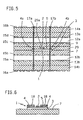
- the Fig. 1 and 2 illustrate an insert 1, hereinafter also referred to as an insert, for integration of an active electrical component 2, for example in the form of a chip, in a printed circuit board multilayer structure.
- the insert 1 contains a rewiring carrier layer 3 with rewiring applied thereon, consisting of rewiring contact points 4 and rewiring conductor tracks 5 for the electrical connection of the rewiring contact points 4, each with one connection lead 6, ie connection point, of the chip 2.
- the rewiring carrier layer 3 consists for example of a flexible printed circuit board material, such as an LCP Material or a polyimide film material with a thickness of eg 25 ⁇ m to 50 ⁇ m or a FR4 material with a thickness of eg 100 ⁇ m.
- a common ceramic material is usable.
- those materials are advantageous which are adapted in their coefficient of thermal expansion to the material of an adjacent layer and / or can absorb mechanical stresses in order to minimize mechanical stress loads for the insert 1.
- the chip 2 is mounted on an associated component mounting location in the center region of the rewiring carrier layer 3 and thus of the insert 1.
- an off-center chip mounting on the rewiring carrier layer 3 is possible, but the central positioning shown symmetrically and thus with respect to the lateral insert surface extension generally has advantages in terms of minimizing force loads due to mechanical stresses or thermal expansion effects in operational use.
- the chip assembly can be done by any conventional technique, such as a flip-chip mounting technique, as in Fig. 2 indicated, which then preferably includes a Unterschmaterial 8 in the space between the chip 2 and Umverottislic harsh.
- the fixation of the chip 2 takes place by means of connection techniques known per se, for example by thermode bonding, as represented by associated bonding sites on the chip terminals 6.
- the rewiring contact points 4 are arranged in a peripheral region on the redistribution carrier layer 3. Since there is more space available in this peripheral area, which is significantly larger in area than the central component mounting station, the rewiring 4, 5 simultaneously fulfills a terminal coarsening function, ie the rewiring contact points corresponding in their number to the chip terminal leads 6 4 can be arranged with a larger contact point extent and / or greater distance from one another than the chip connection leads 6, which facilitates the further contacting of the chip 2 via the rewiring contact points 4 to other electrically conductive structures and / or components of the printed circuit board multilayer structure and / or from the latter.
- the rewiring contact points 4 can be manufactured in a manner known per se together with the rewiring conductor tracks 5.
- component mounting location merely means that the relevant electrical component is to be placed there. This can be done by prefabricating the component separately and then bringing it to the component mounting station and fixing it there.
- the component can also be mounted directly on the component mounting station, e.g. be manufactured as an integrated semiconductor device structure and / or by screen printing or photolithographic processes.
- the rewiring conductor tracks 5 consist of narrow conductor tracks which are formed on the rewiring carrier layer 3 by one of the processes common for this purpose.
- the conductor tracks, which connect the chip connection points 6 to the rewiring contact points 4 are formed by wide, areal regions of an electrically conductive layer, which are applied over the entire area to the rewiring carrier layer 3 and then divided into areas separated from each other by a respective separation trench by a separation trench process becomes.
- the course of the separation trenches is chosen so that each of these surface areas one of the chip connection points 6 and the associated rewiring contact point 4 comprises and thereby represents their associated, connecting, planar conductor track.
- This embodiment variant has the advantage that the entire chip-side upper side of the rewiring carrier layer 3 remains covered except for the region of the chip 2 and the separation trenches with the redistribution layer, which consists, for example, of Cu, whereby on the one hand thermal expansion effects of the rewiring carrier layer 3 can be weakened and If desired, an adhesion promoter can be applied to the redistribution layer in order to improve the adhesion of a subsequent layer layer of the printed circuit board multilayer structure and to prevent any danger of delamination in the area of the insert 1.
- the structuring of the narrow conductor tracks 5 or, alternatively, the two-dimensional conductor tracks takes place, for example, by means of conventional photolithographic or laser structuring methods.
- thermally conductive material such as Cu
- electrically conductive redistribution layer it is advantageous to choose a good thermally conductive material, such as Cu, for the electrically conductive redistribution layer, since it can then additionally fulfill a heat-dissipating or heat-distributing function in order to prevent overheating in the area of the applied chip 2 during operation.
- an electromagnetic shielding of the rewiring layer or of the rewiring 4, 5 formed therefrom is realized by providing a shielding layer, for example by means of this and / or between the latter and the rewiring carrier layer 3 with the interposition of an electrically insulating layer. in the form of a whole-area, preferably metallic ground potential layer.
- the pre-fabricated insert piece 1 as explained above is then first with the underside for integration into a printed circuit board multilayer structure its rewiring support layer 3 on a backing layer 7 at a desired location in the lateral xy direction coordinates fixed.
- the fixation may be effected, for example, by means of one or more adhesive dots or a flat adhesive bond or by means of thermal loading of the rewiring carrier layer 3 itself and / or the region of the underlay layer 7 to be brought into contact therewith.
- the underlayer 7 represents a whole-area, electrically insulating dielectric layer of the multi-layer printed circuit board structure to be manufactured, which is made of a prepreg resin material or a liquid resin material. Said thermal application then leads to a partial melting, bonding and hardening of the prepreg underlay layer 7 in the region of the placed insert piece 1, whereby it is fixed.
- the backing layer 7 may be an outer or inner layer of the layer stack to be formed of several layers of the respectively desired printed circuit board multilayer structure.
- the further production of the printed circuit board multilayer structure involves the application of a full-surface covering layer on the provided with the insert piece 1 side of the backing layer 7 under cover of the insert piece 1, so that the latter lies between the backing layer 7 and the outer layer layer inside the layer stack of printed circuit board multilayer structure ,
- a full-surface covering layer on the provided with the insert piece 1 side of the backing layer 7 under cover of the insert piece 1, so that the latter lies between the backing layer 7 and the outer layer layer inside the layer stack of printed circuit board multilayer structure .
- On the top layer layer if selbige no outer layer layer of the printed circuit board multilayer structure represents, one or more further layer layers applied, and after stacking all provided for the layer stack layer layers of the layer stack is compressed or laminated together as a layer package in a conventional manner to form the desired printed circuit board multilayer structure.
- FIGS Fig. 1 to 9 Some specific examples of the integration according to the invention of such and similar insert pieces fitted with one or more active and / or passive electrical components into the interior of a printed circuit board multilayer structure are explained in more detail below.
- FIGS Fig. 1 to 9 For the sake of clarity and for better understanding, not only identical elements but also elements of the various exemplary embodiments which are equivalent in their function are shown in FIGS Fig. 1 to 9 each marked with the same reference numerals.
- Fig. 3 shows a substantially two-layer circuit board construction with two outer layers 7, 9 without inner layer, starting from the structure of the Fig. 1 and 2 the dielectric underlay layer 7 forms a first outer layer and a covering layer 9 applied thereto and the interposed insert 1 forms a second outer layer.
- the underlayer 7 and the cover layer 9 are each provided on the outside with an electrical conductor structure plane 10, 11, ie a structured electrical conductor plane, of conventional type, and are preferably made of a prepreg resin material.
- the insert piece 1 with its rewiring carrier layer 3, the chip 2 mounted thereon and the associated rewiring 4, 5 is embedded gap-free and void-free between the underlayer 7 and the cover layer 9 in its resin material.
- the chip 2 is contacted via the rewiring 4, 5 and blind hole contacts 12 to structural elements of the conductor level 11 on the cover layer 9, the through contacts 12 each one of the rewiring contact points 4 with the associated structural element of the conductor plane 11 through the dielectric cover layer 9 therethrough.
- the insert piece 1 prefabricated and fixed at the desired location on the prepreg support 7.
- the prepreg cover layer 9 is placed on the prepreg support 7 with the insert 1 fixed thereon.
- prepreg layers can be used for the two layers 7, 9, for example, which are provided with applied copper foils, which are subsequently patterned to form the conductor structure planes 10, 11.
- the layer package formed is compressed or laminated together in a customary manner to the composite layer stack overall for the purpose of completing the desired printed circuit board multilayer structure.
- the insert piece 1 is embedded in a gap-free and cavity-free manner in resin material which melts by the pressure of the press, or is received between the latter under corresponding impressions of the prepreg backing 7 and the prepreg cover layer 9. Since in this embodiment, the height of the insert piece 1 including the mounted thereon component 2 is relatively small, in particular much smaller than the layer thickness of the adjacent liquid resin prepreg or layers 7, 9, results from the embedding of the insert no significant bulge of the covering liquid resin or Prepreg füren 7, 9.
- a recess in the region of the insert piece 1 or at least mounted on it component 2 may be provided in accordance with space for receiving the insert piece 1 and the component 2 create.
- the structuring of the outer conductor planes 10, 11 is carried out after this pressing / lamination process, for example by a conventional lithography or laser structuring process.
- Fig. 3a shows a variant of the embodiment of Fig. 3 , in which a back- or underside backfilling of the chip 2 mounted in flip-chip technology is provided, which sits above the chip connection points 6 raised above the rewiring carrier layer 3.
- an underfill material 8a which is introduced from below via an underfill opening 8b introduced correspondingly into the insert piece 1.
- Fig. 3b shows a variant of the embodiment of Fig. 3 in which the insert piece 1 embedded in the resin material between the base layer 7 and the cover layer 9 is fitted on both sides with components.
- components mounted on the underside are shown, in particular, for example, a further chip 2a, an electrical resistor 2b and a capacitor element 2c or other active or passive electrical components.
- the lower-mounted electrical components 2a, 2b, 2c are coupled to a rear-side rewiring with contact points 4 'and redistribution conductors 5a, and the rear-side rewiring 4', 5a is connected via through-contacts 12a, which extend through the insert piece 1, with the upper-side rewiring 4, 5 electrically connected.
- this variant again corresponds to the exemplary embodiment of FIG Fig. 3 . so that reference may be made to the above remarks.
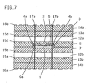
- Fig. 4 shows a further variant of the integration of the insert 1 in the interior of a printed circuit board multilayer structure, compared to the circuit board assembly of Fig. 3 additional inner layers 12a, 12b has.
- these are followed by an inner layer in the form of a prefabricated semi-finished printed circuit board 12a, 12b and two further prepreg layer layers 13a, 13b or 14a, 14b for completing the associated layer stack.
- an inner conductor pattern plane 15a to 15d is formed and embedded in the resin material of the adjacent prepreg layer layer.
- the two outer prepreg layer layers 14a, 14b each have an outer conductor pattern plane 16a, 16b on the outside.
- the lower layer layers are overlaid up to and including the backing layer 7 and the insert piece 1 fixed on the backing layer 7.
- the cover layer 9 is placed.
- the further layer layers are placed to form a corresponding layer package, which is then laminated or pressed together, whereby the insert piece 1 is securely embedded in the resin composition between the prepreg backing 7 and the prepreg cover layer 9.
- the contacting of the different conductor structure planes 15a to 16b and of the chip 2 on the insert piece 1 takes place in a customary manner by introducing corresponding through contacts.
- two through contacts 17a, 17b extending through associated structure elements of the two outer conductor structure planes 16a, 16b through the entire layer stack, which simultaneously contact associated rewiring contact points 4a, 4b and accordingly produce an electrical connection of associated terminals of the chip 2 to the outside, eg for power supply - or ground connection.
- the vias 17a, 17b are generated in a conventional technique by introducing corresponding through holes and introducing electrically conductive material into the same, for example by plating, wherein in the same operation, if necessary, an increase in thickness of the outer conductor structures 16a, 16b can be done.
- the contacting of the chip 2 to the outside via the rewiring contact points can also take place by introducing blind hole contacts reaching up to the rewiring contact points.
- FIG. 4 shows Fig. 4 an embodiment in which the base layer 7 and the cover layer 9 and consequently also the insert 1 embedded between them with the chip 2 mounted thereon are located in the middle of the circuit board layer stack, viewed in the stacking direction.
- Fig. 5 illustrates a variant of the embodiment of Fig. 4 in which the only significant difference is provided by an additional liquid resin or prepreg intermediate layer 29 in the stacked layer structure between the base layer 7 and the cover layer 9.
- this intermediate layer 29 is provided with a window region 29a, into which the component 2 protrudes.
- Laminating the structure also liquefies the resin material of the liquid resin or prepreg intermediate layer 29 and contributes to the complete gap-free enclosure of the insert piece 1 together with the assembled component 2 at.
- the intermediate layer 29 with the window 29a provides for receiving space of the chip 2 mounted on the insert piece 1 and thus facilitates homogeneous gap-free embedding of the insert piece between the two liquid resin or prepreg layers 7, 9 covering the bottom or top, without the latter being present Clearly bulge in the area of the insert piece 1.
- the intermediate layer 29 provides a relief of the chip 2 from the mechanical pressure loads acting during the pressing or laminating, which is advantageous, in particular, for relatively thin, pressure-sensitive chips.
- the intermediate layer 29 may also constitute a layer layer of a multilayer cover layer consisting of the cover layer 9 and the interlayer layer 29, in which case at least the intermediate layer 29, which lies on the side of this multilayer cover layer facing the insert piece 1, lies in this multilayer cover layer. is provided with the window 29a.
- the window 29a may extend over the entire area of the insert piece 1 if the latter requires a total of additional receiving space.
- Fig. 6 shows a variant with regard to the design of the insert piece 1.
- a structured height spacer layer 18 over the rewiring support layer 3 and the rewiring 4, 5 in the area outside the mounted chip 2 and with a little lateral distance from this on.
- the application of the height spacer layer 18 can be done before or after placing the insert 1 on the backing layer 7 as needed.
- the height spacer layer 18 extends from the rewiring carrier layer 3 or the rewiring 4, 5 from to at least the top of the assembled chip 2, in the example of Fig. 5 something as shown above.
- the height spacer layer 18 is capable of relieving the chip 2 from excessive compressive stresses in compressing the prepared layer stack in which the insert 1 is integrated.
- an epoxy resin material can be used as the material for the structured height-spacer layer 18 that can be produced, for example, by screen printing technology.
- a cutout in the region of the contact points 4 can be provided, which can be produced in a conventional manner, in order to avoid subsequent via problems or to improve the durability of the pressure contact, eg a copper sleeve.
- Fig. 7 illustrates the integration of an insert of the in Fig. 6 shown in a circuit board multilayer structure, which incidentally that of Fig. 4 corresponds, so that reference can be made to the above description.
- the cover layer 9 is provided with a matching recess 9a.
- a corresponding recess may be provided in the base layer 7.
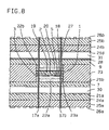
- Fig. 8 illustrates the integration of the insert 1 according to Fig. 6 in another example.
- the example of Fig. 8 includes the insert piece 1 starting from the structure according to Fig. 6
- a filling / planarization layer 19 which extends over the entire surface and with a substantially planar top over the height spacer layer 18 and the chip 2 and thereby also fills the lateral clearance between the chip 2 and the structured height spacer layer 18.
- an insert cover layer 20 is applied over the entire surface, which is identical in material and thickness to the rewiring support layer 3 or alternatively, this corresponds at least largely in thickness and in the thermal expansion behavior.
- the insert cap layer 20 may be e.g. how the rewiring support layer 3 is made of a polyimide material or a ceramic material.
- the insert piece 1 rests on a buffer layer piece 22a which is formed of a material which can compensate for mechanical stresses, in particular due to thermal stresses, or mediate between the thermal expansion coefficients of the upper-side rewiring carrier layer 3 of the insert 1 and an electrically conductive layer adjoining on the underside ,
- the buffer layer piece may consist of an epoxy resin material.
- the buffer layer piece 22a in this example rests on the base layer 7, which in turn lies on an inner layer 30 provided with conductor track structures on both sides.
- the buffer layer piece 22a can be produced, for example, by screen printing or cut out of a corresponding layer material and placed on the relevant layer on the backing layer 7 and fixed.
- the insert piece 1 with the described structure.
- Next includes the layer structure of Fig. 8 above the backing layer 7 a liquid resin or Prepreg intermediate layer 23 with a window portion 23a, in which the insert piece 1 including buffer layer piece 22a is received.
- the window 23a is cut or milled out in the size of the buffer layer piece 22a whose lateral dimension corresponds to that of the insert piece, and the lateral gap to the insert piece 1 then fills with molten resin material during later pressing.
- the buffer layer piece 22a it may be advantageous to provide a corresponding buffer layer piece 22b as part of the insert 1 between the latter and the cover layer 9 in order to compensate for thermal or mechanical loads, as also shown in FIG Fig. 8 shown.
- a corresponding buffer layer piece 22b as part of the insert 1 between the latter and the cover layer 9 in order to compensate for thermal or mechanical loads, as also shown in FIG Fig. 8 shown.
- the symmetrical arrangement of the upper buffer layer piece 22b to the lower buffer layer piece 22a preferably using substantially equal layer thicknesses and the same or thermal expansion similar materials, another contribution to minimizing the force loads on the insert 1 with its chip 2.
- Another is the printed circuit board multilayer construction of Fig. 6 Overall, in turn, with respect to a stack center plane largely symmetrical nature, and the insert 1 with the chip 2 is seen in the stacking direction in the middle region of the multi-layer structure.
- each of the unitarily illustrated liquid resin or prepreg layers which function as a backing layer and cover layer for covering the insert on both sides, ie in this example layers 7 and 9, and / or the intervening intermediate layer, ie in this example the intermediate layer 23, can each be constructed in multiple layers with at least 2 liquid resin or prepreg layer layers.
- the example according to Fig. 8 has in addition to the lower inner layer or semi-finished circuit board 30 and an upper inner layer or upper semi-finished circuit board 31 with overhead Porter Modellebende 21 d.
- Each of the prepregs 24a, 24b and an outer dielectric layer layer 25a, 25b follows downwards or upwards.
- the outer dielectric layer layers 25a, 25b bear on the outside each an outer conductor pattern plane 26a, 26b, for which they can consist of a prepreg material and a resting copper foil.
- the copper foil is firmly bonded to the prepreg material and the resulting copper layer is patterned in the course of common process steps in the corresponding conductor structure plane 26a, 26b.
- the insert piece 1 has a highly thermally conductive layer 27, for example made of Cu, between the filling / planarizing layer 19 and the insert covering layer 20.
- a highly thermally conductive layer 27 for example made of Cu
- an inner conductor structure plane of the upper semifinished product circuit board 31 is replaced by an unstructured, all-surface heat-conducting layer 28, which may simply be an unstructured copper coating of this semifinished product circuit board 9a, for example.
- vias 17a, 17b additionally a heat transport function by being made of a good thermal conductivity material, such as Cu. Because of the vias 17a, 17b are the associated rewiring contact points and especially the heat conduction layer 27 of the insert 1 with the whole-surface heat-conducting layer 28 of the layer stack in heat-conducting connection, so that very effectively heat, which is formed in the region of the chip 2, via the rewiring 4th 5, on the one hand, and the filling / planarizing layer 19 and the insert heat conducting layer 27, on the other hand, are conducted to the through contacts 17a, 17b and can be dissipated via this to the heat-conducting layer 28 over the entire surface and distributed therefrom.
- a good thermal conductivity material such as Cu.
- This heat dissipation measure can significantly increase the reliability of the function of the chip 2 mounted on the embedded insert 1 and the remaining insert components, especially in cases where appreciable heat generation of components of the insert 1 during operation is caused. It is self-evident that, for the heat-conducting connection to the heat-conducting layer 28 of the layer stack, in each case potential-identical through-contacts are suitable, such as common ground or voltage supply through contacts.
- the insert heat-conducting layer 27 may, for example, already pre-fabricated on the insert top layer 20 of polyimide or the like Layer be made of copper, for example.
- the insert cover layer 20 can be cut out together with the heat-conductive coating 27 of a larger-area layer material and placed with the coating 27 on the filling / planarization layer 19. This can be done as needed before positioning the insert 1 on the backing layer 7 or thereafter.
- the through contacts 17a, 17b without contact with the material of the rewiring carrier layer 3, e.g. Polyimide, pass through it.
- the material of the rewiring carrier layer 3 e.g. Polyimide
- bores are then introduced into the rewiring carrier layer 3 before the embedding of the insert piece 1 between the underlay layer 7 and the cover layer 9 with a larger diameter compared to the later through contacts.
- these holes fill with flowing in resin material from the adjacent resin layer layer.
- the through holes of smaller diameter introduced therethrough after pressing the layer stack can then extend completely within the resin filling at the level of the rewiring carrier layer 3, so that an insulating resin material ring remains between the introduced through contact material and the material of the rewiring carrier layer 3.
- Fig. 9 shows as a further embodiment of the invention a variant of the example of Fig. 5 in which a window area 32a is additionally provided in an inner layer 32 as the sole significant difference for receiving the insert piece 1, on which in this example a comparatively thick, eg, housed, chip 2 or another cased or, for other reasons, relatively thick electrical component is mounted is.
- this inner layer 32 is located in the interior of a multilayer intermediate layer between the backing layer 7, on which the insert piece 1 rests, and the cover layer layer 9.
- the intermediate layer here contains the liquid resin or prepreg intermediate layer 29 as a lower layer layer, the inner layer 32 as a middle layer layer and an upper liquid resin or prepreg layer layer 29b.
- the window 29a of the lower intermediate layer 29 and the window 32a of the inner layer 32 together form a receiving space.
- the upper interlayer ply 29b provides for the upper resin coverage of the insert 1 with the chip 2.
- the insert piece with the chip 2 is embedded on all sides without gaps in surrounding resin material, which in this case comes from the underlay layer 7, the lower interlayer ply 29 and the upper interlayer ply 29b and any gaps especially between the relatively thick chip 2 and the laterally adjacent window edge regions the lower intermediate layer layer 29 and the inner layer 32 fills by liquefying during compression or lamination of the structure and filled corresponding spaces.
- the windows can be provided with lateral dimensions which are at least approximately those of the rest of the insert piece 1, ie in particular of the below the chip 2 layer structure with the redistribution carrier layer 3 in order to also accommodate this part of the insert 1 in a window area, if required.
- This is expedient in particular in the case of a higher insert piece layer structure, as for example in the case of insert pieces of the type described in US Pat Fig. 8 shown, especially if this is still relatively thick mounted components such as the chip 2 of Fig. 9 includes.
- the invention also comprises printed circuit board multi-layer structures, in which an insert with several provided on him, active and / or passive electrical components and / or multiple inserts with one or more electrical components in the interior of the layer stack are integrated.
- a plurality of inserts may be positioned side by side in the same stacking plane with lateral spacing.
- a plurality of insert pieces may be positioned one above the other in the stacking direction in different stacking planes with or without lateral offset.
- the invention enables a very advantageous integration of one or more insert pieces, each having one or more passive and / or active electrical components on a rewiring support layer into the interior of a printed circuit board multilayer structure, wherein the insert piece and in particular its rewiring support layer completely and is embedded gap-free in resin material between a pad and a cover layer, for example, prepreg resin material.
- the structure of the insert and its incorporation into the stack of layers can be realized on request with a high degree of symmetry, which prevents high mechanical stress due to thermal expansion effects at significant temperature changes.
- the rewiring carrier layer of the insert Since the rewiring carrier layer of the insert has a significantly smaller surface area than the embedding layer layers of the printed circuit board layer stack, no delamination problems occur, as might be feared when introducing a continuous rewiring carrier layer, for example made of polyimide.
- a flexible, thin design of the rewiring carrier layer can further contribute to tensile and compressive force stresses occurring due to an interposer effect due to different thermal expansion coefficients of the Compensate involved layer materials.
- a substantially central or symmetrical placement of the component or components on the rewiring carrier layer of the insert also contributes to the reduction of lateral tensile and compressive force loads.
- the printed circuit board multilayer structure according to the invention is relatively easy to produce according to the invention.
- the redistribution substrate layer and the electrical component (s) mounted thereon may be electrically tested prior to crimping the layer stack, which reduces the error rate and improves yield.
- Only electrically functional components are fitted to the redistribution carrier layer, and only functionally assembled insert pieces are laid in the layer stack of the printed circuit board multilayer structure and pressed with this. Due to the segmented introduction of the redistribution only in the portion of the layer stack in which the insert between the dielectric underlayer and the dielectric cover layer is located, can also increase the overall packing density of the printed circuit board multilayer structure.
- the inventive rewiring in the interior of the printed circuit board multilayer structure also space requirements can be reduced to outer layers, and the unbundling of the outer layers simplified, since only corresponding vias are to be led by the rewiring contact points to the surface and the position of the rewiring contact points can be selected in that the associated through-contacts to the outer layers are located at a position which is optimal for the unbundling of the outer layers.
Landscapes
- Engineering & Computer Science (AREA)
- Microelectronics & Electronic Packaging (AREA)
- Computer Hardware Design (AREA)
- Power Engineering (AREA)
- Production Of Multi-Layered Print Wiring Board (AREA)
- Manufacturing Of Printed Wiring (AREA)
Description
Die Erfindung bezieht sich auf einen Leiterplatten-Mehrschichtaufbau nach dem Oberbegriff des Anspruchs 1 sowie auf ein zugehöriges Herstellungsverfahren. Der Begriff elektrisches Bauteil umfasst hierbei auch elektronische Bauteile.The invention relates to a printed circuit board multilayer structure according to the preamble of
Leiterplatten-Mehrschichtaufbauten mit einem Schichtstapel aus mehreren elektrisch isolierenden und/oder mit Leiterbahnstrukturen versehenen Schichten und wenigstens einem passiven oder aktiven elektrischen Bauteil im Inneren des Schichtstapels gewinnen in jüngerer Zeit immer mehr an Bedeutung, um passive elektrische Bauteile, wie Kondensatoren und Widerstände, und/oder aktive elektrische Bauteile, wie Halbleiterchips, im Inneren einer Leiterplatte vom sogenannten Mehrschicht- oder Multilayertyp zu integrieren. Der Mehrschichtaufbau umfasst einen Schichtstapel aus mehreren übereinanderliegenden, elektrisch isolierenden bzw. dielektrischen Schichten, z.B. aus einem Prepreg-Harzmaterial, mit zwischenliegenden elektrischen Leiterstrukturebenen, die geeignete Trägerschichten mit aufgebrachten Leiterbahnstrukturen beinhalten. Der Schichtstapel wird z.B. durch Laminieren bzw. Verpressen unter Verwendung dielektrischer Prepreg-Schichten fertiggestellt, wobei wenigstens ein Teil der übereinandergelegten Schichten ein- oder beidseitig mit einer elektrisch leitenden Schicht versehen ist, die vor dem Übereinanderlegen zum Schichtstapel in ein gewünschtes elektrisches Leiterbild strukturiert wird. Häufig wird für diesen Zweck für sogenannte Innenlagen, d.h. im Inneren des Schichtstapels befindliche, mit Leiterbahnstrukturen versehene Schichten, ein Epoxidharz als Trägerschichtmaterial mit einer Kupferkaschierung benutzt. Zur Strukturierung der sogenannten Außenlagen, d.h. der außenliegenden, mit Leiterbahnstrukturen versehenen Schichten, wird meist auf eine dielektrische Prepregschicht eine Kupferfolie aufgelegt, die durch den Verpressvorgang fest mit der Prepregschicht verbunden wird.Circuit board multilayer structures with a layer stack comprising a plurality of electrically insulating and / or conductor tracked layers and at least one passive or active electrical component in the interior of the layer stack have recently become increasingly important in order to detect passive electrical components such as capacitors and resistors. or to integrate active electrical components, such as semiconductor chips, inside a printed circuit board of the so-called multi-layer or multilayer type. The multilayer structure comprises a layer stack of a plurality of superimposed, electrically insulating or dielectric layers, for example of a prepreg resin material, with interposed electrical conductor structure planes which contain suitable carrier layers with applied conductor track structures. The layer stack is completed, for example, by laminating or pressing using prepreg dielectric layers, wherein at least a part of the superimposed layers is provided on one or both sides with an electrically conductive layer, which is patterned into a desired electrical pattern before stacking to form the layer stack. Frequently, an epoxy resin is used as a carrier layer material with a Kupferkaschierung for this purpose for so-called inner layers, that is provided in the interior of the layer stack, provided with interconnect layers, an epoxy resin. For structuring the so-called outer layers, ie the outer, With layers provided with conductor track structures, a copper foil is usually applied to a dielectric prepreg layer, which is firmly connected to the prepreg layer by the pressing process.
Für eine solche Integration eines aktiven und/oder passiven elektrischen Bauteils in eine Leiterplatte ist es bekannt, selbiges auf einer mit Leiterbahnen versehenen, elektrisch isolierenden Unterlagenschicht in einem leiterbahnfreien Bereich zu fixieren, bevor dann eine oder mehrere weitere Schichten zur Fertigstellung des Schichtstapels aufgebracht werden und der Gesamtaufbau zusammenlaminiert bzw. verpresst wird. Dabei schließt sich an die das Bauteil tragende Unterlagenschicht üblicherweise eine nächste dielektrische Schicht an, die ganzflächig ausgeführt oder im Bereich des elektrischen Bauteils mit einem Fenster- oder Ausnehmungsbereich versehen ist. Dabei wird vorliegend unter einem Fenster eine die betreffende Schicht vollständig durchdringende Öffnung verstanden, unter einer Ausnehmung hingegen eine einseitig nur in eine Tiefe kleiner als die Schichtdicke in der betreffenden Schicht gebildete Aussparung. Die Kontaktierung von Anschlusskontaktstellen des elektrischen Bauteils zu Leiterstrukturen auf der Unterlagenschicht oder zu Leiterstrukturen in anderen Ebenen des Schichtstapels erfolgt mit Hilfe von Durchkontakten, worunter vorliegend der Einfachheit halber auch Sacklochkontakte verstanden werden sollen, die auf den Kontaktstellen enden. Alternativ wird das elektrische Bauteil in einem elektrischen Kontaktierungsbereich der Unterlagenschicht auf dieser fixiert und direkt mit dortigen Leiterstrukturen elektrisch verbunden. Leiterplatten-Mehrschichtaufbauten dieser verschiedenen Typen sind beispielsweise in der Offenlegungsschrift
In der Offenlegungsschrift
In der Patentschrift
In der Patentschrift
Der Erfindung liegt als technisches Problem die Bereitstellung eines Leiterplatten-Mehrschichtaufbaus der eingangs genannten Art und eines zugehörigen Herstellungsverfahrens zugrunde, die es ermöglichen, ein oder mehrere elektrische Bauteile im Inneren des Mehrschichtaufbaus mit relativ geringem Aufwand und hoher Funktionszuverlässigkeit zu integrieren.The invention is based on the technical problem of providing a printed circuit board multilayer structure of the aforementioned type and an associated manufacturing method, which make it possible to integrate one or more electrical components in the interior of the multi-layer structure with relatively little effort and high reliability.
Die Erfindung löst dieses Problem durch die Bereitstellung eines Leiterplatten-Mehrschichtaufbaus mit den Merkmalen des Anspruchs 1 und eines Herstellungsverfahrens mit den Merkmalen des Anspruchs 19.The invention solves this problem by providing a printed circuit board multilayer structure having the features of
Beim erfindungsgemäßen Leiterplatten-Mehrschichtaufbau ist das Insertstück mit seiner gegenüber dem Schichtstapel geringeren Flächenausdehnung allseitig, auch lateral, vollständig eingebettet, und zwar von zwei abdeckenden Prepeg- oder Flüssigharz-Schichten, einer Prepreg- oder Flüssigharzunterlagenschicht einerseits und einer Prepreg- oder Flüssigharzdecklagenschicht andererseits, und von Harzmaterial, das sich beim Verpressen oder Laminieren des Aufbaus in an das Insertstück angrenzenden Prepeg- oder Flüssigharz-Schichtbereichen verflüssigt und dadurch Spalte oder Zwischenräume zwischen dem Insertstück und benachbarten Bereichen des Schichtstapels verfüllt bzw. ausfüllt. Dadurch lässt sich das Insertstück komplett und spaltfrei in eine homogene Harzumgebung einbetten.In the case of the printed circuit board multilayer structure according to the invention, the insert piece is completely embedded on all sides, including laterally, by two covering prepreg or liquid resin layers, a prepreg or liquid resin underlay layer on the one hand and a prepreg or liquid resin covercoat layer on the other hand, and of resin material that liquefies upon compression or lamination of the assembly into prepreg or liquid resin layer regions adjacent the insert, thereby filling or filling gaps or spaces between the insert and adjacent regions of the layer stack. This allows the insert to be completely and gap-free embedded in a homogeneous resin environment.
Es versteht sich, dass die im Schichtstapel verwendeten Flüssigharz- oder Prepreg-Schichten nach dem Verpressen oder Laminieren des Aufbaus entsprechend ausgehärtete, elektrisch isolierende bzw. dielektrische Schichten bilden, wie dem Fachmann geläufig. Der Übersichtlichkeit halber werden diese Schichten vorliegend auch in ihrem endfertigen, ausgehärteten Zustand weiterhin als Flüssigharz- bzw. Prepreg-Schichten bezeichnet.It is self-evident that the liquid resin or prepreg layers used in the layer stack form correspondingly hardened, electrically insulating or dielectric layers after pressing or laminating the structure, as is familiar to the person skilled in the art. For the sake of clarity, these layers are also referred to as liquid resin or prepreg layers in their final, cured state.
In einer Weiterbildung der Erfindung nach Anspruch 2 weist wenigstens eine der beiden das Insertstück abdeckenden Flüssigharz- bzw. Prepreg-Schichten eine Ausnehmung auf, in der das Insertstück oder das oder die auf ihm montierten Bauteile Platz finden, d.h. mit wenigstens einem Teil ihrer Höhenerstreckung aufgenommen werden können. Dies kann das Aufnehmen von Insertstücken bzw. Bauteilen mit etwas größerer Höhe erleichtern, ist aber gerade auch für empfindliche Insertstücke bzw. Bauteile geringer Dicke von Vorteil, um für diese eine mechanische Druckentlastung beim Press-/Laminiervorgang bereitzustellen.In a further development of the invention according to
In einer weiteren vorteilhaften Weiterbildung der Erfindung ist gemäß Anspruch 3 zwischen den beiden das Insertstück abdeckenden Flüssigharz- oder Prepreg-Schichten eine Flüssigharz- oder Prepreg-Zwischenschicht vorgesehen, die ein Fenster im Bereich des Insertstücks oder wenigstens eines auf ihm montierten Bauteils aufweist. Auch diese Realisierungsvariante der Erfindung kann insbesondere für Insertstücke bzw. darauf montierte elektrische Bauteile mit relativ großer Höhe, z.B. wenn letztere in der Größenordnung der typischen Schichtdicken der einzelnen Schichten des Schichtstapels liegt, aber auch für dünne, druckempfindliche Insertstücke bzw. darauf montierte elektrische Bauteile von Vorteil sein. Die Zwischenschicht vermeidet stärkere Auswölbungen der abdeckenden Flüssigharz- oder Prepreg-Schichten im Fall eines relativ hohen Insertstücks bzw. darauf montierten elektrischen Bauteils und sorgt bei dünnen druckempfindlichen Inserts bzw. darauf montierten Bauteilen für eine Druckentlastung beim Verpressen des Aufbaus. Die komplette und spaltfreie Einbettung des Insertstücks in beim Verpressen oder Laminieren des Aufbaus verflüssigtes, angrenzendes Harzmaterial bleibt gewährleistet, wobei letzteres in diesem Fall wenigstens teilweise auch aus der Zwischenschicht stammen kann.In a further advantageous development of the invention, a liquid resin or prepreg intermediate layer is provided between the two liquid resin or prepreg layers covering the insert piece, which has a window in the region of the insert piece or at least one component mounted on it. This implementation variant of the invention can also be used, in particular, for insert pieces or electrical components of relatively high height mounted thereon, e.g. if the latter is of the order of magnitude of the typical layer thicknesses of the individual layers of the layer stack, but also for thin, pressure-sensitive inserts or electrical components mounted thereon. The interlayer avoids more bulging of the covering liquid resin or prepreg layers in the case of a relatively high size insert or electrical component mounted thereon, and provides pressure relief upon compression of the assembly with thin pressure sensitive inserts or components mounted thereon. The complete and gap-free embedding of the insert in liquefied during compression or lamination of the structure, adjacent resin material remains guaranteed, the latter in this case can at least partially originate from the intermediate layer.
In einer Weiterbildung der Erfindung nach Anspruch 4 sind die beiden das Insertstück abdeckenden Flüssigharz- oder Prepreg-Schichten und/oder die Flüssigharz- oder Prepreg-Zwischenschicht mehrlagig gebildet und beinhalten dabei wenigstens zwei Flüssigharz- oder Prepreg-Schichtlagen. Dabei kann je nach Fall die Zwischenschicht auch eine Flüssigharz- oder Prepreg-Schichtlage einer der beiden das Insertstück abdeckenden Flüssigharz- oder Prepreg-Schichten darstellen. Bei mehrlagigem Aufbau kann eine Ausnehmung in einer der beiden Flüssigharz- oder Prepreg-Schichten im Bereich des Insertstücks oder eines auf ihm montierten Bauteils z.B. dadurch realisiert sein, dass wenigstens eine der Schichtlagen auf der dem Insertstück zugewandten Seite der betreffenden Flüssigharz- oder Prepreg-Schicht mit einem Fenster versehen ist. Eine anschließende, durchgehende Schichtlage schließt dann den vom Fenster gebildeten Aufnahmeraum in Schichtstapelrichtung ab. Bei Bedarf kann optional in dieser abdeckenden Schichtlage zusätzlich noch eine Ausnehmung vorgesehen sein.In a further development of the invention according to
In einer Weiterbildung der Erfindung nach Anspruch 5 befindet sich zwischen den beiden das Insertstück abdeckenden Flüssigharz- oder Prepreg-Schichten wenigstens eine mit Leiterbahnstrukturen versehene Schicht, d.h. eine Innenlage, die ein Fenster im Bereich des Insertstücks oder des oder der auf ihm montierten Bauteile aufweist. Mit anderen Worten erstreckt sich in diesem Ausführungsbeispiel der Aufnahmeraum für das Insertstück bzw. das betreffende Bauteil durch eine Innenlage hindurch, wodurch auch Insertstücke bzw. darauf montierte Bauteile mit vergleichsweise großer Höhe in den Schichtstapel vorteilhaft integriert werden können. Das spaltfreie Einbetten in Harzmaterial aus angrenzenden Flüssigharz- oder Prepreg-Schichtbereichen ist auch in diesem Ausführungsbeispiel gegeben, wobei in diesem Fall das beim Verpressen oder Laminieren des Aufbaus verflüssigte Harzmaterial aus angrenzenden Flüssigharz- oder Prepreg-Schichtbereichen auch jeglichen lateralen Spalt zwischen dieser Innenlage und dem Insertstück bzw. dem darauf montierten Bauteil vollständig ausfüllt.In a development of the invention according to
In einer Weiterbildung nach Anspruch 6 ist das wenigstens eine elektrische Bauteil auf einem Bauteilmontageplatz einer Umverdrahtungsträgerschicht des Insertstücks montiert, auf der auch die Umverdrahtung vorgesehen ist, wobei sich letztere in einer weiteren Ausgestaltung gemäß Anspruch 7 auf der gleichen Seite dieser Schicht befindet wie der Bauteilmontageplatz. Das Insertstück befindet sich im Inneren des Schichtstapels und erstreckt sich lateral nur in einem Teilbereich der Flächenausdehnung des Schichtstapels. Mit anderen Worten ist das elektrische Bauteil in diesem Fall Bestandteil eines Insertstücks, das in das Innere des Schichtstapels integriert ist und eine Trägerschicht mit Umverdrahtungsfunktion für das elektrische Bauteil beinhaltet. In vorteilhafter Ausgestaltung kann gemäß Anspruch 8 eine beidseitige Bauteilbestückung mit jeweils zugehöriger Umverdrahtung für das Insertstück vorgesehen sein, wobei Durchkontakte für eine elektrische Kontaktierung der beiden Umverdrahtungen sorgen.In a development according to
Die Erfindung ermöglicht eine vorteilhafte Vormontage des elektrischen Bauteils auf der Umverdrahtungsträgerschicht und ein elektrisches Prüfen des Insertstücks, d.h. insbesondere des elektrischen Bauteils und seiner Umverdrahtung, vor Einbau in den Schichtstapel. Dies gewährleistet, dass das Insertstück nur mit funktionsfähigen elektrischen Bauteilen bestückt wird und nur fehlerfrei bestückte und ordnungsgemäß arbeitende Insertstücke in den Mehrschichtaufbau eingebracht werden. Die Umverdrahtung ermöglicht eine Vergröberung von Anschlussstrukturen für die Kontaktierung des oder der Bauteile mit Leiterstrukturen des Schichtstapels oder nach außen, d.h. entsprechende Kontaktflächen können größer und/oder mit größerem Abstand voneinander angeordnet werden als die jeweils direkt am Bauteil vorhandenen Anschlusskontakte. Dies mindert die Anforderungen hinsichtlich Positioniergenauigkeit für einzubringende Sackloch- oder Durchkontakte. Da die Umverdrahtung auf dem Insertstück realisiert ist, braucht sie nicht auf einer der Leiterebenen des Schichtstapels erzeugt werden und das jeweilige elektrische Bauteil braucht nicht auf einer solchen Leiterstrukturebene an entsprechender Stelle hochgenau positioniert werden, was den Fertigungsaufwand verringert und die Funktionszuverlässigkeit erhöht.The invention enables advantageous pre-assembly of the electrical component on the redistribution substrate layer and electrical testing of the insert, i. in particular of the electrical component and its rewiring, prior to installation in the layer stack. This ensures that the insert is fitted only with functional electrical components and only correctly assembled and properly working insert pieces are introduced into the multi-layer structure. The redistribution enables coarsening of connection structures for contacting the component or components with conductor structures of the layer stack or to the outside, i. corresponding contact surfaces can be larger and / or arranged at a greater distance from each other than the respective directly on the component existing connection contacts. This reduces the requirements with regard to positioning accuracy for blind hole or through contacts to be introduced. Since the rewiring is realized on the insert piece, it does not need to be generated on one of the conductor levels of the layer stack and the respective electrical component need not be positioned on such a ladder structure level in the appropriate place highly accurate, which reduces the manufacturing cost and increases the reliability of the function.
Die Realisierung der Umverdrahtung auf dem in das Innere des Leiterplatten-Mehrschichtaufbaus integrierten Insertstück und speziell auf der Chipmontageseite der Umverdrahtungsschicht hat den weiteren Vorteil, dass sich der Platzbedarf auf der oder den Außenlagen des Mehrschichtaufbaus verringern lässt, da nur noch die entsprechenden Durchkontakte an die Oberfläche des Mehrschichtaufbaus zu führen sind. Zudem vereinfacht sich eine Entflechtung der Außenlagen, da die Position der Umverdrahtungskontaktstellen auf der Umverdrahtungsträgerschicht so gewählt werden kann, dass die zugehörigen Durchkontakte zu den Außenlagen an eine für die Entflechtung der Außenlagen günstigen Stelle platziert werden können.The implementation of the rewiring on the integrated into the interior of the printed circuit board multilayer structure insert and especially on the Chip mounting side of the redistribution layer has the further advantage that the space required on the or the outer layers of the multi-layer structure can be reduced, since only the corresponding vias are to be led to the surface of the multi-layer structure. In addition, unbundling of the outer layers is simplified, since the position of the rewiring contact points on the rewiring carrier layer can be selected such that the associated vias to the outer layers can be placed at a location favorable for the unbundling of the outer layers.
Da das Insertstück bzw. deren Umverdrahtungsträgerschicht sich nur über einen lateralen Teilbereich des Schichtstapels erstreckt, werden Delaminationsprobleme verhindert, selbst wenn die Haftfähigkeit z.B. einer Umverdrahtungsträgerschicht aus Polyimid an einem Prepregmaterial der angrenzenden Unterlagenschicht nicht besonders hoch sein sollte.Since the insert or its rewiring support layer extends only over a lateral portion of the layer stack, delamination problems are prevented even if the adhesiveness is e.g. a rewiring carrier layer of polyimide should not be particularly high on a prepreg material of the adjacent underlayer.
Die Umverdrahtungsträgerschicht kann z.B. als flexible, dünne Schicht mit Interposer-Wirkung realisiert werden. Diese Maßnahme trägt dazu bei, mechanische Spannungen gering zu halten, die durch thermische Ausdehnungseffekte verursacht werden. Dies ist besonders dann von Bedeutung, wenn signifikante Temperaturänderungen des Schichtstapels im Betrieb oder bei der Weiterverarbeitung auftreten.The redistribution carrier layer may be e.g. be realized as a flexible, thin layer with interposer effect. This measure helps to minimize mechanical stresses caused by thermal expansion effects. This is particularly important if significant temperature changes of the layer stack occur during operation or during further processing.
In einer vorteilhaften Weiterbildung der Erfindung nach Anspruch 9 besteht die Umverdrahtungsträgerschicht aus einem flexiblen Leiterplattenmaterial, wie einem Flüssigkristallpolymer(LCP)- oder Polyimidmaterial, oder einem Keramikmaterial und sie weist in einem mittleren Bereich einen Bauteilmontageplatz für das oder die zu montierenden elektrischen Bauteile und in einem peripheren Bereich Umverdrahtungskontaktstellen auf, die mit dem Bauteilmontageplatz über zugehörige Leiterbahnen elektrisch verbunden sind. Die mittige Bauteilplatzierung auf der Umverteilungsträgerschicht trägt ebenfalls zur Kompensation von thermischen Ausdehnungskräften bei, da sich auf diese Weise laterale Zug- und Druckkräfte weitestgehend aufheben. Die Umverdrahtung vom mittigen Bauteilmontageplatz zum peripheren Trägerschichtbereich leistet zudem eine Vergröberung der Anschlussstruktur des Bauteils, da im peripheren Bereich mehr Platz für Kontaktstellen zur Verfügung steht.In an advantageous embodiment of the invention according to
In einer Weiterbildung der Erfindung nach Anspruch 10 ist zwischen dem Insertstück einerseits und wenigstens einer der als Unterlagenschicht bzw. Deckschicht fungierenden, das Insertstück beidseitig abdeckenden Flüssigharz- oder Prepeg-Schichten ein jeweiliges Pufferschichtstück vorgesehen, wobei sich dieses Pufferschichtstück nur über eine laterale Teilfläche des Schichtstapels erstreckt, vorzugsweise allenfalls wenig größer als das Insertstück, und hinsichtlich Material und Schichtdicke z.B. so gewählt sein kann, dass es zwischen dem thermischen Ausdehnungskoeffizienten der Umverdrahtungsträgerschicht des Insertstücks und demjenigen der Unterlagenschicht bzw. Deckschicht vermittelt und/oder mechanische Spannungen aufnehmen kann und/oder in der Lage ist, Leiterstrukturen an einer dem Insertstück gegenüberliegenden Oberfläche der Unterlagenschicht bzw. der Deckschicht elektrisch gegenüber dem Insertstück zu isolieren.In a further development of the invention, a respective buffer layer piece is provided between the insert piece on the one hand and at least one of the liquid resin or prepeg layers covering the insert piece on both sides, whereby this buffer layer piece only extends over a lateral partial surface of the layer stack extends, preferably at most slightly larger than the insert, and in terms of material and layer thickness, for example may be chosen such that it mediates between the coefficient of thermal expansion of the rewiring carrier layer of the insert and that of the underlayer and / or cover layer and / or can absorb mechanical stresses and / or is capable of conducting structures on a surface opposite the insert surface of the underlayer or the Insulate cover layer electrically opposite the insert piece.
In einer Weiterbildung der Erfindung nach Anspruch 11 ist auf der Umverdrahtungsträgerschicht in einem Bereich lateral außerhalb des oder der montierten elektrischen Bauteile eine Höhenabstandshalterstruktur vorgesehen, die sich in Stapelrichtung so weit wie das oder die montierten elektrischen Bauteile oder über diese hinaus erstreckt. Die Höhenabstandshalterstruktur kann dadurch das oder die montierten elektrischen Bauteile von beim Verpressen des Mehrschichtaufbaus einwirkenden Druckkräften entlasten.In a development of the invention according to
In einer Weiterbildung der Erfindung nach Anspruch 12 beinhaltet das Insertstück zusätzlich eine Füll- und/oder Planarisierungsschicht, die sich ganzflächig oder nur im Bereich außerhalb des oder der elektrischen Bauteile über der Umverdrahtungsträgerschicht erstreckt. Diese ist in der Lage, bei Bedarf größere Höhenunterschiede des Insertstücks aufgrund des oder der aufgebrachten Bauteile auszugleichen bzw. laterale Freiräume aufzufüllen. Insbesondere ist diese Schicht bei Vorhandensein der Höhenabstandshalterstruktur auch in der Lage, Freiräume zwischen dieser Struktur und dem oder den montierten elektrischen Bauteilen auszufüllen.In a further development of the invention according to
In einer Ausgestaltung dieser Maßnahme besteht die Füll- und/oder Planarisierungsschicht gemäß Anspruch 13 aus einem thermisch leitfähigen, jedoch elektrisch isolierenden Material. Dies ermöglicht bei Bedarf eine Wärmeabführung von dem oder den elektrischen Bauteilen.In one embodiment of this measure, the filling and / or planarization layer according to claim 13 consists of a thermally conductive, but electrically insulating material. This allows, if necessary, a heat dissipation of the one or more electrical components.
In einer weiteren Ausgestaltung der Maßnahme, eine Füll- und/oder Planarisierungsschicht aus thermisch leitfähigem Material vorzusehen, umfasst das Insertstück gemäß Anspruch 14 eine Wärmeleitschicht über der Füll- und/oder Planarisierungsschicht in Wärmekontakt zu derselben. Damit kann z.B. von dem oder den montierten elektrischen Bauteilen im Betrieb entwickelte Wärme effektiv über die Füll- und/oder die Planarisierungsschicht und die darüber liegende Wärmeleitschicht abgeführt bzw. verteilt werden.In a further embodiment of the measure, to provide a filling and / or planarization layer of thermally conductive material, the insert piece according to claim 14 comprises a heat conducting layer over the filling and / or planarization in thermal contact with the same. Thus, e.g. Heat developed by the mounted electrical component (s) during operation is effectively dissipated or distributed through the fill and / or planarization layer and the overlying thermal conductive layer.
In einer weiteren Ausgestaltung weist gemäß Anspruch 15 das Insertstück eine Deckschicht über der Füll- und/oder Planarisierungsschicht bzw. der Wärmeleitschicht auf, wobei die Deckschicht hinsichtlich Material und/oder Größe in lateraler Richtung und Stapelrichtung gleichartig zur Umverdrahtungsträgerschicht gewählt ist. Damit erhält das Insertstück einen vergleichsweise symmetrischen Schichtaufbau, was ebenfalls dazu beiträgt, mechanische Spannungen aufgrund von Ausdehnungseffekten gering zu halten und Biegebeanspruchungen zu minimieren.In a further embodiment, according to claim 15, the insert has a cover layer over the filling and / or planarization layer or the heat conducting layer, wherein the cover layer is selected in terms of material and / or size in the lateral direction and stacking direction similar to the rewiring support layer. Thus, the insert gets a comparatively symmetrical layer structure, which also contributes to mechanical stresses due to To minimize expansion effects and to minimize bending stresses.
In einer weiteren Ausgestaltung gemäß Anspruch 16 bzw. 17 ist die Wärmeleitschicht des Insertstücks und/oder wenigstens eine der Umverdrahtungskontaktstellen über einen oder mehrere Durchkontakte mit wenigstens einer wärmeleitfähigen, strukturierten oder ganzflächigen Schicht des Schichtstapels wärmeleitend verbunden, so dass Wärme vom Insertstück weg in den Schichtstapel verteilt und gegebenenfalls nach außen abgeführt werden kann.In a further embodiment according to claim 16 or 17, the heat-conducting layer of the insert and / or at least one of the rewiring contact points is thermally conductively connected via one or more vias to at least one thermally conductive, structured or full-surface layer of the layer stack, so that heat away from the insert piece in the layer stack can be distributed and possibly discharged to the outside.
In einer Weiterbildung der Erfindung nach Anspruch 18 sind die beiden das Insertstück abdeckenden Flüssigharz- oder Prepreg-Schichten in Stapelrichtung etwa mittig im Schichtstapel angeordnet, so dass dementsprechend auch das Insertstück in Stapelrichtung etwa mittig im Schichtstapel liegt.In a further development of the invention, the two liquid resin or prepreg layers covering the insert piece are arranged approximately centrally in the stack of layers in the stacking direction, so that, correspondingly, the insert piece also lies approximately centrally in the stack of laminations in the stacking direction.
Das erfindungsgemäße Verfahren ermöglicht eine Fertigung eines erfindungsgemäßen Leiterplatten-Mehrschichtaufbaus mit relativ geringem Aufwand, wobei eine komplette und spaltfreie Einbettung des Insertstücks in Harzmaterial realisiert werden kann.The inventive method allows a production of a printed circuit board multilayer structure according to the invention with relatively little effort, with a complete and gap-free embedding of the insert in resin material can be realized.
Bei einem nach Anspruch 20 weitergebildeten Verfahren werden durch die Umverdrahtungsträgerschicht des Insertstücks hindurchführende Durchkontakte in vorteilhafter Weise so eingebracht, dass das elektrische Durchkontaktmaterial nicht mit dem Material der Umverdrahtungsträgerschicht in Kontakt ist, sondern mit einem zwischenliegenden Harzmaterial. Dies kann die Zuverlässigkeit der Durchkontakte verbessern.In a method further developed according to
In einer vorteilhaften Ausgestaltung werden Umverdrahtungsleiterbahnen gemäß Anspruch 21 durch Trenngrabenstrukturierung einer ganzflächig auf die Umverdrahtungsträgerschicht des Insertstücks aufgebrachten, elektrisch leitenden Umverdrahtungsschicht gebildet. Durch diese Maßnahme verbleibt der Großteil der ganzflächigen, vorzugsweise metallischen Umverdrahtungsschicht auf der Trägerschicht, was ebenfalls dazu beitragen kann, thermische Ausdehnungsprobleme zu mindern. Außerdem können auf der Umverdrahtungsschicht, die z.B. aus Cu besteht, relativ einfach haftvermittelnde Substanzen aufgebracht werden, wodurch sich die Haftung des Insertstücks im Gesamtverbund und speziell zu einer angrenzenden Prepreg-Deckschicht verbessern lässt.In an advantageous embodiment, rewiring conductors according to claim 21 by Trenngrabenstrukturierung a whole area formed on the rewiring support layer of the insert, electrically conductive redistribution layer formed. By virtue of this measure, the majority of the entire-area, preferably metallic, rewiring layer remains on the carrier layer, which likewise can contribute to reducing thermal expansion problems. In addition, relatively simple adhesion-promoting substances can be applied to the redistribution layer, which consists, for example, of Cu, whereby the adhesion of the insert in the overall composite and especially to an adjacent prepreg cover layer can be improved.
Vorteilhafte Ausführungsformen der Erfindung sind in den Zeichnungen dargestellt und werden nachfolgend beschrieben. Hierbei zeigen:
- Fig. 1
- eine schematische Draufsicht auf einen Teilbereich einer Unterlagenschicht eines Leiterplatten-Mehrschichtaufbaus mit aufgebrachtem Insertstück, das ein montiertes elektrisches Bauteil und eine zugehörige Umverdrahtung aufweist,
- Fig. 2
- eine Schnittansicht längs einer Linie II-II von
Fig. 1 , - Fig. 3
- eine Längsschnittansicht eines Mehrschicht-Leiterplattenaufbaus in einem Teilbereich mit integriertem Insertstück nach Art der
Fig. 1 und 2 und Sackloch-Durchkontakten, - Fig. 3a
- eine Längsschnittansicht entsprechend
Fig. 3 für eine Variante mit rückseitig bewirkter Unterfüllung des auf dem Insertstück montierten elektrischen Bauteils, - Fig. 3b
- eine Längsschnittansicht entsprechend
Fig. 3 für eine Variante mit beidseitig mit Bauteilen bestücktem Insertstück, - Fig. 4
- eine Längsschnittansicht analog zu
Fig. 3 für eine Variante mit zusätzlichen Schichten und durchgehenden Durchkontakten, - Fig. 5
- eine Längsschnittansicht entsprechend
Fig. 4 für eine Variante mit zusätzlicher Flüssigharz- oder Prepreg-Zwischenschicht mit Bauteilfenster, - Fig. 6
- eine Längsschnittansicht analog zu
Fig. 2 für eine Insertstückvariante mit Höhenabstandshalterstruktur, - Fig. 7
- eine Längsschnittansicht entsprechend
Fig. 4 für eine Variante mit integriertem Insertstück nach Art derFig. 6 , - Fig. 8
- eine Längsschnittansicht analog
Fig. 7 für eine Variante mit die nicht zur Erfindung gehört mit hinsichtlich Wärmeableitung modifiziertem Insertstück und zusätzlicher Flüssigharz- oder Prepreg-Zwischenschicht und - Fig. 9
- eine Längsschnittansicht eines Mehrschicht-Leiterplattenaufbaus in einem Teilbereich mit integriertem Insertstück und darauf montiertem, in ein Innenlagen-Fenster hineinragendem elektrischem Bauteil.
- Fig. 1
- a schematic plan view of a portion of a backing layer of a printed circuit board multilayer structure with applied insert piece having a mounted electrical component and an associated rewiring,
- Fig. 2
- a sectional view taken along a line II-II of
Fig. 1 . - Fig. 3
- a longitudinal sectional view of a multi-layer printed circuit board assembly in a partial area with integrated insert piece of the type
Fig. 1 and 2 and blind hole vias, - Fig. 3a
- a longitudinal sectional view corresponding
Fig. 3 for a variant with underfilling on the reverse side of the electrical component mounted on the insert piece, - Fig. 3b
- a longitudinal sectional view corresponding
Fig. 3 for a variant with an insert piece equipped with components on both sides, - Fig. 4
- a longitudinal sectional view analogous to
Fig. 3 for a variant with additional layers and through contacts, - Fig. 5
- a longitudinal sectional view corresponding
Fig. 4 for a variant with additional liquid resin or prepreg intermediate layer with component window, - Fig. 6
- a longitudinal sectional view analogous to
Fig. 2 for an insert variant with height-spacer structure, - Fig. 7
- a longitudinal sectional view corresponding
Fig. 4 for a variant with integrated insert piece in the manner ofFig. 6 . - Fig. 8
- a longitudinal sectional view analog
Fig. 7 for a variant not belonging to the invention with respect to heat dissipation modified insert and additional liquid resin or prepreg intermediate layer and - Fig. 9
- a longitudinal sectional view of a multi-layer printed circuit board assembly in a partial area with integrated insert piece and mounted thereon, projecting into an inner layer window electrical component.
Die
Wie aus der Draufsicht von
Wie ebenfalls aus der Draufsicht von
Es versteht sich, dass in alternativen Ausführungsformen auch ein anderes aktives oder passives elektrisches Bauteil oder mehrere passive und/oder aktive elektrische Bauteile auf einer entsprechend modifizierten Insert-Umverdrahtungsträgerschicht an je einem zugehörigen Bauteilmontageplatz vorgesehen sein können. Dabei bedeutet der Begriff Bauteilmontageplatz lediglich, dass das betreffende elektrische Bauteil dort zu platzieren ist. Dies kann dadurch geschehen, dass das Bauteil separat vorgefertigt und dann an den Bauteilmontageplatz gebracht und dort fixiert wird, alternativ kann das Bauteil aber auch direkt am Bauteilmontageplatz z.B. als integrierte Halbleiterbauteilstruktur und/oder durch siebdrucktechnische bzw. photolithographische Prozesse gefertigt werden.It goes without saying that, in alternative embodiments, another active or passive electrical component or a plurality of passive and / or active electrical components may be provided on a correspondingly modified insert rewiring carrier layer at an associated component mounting location. The term component mounting location merely means that the relevant electrical component is to be placed there. This can be done by prefabricating the component separately and then bringing it to the component mounting station and fixing it there. Alternatively, however, the component can also be mounted directly on the component mounting station, e.g. be manufactured as an integrated semiconductor device structure and / or by screen printing or photolithographic processes.
Im gezeigten Beispiel der
Von Vorteil ist die Wahl eines gut wärmeleitfähigen Materials, wie Cu, für die elektrisch leitende Umverdrahtungsschicht, da sie dann zusätzlich eine wärmeabführende bzw. wärmeverteilende Funktion erfüllen kann, um Überhitzungen im Bereich des aufgebrachten Chips 2 im Betriebseinsatz vorzubeugen.It is advantageous to choose a good thermally conductive material, such as Cu, for the electrically conductive redistribution layer, since it can then additionally fulfill a heat-dissipating or heat-distributing function in order to prevent overheating in the area of the applied
In einer nicht gezeigten Ausführungsform ist eine elektromagnetische Abschirmung der Umverdrahtungsschicht bzw. der aus ihr gebildeten Umverdrahtung 4, 5 realisiert, indem über dieser und/oder zwischen dieser und der Umverdrahtungsträgerschicht 3 unter Zwischenfügung einer elektrisch isolierenden Schicht eine Abschirmschicht vorgesehen ist, z.B. in Form einer ganzflächigen, vorzugsweise metallischen Massepotentialschicht.In an embodiment which is not shown, an electromagnetic shielding of the rewiring layer or of the
Das wie oben erläutert vorgefertigte Insertstück 1 wird dann zwecks Integration in einen Leiterplatten-Mehrschichtaufbau zunächst mit der Unterseite seiner Umverdrahtungsträgerschicht 3 auf einer Unterlagenschicht 7 an einer gewünschten Stelle in lateraler xy-Richtung koordinatengerecht fixiert. Die Fixierung kann z.B. mittels eines oder mehreren Klebepunkten oder einer flächigen Klebeverbindung oder mittels thermischer Beaufschlagung der Umverdrahtungsträgerschicht 3 selbst und/oder des mit dieser in Kontakt zu bringenden Bereichs der Unterlagenschicht 7 erfolgen. Die Unterlagenschicht 7 stellt eine ganzflächige, elektrisch isolierende dielektrische Schicht des zu fertigenden Leiterplatten-Mehrschichtaufbaus dar, die aus einem Prepregharzmaterial oder einem Flüssigharzmaterial besteht. Die genannte thermische Beaufschlagung führt dann zu einem partiellen Schmelzen, Kleben und Härten der Prepreg-Unterlagenschicht 7 im Bereich des aufgelegten Insertstücks 1, wodurch dieses fixiert wird.The
Je nach Anwendungsfall kann die Unterlagenschicht 7 eine äußere oder innere Schicht des aus mehreren Schichten zu bildenden Schichtstapels des jeweils gewünschten Leiterplatten-Mehrschichtaufbaus sein. In letzterem Fall befinden sich eine oder mehrere weitere Schichtlagen an der dem Insertstück 1 abgewandten Seite der Unterlagenschicht 7, wobei die Unterlagenschicht 7 mit dem darauf fixierten Insertstück 1 auf diese eine oder mehreren weiteren Schichtlagen aufgelegt oder alternativ zunächst die Unterlagenschicht 7 allein auf diese eine oder mehreren weiteren Schichtlagen aufgelegt und dann darauf das Insertstück 1 fixiert wird.Depending on the application, the
Die weitere Fertigung des Leiterplatten-Mehrschichtaufbaus beinhaltet das Aufbringen einer ganzflächigen Deckschicht auf die mit dem angebrachten Insertstück 1 versehene Seite der Unterlagenschicht 7 unter Bedeckung des Insertstücks 1, so dass letzteres zwischen der Unterlagenschicht 7 und der Decklagenschicht im Inneren des Schichtstapels des Leiterplatten-Mehrschichtaufbaus liegt. Auf die Decklagenschicht werden, wenn selbige keine äußere Schichtlage des Leiterplatten-Mehrschichtaufbaus darstellt, eine oder mehrere weitere Schichtlagen aufgelegt, und nach Aufeinanderlegen aller für den Schichtstapel vorgesehenen Schichtlagen wird der Schichtstapel als Schichtpaket in einer üblichen Weise zur Bildung des gewünschten Leiterplatten-Mehrschichtaufbaus verpresst bzw. zusammenlaminiert.The further production of the printed circuit board multilayer structure involves the application of a full-surface covering layer on the provided with the
Unter Bezugnahme auf die
Zur Herstellung des Leiterplatten-Mehrschichtaufbaus von
Anschließend wird das gebildete Schichtpaket in üblicher Weise zum Schichtstapel-Gesamtverbund zwecks Fertigstellung des gewünschten Leiterplatten-Mehrschichtaufbaus verpresst bzw. zusammenlaminiert. Das Insertstück 1 wird dadurch spalt- und hohlraumfrei in durch den Pressdruck aufschmelzendes Harzmaterial eingebettet bzw. unter entsprechendem Eindrücken der Prepregunterlage 7 und der Prepregdecklage 9 zwischen diesen aufgenommen. Da in diesem Ausführungsbeispiel die Höhe des Insertstücks 1 einschließlich dem darauf montierten Bauteil 2 relativ gering ist, insbesondere viel kleiner als die Schichtdicke der angrenzenden Flüssigharz- oder Prepregschichten 7, 9, ergibt sich durch das Einbetten des Insertstücks keine merkliche Aufwölbung der abdeckenden Flüssigharz- oder Prepregschichten 7, 9. Alternativ kann in der Unterlagenschicht 7 und/oder in der Deckschicht 9 eine Ausnehmung im Bereich des Insertstücks 1 oder wenigstens des auf ihm montierten Bauteils 2 vorgesehen sein, um entsprechend Platz zum Aufnehmen des Insertstücks 1 bzw. des Bauteils 2 zu schaffen. Die Strukturierung der äußeren Leiterebenen 10, 11 wird nach diesem Press-/Laminiervorgang durchgeführt, z.B. durch einen herkömmlichen Lithographie- oder Laserstrukturierungsprozess.Subsequently, the layer package formed is compressed or laminated together in a customary manner to the composite layer stack overall for the purpose of completing the desired printed circuit board multilayer structure. As a result, the
Zur Herstellung des Aufbaus von
Nach der Herstellung des verpressten Schichtstapel-Gesamtverbunds erfolgt in üblicher Weise die Kontaktierung der verschiedenen Leiterstrukturebenen 15a bis 16b sowie des Chips 2 auf dem Insertstück 1 durch Einbringen entsprechender Durchkontakte. Beispielhaft sind in der Schnittansicht von
Somit zeigt
Laminieren des Aufbaus verflüssigt sich auch das Harzmaterial der Flüssigharz- oder Prepreg-Zwischenschicht 29 und trägt zur kompletten spaltfreien Umschließung des Insertstücks 1 samt montiertem Bauteil 2 bei. Die Zwischenschicht 29 mit dem Fenster 29a sorgt für Aufnahmeraum des auf dem Insertstück 1 montierten Chips 2 und erleichtert so das homogene spaltfreie Einbetten des Insertstücks zwischen die beiden unten bzw. oben abdeckenden Flüssigharz- oder Prepreg-Schichten 7, 9, ohne dass sich letztere dabei im Bereich des Insertstücks 1 merklich wölben. Außerdem sorgt die Zwischenschicht 29 für eine Entlastung des Chips 2 vor den beim Verpressen bzw. Laminieren einwirkenden mechanischen Druckbelastungen, was besonders für relativ dünne, druckempfindliche Chips von Vorteil ist.Laminating the structure also liquefies the resin material of the liquid resin or prepreg
Es versteht sich, dass die Zwischenschicht 29 auch eine Schichtlage einer mehrlagigen Deckschicht bestehend aus der Decklage 9 und der Zwischenschichtlage 29 darstellen kann, wobei dann in dieser mehrlagigen Deckschicht wenigstens die Zwischenschicht 29, die auf der dem Insertstück 1 zugewandten Seite dieser mehrlagigen Deckschicht liegt, mit dem Fenster 29a versehen ist. Alternativ kann sich das Fenster 29a bei Bedarf auch über den gesamten Bereich des Insertstücks 1 erstrecken, wenn für letzteres insgesamt zusätzlicher Aufnahmeraum benötigt wird.It is understood that the
Auf die Füll-/Planarisierungsschicht 19 ist eine Insertdeckschicht 20 ganzflächig aufgebracht, die in Material und Dicke identisch zur Umverdrahtungsträgerschicht 3 ist oder alternativ dieser jedenfalls weitgehend in der Dicke und im thermischen Ausdehnungsverhalten entspricht. So kann die Insertdeckschicht 20 z.B. wie die Umverdrahtungsträgerschicht 3 aus einem Polyimidmaterial oder einem Keramikmaterial bestehen. Diese Auslegung der das Insert 1 oben abschließenden Deckschicht 20 in Anpassung an die das Insert 1 unten abschließende Umverdrahtungsträgerschicht 3 resultiert in einem relativ symmetrischen Schichtaufbau des Inserts 1, was die Funktionszuverlässigkeit und Robustheit des Inserts 1 gegenüber thermischen Belastungen während der weiteren Fertigung des Leiterplatten-Mehrschichtaufbaus und im späteren Betrieb und gegenüber dadurch verursachten mechanischen Spannungsbelastungen steigern kann.On the filling /
Im Beispiel von
Wie oben zum Pufferschichtstück 22a erläutert, kann es von Vorteil sein, ein entsprechendes Pufferschichtstück 22b als Teil des Inserts 1 zwischen diesem und der Deckschicht 9 vorzusehen, um thermische bzw. mechanische Belastungen auszugleichen, wie ebenfalls in
Es versteht sich analog zur Zwischenschicht 29 von
Das Beispiel gemäß
Zur Bereitstellung einer gesteigerten Wärmeableitungsfunktion sind bei dem Beispiel von
Wie aus einem Vergleich der
Im Beispiel von
Die Insert-Wärmeleitschicht 27 kann z.B. eine bereits auf der Insertdeckschicht 20 aus Polyimid oder dergleichen vorgefertigt vorhandene Schicht beispielsweise aus Kupfer sein. In diesem Fall kann die Insertdeckschicht 20 zusammen mit der wärmeleitenden Beschichtung 27 von einem großflächigeren Schichtmaterial ausgeschnitten und mit der Beschichtung 27 auf die Füll-/Planarisierungsschicht 19 aufgelegt werden. Dies kann je nach Bedarf vor dem Positionieren des Inserts 1 auf der Unterlagenschicht 7 oder danach erfolgen.The insert heat-conducting
Auf Wunsch kann vorgesehen sein, die Durchkontakte 17a, 17b ohne Berührung zum Material der Umverdrahtungsträgerschicht 3, z.B. Polyimid, durch selbige hindurchzuführen. Dazu werden dann Bohrungen in die Umverdrahtungsträgerschicht 3 vor dem Einbetten des Insertstücks 1 zwischen die Unterlagenschicht 7 und die Deckschicht 9 mit gegenüber den späteren Durchkontakten größerem Durchmesser eingebracht. Beim Verpressen des Schichtstapels füllen sich diese Bohrungen mit hineinfließendem Harzmaterial aus der angrenzenden Harzschichtlage. Die nach dem Verpressen des Schichtstapels durch diesen hindurch eingebrachten Durchkontaktlöcher kleineren Durchmessers können dann auf Höhe der Umverdrahtungsträgerschicht 3 vollständig innerhalb der Harzfüllung verlaufen, so dass zwischen dem eingebrachten Durchkontaktmaterial und dem Material der Umverdrahtungsträgerschicht 3 ein isolierender Harzmaterialring verbleibt.If desired, it is possible to provide the through
Auch im Ausführungsbeispiel von
Im gezeigten Beispiel von
Wenngleich in den gezeigten Beispielen jeweils nur ein Insertstück mit meist nur einem montierten elektrischen Bauteil in das Innere eines Leiterplatten-Mehrschichtaufbaus integriert ist, versteht es sich, dass die Erfindung in alternativen Ausführungsformen auch Leiterplatten-Mehrschichtaufbauten umfasst, in denen ein Insertstück mit mehreren auf ihm vorgesehenen, aktiven und/oder passiven elektrischen Bauteilen und/oder mehrere Insertstücke mit je einem oder mehreren elektrischen Bauteilen im Inneren des Schichtstapels integriert sind. Mehrere Insertstücke können beispielsweise in der gleichen Stapelebene mit lateralem Abstand nebeneinander positioniert sein. Zusätzlich oder alternativ können mehrere Insertstücke in Stapelrichtung übereinanderliegend in verschiedenen Stapelebenen mit oder ohne laterale Versetzung positioniert sein.Although in the examples shown only one insert with usually only one mounted electrical component in the interior of a printed circuit board multilayer structure is integrated, it is understood that in alternative embodiments, the invention also comprises printed circuit board multi-layer structures, in which an insert with several provided on him, active and / or passive electrical components and / or multiple inserts with one or more electrical components in the interior of the layer stack are integrated. For example, a plurality of inserts may be positioned side by side in the same stacking plane with lateral spacing. Additionally or alternatively, a plurality of insert pieces may be positioned one above the other in the stacking direction in different stacking planes with or without lateral offset.
Die oben beschriebenen Ausführungsbeispiele machen deutlich, dass die Erfindung eine sehr vorteilhafte Integration einer oder mehrerer Insertstücke mit je einem oder mehreren passiven und/oder aktiven elektrischen Bauteilen auf einer Umverdrahtungsträgerschicht in das Innere eines Leiterplatten-Mehrschichtaufbaus ermöglicht, wobei das Insertstück und insbesondere dessen Umverdrahtungsträgerschicht vollständig und spaltfrei in Harzmaterial zwischen einer Unterlage und einer Decklage z.B. aus Prepregharzmaterial eingebettet wird. Der Aufbau des Insertstücks und dessen Einbau in den Schichtstapel lassen sich auf Wunsch mit hohem Symmetriegrad realisieren, was hohen mechanischen Spannungsbelastungen durch thermische Ausdehnungseffekte bei signifikanten Temperaturwechseln vorbeugt. Da die Umverdrahtungsträgerschicht des Inserts eine deutlich kleinere Flächenausdehnung aufweist als die einbettenden Schichtlagen des Leiterplatten-Schichtstapels treten keine Delaminationsprobleme auf, wie sie eventuell bei Einbringen einer durchgängigen Umverdrahtungsträgerschicht z.B. aus Polyimid zu befürchten wären. Eine flexible, dünne Auslegung der Umverdrahtungsträgerschicht kann weiter dazu beitragen, gemäß einer Interposer-Wirkung auftretende Zug- und Druckkraftbelastungen aufgrund unterschiedlicher thermischer Ausdehnungskoeffizienten der beteiligten Schichtmaterialen zu kompensieren. Eine im Wesentlichen mittige bzw. symmetrische Platzierung des oder der Bauteile auf der Umverdrahtungsträgerschicht des Inserts trägt ebenfalls zur Minderung lateraler Zug- und Druckkraftbelastungen bei.The embodiments described above make it clear that the invention enables a very advantageous integration of one or more insert pieces, each having one or more passive and / or active electrical components on a rewiring support layer into the interior of a printed circuit board multilayer structure, wherein the insert piece and in particular its rewiring support layer completely and is embedded gap-free in resin material between a pad and a cover layer, for example, prepreg resin material. The structure of the insert and its incorporation into the stack of layers can be realized on request with a high degree of symmetry, which prevents high mechanical stress due to thermal expansion effects at significant temperature changes. Since the rewiring carrier layer of the insert has a significantly smaller surface area than the embedding layer layers of the printed circuit board layer stack, no delamination problems occur, as might be feared when introducing a continuous rewiring carrier layer, for example made of polyimide. A flexible, thin design of the rewiring carrier layer can further contribute to tensile and compressive force stresses occurring due to an interposer effect due to different thermal expansion coefficients of the Compensate involved layer materials. A substantially central or symmetrical placement of the component or components on the rewiring carrier layer of the insert also contributes to the reduction of lateral tensile and compressive force loads.
Der erfindungsgemäße Leiterplatten-Mehrschichtaufbau ist erfindungsgemäß relativ einfach herstellbar. Die Umverdrahtungsträgerschicht und das oder die auf ihr montierten elektrischen Bauteile können vor dem Verpressen des Schichtstapels elektrisch geprüft werden, was die Fehlerquote verringert und die Ausbeute verbessert. Es werden nur elektrisch funktionsfähige Bauteile auf der Umverteilungsträgerschicht bestückt, und nur funktionierend bestückte Insertstücke werden in den Schichtstapel des Leiterplatten-Mehrschichtaufbaus verlegt und mit diesem verpresst. Durch das segmentierte Einbringen der Umverdrahtung nur in dem Teilbereich des Schichtstapels, in welchem sich das Insertstück zwischen der dielektrischen Unterlagenschicht und der dielektrischen Deckschicht befindet, lässt sich zudem insgesamt die Packungsdichte des Leiterplatten-Mehrschichtaufbaus steigern. Durch die erfindungsgemäße Umverdrahtung im Innern des Leiterplatten-Mehrschichtaufbaus kann zudem der Platzbedarf auf Außenlagen verringert werden, und die Entflechtung der Außenlagen vereinfacht sich, da nur noch entsprechende Durchkontakte von den Umverdrahtungskontaktstellen an die Oberfläche zu führen sind und die Position der Umverdrahtungskontaktstellen so gewählt werden kann, dass sich die zugehörigen Durchkontakte zu den Außenlagen an eine für die Entflechtung der Außenlagen optimalen Stelle befinden.The printed circuit board multilayer structure according to the invention is relatively easy to produce according to the invention. The redistribution substrate layer and the electrical component (s) mounted thereon may be electrically tested prior to crimping the layer stack, which reduces the error rate and improves yield. Only electrically functional components are fitted to the redistribution carrier layer, and only functionally assembled insert pieces are laid in the layer stack of the printed circuit board multilayer structure and pressed with this. Due to the segmented introduction of the redistribution only in the portion of the layer stack in which the insert between the dielectric underlayer and the dielectric cover layer is located, can also increase the overall packing density of the printed circuit board multilayer structure. The inventive rewiring in the interior of the printed circuit board multilayer structure also space requirements can be reduced to outer layers, and the unbundling of the outer layers simplified, since only corresponding vias are to be led by the rewiring contact points to the surface and the position of the rewiring contact points can be selected in that the associated through-contacts to the outer layers are located at a position which is optimal for the unbundling of the outer layers.
Claims (25)
- Multilayer printed circuit board structure, comprising:- a layer stack of several layers (7, 9, 10, 11) which are electrically isolating and/or provided with conductor line structures, wherein- the multilayer printed circuit board structure comprises an insert piece (1) in the interior of the layer stack laterally extending only in a portion of the surface extension of the layer stack and having at least one passive or active electric component (2) mounted thereon and a corresponding wiring (4, 5), and- the insert piece (1) is embedded between two hardened electrically isolating or dielectric resin layers covering the entire surface on both sides of the insert piece, wherein the insert piece is enclosed without a gap by resin material and wherein the resin layers are made of hardened liquid resin layers or prepreg layers (7, 9),characterized in that the insert piece is received in respective corresponding moldings of the two resin layers.
- Multilayer printed circuit board structure according to Claim 1, further characterized in that at least one of the two liquid resin or prepreg layers has a recess (9a) in the region of the insert piece or of at least one component mounted thereon into which the insert piece or the component protrudes.
- Multilayer printed circuit board structure according to Claim 1 or 2, further characterized in that between the two liquid resin or prepreg layers at least one liquid resin or prepreg intermediate layer (29) is provided which has a window (29a) in the region of the insert piece or of at least one component mounted thereon.
- Multilayer printed circuit board structure according to one of Claims 1 to 3, further characterized in that at least one of the two liquid resin or prepreg layers covering the insert piece and/or the liquid resin or prepreg intermediate layer are multilayer-formed with at least two liquid resin or prepreg film layers.
- Multilayer printed circuit board structure according to one of Claims 1 to 4, further characterized in that between the two liquid resin or prepreg layers (7, 9) covering the insert piece, at least one layer (32) provided with conductor line structures is disposed having a window (32a) in the region of the insert piece or of at least one component mounted thereon.
- Multilayer printed circuit board structure according to one of Claims 1 to 5, further characterized in that the respective electric component (2) is mounted on a component mounting location of a wiring support layer (3) on which also the wiring (4, 5) is provided.
- Multilayer printed circuit board structure according to Claim 6, further characterized in that the wiring (4, 5) is provided on the same side of the wiring support layer (3) as the component mounting location.
- Multilayer printed circuit board structure according to Claim 6 or 7, further characterized in that on both sides of the wiring support layer, a wiring and a respective at least one passive or active electric component (2, 2a, 2b, 2c) mounted on the insert piece is provided.
- Multilayer printed circuit board structure according to one of Claims 6 to 8, further characterized in that the wiring support layer is made of a flexible printed circuit board material, in particular a liquid-crystal polymer material or a polyimide material or a ceramic material, and includes the component mounting location for mounting the at least one electric component in a middle region and wiring pads (4) in a peripheral region, and wiring conductor lines (5) running between the component mounting location and the wiring pads (4).
- Multilayer printed circuit board structure according to one of Claims 1 to 9, further characterized in that between the insert piece and at least one of the two liquid resin or prepreg layers (7, 9) covering the insert piece, a respective buffer layer piece is provided.
- Multilayer printed circuit board structure according to one of Claims 6 to 10, further characterized by a height spacer structure (18) on the wiring support layer (3) in the region laterally outside the at least one electric component (2), wherein the height spacer structure (18) extends in the stacking direction at least as far as the at least one electric component (2).
- Multilayer printed circuit board structure according to one of Claims 6 to 11, further characterized in that the insert piece (1) has a fill layer and/or a planarization layer extending over the entire surface or only in the region outside the one or more electric components (2) over the wiring support layer (3).
- Multilayer printed circuit board structure according to Claim 12, further characterized in that the fill layer and/or planarization layer is made of a heat conductive, electrically isolating material.
- Multilayer printed circuit board structure according to Claim 13, further characterized in that the insert piece comprises a heat conducting layer over the fill layer and/or planarization layer.
- Multilayer printed circuit board structure according to one of Claims 12 to 14, further characterized in that the insert piece (1) comprises a cover layer having the same material and/or the same dimensions as the wiring support layer (3) over the fill layer and/or planarization layer or over the heat conducting layer.
- Multilayer printed circuit board structure according to Claim 14 or 15, further characterized in that the heat conducting layer is connected by one or several vias (17a, 17b) to at least one layer of the layer stack in a heat-conductive manner, the layer being heat conductive, structured or covering the entire surface.
- Multilayer printed circuit board structure according to one of Claims 9 to 16, further characterized in that at least one of the wiring pads (4) is connected by one or several vias (17a, 17b) to at least one layer of the layer stack in a heat-conductive manner, the layer being heat conductive, structured or covering the entire surface.
- Multilayer printed circuit board structure according to one of Claims 1 to 17, further characterized in that the liquid resin or prepreg layers (7, 9) covering the insert piece (1) are located in stacking direction approximately in the middle of the layer stack.
- Method for producing a multilayer printed circuit board structure according to one of Claims 1 to 18, comprising the following steps:- providing the insert piece (1) with the electric component (2) and the corresponding wiring (4, 5),- arranging the insert piece (1) at a prepared base layer (7) of the layer stack and arranging the one or several further layers of the layer stack over the base layer (7) and the insert piece (1), wherein a respective liquid resin or prepreg film layer is selected for the base layer (7) and a layer (9) covering the insert piece (1) on the opposite side, and- laminating and/or pressing the thus prepared assembly together, wherein the resin material in liquid resin or prepreg layer regions adjacent to the insert piece liquefies in the process of laminating or pressing the assembly and encloses the insert piece on all sides without a gap.
- Method according to Claim 19, further characterized in that the electric component (2) is mounted on the wiring support layer (3) of the insert piece (1) and that the wiring support layer (3) is provided with bores before the insert piece (1) is introduced into the layer stack, the bores filling with resin material from the surroundings in the subsequent lamination/pressing process, and that subsequently vias (17a, 17b) are generated in the resin filled bores having a lower diameter than the bores such that between the respective via and the adjacent border of the wiring support layer (3) a resin material ring remains.
- Method according to Claim 19 or 20, further characterized in that wiring conductor lines are formed by applying an electrically conductive wiring layer onto the entire surface of the wiring support layer (3) and subsequently dividing the wiring layer by forming separation trenches in planar conductor lines while maintaining a major surface ratio of the wiring layer.
- Multilayer printed circuit board structure according to one of Claims 1 to 18, further characterized in that the multilayer printed circuit board structure comprises at least two exterior conductor structure planes (16a, 16b) between which vias (17a, 17b) extend through the entire layer stack, the vias simultaneously contacting associated wiring pads (4a, 4b) and thus forming an electric connection of associated connectors of the component (2) to the outside.
- Multilayer printed circuit board structure according to Claim 22, further characterized in that the multilayer printed circuit board structure comprises at least one interior conductor structure plane (15a to 15d), wherein a contacting of the different conductor structure planes (15a to 15d, 16a, 16b) and of the component (2) on the insert piece (1) is performed by the vias (17a, 17b).
- Method according to Claim 19, 20 or 21, further characterized in that at least two exterior conductor structure planes (16a, 16b) and vias (17a, 17b) are provided, wherein the vias (17a, 17b) extend between the two exterior conductor structure planes through the entire layer stack and wherein the vias (17a, 17b) simultaneously contact associated wiring pads (4a, 4b) and thus form an electric connection of associated connectors of the component (2) to the outside.
- Method according to Claim 24, further characterized in that at least one interior conductor structure plane (15a to 15d) is provided, wherein a contacting of the different conductor structure planes (15a to 15d, 16a, 16b) and of the component (2) on the insert piece (1) is performed by the vias (17a, 17b).
Applications Claiming Priority (2)
| Application Number | Priority Date | Filing Date | Title |
|---|---|---|---|
| DE102005032489A DE102005032489B3 (en) | 2005-07-04 | 2005-07-04 | Circuit board multi-layer structure with integrated electric component, has insert embedded between two flat electrically insulating liquid resin structures |
| PCT/EP2006/006511 WO2007003414A1 (en) | 2005-07-04 | 2006-07-04 | Multilayer printed circuit board structure comprising an integrated electrical component, and production method therefor |
Publications (2)
| Publication Number | Publication Date |
|---|---|
| EP1900264A1 EP1900264A1 (en) | 2008-03-19 |
| EP1900264B1 true EP1900264B1 (en) | 2013-05-01 |
Family
ID=37199107
Family Applications (1)
| Application Number | Title | Priority Date | Filing Date |
|---|---|---|---|
| EP06762396.7A Not-in-force EP1900264B1 (en) | 2005-07-04 | 2006-07-04 | Multilayer printed circuit board structure comprising an integrated electrical component, and production method therefor |
Country Status (6)
| Country | Link |
|---|---|
| US (1) | US8072768B2 (en) |
| EP (1) | EP1900264B1 (en) |
| JP (2) | JP2008545260A (en) |
| CN (1) | CN101258787B (en) |
| DE (1) | DE102005032489B3 (en) |
| WO (1) | WO2007003414A1 (en) |
Cited By (1)
| Publication number | Priority date | Publication date | Assignee | Title |
|---|---|---|---|---|
| DE102021112814A1 (en) | 2021-05-18 | 2022-11-24 | Unimicron Germany GmbH | Process for manufacturing a printed circuit board and printed circuit board with at least one embedded electronic component |
Families Citing this family (51)
| Publication number | Priority date | Publication date | Assignee | Title |
|---|---|---|---|---|
| DE102006008050A1 (en) * | 2006-02-21 | 2007-08-23 | Imi Intelligent Medical Implants Ag | Device with flexible multi layer system e.g. for contacting or electro stimulation of living tissue cells or nerves, has contact point for electrical contacting and PCB has structure of electrically isolating material layer |
| DE102007044602A1 (en) * | 2007-09-19 | 2009-04-23 | Continental Automotive Gmbh | Multilayer printed circuit board and use of a multilayer printed circuit board |
| KR101611804B1 (en) | 2007-11-01 | 2016-04-11 | 다이니폰 인사츠 가부시키가이샤 | Part built-in wiring board, and manufacturing method for the part built-in wiring board |
| JP5515210B2 (en) * | 2007-12-13 | 2014-06-11 | 大日本印刷株式会社 | Component built-in wiring board, method of manufacturing component built-in wiring board |
| KR101551177B1 (en) | 2009-04-21 | 2015-09-09 | 엘지이노텍 주식회사 | Imbedded printed circuit board within wire redistribution layer and Method of fabricating the same |
| DE202009009087U1 (en) * | 2009-07-01 | 2010-12-09 | Aizo Ag Deutschland | Embedded sandwich hybrid circuit |
| US8319334B2 (en) | 2009-08-10 | 2012-11-27 | Infineon Technologies Ag | Embedded laminated device |
| KR101792287B1 (en) | 2009-09-01 | 2017-10-31 | 사푸라스트 리써치 엘엘씨 | Printed circuit board with integrated thin film battery |
| DE102009041952B4 (en) | 2009-09-17 | 2017-03-30 | Airbus Defence and Space GmbH | A method for producing a multilayer ceramic substrate and multilayer ceramic substrate and its use |
| US8837159B1 (en) | 2009-10-28 | 2014-09-16 | Amazon Technologies, Inc. | Low-profile circuit board assembly |
| DE102009060480A1 (en) | 2009-12-18 | 2011-06-22 | Schweizer Electronic AG, 78713 | Conductor structure element and method for producing a conductor structure element |
| KR101148104B1 (en) * | 2010-03-16 | 2012-05-22 | 엘지이노텍 주식회사 | Fabricating method of lasin layer on Large area substrate and lasin layer of the same, Back light umit within resin layer for light-guide and LCD using the same |
| JP5257472B2 (en) * | 2010-04-02 | 2013-08-07 | 株式会社デンソー | Electronic equipment |
| DE102010003927A1 (en) * | 2010-04-13 | 2011-10-13 | Zf Friedrichshafen Ag | Control module for motor car gear box, has contacting areas firmly bonded i.e. laser-welded, with one another such that strip guard layer extends at underside and fixed permanently adjacent to underside |
| JP5826532B2 (en) * | 2010-07-15 | 2015-12-02 | 新光電気工業株式会社 | Semiconductor device and manufacturing method thereof |
| US9046250B2 (en) | 2011-03-03 | 2015-06-02 | Koninklijke Philips N.V. | Circuit board assembly that includes plural LEDs electrically connected to underlying pads |
| DE102011006356A1 (en) * | 2011-03-29 | 2012-10-04 | Continental Automotive Gmbh | Circuit carrier with embedded circuit board |
| DE102012013920A1 (en) | 2011-07-14 | 2013-01-17 | Hotoprint Elektronik GmbH & Co. KG | Identifiable multilayer printed circuit board has antenna that is formed in inner layer and is electrically connected with RFID chip through contact terminals formed in mother board to form RFID transponder |
| CN103796819B (en) | 2011-09-09 | 2018-05-29 | Lg伊诺特有限公司 | For manufacturing the method for the film of substrate and film, the back light unit and liquid crystal display using back light unit |
| CN102595786B (en) * | 2012-02-20 | 2014-08-13 | 电子科技大学 | Printed circuit board with embedded capacitor and manufacturing method of printed circuit board |
| JP5752741B2 (en) * | 2012-09-26 | 2015-07-22 | 富士フイルム株式会社 | Multilayer substrate and semiconductor package |
| KR102042033B1 (en) * | 2012-10-30 | 2019-11-08 | 엘지이노텍 주식회사 | Printed circuit board for mounting chip and manufacturing method thereof |
| US9653370B2 (en) * | 2012-11-30 | 2017-05-16 | Infineon Technologies Austria Ag | Systems and methods for embedding devices in printed circuit board structures |
| AU2013203801A1 (en) * | 2012-12-15 | 2014-07-03 | JENKINS III, Arthur L. DR | Multilayered Electromagnetic Assembly |
| US9202782B2 (en) * | 2013-01-07 | 2015-12-01 | Intel Corporation | Embedded package in PCB build up |
| US8877558B2 (en) | 2013-02-07 | 2014-11-04 | Harris Corporation | Method for making electronic device with liquid crystal polymer and related devices |
| DE102013102542A1 (en) * | 2013-03-13 | 2014-09-18 | Schweizer Electronic Ag | Electronic component and method for manufacturing an electronic component |
| US9293438B2 (en) | 2013-07-03 | 2016-03-22 | Harris Corporation | Method for making electronic device with cover layer with openings and related devices |
| US9722231B2 (en) * | 2013-09-06 | 2017-08-01 | Johnson Controls Technology Company | Bladed fuse connectors for use in a vehicle battery module |
| DE102013015956A1 (en) | 2013-09-25 | 2014-04-10 | Daimler Ag | Power module for motor car, has semiconductor chip that is electrically contacted by specific portions of printed circuit board, and that is directly connected with copper structure |
| EP2988328B1 (en) | 2014-08-19 | 2021-05-12 | ABB Schweiz AG | Power semiconductor module and method of manufacturing the same |
| DE102015113324A1 (en) | 2015-08-12 | 2017-02-16 | Schweizer Electronic Ag | Ladder structure element with laminated inner layer substrate and method for its production |
| DE102015113503A1 (en) * | 2015-08-14 | 2017-02-16 | Schweizer Electronic Ag | Electronic switching element and modular power converter |
| CN105142362A (en) * | 2015-08-26 | 2015-12-09 | 昆山苏杭电路板有限公司 | Method for processing four-layer embedded element printed board |
| DE112016003990B4 (en) | 2015-09-02 | 2023-09-07 | At & S Austria Technologie & Systemtechnik Aktiengesellschaft | Electronic device with embedded electronic component and manufacturing method |
| EP3139242B1 (en) | 2015-09-03 | 2019-08-14 | Apple Inc. | Architecture features on an electronic device |
| DE102017200127A1 (en) | 2017-01-05 | 2018-07-05 | Fraunhofer-Gesellschaft zur Förderung der angewandten Forschung e.V. | Module assembly with embedded components and an integrated antenna, device with modular arrangements and method of manufacture |
| DE102017200126A1 (en) | 2017-01-05 | 2018-07-05 | Fraunhofer-Gesellschaft zur Förderung der angewandten Forschung e.V. | Module assembly with integrated antenna and embedded components, and method for making a module assembly |
| DE102017200128A1 (en) | 2017-01-05 | 2018-07-05 | Fraunhofer-Gesellschaft zur Förderung der angewandten Forschung e.V. | Electronic module with integrated antenna and method of manufacture |
| DE102017221540A1 (en) * | 2017-11-30 | 2019-06-06 | Contitech Elastomer-Beschichtungen Gmbh | Composite material |
| CN111372369B (en) | 2018-12-25 | 2023-07-07 | 奥特斯科技(重庆)有限公司 | Component carrier with component shielding and method for producing the same |
| CN116207075A (en) * | 2019-07-29 | 2023-06-02 | 群创光电股份有限公司 | Electronic device |
| US11824013B2 (en) | 2019-08-15 | 2023-11-21 | Intel Corporation | Package substrate with reduced interconnect stress |
| CN111031710A (en) * | 2019-11-24 | 2020-04-17 | 奥士康科技股份有限公司 | Device for preventing inner core plates from being folded in wrong way |
| WO2021146894A1 (en) * | 2020-01-21 | 2021-07-29 | 鹏鼎控股(深圳)股份有限公司 | Electronic component-embedded circuit board, and manufacturing method |
| DE102020206769B3 (en) * | 2020-05-29 | 2021-06-10 | Fraunhofer-Gesellschaft zur Förderung der angewandten Forschung eingetragener Verein | MICROELECTRONIC ARRANGEMENT AND METHOD OF MANUFACTURING THE SAME |
| CN112165767B (en) * | 2020-10-27 | 2021-12-07 | 惠州市特创电子科技股份有限公司 | Multilayer circuit board and mobile communication device |
| DE102021105529A1 (en) | 2021-03-08 | 2022-09-08 | Rogers Germany Gmbh | Printed circuit board, metal-ceramic substrate as an insert and method of making such an insert |
| US11924962B2 (en) * | 2021-10-21 | 2024-03-05 | Dell Products L.P. | Printed circuit board (PCB) including heatsinks |
| CN114867204B (en) * | 2022-05-26 | 2023-11-17 | 深圳市金晟达电子技术有限公司 | Enhanced high-frequency millimeter wave hybrid circuit board |
| CN117316774A (en) * | 2022-06-20 | 2023-12-29 | 宏启胜精密电子(秦皇岛)有限公司 | Packaging structure, manufacturing method thereof and display assembly |
Citations (2)
| Publication number | Priority date | Publication date | Assignee | Title |
|---|---|---|---|---|
| US20030057544A1 (en) * | 2001-09-13 | 2003-03-27 | Nathan Richard J. | Integrated assembly protocol |
| US20040229446A1 (en) * | 2003-05-12 | 2004-11-18 | Shinko Electric Industries Co., Ltd. | Method of production of semiconductor device |
Family Cites Families (30)
| Publication number | Priority date | Publication date | Assignee | Title |
|---|---|---|---|---|
| US3763404A (en) * | 1968-03-01 | 1973-10-02 | Gen Electric | Semiconductor devices and manufacture thereof |
| US4544989A (en) * | 1980-06-30 | 1985-10-01 | Sharp Kabushiki Kaisha | Thin assembly for wiring substrate |
| US5081563A (en) * | 1990-04-27 | 1992-01-14 | International Business Machines Corporation | Multi-layer package incorporating a recessed cavity for a semiconductor chip |
| JP2816028B2 (en) * | 1991-02-18 | 1998-10-27 | 株式会社東芝 | Method for manufacturing semiconductor device |
| JP3086332B2 (en) * | 1992-06-08 | 2000-09-11 | 日本シイエムケイ株式会社 | Manufacturing method of multilayer printed wiring board |
| JP3198796B2 (en) * | 1993-06-25 | 2001-08-13 | 富士電機株式会社 | Mold module |
| US5426263A (en) * | 1993-12-23 | 1995-06-20 | Motorola, Inc. | Electronic assembly having a double-sided leadless component |
| DE9422424U1 (en) * | 1994-02-04 | 2002-02-21 | Giesecke & Devrient Gmbh | Chip card with an electronic module |
| DE19528730A1 (en) * | 1995-08-04 | 1997-02-06 | Giesecke & Devrient Gmbh | Process for the production of a data carrier |
| DE19535989C3 (en) * | 1995-09-27 | 2003-03-27 | Siemens Ag | chip module |
| DE69626747T2 (en) * | 1995-11-16 | 2003-09-04 | Matsushita Electric Ind Co Ltd | Printed circuit board and its arrangement |
| DE19627543B9 (en) * | 1996-05-18 | 2004-10-14 | Thomas Hofmann | Multi-layer substrate and method for its production |
| US5970346A (en) * | 1997-09-19 | 1999-10-19 | Taiwan Semiconductor Manufacturing Company, Ltd. | Fuse window guard ring structure for nitride capped self aligned contact processes |
| JP3236818B2 (en) * | 1998-04-28 | 2001-12-10 | 京セラ株式会社 | Method for manufacturing multilayer wiring board with built-in element |
| JP3207174B2 (en) * | 1999-02-01 | 2001-09-10 | 京セラ株式会社 | Wiring board mounted with electric element and method of manufacturing the same |
| JP2000294922A (en) * | 1999-04-01 | 2000-10-20 | Victor Co Of Japan Ltd | Insulating resin composition for multilayer printed wiring board |
| DE19954941C2 (en) * | 1999-11-16 | 2003-11-06 | Fraunhofer Ges Forschung | Method for integrating a chip within a printed circuit board |
| JP3673448B2 (en) * | 2000-05-30 | 2005-07-20 | 京セラ株式会社 | Wiring board with built-in capacitor element |
| US6538210B2 (en) * | 1999-12-20 | 2003-03-25 | Matsushita Electric Industrial Co., Ltd. | Circuit component built-in module, radio device having the same, and method for producing the same |
| JP3478281B2 (en) * | 2001-06-07 | 2003-12-15 | ソニー株式会社 | IC card |
| JP2003243797A (en) * | 2002-02-19 | 2003-08-29 | Matsushita Electric Ind Co Ltd | Module component |
| EP1351301B1 (en) * | 2002-04-03 | 2009-06-17 | Panasonic Corporation | Semiconductor built-in millimeter-wave band module |
| US6818469B2 (en) * | 2002-05-27 | 2004-11-16 | Nec Corporation | Thin film capacitor, method for manufacturing the same and printed circuit board incorporating the same |
| JP2004158545A (en) * | 2002-11-05 | 2004-06-03 | Denso Corp | Multilayer substrate and its manufacturing method |
| JP2004228397A (en) * | 2003-01-24 | 2004-08-12 | Cmk Corp | Manufacturing method of multilayer printed wiring board incorporating stacked chip capacitor |
| US7180169B2 (en) * | 2003-08-28 | 2007-02-20 | Matsushita Electric Industrial Co., Ltd. | Circuit component built-in module and method for manufacturing the same |
| WO2005039262A1 (en) * | 2003-09-29 | 2005-04-28 | Matsushita Electric Industrial Co., Ltd. | Method of producing module with embedded component and module with embedded component |
| US7489032B2 (en) * | 2003-12-25 | 2009-02-10 | Casio Computer Co., Ltd. | Semiconductor device including a hard sheet to reduce warping of a base plate and method of fabricating the same |
| JP2005234683A (en) * | 2004-02-17 | 2005-09-02 | Matsushita Electric Ind Co Ltd | Ic card |
| JP2006041122A (en) * | 2004-07-26 | 2006-02-09 | Shinko Electric Ind Co Ltd | Element with built-in electronic component, electronic apparatus and manufacturing method thereof |
-
2005
- 2005-07-04 DE DE102005032489A patent/DE102005032489B3/en not_active Expired - Fee Related
-
2006
- 2006-07-04 WO PCT/EP2006/006511 patent/WO2007003414A1/en active Application Filing
- 2006-07-04 US US11/988,289 patent/US8072768B2/en not_active Expired - Fee Related
- 2006-07-04 EP EP06762396.7A patent/EP1900264B1/en not_active Not-in-force
- 2006-07-04 CN CN2006800323285A patent/CN101258787B/en not_active Expired - Fee Related
- 2006-07-04 JP JP2008518758A patent/JP2008545260A/en not_active Withdrawn
-
2012
- 2012-07-23 JP JP2012162648A patent/JP2012238874A/en not_active Withdrawn
Patent Citations (2)
| Publication number | Priority date | Publication date | Assignee | Title |
|---|---|---|---|---|
| US20030057544A1 (en) * | 2001-09-13 | 2003-03-27 | Nathan Richard J. | Integrated assembly protocol |
| US20040229446A1 (en) * | 2003-05-12 | 2004-11-18 | Shinko Electric Industries Co., Ltd. | Method of production of semiconductor device |
Cited By (1)
| Publication number | Priority date | Publication date | Assignee | Title |
|---|---|---|---|---|
| DE102021112814A1 (en) | 2021-05-18 | 2022-11-24 | Unimicron Germany GmbH | Process for manufacturing a printed circuit board and printed circuit board with at least one embedded electronic component |
Also Published As
| Publication number | Publication date |
|---|---|
| DE102005032489B3 (en) | 2006-11-16 |
| EP1900264A1 (en) | 2008-03-19 |
| US20090041994A1 (en) | 2009-02-12 |
| WO2007003414A1 (en) | 2007-01-11 |
| US8072768B2 (en) | 2011-12-06 |
| JP2008545260A (en) | 2008-12-11 |
| JP2012238874A (en) | 2012-12-06 |
| CN101258787B (en) | 2011-02-09 |
| CN101258787A (en) | 2008-09-03 |
Similar Documents
| Publication | Publication Date | Title |
|---|---|---|
| EP1900264B1 (en) | Multilayer printed circuit board structure comprising an integrated electrical component, and production method therefor | |
| DE112004001727B4 (en) | Method of manufacturing an electronic module | |
| DE102011006489B4 (en) | Printed circuit board with built-in semiconductor chip and method for manufacturing the same | |
| DE102005026098B3 (en) | Benefit and semiconductor device made of a composite board with semiconductor chips and plastic housing composition and method for producing the same | |
| DE102010042567B3 (en) | Method for manufacturing a chip package and chip package | |
| EP2524394B1 (en) | Electronic device, method for producing the latter, and printed circuit board comprising electronic device | |
| DE602004009821T2 (en) | Semiconductor device and manufacturing method thereof | |
| DE10259221B4 (en) | Electronic component comprising a stack of semiconductor chips and method of making the same | |
| DE10352946B4 (en) | Semiconductor component with semiconductor chip and rewiring layer and method for producing the same | |
| DE102014109909B4 (en) | Chip assembly with embedded passive component and method of manufacture | |
| DE10045043B4 (en) | Semiconductor component and method for its production | |
| DE112008003532T5 (en) | A method of manufacturing a multi-layer wiring substrate | |
| JP4024188B2 (en) | Manufacturing method of semiconductor chip built-in wiring board | |
| DE19930308A1 (en) | Multichip module for complex electronic systems comprises a silicon support substrate with a multi-layered wiring on its components side | |
| DE60032067T2 (en) | Multilayer printed circuit board and method for its production | |
| DE102005043557A1 (en) | Semiconductor device for electronic device, has through contact arranged in prefabricated through contact flat rod, which is positioned in end region of device and exhibits through opening which is filled with metal | |
| DE10240461A1 (en) | Universal housing for an electronic component with a semiconductor chip and method for its production | |
| WO2004003991A2 (en) | Electronic component with a housing packaging | |
| WO2013013964A1 (en) | Carrier device, electrical device having a carrier device and method for producing same | |
| DE102005003125A1 (en) | High-frequency electrical circuit for multi-chip module, has electrical components mechanically connected with each other by sealing compound and provided with conductive strip layers, which electrically connects components with each other | |
| DE102013203919B4 (en) | Semiconductor packages and processes for their manufacture | |
| DE102011007842A1 (en) | Multilayer printed circuit board | |
| WO2011003647A1 (en) | Printed circuit board | |
| DE102006024147B3 (en) | An electronic module including a semiconductor device package and a semiconductor chip and method of making the same | |
| WO2009098033A1 (en) | Method for producing a printed circuit board |
Legal Events
| Date | Code | Title | Description |
|---|---|---|---|
| PUAI | Public reference made under article 153(3) epc to a published international application that has entered the european phase |
Free format text: ORIGINAL CODE: 0009012 |
|
| 17P | Request for examination filed |
Effective date: 20071220 |
|
| AK | Designated contracting states |
Kind code of ref document: A1 Designated state(s): AT BE BG CH CY CZ DE DK EE ES FI FR GB GR HU IE IS IT LI LT LU LV MC NL PL PT RO SE SI SK TR |
|
| DAX | Request for extension of the european patent (deleted) | ||
| RIN1 | Information on inventor provided before grant (corrected) |
Inventor name: GOTTWALD, THOMAS Inventor name: OCKENFUSS, ULRICH |
|
| 17Q | First examination report despatched |
Effective date: 20100216 |
|
| DAX | Request for extension of the european patent (deleted) | ||
| GRAP | Despatch of communication of intention to grant a patent |
Free format text: ORIGINAL CODE: EPIDOSNIGR1 |
|
| GRAS | Grant fee paid |
Free format text: ORIGINAL CODE: EPIDOSNIGR3 |
|
| GRAA | (expected) grant |
Free format text: ORIGINAL CODE: 0009210 |
|
| AK | Designated contracting states |
Kind code of ref document: B1 Designated state(s): AT BE BG CH CY CZ DE DK EE ES FI FR GB GR HU IE IS IT LI LT LU LV MC NL PL PT RO SE SI SK TR |
|
| REG | Reference to a national code |
Ref country code: GB Ref legal event code: FG4D Free format text: NOT ENGLISH |
|
| REG | Reference to a national code |
Ref country code: CH Ref legal event code: EP Ref country code: AT Ref legal event code: REF Ref document number: 610601 Country of ref document: AT Kind code of ref document: T Effective date: 20130515 |
|
| REG | Reference to a national code |
Ref country code: IE Ref legal event code: FG4D Free format text: LANGUAGE OF EP DOCUMENT: GERMAN |
|
| REG | Reference to a national code |
Ref country code: DE Ref legal event code: R096 Ref document number: 502006012794 Country of ref document: DE Effective date: 20130627 |
|
| REG | Reference to a national code |
Ref country code: CH Ref legal event code: NV Representative=s name: BRAUNPAT BRAUN EDER AG, CH |
|
| REG | Reference to a national code |
Ref country code: SE Ref legal event code: TRGR |
|
| REG | Reference to a national code |
Ref country code: NL Ref legal event code: VDEP Effective date: 20130501 |
|
| REG | Reference to a national code |
Ref country code: LT Ref legal event code: MG4D |
|
| PG25 | Lapsed in a contracting state [announced via postgrant information from national office to epo] |
Ref country code: PT Free format text: LAPSE BECAUSE OF FAILURE TO SUBMIT A TRANSLATION OF THE DESCRIPTION OR TO PAY THE FEE WITHIN THE PRESCRIBED TIME-LIMIT Effective date: 20130902 Ref country code: IS Free format text: LAPSE BECAUSE OF FAILURE TO SUBMIT A TRANSLATION OF THE DESCRIPTION OR TO PAY THE FEE WITHIN THE PRESCRIBED TIME-LIMIT Effective date: 20130901 Ref country code: FI Free format text: LAPSE BECAUSE OF FAILURE TO SUBMIT A TRANSLATION OF THE DESCRIPTION OR TO PAY THE FEE WITHIN THE PRESCRIBED TIME-LIMIT Effective date: 20130501 Ref country code: LT Free format text: LAPSE BECAUSE OF FAILURE TO SUBMIT A TRANSLATION OF THE DESCRIPTION OR TO PAY THE FEE WITHIN THE PRESCRIBED TIME-LIMIT Effective date: 20130501 Ref country code: ES Free format text: LAPSE BECAUSE OF FAILURE TO SUBMIT A TRANSLATION OF THE DESCRIPTION OR TO PAY THE FEE WITHIN THE PRESCRIBED TIME-LIMIT Effective date: 20130812 Ref country code: GR Free format text: LAPSE BECAUSE OF FAILURE TO SUBMIT A TRANSLATION OF THE DESCRIPTION OR TO PAY THE FEE WITHIN THE PRESCRIBED TIME-LIMIT Effective date: 20130802 Ref country code: SI Free format text: LAPSE BECAUSE OF FAILURE TO SUBMIT A TRANSLATION OF THE DESCRIPTION OR TO PAY THE FEE WITHIN THE PRESCRIBED TIME-LIMIT Effective date: 20130501 |
|
| PG25 | Lapsed in a contracting state [announced via postgrant information from national office to epo] |
Ref country code: PL Free format text: LAPSE BECAUSE OF FAILURE TO SUBMIT A TRANSLATION OF THE DESCRIPTION OR TO PAY THE FEE WITHIN THE PRESCRIBED TIME-LIMIT Effective date: 20130501 Ref country code: BG Free format text: LAPSE BECAUSE OF FAILURE TO SUBMIT A TRANSLATION OF THE DESCRIPTION OR TO PAY THE FEE WITHIN THE PRESCRIBED TIME-LIMIT Effective date: 20130801 Ref country code: CY Free format text: LAPSE BECAUSE OF FAILURE TO SUBMIT A TRANSLATION OF THE DESCRIPTION OR TO PAY THE FEE WITHIN THE PRESCRIBED TIME-LIMIT Effective date: 20130501 |
|
| PG25 | Lapsed in a contracting state [announced via postgrant information from national office to epo] |
Ref country code: LV Free format text: LAPSE BECAUSE OF FAILURE TO SUBMIT A TRANSLATION OF THE DESCRIPTION OR TO PAY THE FEE WITHIN THE PRESCRIBED TIME-LIMIT Effective date: 20130501 |
|
| BERE | Be: lapsed |
Owner name: SCHWEIZER ELECTRONIC A.G. Effective date: 20130731 |
|
| PG25 | Lapsed in a contracting state [announced via postgrant information from national office to epo] |
Ref country code: DK Free format text: LAPSE BECAUSE OF FAILURE TO SUBMIT A TRANSLATION OF THE DESCRIPTION OR TO PAY THE FEE WITHIN THE PRESCRIBED TIME-LIMIT Effective date: 20130501 Ref country code: CZ Free format text: LAPSE BECAUSE OF FAILURE TO SUBMIT A TRANSLATION OF THE DESCRIPTION OR TO PAY THE FEE WITHIN THE PRESCRIBED TIME-LIMIT Effective date: 20130501 Ref country code: SK Free format text: LAPSE BECAUSE OF FAILURE TO SUBMIT A TRANSLATION OF THE DESCRIPTION OR TO PAY THE FEE WITHIN THE PRESCRIBED TIME-LIMIT Effective date: 20130501 Ref country code: EE Free format text: LAPSE BECAUSE OF FAILURE TO SUBMIT A TRANSLATION OF THE DESCRIPTION OR TO PAY THE FEE WITHIN THE PRESCRIBED TIME-LIMIT Effective date: 20130501 |
|
| PG25 | Lapsed in a contracting state [announced via postgrant information from national office to epo] |
Ref country code: RO Free format text: LAPSE BECAUSE OF FAILURE TO SUBMIT A TRANSLATION OF THE DESCRIPTION OR TO PAY THE FEE WITHIN THE PRESCRIBED TIME-LIMIT Effective date: 20130501 Ref country code: NL Free format text: LAPSE BECAUSE OF FAILURE TO SUBMIT A TRANSLATION OF THE DESCRIPTION OR TO PAY THE FEE WITHIN THE PRESCRIBED TIME-LIMIT Effective date: 20130501 Ref country code: MC Free format text: LAPSE BECAUSE OF FAILURE TO SUBMIT A TRANSLATION OF THE DESCRIPTION OR TO PAY THE FEE WITHIN THE PRESCRIBED TIME-LIMIT Effective date: 20130501 Ref country code: IT Free format text: LAPSE BECAUSE OF FAILURE TO SUBMIT A TRANSLATION OF THE DESCRIPTION OR TO PAY THE FEE WITHIN THE PRESCRIBED TIME-LIMIT Effective date: 20130501 |
|
| PLBE | No opposition filed within time limit |
Free format text: ORIGINAL CODE: 0009261 |
|
| STAA | Information on the status of an ep patent application or granted ep patent |
Free format text: STATUS: NO OPPOSITION FILED WITHIN TIME LIMIT |
|
| 26N | No opposition filed |
Effective date: 20140204 |
|
| GBPC | Gb: european patent ceased through non-payment of renewal fee |
Effective date: 20130801 |
|
| REG | Reference to a national code |
Ref country code: IE Ref legal event code: MM4A |
|
| PG25 | Lapsed in a contracting state [announced via postgrant information from national office to epo] |
Ref country code: BE Free format text: LAPSE BECAUSE OF NON-PAYMENT OF DUE FEES Effective date: 20130731 |
|
| REG | Reference to a national code |
Ref country code: DE Ref legal event code: R097 Ref document number: 502006012794 Country of ref document: DE Effective date: 20140204 |
|
| PG25 | Lapsed in a contracting state [announced via postgrant information from national office to epo] |
Ref country code: IE Free format text: LAPSE BECAUSE OF NON-PAYMENT OF DUE FEES Effective date: 20130704 Ref country code: GB Free format text: LAPSE BECAUSE OF NON-PAYMENT OF DUE FEES Effective date: 20130801 |
|
| PG25 | Lapsed in a contracting state [announced via postgrant information from national office to epo] |
Ref country code: TR Free format text: LAPSE BECAUSE OF FAILURE TO SUBMIT A TRANSLATION OF THE DESCRIPTION OR TO PAY THE FEE WITHIN THE PRESCRIBED TIME-LIMIT Effective date: 20130501 |
|
| REG | Reference to a national code |
Ref country code: FR Ref legal event code: PLFP Year of fee payment: 10 |
|
| PG25 | Lapsed in a contracting state [announced via postgrant information from national office to epo] |
Ref country code: HU Free format text: LAPSE BECAUSE OF FAILURE TO SUBMIT A TRANSLATION OF THE DESCRIPTION OR TO PAY THE FEE WITHIN THE PRESCRIBED TIME-LIMIT; INVALID AB INITIO Effective date: 20060704 Ref country code: LU Free format text: LAPSE BECAUSE OF NON-PAYMENT OF DUE FEES Effective date: 20130704 |
|
| REG | Reference to a national code |
Ref country code: FR Ref legal event code: PLFP Year of fee payment: 11 |
|
| REG | Reference to a national code |
Ref country code: DE Ref legal event code: R082 Ref document number: 502006012794 Country of ref document: DE Representative=s name: GLAWE DELFS MOLL PARTNERSCHAFT MBB VON PATENT-, DE |
|
| REG | Reference to a national code |
Ref country code: FR Ref legal event code: PLFP Year of fee payment: 12 |
|
| REG | Reference to a national code |
Ref country code: CH Ref legal event code: PCAR Free format text: NEW ADDRESS: HOLEESTRASSE 87, 4054 BASEL (CH) |
|
| REG | Reference to a national code |
Ref country code: FR Ref legal event code: PLFP Year of fee payment: 13 |
|
| PGFP | Annual fee paid to national office [announced via postgrant information from national office to epo] |
Ref country code: DE Payment date: 20180921 Year of fee payment: 13 Ref country code: FR Payment date: 20180723 Year of fee payment: 13 |
|
| PGFP | Annual fee paid to national office [announced via postgrant information from national office to epo] |
Ref country code: AT Payment date: 20180719 Year of fee payment: 13 Ref country code: CH Payment date: 20180725 Year of fee payment: 13 Ref country code: SE Payment date: 20180725 Year of fee payment: 13 |
|
| REG | Reference to a national code |
Ref country code: DE Ref legal event code: R119 Ref document number: 502006012794 Country of ref document: DE |
|
| REG | Reference to a national code |
Ref country code: CH Ref legal event code: PL |
|
| REG | Reference to a national code |
Ref country code: SE Ref legal event code: EUG |
|
| REG | Reference to a national code |
Ref country code: AT Ref legal event code: MM01 Ref document number: 610601 Country of ref document: AT Kind code of ref document: T Effective date: 20190704 |
|
| PG25 | Lapsed in a contracting state [announced via postgrant information from national office to epo] |
Ref country code: DE Free format text: LAPSE BECAUSE OF NON-PAYMENT OF DUE FEES Effective date: 20200201 Ref country code: AT Free format text: LAPSE BECAUSE OF NON-PAYMENT OF DUE FEES Effective date: 20190704 Ref country code: SE Free format text: LAPSE BECAUSE OF NON-PAYMENT OF DUE FEES Effective date: 20190705 |
|
| PG25 | Lapsed in a contracting state [announced via postgrant information from national office to epo] |
Ref country code: CH Free format text: LAPSE BECAUSE OF NON-PAYMENT OF DUE FEES Effective date: 20190731 Ref country code: LI Free format text: LAPSE BECAUSE OF NON-PAYMENT OF DUE FEES Effective date: 20190731 |
|
| PG25 | Lapsed in a contracting state [announced via postgrant information from national office to epo] |
Ref country code: FR Free format text: LAPSE BECAUSE OF NON-PAYMENT OF DUE FEES Effective date: 20190731 |