EP1883141B1 - LD or LED with superlattice cladding layer - Google Patents
LD or LED with superlattice cladding layer Download PDFInfo
- Publication number
- EP1883141B1 EP1883141B1 EP07013822.7A EP07013822A EP1883141B1 EP 1883141 B1 EP1883141 B1 EP 1883141B1 EP 07013822 A EP07013822 A EP 07013822A EP 1883141 B1 EP1883141 B1 EP 1883141B1
- Authority
- EP
- European Patent Office
- Prior art keywords
- layers
- function
- superlattice
- layer
- type
- Prior art date
- Legal status (The legal status is an assumption and is not a legal conclusion. Google has not performed a legal analysis and makes no representation as to the accuracy of the status listed.)
- Expired - Fee Related
Links
- 238000005253 cladding Methods 0.000 title claims description 18
- 239000004065 semiconductor Substances 0.000 claims description 25
- 230000005693 optoelectronics Effects 0.000 claims description 22
- 239000000203 mixture Substances 0.000 claims description 19
- 230000004888 barrier function Effects 0.000 claims description 7
- 239000002019 doping agent Substances 0.000 claims description 6
- 238000012886 linear function Methods 0.000 claims description 4
- 230000000737 periodic effect Effects 0.000 claims description 4
- 230000000630 rising effect Effects 0.000 claims description 4
- 230000001419 dependent effect Effects 0.000 claims description 2
- 239000010410 layer Substances 0.000 description 306
- JMASRVWKEDWRBT-UHFFFAOYSA-N Gallium nitride Chemical compound [Ga]#N JMASRVWKEDWRBT-UHFFFAOYSA-N 0.000 description 26
- 229910002601 GaN Inorganic materials 0.000 description 25
- 239000000463 material Substances 0.000 description 11
- 239000000758 substrate Substances 0.000 description 11
- 230000003287 optical effect Effects 0.000 description 10
- 230000000052 comparative effect Effects 0.000 description 7
- 239000011777 magnesium Substances 0.000 description 7
- 230000008901 benefit Effects 0.000 description 6
- 230000007423 decrease Effects 0.000 description 6
- 229910052782 aluminium Inorganic materials 0.000 description 5
- 230000000694 effects Effects 0.000 description 5
- 238000010521 absorption reaction Methods 0.000 description 4
- 229910052738 indium Inorganic materials 0.000 description 4
- 238000000034 method Methods 0.000 description 4
- 230000008569 process Effects 0.000 description 4
- FYYHWMGAXLPEAU-UHFFFAOYSA-N Magnesium Chemical compound [Mg] FYYHWMGAXLPEAU-UHFFFAOYSA-N 0.000 description 3
- XAGFODPZIPBFFR-UHFFFAOYSA-N aluminium Chemical compound [Al] XAGFODPZIPBFFR-UHFFFAOYSA-N 0.000 description 3
- 229910052749 magnesium Inorganic materials 0.000 description 3
- 230000005855 radiation Effects 0.000 description 3
- 230000009467 reduction Effects 0.000 description 3
- PXHVJJICTQNCMI-UHFFFAOYSA-N Nickel Chemical compound [Ni] PXHVJJICTQNCMI-UHFFFAOYSA-N 0.000 description 2
- 230000006978 adaptation Effects 0.000 description 2
- 239000002800 charge carrier Substances 0.000 description 2
- 230000003247 decreasing effect Effects 0.000 description 2
- 238000001312 dry etching Methods 0.000 description 2
- 238000005530 etching Methods 0.000 description 2
- 238000002347 injection Methods 0.000 description 2
- 239000007924 injection Substances 0.000 description 2
- 230000008092 positive effect Effects 0.000 description 2
- 238000013139 quantization Methods 0.000 description 2
- 229910052594 sapphire Inorganic materials 0.000 description 2
- 239000010980 sapphire Substances 0.000 description 2
- 230000007704 transition Effects 0.000 description 2
- 238000003631 wet chemical etching Methods 0.000 description 2
- PIGFYZPCRLYGLF-UHFFFAOYSA-N Aluminum nitride Chemical compound [Al]#N PIGFYZPCRLYGLF-UHFFFAOYSA-N 0.000 description 1
- KZBUYRJDOAKODT-UHFFFAOYSA-N Chlorine Chemical compound ClCl KZBUYRJDOAKODT-UHFFFAOYSA-N 0.000 description 1
- XUIMIQQOPSSXEZ-UHFFFAOYSA-N Silicon Chemical compound [Si] XUIMIQQOPSSXEZ-UHFFFAOYSA-N 0.000 description 1
- 230000004913 activation Effects 0.000 description 1
- 230000002411 adverse Effects 0.000 description 1
- RNQKDQAVIXDKAG-UHFFFAOYSA-N aluminum gallium Chemical compound [Al].[Ga] RNQKDQAVIXDKAG-UHFFFAOYSA-N 0.000 description 1
- XKRFYHLGVUSROY-UHFFFAOYSA-N argon Substances [Ar] XKRFYHLGVUSROY-UHFFFAOYSA-N 0.000 description 1
- 229910052786 argon Inorganic materials 0.000 description 1
- -1 argon ion Chemical class 0.000 description 1
- 230000008859 change Effects 0.000 description 1
- 150000001875 compounds Chemical class 0.000 description 1
- 238000010586 diagram Methods 0.000 description 1
- 239000012535 impurity Substances 0.000 description 1
- 238000011065 in-situ storage Methods 0.000 description 1
- APFVFJFRJDLVQX-UHFFFAOYSA-N indium atom Chemical compound [In] APFVFJFRJDLVQX-UHFFFAOYSA-N 0.000 description 1
- 238000004519 manufacturing process Methods 0.000 description 1
- 230000000873 masking effect Effects 0.000 description 1
- 238000004949 mass spectrometry Methods 0.000 description 1
- 238000005259 measurement Methods 0.000 description 1
- 238000012544 monitoring process Methods 0.000 description 1
- 229910052759 nickel Inorganic materials 0.000 description 1
- 239000002096 quantum dot Substances 0.000 description 1
- 230000006798 recombination Effects 0.000 description 1
- 238000005215 recombination Methods 0.000 description 1
- 229910052710 silicon Inorganic materials 0.000 description 1
- 239000010703 silicon Substances 0.000 description 1
- HBMJWWWQQXIZIP-UHFFFAOYSA-N silicon carbide Chemical compound [Si+]#[C-] HBMJWWWQQXIZIP-UHFFFAOYSA-N 0.000 description 1
- 239000002356 single layer Substances 0.000 description 1
- 238000004544 sputter deposition Methods 0.000 description 1
- 238000007669 thermal treatment Methods 0.000 description 1
Images
Classifications
-
- H—ELECTRICITY
- H01—ELECTRIC ELEMENTS
- H01S—DEVICES USING THE PROCESS OF LIGHT AMPLIFICATION BY STIMULATED EMISSION OF RADIATION [LASER] TO AMPLIFY OR GENERATE LIGHT; DEVICES USING STIMULATED EMISSION OF ELECTROMAGNETIC RADIATION IN WAVE RANGES OTHER THAN OPTICAL
- H01S5/00—Semiconductor lasers
- H01S5/30—Structure or shape of the active region; Materials used for the active region
- H01S5/34—Structure or shape of the active region; Materials used for the active region comprising quantum well or superlattice structures, e.g. single quantum well [SQW] lasers, multiple quantum well [MQW] lasers or graded index separate confinement heterostructure [GRINSCH] lasers
- H01S5/343—Structure or shape of the active region; Materials used for the active region comprising quantum well or superlattice structures, e.g. single quantum well [SQW] lasers, multiple quantum well [MQW] lasers or graded index separate confinement heterostructure [GRINSCH] lasers in AIIIBV compounds, e.g. AlGaAs-laser, InP-based laser
- H01S5/34333—Structure or shape of the active region; Materials used for the active region comprising quantum well or superlattice structures, e.g. single quantum well [SQW] lasers, multiple quantum well [MQW] lasers or graded index separate confinement heterostructure [GRINSCH] lasers in AIIIBV compounds, e.g. AlGaAs-laser, InP-based laser with a well layer based on Ga(In)N or Ga(In)P, e.g. blue laser
-
- B—PERFORMING OPERATIONS; TRANSPORTING
- B82—NANOTECHNOLOGY
- B82Y—SPECIFIC USES OR APPLICATIONS OF NANOSTRUCTURES; MEASUREMENT OR ANALYSIS OF NANOSTRUCTURES; MANUFACTURE OR TREATMENT OF NANOSTRUCTURES
- B82Y20/00—Nanooptics, e.g. quantum optics or photonic crystals
-
- H—ELECTRICITY
- H01—ELECTRIC ELEMENTS
- H01L—SEMICONDUCTOR DEVICES NOT COVERED BY CLASS H10
- H01L33/00—Semiconductor devices having potential barriers specially adapted for light emission; Processes or apparatus specially adapted for the manufacture or treatment thereof or of parts thereof; Details thereof
- H01L33/02—Semiconductor devices having potential barriers specially adapted for light emission; Processes or apparatus specially adapted for the manufacture or treatment thereof or of parts thereof; Details thereof characterised by the semiconductor bodies
- H01L33/04—Semiconductor devices having potential barriers specially adapted for light emission; Processes or apparatus specially adapted for the manufacture or treatment thereof or of parts thereof; Details thereof characterised by the semiconductor bodies with a quantum effect structure or superlattice, e.g. tunnel junction
- H01L33/06—Semiconductor devices having potential barriers specially adapted for light emission; Processes or apparatus specially adapted for the manufacture or treatment thereof or of parts thereof; Details thereof characterised by the semiconductor bodies with a quantum effect structure or superlattice, e.g. tunnel junction within the light emitting region, e.g. quantum confinement structure or tunnel barrier
-
- H—ELECTRICITY
- H01—ELECTRIC ELEMENTS
- H01L—SEMICONDUCTOR DEVICES NOT COVERED BY CLASS H10
- H01L33/00—Semiconductor devices having potential barriers specially adapted for light emission; Processes or apparatus specially adapted for the manufacture or treatment thereof or of parts thereof; Details thereof
- H01L33/02—Semiconductor devices having potential barriers specially adapted for light emission; Processes or apparatus specially adapted for the manufacture or treatment thereof or of parts thereof; Details thereof characterised by the semiconductor bodies
- H01L33/26—Materials of the light emitting region
- H01L33/30—Materials of the light emitting region containing only elements of Group III and Group V of the Periodic Table
- H01L33/32—Materials of the light emitting region containing only elements of Group III and Group V of the Periodic Table containing nitrogen
-
- H—ELECTRICITY
- H01—ELECTRIC ELEMENTS
- H01L—SEMICONDUCTOR DEVICES NOT COVERED BY CLASS H10
- H01L2924/00—Indexing scheme for arrangements or methods for connecting or disconnecting semiconductor or solid-state bodies as covered by H01L24/00
- H01L2924/0001—Technical content checked by a classifier
- H01L2924/0002—Not covered by any one of groups H01L24/00, H01L24/00 and H01L2224/00
-
- H—ELECTRICITY
- H01—ELECTRIC ELEMENTS
- H01L—SEMICONDUCTOR DEVICES NOT COVERED BY CLASS H10
- H01L33/00—Semiconductor devices having potential barriers specially adapted for light emission; Processes or apparatus specially adapted for the manufacture or treatment thereof or of parts thereof; Details thereof
- H01L33/02—Semiconductor devices having potential barriers specially adapted for light emission; Processes or apparatus specially adapted for the manufacture or treatment thereof or of parts thereof; Details thereof characterised by the semiconductor bodies
- H01L33/04—Semiconductor devices having potential barriers specially adapted for light emission; Processes or apparatus specially adapted for the manufacture or treatment thereof or of parts thereof; Details thereof characterised by the semiconductor bodies with a quantum effect structure or superlattice, e.g. tunnel junction
-
- H—ELECTRICITY
- H01—ELECTRIC ELEMENTS
- H01S—DEVICES USING THE PROCESS OF LIGHT AMPLIFICATION BY STIMULATED EMISSION OF RADIATION [LASER] TO AMPLIFY OR GENERATE LIGHT; DEVICES USING STIMULATED EMISSION OF ELECTROMAGNETIC RADIATION IN WAVE RANGES OTHER THAN OPTICAL
- H01S5/00—Semiconductor lasers
- H01S5/04—Processes or apparatus for excitation, e.g. pumping, e.g. by electron beams
- H01S5/042—Electrical excitation ; Circuits therefor
- H01S5/0421—Electrical excitation ; Circuits therefor characterised by the semiconducting contacting layers
- H01S5/0422—Electrical excitation ; Circuits therefor characterised by the semiconducting contacting layers with n- and p-contacts on the same side of the active layer
-
- H—ELECTRICITY
- H01—ELECTRIC ELEMENTS
- H01S—DEVICES USING THE PROCESS OF LIGHT AMPLIFICATION BY STIMULATED EMISSION OF RADIATION [LASER] TO AMPLIFY OR GENERATE LIGHT; DEVICES USING STIMULATED EMISSION OF ELECTROMAGNETIC RADIATION IN WAVE RANGES OTHER THAN OPTICAL
- H01S5/00—Semiconductor lasers
- H01S5/20—Structure or shape of the semiconductor body to guide the optical wave ; Confining structures perpendicular to the optical axis, e.g. index or gain guiding, stripe geometry, broad area lasers, gain tailoring, transverse or lateral reflectors, special cladding structures, MQW barrier reflection layers
- H01S5/2004—Confining in the direction perpendicular to the layer structure
- H01S5/2009—Confining in the direction perpendicular to the layer structure by using electron barrier layers
-
- H—ELECTRICITY
- H01—ELECTRIC ELEMENTS
- H01S—DEVICES USING THE PROCESS OF LIGHT AMPLIFICATION BY STIMULATED EMISSION OF RADIATION [LASER] TO AMPLIFY OR GENERATE LIGHT; DEVICES USING STIMULATED EMISSION OF ELECTROMAGNETIC RADIATION IN WAVE RANGES OTHER THAN OPTICAL
- H01S5/00—Semiconductor lasers
- H01S5/30—Structure or shape of the active region; Materials used for the active region
- H01S5/305—Structure or shape of the active region; Materials used for the active region characterised by the doping materials used in the laser structure
- H01S5/3054—Structure or shape of the active region; Materials used for the active region characterised by the doping materials used in the laser structure p-doping
- H01S5/3063—Structure or shape of the active region; Materials used for the active region characterised by the doping materials used in the laser structure p-doping using Mg
-
- H—ELECTRICITY
- H01—ELECTRIC ELEMENTS
- H01S—DEVICES USING THE PROCESS OF LIGHT AMPLIFICATION BY STIMULATED EMISSION OF RADIATION [LASER] TO AMPLIFY OR GENERATE LIGHT; DEVICES USING STIMULATED EMISSION OF ELECTROMAGNETIC RADIATION IN WAVE RANGES OTHER THAN OPTICAL
- H01S5/00—Semiconductor lasers
- H01S5/30—Structure or shape of the active region; Materials used for the active region
- H01S5/32—Structure or shape of the active region; Materials used for the active region comprising PN junctions, e.g. hetero- or double- heterostructures
- H01S5/3211—Structure or shape of the active region; Materials used for the active region comprising PN junctions, e.g. hetero- or double- heterostructures characterised by special cladding layers, e.g. details on band-discontinuities
- H01S5/3213—Structure or shape of the active region; Materials used for the active region comprising PN junctions, e.g. hetero- or double- heterostructures characterised by special cladding layers, e.g. details on band-discontinuities asymmetric clading layers
-
- H—ELECTRICITY
- H01—ELECTRIC ELEMENTS
- H01S—DEVICES USING THE PROCESS OF LIGHT AMPLIFICATION BY STIMULATED EMISSION OF RADIATION [LASER] TO AMPLIFY OR GENERATE LIGHT; DEVICES USING STIMULATED EMISSION OF ELECTROMAGNETIC RADIATION IN WAVE RANGES OTHER THAN OPTICAL
- H01S5/00—Semiconductor lasers
- H01S5/30—Structure or shape of the active region; Materials used for the active region
- H01S5/32—Structure or shape of the active region; Materials used for the active region comprising PN junctions, e.g. hetero- or double- heterostructures
- H01S5/3211—Structure or shape of the active region; Materials used for the active region comprising PN junctions, e.g. hetero- or double- heterostructures characterised by special cladding layers, e.g. details on band-discontinuities
- H01S5/3215—Structure or shape of the active region; Materials used for the active region comprising PN junctions, e.g. hetero- or double- heterostructures characterised by special cladding layers, e.g. details on band-discontinuities graded composition cladding layers
-
- H—ELECTRICITY
- H01—ELECTRIC ELEMENTS
- H01S—DEVICES USING THE PROCESS OF LIGHT AMPLIFICATION BY STIMULATED EMISSION OF RADIATION [LASER] TO AMPLIFY OR GENERATE LIGHT; DEVICES USING STIMULATED EMISSION OF ELECTROMAGNETIC RADIATION IN WAVE RANGES OTHER THAN OPTICAL
- H01S5/00—Semiconductor lasers
- H01S5/30—Structure or shape of the active region; Materials used for the active region
- H01S5/32—Structure or shape of the active region; Materials used for the active region comprising PN junctions, e.g. hetero- or double- heterostructures
- H01S5/3211—Structure or shape of the active region; Materials used for the active region comprising PN junctions, e.g. hetero- or double- heterostructures characterised by special cladding layers, e.g. details on band-discontinuities
- H01S5/3216—Structure or shape of the active region; Materials used for the active region comprising PN junctions, e.g. hetero- or double- heterostructures characterised by special cladding layers, e.g. details on band-discontinuities quantum well or superlattice cladding layers
-
- H—ELECTRICITY
- H01—ELECTRIC ELEMENTS
- H01S—DEVICES USING THE PROCESS OF LIGHT AMPLIFICATION BY STIMULATED EMISSION OF RADIATION [LASER] TO AMPLIFY OR GENERATE LIGHT; DEVICES USING STIMULATED EMISSION OF ELECTROMAGNETIC RADIATION IN WAVE RANGES OTHER THAN OPTICAL
- H01S5/00—Semiconductor lasers
- H01S5/30—Structure or shape of the active region; Materials used for the active region
- H01S5/32—Structure or shape of the active region; Materials used for the active region comprising PN junctions, e.g. hetero- or double- heterostructures
- H01S5/3211—Structure or shape of the active region; Materials used for the active region comprising PN junctions, e.g. hetero- or double- heterostructures characterised by special cladding layers, e.g. details on band-discontinuities
- H01S5/3218—Structure or shape of the active region; Materials used for the active region comprising PN junctions, e.g. hetero- or double- heterostructures characterised by special cladding layers, e.g. details on band-discontinuities specially strained cladding layers, other than for strain compensation
Definitions
- the invention relates to an optoelectronic component with a semiconductor layer structure, which is a superlattice of stacked layers of a first and at least one second type, wherein the layers of the first type and of the at least one second type III-V are compound semiconductors and differ in the superlattice adjacent layers Type in the composition differ in at least one element.
- stacked layer superlattices of different types have different electrical, optical and epitaxial properties.
- a superlattice of alternately stacked p-doped gallium nitride (GaN) and p-doped aluminum gallium nitride (AlGaN) layers may have a higher conductivity than a p-doped pure GaN or AlGaN Layer of the same thickness. Due to these properties, superlattices are frequently used in electronic and optoelectronic components.
- Optoelectronic devices having a semiconductor layer structure containing a superlattice become the Example in the publications EP 1 670 106 A1 and US 2003/0197188 A1 described.
- the object of the invention is to provide an optoelectronic component with a semiconductor layer structure with superlattice of the type mentioned with improved electrical and optical properties.
- an optoelectronic component having an active layer, wherein the active layer is arranged between waveguide layers, between the active layer and one of the waveguide layers, a barrier layer is arranged, and in each case on the side facing away from the active layer Waveguide layers a cladding layer is arranged.
- At least one cladding layer comprises a semiconductor layered structure comprising a superlattice of stacked layers of a first and at least a second type, wherein the layers of the first type and the at least one second type are alternately stacked In x Al y Ga 1-xy N and In w Al z Ga 1-wz N layers with 0 ⁇ x, y, w, z ⁇ 1 and x + y ⁇ 1 and w + z ⁇ 1.
- adjacent layers of different types differ in composition in at least one element, with at least two layers of the same type having a different content of the at least one element.
- the content of the at least one element of the layers of at least one type is graded within the superlattice.
- the layers of the superlattice contain dopants in predetermined concentrations, wherein the superlattice has layers that are doped with Mg in different concentrations.
- the content of the at least one element inside the superlattice has a maximum value that is not in the middle of the superlattice.
- the electrical, optical and epitaxial properties of the superlattice can best be adapted to given requirements. This applies in particular to epitaxial boundary conditions to which the superlattice can be adapted.
- the given requirements for the superlattice are not the same throughout its thickness, for example, because physical quantities, such as electrical or optical field strength, that affect the requirements are also not constant across the thickness of the superlattice.
- the composition within the layers of one type can affect both the refractive index and thus an optical waveguide, as well as the size of the band gap and thus optical absorption losses, as well as lattice structure and / or constant and thus to the stresses Has superlattices on adjacent layers.
- the dependence of the quantities on the content of an element with respect to desired properties of the superlattice can be countercurrent, for example, such that a high content advantageously influences the waveguide through the superlattice and / or advantageously reduces optical absorption losses, but also disadvantageously amplifies stresses of adjacent layers.
- a similar composition for all layers of one type can at best be a compromise between achievable advantages and to be accepted Represent disadvantages.
- composition within a layer type by a graded content of the at least one element and by different dopants, however, spatially different requirements for the superlattice can be taken into account.
- a different composition and / or dopants are provided, as for layers in the central region of the superlattice, due to the greater spatial extent of the central region for the waveguide are relevant.
- the superlattice is a structure which has a periodicity whose period length is greater than the lattice constants of the materials used.
- the superlattice is a sequence of stacked layers in which a sequence of layers comprising at least two layers of different types is repeated in a direction perpendicular to the boundary surfaces between the layers, ie, in the growth direction of the layers.
- a superlattice in this sense is given, for example, by a series of alternately stacked layers of different types, wherein alternately it is to be understood that two or more layers alternate.
- a type can be represented by more than one layer.
- composition of a layer is defined by elements contained in the layer as well as their nominal (i.e., within the accuracy of composition monitoring during or after the growth process) stoichiometry, which does not take into account dopants and impurities.
- the stoichiometry is given by the content (proportion) of the individual elements in the layer.
- the type of layer is given by the composition of the layer, but this does not necessarily mean that all layers of one type have the same composition.
- the composition of the layers of one type may vary within the superlattice in a predetermined manner, e.g. by increasing the concentration of an element of the layers of one type from layer to layer of this type. However, adjacent layers of different types in the superlattice differ in composition in at least one element.
- the superlattice has alternately stacked In x Al y Ga 1-xy N and In w Al z Ga 1 -wz N layers with 0 ⁇ x, y, w, z ⁇ 1 and x + y ⁇ 1 and w + z ⁇ 1.
- this material system is of great technological importance and, on the other hand, in this system an advantageous increase in conductivity, in particular of the hole line, can be observed through the use of a superlattice.
- the individual layers of the superlattice are assigned a vertical position within the semiconductor layer structure and the content of the at least one element in a layer is dependent on their vertical position within the semiconductor layer structure in a predetermined manner.
- the superlattice and its properties can best be adapted to spatially different requirements of the superlattice.
- the dependence of the content on the at least one element from the vertical position is given either for all layers by a common function or it is for layers of the first type by a first function and for layers of the second type by at least one second function specified.
- the first and / or the at least one second and / or common function is particularly preferably a step function or a monotonically increasing / decreasing function or a linear function or a polynomial function or a root function or an exponential function or a logarithmic function or a periodic function or a superposition of said function or contains portions of one of these functions.
- all layers of the superlattice have the same thickness.
- layers of different types have different thicknesses.
- the at least one element whose content is different in at least two layers of the same type is Al.
- the Al content within the superlattice of the semiconductor layer structure increases or decreases with increasing distance from the optically active layer.
- a high Al content of a layer of the superlattice directly or indirectly adjacent to the active layer can lead to disadvantageous stresses in the active layer, which reduce the quantum efficiency of this layer.
- losses due to lower quantum efficiency can be reduced.
- a higher Al content leads to a larger band gap and thus to a lower optical absorption of a layer. Since the intensity of a radiation generated by the active layer increases in the direction of the active layer, an Al content within the superlattice which increases towards the active layer can consequently be advantageous with respect to optical absorption losses.
- the optoelectronic component is a light-emitting diode or a laser diode.
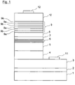
- FIG. 1 the layer sequence of a semiconductor layer structure of an optoelectronic component with a superlattice is shown schematically in cross section.
- an adaptation layer 2 and following an n-doped contact layer 3 are grown on a substrate 1.
- the doping type of layers will be given below by prefixing the letter n or p, eg, n-contact layer 3.
- n-contact layer 3 On the n-contact layer 3 there is an n-type cladding layer 4 and an n-type waveguide layer 5. An active layer 6 is applied to this, followed by a barrier layer 7 and a p-type waveguide layer 8. A p-type cladding layer follows which acts as a superlattice 9 is executed.
- the superlattice 9 has the alternately stacked layers 9a of a first type a and layers 9b of a second type b.
- a p-contact layer 10 is grown on the superlattice 9.
- the layer sequence is through Etching down to a surface facing away from the substrate of the n-contact layer 3, or was not built up in this area by masking.
- an n-contact 11 is applied on the exposed surface of the n-contact layer 3, an n-contact 11 is applied.
- On the p-contact layer 10 is a p-contact 12th
- FIG. 1 is to be understood as a schematic drawing. In particular, the layer thicknesses shown are not true to scale.
- This in FIG. 1 shown component represents a double heterostructure laser diode.
- sapphire can be used as the substrate 1
- n-type GaN can be used as the n-type contact layer 3.
- silicon (Si) is used for n-doping of the GaN layer.
- an aluminum nitride (AlN) layer is typically provided between the sapphire substrate 1 and the GaN n contact layer 3 for adapting the different lattice constants of this layer.
- the p-contact layer 10 can be realized by a GaN layer doped with magnesium (Mg), wherein a hole line induced by the magnesium perturbations is activated in a known manner after the layer has grown, for example by electron irradiation or thermal treatment.
- Mg magnesium
- electrodes for example made of aluminum or nickel, can be vapor-deposited onto the corresponding n- or p-contact layers 3 and 10, respectively.
- the necessary for the purpose exposing the n-contact layer 3 can for example, by a dry etching in chlorine gas or by argon ion sputtering done.
- a conductive substrate such as e.g. Gallium nitride (GaN) or silicon carbide (SiC) can be used.
- GaN Gallium nitride
- SiC silicon carbide
- the n-contact 11 can then be applied to the p-contact 12 on the side of the substrate facing away from the semiconductor layer structure, so that a vertically conductive semiconductor layer structure is formed.
- FIG. 1 an embodiment shown in the first n-doped layers are applied to the substrate 1.
- An arrangement in which p-doped layers are arranged closer to the substrate 1 than the n-doped layers is also possible.
- the two embodiments may have different properties with respect to the charge carrier injection into the semiconductor layer structure. Depending on the desired properties, each of the embodiments may prove advantageous in individual cases.
- the active layer 6 may e.g. a single or multiple quantum layer structure in which indium gallium nitride (InGaN) quantum layers are stacked alternately with AlGaN barrier layers.
- InGaN indium gallium nitride
- a quantum layer is to be understood as meaning a layer which is dimensioned or structured in such a way that a quantization of the charge carrier energy levels essential for the generation of radiation, for example by confinement.
- the term quantum layer does not include any indication or limitation about the dimensionality of the quantization.
- the quantum layer may form a two-dimensional quantum well or contain lower dimensional structural elements such as quantum wires or quantum dots, or combinations of these structures.
- the layers surrounding the active layer 6 (n- and p-waveguide layers 5 and 8, n-cladding layer 4, superlattice 9 as p-cladding layer and barrier layer 7) have a larger bandgap than the active layer 6. This causes a concentration or a
- the number of layers provided for this purpose is not limited to the number of five layers shown in the figure, but in principle arbitrary.
- the layers surrounding the active layer 6 form a waveguide for the radiation generated in the active layer 6.
- Good waveguiding properties are achieved when the refractive index in a direction perpendicular to the active layer 6 decreases outwardly therefrom.
- GaN has a higher refractive index than AlGaN
- the n and p waveguide layers 5 and 8 arranged closer to the active layer 6 are designed as GaN layers in the exemplary embodiment.
- the n-type cladding layer 4 and the superlattice 9 as the p-type cladding layer are preferably aluminum-containing.
- the waveguide layer 5 can be embodied, for example, as a Si-doped GaN layer and the cladding layer 4 as an Si-doped AlGaN layer.
- a magnesium (Mg) -doped GaN layer can be used analogously as waveguide layer 8.
- the barrier layer 7 is additionally provided between the two layers. This can be realized by a preferably highly p-doped AlGaN layer, which is typically made significantly thinner than the n- and p-waveguide layers 5 and 8, the n-cladding layer 4 or the superlattice 9.
- the p-side cladding layer is realized by the superlattice 9.
- the superlattice 9 is formed by alternately arranged layers 9a of the first type a and layers 9b of the second type b.
- the superlattice typically has a greater number of layers, for example, tens to hundreds of layers of each type.
- Typical layer thicknesses for a single layer of the superlattice 9 are in the range of a few nm to several tens of nm, for example between 2 nm and 50 nm and preferably between 3 nm and 10 nm.
- Layers of the same type exhibit nominal (ie within the accuracy of the film thickness control during or after the growth process) the same layer thickness.
- the layers 9a of the first type a and the layers 9b of the second type b may differ in their thickness (asymmetric superlattice) or be the same (symmetric superlattice).
- the superlattice 9 may be formed as a p-type cladding layer, e.g. consist of alternating Mg-doped GaN layers and Mg-doped AlGaN layers. Due to the high activation energy of the Mg doping atoms, the electrical conductivity of p-doped layers is low.
- AlGaN has a larger band gap than GaN and has lower conductivity due to lower doping efficiency.
- the doping efficiency indicates the concentration at which dopants are actually taken up by the material and which fraction of doped atoms taken up in principle (i.e., irrelevant to temperature-induced occupation effects) can at all contribute to the conductivity. The doping efficiency depends, inter alia, on which lattice or interstitial sites occupy the doping atoms.
- the superlattice 9 can have an increased conductivity with effectively the same refractive index compared with a p-doped pure AlGaN cladding layer.
- An effective same refractive index can be achieved by an increased aluminum content of the AlGaN layers used in the superlattice 9 compared with the pure AlGaN cladding layer.
- a superlattice 9 is also conceivable, are alternately stacked in the Al x Ga 1-x N / Al y Ga 1-y N layers with 0 ⁇ x, y ⁇ 1, and x ⁇ y , Also, the use of In instead of Al in all or some layers of the superlattice 9 is possible. Also, superlattices 9 are conceivable in which three or more different types of layers are alternately stacked.
- n-doped AlGaN cladding layer 4 is also conceivable for the n-doped AlGaN cladding layer 4.
- an advantage is not primarily in increased vertical conductivity. Advantages, however, result from a possible reduction of stresses which are induced in the active layer 6.
- Another advantage, which comes into play in particular with lateral current injection, is due to the increased lateral current conductivity of a superlattice.
- the superlattice 9 can, for example due to its content of Al, induce stresses in the active layer 6. Although these strains can be alleviated by the GaN waveguide layer 8 located between the superlattice 9 and the active layer 6, they are not necessarily sufficiently reduced. This is particularly true since the thickness of the GaN waveguide layer 8, on which a reduction of the induced stresses depends, is predetermined due to the requirements of the optical waveguide properties.
- the content of Al and also In, which also has effects on induced stresses in the active layer 6, within the layers of at least one type in the superlattice 9 is not constant, whereby the superlattice 9 in the best possible way to the contrary requirements of good waveguide and low induced strain can be adjusted.
- the content of at least one element in this case Al and / or In
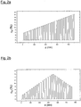
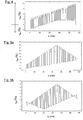
- FIGS. 2 to 5 Detailed descriptions of corresponding superlattices in which the content of at least one element (in this case Al and / or In) varies within layers of one or more types in the superlattice will be described below in connection with the embodiments and comparative examples FIGS. 2 to 5 given.
- FIGS. 2 to 5 In each case, in various embodiments and comparative examples of a superlattice, a respective diagram is shown in which the Al content c Al and optionally the In content c In in percent (ordinate) depending on a vertical position z within the superlattice of a semiconductor layer structure (Abscissa) is indicated. As the zero point of the vertical position z within the superlattice, the side of the superlattice facing an active layer is selected. The active layer thus lies to the left of the illustrated region of the superlattice at negative values of the vertical position z.
- FIG. 12 shows a superlattice of a semiconductor layer structure according to a comparative example, in which layers of two different types a, b are alternately stacked. Of each layer type a, b, 30 layers with a layer thickness of 7.5 nm each are provided, so that the superlattice is 450 nm thick in total.
- the layers of type a are GaN layers.
- the layers of type b are AlGaN layers, wherein the Al content c Al of these layers increases linearly from about 5% to 20% from layer to layer and wherein the Al content c Al is graded within the individual AlGaN layers. The average Al content of the AlGaN layers is thus 12.5%.
- the layer facing the active layer in this case has the lowest Al content c Al .
- the superlattice induces FIG. 2a less stress in the active layer, since the lattice structure and - constants in the superlattice change favorably with the falling down to the active layer Al content.
- An Al content which decreases towards the active layer may furthermore be preferred because transition barriers to the active layer are lowered and thus a heterostructure transition is less pronounced.
- a graded Al content within a layer can aid the conductivity-enhancing effect of a superlattice.
- an in-situ depth determination can take place via the relationship between Al content c Al of the layers in the superlattice and their position within the superlattice.
- a measurement of the Al content of the removed material can be carried out, for example, by mass spectrometry.
- FIG. 2b shows an embodiment of a GaN / AlGaN superlattice, in which the Al content c Al in the AlGaN layers inside the superlattice has a maximum value of about 17% and drops to both sides. In this way, stresses on both sides of the superlattice are reduced, wherein in the example shown the maximum value is not reached exactly in the middle of the superlattice and the layer closest to an active layer has a lower Al content c Al than that of the active layer on furthest removed layer.
- the course of the Al content c Al within a superlattice can be described by an (envelope) function which specifies the Al content c Al of a layer as a function of the position of the layer.
- an (envelope) function which specifies the Al content c Al of a layer as a function of the position of the layer.
- a common function for all types of layers a, b, etc. may be specified, or it may be given a separate function for each layer type.
- any desired, eg non-linear, function course is possible.
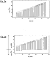
- FIG. 3 are comparative examples of superlattices of a semiconductor layer structure in which layers of three different types a, b and c are stacked alternately.
- the layers of type a are in the example of FIG. 3a GaN layers of constant composition over the superlattice.
- the layers of layer types b and c are AlGaN layers whose Al content c Al varies within the superlattice.
- the Al content c Al increases linearly with increasing vertical position z of the layer, however, a type c layer has 2% more Al than the layer directly adjacent to it of type b.
- layers of type b and c are only half as thick as layers of type a.
- the structure can also be considered as a GaN / AlGaN superlattice with only two types of layers, of which the AlGaN layers are graded with a step function.
- a graded Al content within a layer can aid the conductivity-increasing effect of a superlattice.
- the AlGaN layers of the type b and c are carried out as in the example of FIG. 3a , As layers of type a, however, InGaN layers with variable In content c In are provided.
- In the examples of FIG. 3b and 3c follows the In content c In a step function, in the first case with a constant In content within a layer, in the second case with a graded In content.
- the In content c In decreases linearly within 6 layers and is zero for the remaining layers.
- GaN layers can lead to a reduction of induced stress in the active layer, but on the other hand, deteriorate waveguiding by the superlattice, because a higher In content increases the refractive index of the superlattice, resulting in a lower refractive index contrast to an adjacent waveguide layer.
- the non-constant In content c In which is greater in the direction of the active layer, enhances the positive effects of InGaN layers in the superlattice over the adverse effects.
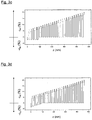
- FIG. 4 shows a comparative example of a superlattice of a semiconductor layer structure in which layers of four different types a, b, c and d are stacked alternately.
- the layers of c and d are similar to layers b and c FIG. 3 AlGaN layers whose Al content c Al linearly increases within the superlattice within the layers of one type, the Al content c Al of a type d layer being about 2% higher than that of the adjacent c type layer, respectively ,
- the In content c In ie the coefficient x, initially decreases linearly in the first 9 layers of the type a and the first 8 layers of the type b (calculated from an active layer) and is zero in the following layers.
- the Al content c Al ie the coefficient y, is zero in the first 8 or 9 layers (z between 0 and 130 nm), then increases linearly for the following middle layers (z between 130 and 270 nm), for the remaining layers (z> 270 nm) at a constant Level to stay.
- the structure can also be considered as a superlattice with only two types of layers, of which the AlGaN layers are graded with a step function.
- the advantages that have a low Al content c Al and an increased In content c In in layers that are directly or indirectly adjacent to the active layer with respect to induced strain are in this embodiment with the positive effects of a (gradual) graded Al content combined to the conductivity of the superlattice.
- FIG. 5 Exemplary embodiments of AlGaN / AlGaN superlattices of a semiconductor layer structure are shown.
- the layers of both types a and b are AlGaN layers in which the Al content c Al varies within the superlattice.
- the Al content c Al depending on the vertical position z of a layer of the type a is described by a first function
- the Al content c Al of a layer of the type b is given by a second function.
- the first function unlike the second.
- Directly adjacent layers thus differ in their Al content c Al and thus in their composition. However, this does not mean that a layer of type a can not have the same composition as a layer of type b.
- the first function is a function that increases linearly with the vertical position z.
- FIG. 5 is created by the varying in both types of layers a and b Al content c Al a superlattice, which allows a good waveguide by a high average Al content and yet by the falling to the active layer Al content c Al tensions on the active layer reasonably low.
Landscapes
- Engineering & Computer Science (AREA)
- Physics & Mathematics (AREA)
- Manufacturing & Machinery (AREA)
- Computer Hardware Design (AREA)
- Chemical & Material Sciences (AREA)
- Power Engineering (AREA)
- Optics & Photonics (AREA)
- Nanotechnology (AREA)
- Microelectronics & Electronic Packaging (AREA)
- Crystallography & Structural Chemistry (AREA)
- Life Sciences & Earth Sciences (AREA)
- Biophysics (AREA)
- Condensed Matter Physics & Semiconductors (AREA)
- General Physics & Mathematics (AREA)
- Electromagnetism (AREA)
- Led Devices (AREA)
- Semiconductor Lasers (AREA)
Description
Diese Patentanmeldung beansprucht die Priorität der deutschen Patentanmeldungen
Die Erfindung betrifft ein optoelektronisches Bauelement mit einer Halbleiter-Schichtstruktur, die ein Übergitter aus gestapelten Schichten eines ersten und mindestens eines zweiten Typs, wobei die Schichten des ersten Typs und des mindestens einen zweiten Typs III-V Verbindungshalbleiter sind und sich im Übergitter benachbarte Schichten unterschiedlichen Typs in der Zusammensetzung in mindestens einem Element unterscheiden.The invention relates to an optoelectronic component with a semiconductor layer structure, which is a superlattice of stacked layers of a first and at least one second type, wherein the layers of the first type and of the at least one second type III-V are compound semiconductors and differ in the superlattice adjacent layers Type in the composition differ in at least one element.
Verglichen mit einer Schicht gleicher Dicke aus nur einem Material einer Zusammensetzung haben Übergitter mit gestapelten Schichten verschiedenen Typs unterschiedliche elektrische, optische und epitaktische Eigenschaften. Insbesondere kann bei geeigneter Zusammensetzung und Dotierung ein Übergitter aus alternierend gestapelten p-dotierten Gallium-Nitrid- (GaN) und p-dotierten Aluminium-Gallium-Nitrid- (AlGaN) Schichten eine höhere Leitfähigkeit aufweisen als eine p-dotierte reine GaN- oder AlGaN-Schicht der gleichen Dicke. Aufgrund dieser Eigenschaften finden Übergitter vielfach Verwendung in elektronischen und optoelektronischen Bauteilen.Compared with a layer of the same thickness made of only one material of a composition, stacked layer superlattices of different types have different electrical, optical and epitaxial properties. In particular, with a suitable composition and doping, a superlattice of alternately stacked p-doped gallium nitride (GaN) and p-doped aluminum gallium nitride (AlGaN) layers may have a higher conductivity than a p-doped pure GaN or AlGaN Layer of the same thickness. Due to these properties, superlattices are frequently used in electronic and optoelectronic components.
Optoelektronische Bauelemente mit einer Halbleiter-Schichtstruktur, die ein Übergitter enthält, werden zum Beispiel in den Druckschriften
Aufgabe der Erfindung ist es, ein optoelektronisches Bauelement mit einer Halbleiter-Schichtstruktur mit Übergitter der eingangs genannten Art mit verbesserten elektrischen und optischen Eigenschaften zu schaffen.The object of the invention is to provide an optoelectronic component with a semiconductor layer structure with superlattice of the type mentioned with improved electrical and optical properties.
Diese Aufgabe wird gemäß Patentanspruch 1 durch ein optoelektronisches Bauelement gelöst, das eine aktive Schicht aufweist, wobei die aktive Schicht zwischen Wellenleiterschichten angeordnet ist, zwischen der aktiven Schicht und einer der Wellenleiterschichten eine Barriereschicht angeordnet ist, und jeweils auf der der aktiven Schicht abgewandten Seite der Wellenleiterschichten eine Mantelschicht angeordnet ist. Zumindest eine Mantelschicht umfasst eine Halbleiter-Schichtstruktur, die ein Übergitter aus gestapelten Schichten eines ersten und mindestens eines zweiten Typs umfasst, wobei die Schichten des ersten Typs und des mindestens einen zweiten Typs alternierend gestapelte InxAlyGa1-x-yN- und InwAlzGa1-w-zN-Schichten mit 0 ≤ x, y, w, z ≤ 1 und x + y ≤ 1 und w + z ≤ 1 sind. Im Übergitter unterscheiden sich benachbarte Schichten unterschiedlichen Typs in der Zusammensetzung in mindestens einem Element, wobei zumindest zwei Schichten eines gleichen Typs einen unterschiedlichen Gehalt an dem mindestens einen Element aufweisen. Der Gehalt an dem mindestens einen Element der Schichten zumindest eines Typs ist innerhalb des Übergitters gradiert. Die Schichten des Übergitters enthalten Dotierstoffe in vorgegebenen Konzentrationen, wobei das Übergitter Schichten aufweist, die mit Mg in unterschiedlichen Konzentrationen dotiert sind. Der Gehalt an dem mindestens einen Element im Inneren des Übergitters hat einen Maximalwert, der nicht in der Mitte des Übergitters liegt.This object is achieved according to
Auf diese Weise können die elektrischen, optischen und epitaktischen Eigenschaften des Übergitters bestmöglich an gegebene Erfordernisse angepasst werden. Dieses gilt insbesondere für epitaktische Randbedingungen, an die das Übergitter angepasst werden kann.In this way, the electrical, optical and epitaxial properties of the superlattice can best be adapted to given requirements. This applies in particular to epitaxial boundary conditions to which the superlattice can be adapted.
Häufig sind die gegebenen Erfordernisse an das Übergitter nicht über seine gesamte Dicke gleich, beispielsweise weil physikalische Größen, wie eine elektrische oder optische Feldstärke, die Einfluss auf die Erfordernisse haben, ebenfalls über die Dicke des Übergitters nicht konstant sind.Often, the given requirements for the superlattice are not the same throughout its thickness, for example, because physical quantities, such as electrical or optical field strength, that affect the requirements are also not constant across the thickness of the superlattice.
Beispielsweise kann die Zusammensetzung innerhalb der Schichten eines Typs sowohl Einfluss auf den Brechungsindex und damit auf eine optische Wellenführung, als auch auf die Größe der Bandlücke und damit auf optische Absorptionsverluste, als auch auf Gitterstruktur und/oder -konstante und damit auf Verspannungen, die das Übergitter auf angrenzende Schichten ausübt, haben. Dabei kann die Abhängigkeit der Größen von dem Gehalt an einem Element bezüglich gewünschter Eigenschaften des Übergitters beispielsweise derart gegenläufig sein, dass ein hoher Gehalt zwar die Wellenführung durch das Übergitter vorteilhaft beeinflusst und/oder optische Absorptionsverluste vorteilhaft verringert, aber auch Verspannungen angrenzender Schichten nachteilig verstärkt.For example, the composition within the layers of one type can affect both the refractive index and thus an optical waveguide, as well as the size of the band gap and thus optical absorption losses, as well as lattice structure and / or constant and thus to the stresses Has superlattices on adjacent layers. In this case, the dependence of the quantities on the content of an element with respect to desired properties of the superlattice can be countercurrent, for example, such that a high content advantageously influences the waveguide through the superlattice and / or advantageously reduces optical absorption losses, but also disadvantageously amplifies stresses of adjacent layers.
Eine gleiche Zusammensetzung für alle Schichten eines Typs kann in einem solchen Fall bestenfalls ein Kompromiss zwischen erreichbaren Vorteilen und in Kauf zu nehmenden Nachteilen darstellen. Durch die innerhalb eines Schichtentyps variierende Zusammensetzung, durch einen gradierten Gehalt an dem mindestens einem Element und durch unterschiedliche Dotierstoffe können räumlich unterschiedlichen Anforderungen an das Übergitter dagegen Rechnung getragen werden. Insbesondere wird für Schichten im Randbereich des Übergitters, die bezüglich der Verspannungen auf angrenzende Schichten maßgeblich sind, eine andere Zusammensetzung und/oder andere Dotierstoffe vorgesehen, als für Schichten im mittleren Bereich des Übergitters, die wegen der größeren räumlichen Ausdehnung des mittleren Bereichs für die Wellenführung maßgeblich sind.In such a case, a similar composition for all layers of one type can at best be a compromise between achievable advantages and to be accepted Represent disadvantages. By varying the composition within a layer type, by a graded content of the at least one element and by different dopants, however, spatially different requirements for the superlattice can be taken into account. In particular, for layers in the edge region of the superlattice which are relevant to the stresses on adjacent layers, a different composition and / or dopants are provided, as for layers in the central region of the superlattice, due to the greater spatial extent of the central region for the waveguide are relevant.
Grundsätzlich wird als Übergitter eine Struktur bezeichnet, die eine Periodizität aufweist, deren Periodenlänge größer ist als die Gitterkonstanten eingesetzter Materialien. Im Rahmen der Anmeldung wird als Übergitter eine Folge gestapelter Schichten bezeichnet, bei der sich in einer Richtung senkrecht zu den Grenzflächen zwischen den Schichten, also z.B. in Aufwachsrichtung der Schichten, eine Schichtabfolge, umfassend mindestens zwei Schichten unterschiedlichen Typs, wiederholt. Ein Übergitter in diesem Sinne ist beispielsweise durch eine Folge alternierend gestapelter Schichten verschiedener Typen gegeben, wobei alternierend so zu verstehen ist, dass sich zwei oder mehr Schichten abwechseln. Innerhalb der sich wiederholenden Schichtabfolge kann dabei ein Typ durch mehr als eine Schicht vertreten sein. Beispiele für derartige Übergitter sind durch die folgenden Schichtenfolgen gegeben: "ab|ab|ab|...", "abc|abc|abc|...", "abcb|abcb|..." und "ababababc|ababababc|...", wobei a, b und c jeweils Schichten eines Typs angeben und die sich wiederholende Schichtenabfolge durch das Trennzeichen "|" verdeutlicht ist.In principle, the superlattice is a structure which has a periodicity whose period length is greater than the lattice constants of the materials used. In the context of the application, the superlattice is a sequence of stacked layers in which a sequence of layers comprising at least two layers of different types is repeated in a direction perpendicular to the boundary surfaces between the layers, ie, in the growth direction of the layers. A superlattice in this sense is given, for example, by a series of alternately stacked layers of different types, wherein alternately it is to be understood that two or more layers alternate. Within the repeating layer sequence, a type can be represented by more than one layer. Examples of such superlattices are given by the following layer sequences: "ab | ab | ab | ...", "abc | abc | abc | ...", "abcb | abcb | ..." and "ababababc | ababababc | ... ", where a, b and c respectively denote layers of one type and the repeating layer sequence by the separator" | " is clarified.
Im Rahmen der Anmeldung ist die Zusammensetzung einer Schicht durch in der Schicht enthaltene Elemente sowie ihre nominelle (d.h. im Rahmen der Genauigkeit der Kompositionsüberwachung während oder nach dem Wachstumsprozess) Stöchiometrie definiert, wobei Dotierstoffe und Verunreinigungen nicht mitberücksichtigt werden. Die Stöchiometrie ist durch den Gehalt (Anteil) der einzelnen Elemente in der Schicht gegeben.In the context of the application, the composition of a layer is defined by elements contained in the layer as well as their nominal (i.e., within the accuracy of composition monitoring during or after the growth process) stoichiometry, which does not take into account dopants and impurities. The stoichiometry is given by the content (proportion) of the individual elements in the layer.
Der Typ einer Schicht ist durch die Zusammensetzung der Schicht gegeben, wobei das jedoch nicht zwangsläufig bedeutet, dass alle Schichten eines Typs die gleiche Zusammensetzung aufweisen. Die Zusammensetzung der Schichten eines Typs kann innerhalb des Übergitters in vorgegebener Weise variieren, z.B. indem die Konzentration eines Elements der Schichten eines Typs von Schicht zu Schicht dieses Typs anwächst. Im Übergitter benachbarte Schichten unterschiedlichen Typs unterscheiden sich jedoch in ihrer Zusammensetzung in mindestens einem Element.The type of layer is given by the composition of the layer, but this does not necessarily mean that all layers of one type have the same composition. The composition of the layers of one type may vary within the superlattice in a predetermined manner, e.g. by increasing the concentration of an element of the layers of one type from layer to layer of this type. However, adjacent layers of different types in the superlattice differ in composition in at least one element.
Bei der Halbleiter-Schichtstruktur weist das Übergitter alternierend gestapelte InxAlyGa1-x-yN- und InwAlzGa1-w-zN-Schichten mit 0≤x,y,w,z<1 und x+y≤1 und w+z≤1 auf. Dieses Materialsystem ist zum einen von großer technologischer Bedeutung und zum anderen kann in diesem System eine vorteilhafte Leitfähigkeitserhöhung insbesondere der Löcherleitung durch den Einsatz eines Übergitters beobachtet werden.In the semiconductor layer structure, the superlattice has alternately stacked In x Al y Ga 1-xy N and In w Al z Ga 1 -wz N layers with 0 ≦ x, y, w, z <1 and x + y ≦ 1 and w + z≤1. On the one hand, this material system is of great technological importance and, on the other hand, in this system an advantageous increase in conductivity, in particular of the hole line, can be observed through the use of a superlattice.
Gemäß einer weiteren vorteilhaften Ausgestaltung der Halbleiter-Schichtstruktur ist den einzelnen Schichten des Übergitters eine vertikale Position innerhalb der Halbleiter-Schichtstruktur zugeordnet und der Gehalt an dem mindestens einen Element in einer Schicht ist in vorgegebener Weise abhängig von ihrer vertikalen Position innerhalb der Halbleiter-Schichtstruktur. Auf diese Weise kann das Übergitter und seine Eigenschaften bestmöglich an räumlich unterschiedliche Anforderungen an das Übergitter angepasst werden.According to a further advantageous embodiment of the semiconductor layer structure, the individual layers of the superlattice are assigned a vertical position within the semiconductor layer structure and the content of the at least one element in a layer is dependent on their vertical position within the semiconductor layer structure in a predetermined manner. In this way, the superlattice and its properties can best be adapted to spatially different requirements of the superlattice.
Gemäß weiterer vorteilhafter Ausgestaltungen ist die Abhängigkeit des Gehalts an dem mindestens einen Element von der vertikalen Position entweder für alle Schichten durch eine gemeinsame Funktion vorgegeben oder sie ist für Schichten des ersten Typs durch eine erste Funktion und für Schichten des zweiten Typs durch mindestens eine zweite Funktion vorgegeben. Besonders bevorzugt ist dabei die erste und/oder die mindestens eine zweite und/oder die gemeinsame Funktion eine Stufenfunktion oder eine monoton steigende/fallende Funktion oder eine lineare Funktion oder eine Polynomfunktion oder eine Wurzelfunktion oder eine exponentielle Funktion oder eine logarithmische Funktion oder eine periodische Funktion oder eine Superposition der genannten Funktion oder enthält Anteile einer dieser Funktionen.According to further advantageous embodiments, the dependence of the content on the at least one element from the vertical position is given either for all layers by a common function or it is for layers of the first type by a first function and for layers of the second type by at least one second function specified. In this case, the first and / or the at least one second and / or common function is particularly preferably a step function or a monotonically increasing / decreasing function or a linear function or a polynomial function or a root function or an exponential function or a logarithmic function or a periodic function or a superposition of said function or contains portions of one of these functions.
Gemäß einer weiteren vorteilhaften Ausgestaltungen weisen alle Schichten des Übergitters eine gleiche Dicke auf. Gemäß einer weiteren vorteilhaften Ausgestaltungen weisen Schichten unterschiedlichen Typs unterschiedliche Dicken auf.According to a further advantageous embodiment, all layers of the superlattice have the same thickness. According to a further advantageous embodiment, layers of different types have different thicknesses.
Gemäß vorteilhafter Ausgestaltungen des optoelektronischen Bauelements istdas mindestens eine Element, dessen Gehalt in zumindest zwei Schichten des gleichen Typs unterschiedlich ist, Al. Dabei steigt der Al-Gehalt innerhalb des Übergitters der Halbleiter-Schichtstruktur mit wachsendem Abstand von der optisch aktiven Schicht an oder fällt ab. Bei einem optoelektronischen Bauelement mit optisch aktiver Schicht kann ein hoher Al-Gehalt einer unmittelbar oder mittelbar an die aktive Schicht angrenzenden Schicht des Übergitters zu nachteiligen Verspannungen in der aktiven Schicht führen, durch die die Quanteneffizienz dieser Schicht verringert wird. Durch einen zur aktiven Schicht hin abfallenden Al-Gehalt innerhalb des Übergitters können Verluste durch eine geringere Quanteneffizienz verringert werden. Ein höherer Al-Gehalt führt dagegen zu einer größeren Bandlücke und damit zu einer geringeren optischen Absorption einer Schicht. Da in Richtung der aktiven Schicht die Intensität einer von der aktiven Schicht erzeugten Strahlung ansteigt, kann ein zur aktiven Schicht hin ansteigender Al-Gehalt innerhalb des Übergitters folglich bezüglich optischer Absorptionsverluste vorteilhaft sein.According to advantageous embodiments of the optoelectronic component, the at least one element whose content is different in at least two layers of the same type is Al. In this case, the Al content within the superlattice of the semiconductor layer structure increases or decreases with increasing distance from the optically active layer. In an optoelectronic component having an optically active layer, a high Al content of a layer of the superlattice directly or indirectly adjacent to the active layer can lead to disadvantageous stresses in the active layer, which reduce the quantum efficiency of this layer. By decreasing the Al content within the superlattice to the active layer, losses due to lower quantum efficiency can be reduced. In contrast, a higher Al content leads to a larger band gap and thus to a lower optical absorption of a layer. Since the intensity of a radiation generated by the active layer increases in the direction of the active layer, an Al content within the superlattice which increases towards the active layer can consequently be advantageous with respect to optical absorption losses.
Gemäß weiterer vorteilhafter Ausgestaltungen ist das optoelektronische Bauelement eine Leuchtdiode oder eine Laserdiode.According to further advantageous embodiments, the optoelectronic component is a light-emitting diode or a laser diode.
Weitere vorteilhafte Ausgestaltungen der Erfindung ergeben sich aus den im folgenden in Verbindung mit den in den Figuren beschriebenen Ausführungs- und Vergleichsbeispielen.Further advantageous embodiments of the invention will become apparent from the following in connection with the embodiments and comparative examples described in the figures.
Es zeigen:
Figur 1- eine Querschnittszeichnung eines optoelektronischen Bauelements mit einer erfindungsgemäßen Halbleiter-Schichtstruktur mit Übergitter und die
- Figuren 2-5
- schematische Darstellungen des Gehalts eines oder verschiedener Elemente abhängig von einer vertikalen Position in einem Übergitter bei verschiedenen Ausführungs- und Vergleichsbeispielen einer Halbleiter-Schichtstruktur mit Übergitter.
- FIG. 1
- a cross-sectional drawing of an optoelectronic component having a semiconductor layer structure according to the invention with superlattice and the
- Figures 2-5
- schematically represent the content of one or several elements depending on a vertical position in a superlattice in various embodiments and comparative examples of a semiconductor layer structure with superlattice.
In
Auf der n-Kontaktschicht 3 befindet sich eine n-Mantelschicht 4 und eine n-Wellenleiterschicht 5. Auf diese ist eine aktive Schicht 6 aufgebracht, anschließend eine Barriereschicht 7 sowie eine p-Wellenleiterschicht 8. Es folgt eine p-Mantelschicht, die als Übergitter 9 ausgeführt ist. Das Übergitter 9 weist die alternierend gestapelten Schichten 9a eines ersten Typs a und Schichten 9b eines zweiten Typs b auf.On the n-
Auf das Übergitter 9 ist eine p-Kontaktschicht 10 aufgewachsen. Im rechten Bereich ist die Schichtenfolge durch Abätzen bis auf eine dem Substrat abgewandte Fläche der n-Kontaktschicht 3 abgetragen, beziehungsweise wurde in diesem Bereich durch Maskierung erst gar nicht aufgebaut. Auf der freiliegenden Fläche der n-Kontaktschicht 3 ist ein n-Kontakt 11 aufgebracht. Auf der p-Kontaktschicht 10 befindet sich ein p-Kontakt 12.On the superlattice 9, a p-
Die
Das in
Analog kann die p-Kontaktschicht 10 durch eine mit Magnesium (Mg) p-dotierte GaN-Schicht realisiert werden, wobei eine durch die Magnesiumstörstellen induzierte Löcherleitung nach Aufwachsen der Schicht in bekannter Weise aktiviert wird, z.B. durch Elektronenbestrahlung oder thermische Behandlung. Als n- oder p-Kontakte 11 bzw. 12 können Elektroden, z.B. aus Aluminium oder Nickel, auf die entsprechenden n- oder p-Kontaktschichten 3 bzw. 10 aufgedampft werden. Das zu dem Zweck erforderliche Freilegen der n-Kontaktschicht 3 kann beispielsweise durch einen Trockenätzprozess in Chlorgas oder durch Argon-Ionen-Sputtern erfolgen.Analogously, the p-
Alternativ kann statt eines nicht leitenden Substrats 1 ein leitendes Substrat, wie z.B. Galliumnitrid (GaN) oder Siliziumkarbid (SiC), eingesetzt werden. In einem solchen Fall kann die n-Kontaktschicht 3 und gegebenenfalls, z.B. beim Einsatz von GaN, die Anpassungsschicht 2 entfallen. Der n-Kontakt 11 kann dann gegenüber dem p-Kontakt 12 auf der der Halbleiter-Schichtstruktur abgewandten Seite des Substrats aufgebracht werden, so dass eine vertikal leitende Halbleiter-Schichtstruktur gebildet wird.Alternatively, instead of a
Ohne Einschränkung ist in der
Die aktive Schicht 6 kann z.B. eine Einfach- oder Mehrfach-Quantenschichtstruktur sein, bei der Indium-Galliumnitrid (InGaN)-Quantenschichten abwechselnd mit AlGaN-Barriereschichten gestapelt sind.The
Als Quantenschicht ist im Rahmen der Erfindung eine Schicht zu verstehen, die so dimensioniert oder strukturiert ist, dass eine für die Strahlungserzeugung wesentliche Quantisierung der Ladungsträger-Energieniveaus, zum Beispiel durch Einschluss (confinement), auftritt. Insbesondere beinhaltet die Bezeichnung Quantenschicht keine Angabe oder Einschränkung über die Dimensionalität der Quantisierung. Die Quantenschicht kann einen zweidimensionalen Quantentopf bilden oder strukturelle Elemente mit niedrigerer Dimensionalität wie Quantendrähte oder Quantenpunkte oder Kombinationen dieser Strukturen enthalten.Within the scope of the invention, a quantum layer is to be understood as meaning a layer which is dimensioned or structured in such a way that a quantization of the charge carrier energy levels essential for the generation of radiation, for example by confinement. In particular, the term quantum layer does not include any indication or limitation about the dimensionality of the quantization. The quantum layer may form a two-dimensional quantum well or contain lower dimensional structural elements such as quantum wires or quantum dots, or combinations of these structures.
Darüber hinaus ist auch der Einsatz einer Fotolumineszenzaktiven Schicht, z. B. einer Fremdatom-dotierten InGaN-Schicht als aktive Schicht 6 denkbar.In addition, the use of a photoluminescent active layer, for. As an impurity-doped
Die die aktive Schicht 6 umgebenden Schichten (n- und p-Wellenleiterschichten 5 bzw. 8, n-Mantelschicht 4, Übergitter 9 als p-Mantelschicht und Barriereschicht 7) haben eine größere Bandlücke als die aktiven Schicht 6. Dieses bewirkt eine Konzentration oder eine Eingrenzung, auch confinement genannt, von Ladungsträgern und/oder Feldern auf die aktive Schicht 6. Die Anzahl der zu diesem Zweck vorgesehenen Schichten ist nicht auf die in der Figur gezeigte Anzahl von fünf Schichten festgelegt, sondern prinzipiell beliebig.The layers surrounding the active layer 6 (n- and p-
Weiterhin bilden die die aktive Schicht 6 umgebenden Schichten einen Wellenleiter für die in der aktiven Schicht 6 erzeugte Strahlung. Gute Wellenführungseigenschaften werden erreicht, wenn der Brechungsindex in einer Richtung senkrecht zur aktiven Schicht 6 von dieser aus nach außen abnimmt. Da GaN einen höheren Brechungsindex aufweist als AlGaN, sind die näher an der aktiven Schicht 6 angeordneten n- und p-Wellenleiterschichten 5 bzw. 8 im Ausführungsbeispiel als GaN-Schichten ausgeführt. Die n-Mantelschicht 4 und das Übergitter 9 als p-Mantelschicht sind bevorzugt aluminiumhaltig.Furthermore, the layers surrounding the
Auf der dem Substrat 1 zugewandten Seite der aktiven Schicht 6 (n-dotierte Seite) kann die Wellenleiterschicht 5 beispielsweise als eine Si-dotierte GaN-Schicht ausgeführt sein und die Mantelschicht 4 als eine Si-dotierte AlGaN-Schicht. Auf der dem Substrat 1 abgewandten Seite der aktiven Schicht 6 (p-dotierte Seite) kann analog eine Magnesium (Mg)-dotierte GaN-Schicht als Wellenleiterschicht 8 eingesetzt werden. Um eine direkte Rekombination von Elektronen, die aus der aktiven Schicht 6 in die Wellenleiterschicht 8 diffundieren, mit den dort befindlichen Löchern zu verhindern, ist zwischen beiden Schichten zusätzlich die Barriereschicht 7 vorgesehen. Diese kann durch eine bevorzugt hoch p-dotierte AlGaN-Schicht realisiert sein, die typischerweise deutlich dünner als die n- und p-Wellenleiterschichten 5 bzw. 8, die n-Mantelschicht 4 oder das Übergitter 9 ausgeführt ist.On the side of the active layer 6 (n-doped side) facing the
Die p-seitige Mantelschicht wird durch das Übergitter 9 realisiert.The p-side cladding layer is realized by the superlattice 9.
Im Ausführungsbeispiel der
Im GaN-basierten Materialsystem kann das Übergitter 9 als p-Mantelschicht z.B. aus alternierenden Mg-dotierten GaN-Schichten und Mg-dotierten AlGaN-Schichten bestehen. Aufgrund der hohen Aktivierungsenergie der Mg-Dotieratome ist die elektrische Leitfähigkeit von p-dotierten Schichten gering. Zudem hat AlGaN eine größere Bandlücke als GaN und weist aufgrund einer geringeren Dotiereffizienz eine geringere Leitfähigkeit auf. Die Dotiereffizienz gibt an, in welcher Konzentration Dotierstoffe überhaupt vom Material aufgenommen werden und welcher Anteil aufgenommener Dotieratome prinzipiell (d.h. unbeachtlich temperaturbedingter Besetzungseffekte) überhaupt zur Leitfähigkeit beitragen kann. Die Dotiereffizienz ist unter anderem davon abhängig, welche Gitter- oder Zwischengitterplätze die Dotieratome einnehmen.In the GaN-based material system, the superlattice 9 may be formed as a p-type cladding layer, e.g. consist of alternating Mg-doped GaN layers and Mg-doped AlGaN layers. Due to the high activation energy of the Mg doping atoms, the electrical conductivity of p-doped layers is low. In addition, AlGaN has a larger band gap than GaN and has lower conductivity due to lower doping efficiency. The doping efficiency indicates the concentration at which dopants are actually taken up by the material and which fraction of doped atoms taken up in principle (i.e., irrelevant to temperature-induced occupation effects) can at all contribute to the conductivity. The doping efficiency depends, inter alia, on which lattice or interstitial sites occupy the doping atoms.
Durch den Einsatz höher und effizienter dotierbarer und somit leitfähigerer GaN-Schichten kann das Übergitter 9 verglichen mit einer p-dotierten reinen AlGaN-Mantelschicht eine erhöhte Leitfähigkeit bei effektiv gleichem Brechungsindex aufweisen.By using higher and more efficiently dopable and thus more conductive GaN layers, the superlattice 9 can have an increased conductivity with effectively the same refractive index compared with a p-doped pure AlGaN cladding layer.
Ein effektiv gleicher Brechungsindex kann durch einen erhöhten Aluminiumgehalt der im Übergitter 9 eingesetzten AlGaN-Schichten verglichen mit der reinen AlGaN-Mantelschicht erreicht werden.An effective same refractive index can be achieved by an increased aluminum content of the AlGaN layers used in the superlattice 9 compared with the pure AlGaN cladding layer.
Statt eines GaN-/AlGaN-Übergitters 9 ist ebenso ein Übergitter 9 denkbar, in dem AlxGa1-xN/AlyGa1-yN-Schichten mit 0≤x,y≤1 und x≠y abwechselnd gestapelt sind. Ebenfalls ist der Einsatz von In statt Al in allen oder einigen Schichten des Übergitters 9 möglich. Auch sind Übergitter 9 denkbar, bei denen drei oder mehr verschiedenen Schichttypen alternierend gestapelt sind.Instead of a GaN / AlGaN superlattice 9 is a superlattice 9 is also conceivable, are alternately stacked in the Al x Ga 1-x N / Al y Ga 1-y N layers with 0 ≦ x, y ≦ 1, and x ≠ y , Also, the use of In instead of Al in all or some layers of the superlattice 9 is possible. Also, superlattices 9 are conceivable in which three or more different types of layers are alternately stacked.
Weiterhin ist auch für die n-dotierte AlGaN-Mantelschicht 4 der Einsatz eines Übergitters denkbar. Aufgrund der im Allgemeinen höheren Leitfähigkeit von n-dotierten Schichten liegt in diesem Fall ein Vorteil nicht primär in einer erhöhten vertikalen Leitfähigkeit. Vorteile ergeben sich jedoch durch eine mögliche Verringerung von Verspannungen, die in der aktiven Schicht 6 induziert werden. Ein weiterer Vorteil, der insbesondere bei seitlicher Stromeinbringung zum Tragen kommt, liegt in der erhöhten lateralen Stromleitfähigkeit eines Übergitters begründet.Furthermore, the use of a superlattice is also conceivable for the n-doped
Das Übergitter 9 kann, z.B. aufgrund seines Gehalts an Al, Verspannungen in der aktiven Schicht 6 induzieren. Diese Verspannungen können durch die zwischen dem Übergitter 9 und der aktiven Schicht 6 liegende GaN-Wellenleiterschicht 8 zwar abgemindert werden, jedoch nicht unbedingt in ausreichendem Maße. Dieses gilt insbesondere, da die Dicke der GaN-Wellenleiterschicht 8, von der eine Verringerung der induzierten Verspannungen abhängt, aufgrund der Anforderungen an die optischen Wellenleitereigenschaften vorgegeben ist.The superlattice 9 can, for example due to its content of Al, induce stresses in the
Erfindungsgemäß ist der Gehalt an Al und auch In, das ebenfalls Auswirkungen auf induzierte Verspannungen in der aktiven Schicht 6 hat, innerhalb der Schichten zumindest einen Typs im Übergitter 9 nicht konstant, wodurch das Übergitter 9 in bestmöglicher Weise an die gegenläufigen Anforderungen von guter Wellenleitung und geringer induzierter Verspannung angepasst werden kann. Detaillierte Beschreibungen von entsprechenden Übergittern, bei denen der Gehalt an zumindest einem Element (hier Al und/oder In) innerhalb Schichten einer oder mehrerer Typen im Übergitters variiert, werden im Folgenden im Zusammenhang mit den Ausführungs- und Vergleichsbeispielen der
In den
Das Übergitter wird jeweils durch eine Vielzahl alternierend gestapelter Schichten verschiedener Typen a, b und ggf. auch c, d gebildet, wobei per Definition die bei z=0 beginnende, der aktiven Schicht am nächsten liegende Schicht des Übergitters vom Typ a sei.The superlattice is formed in each case by a multiplicity of alternately stacked layers of different types a, b and optionally also c, d, wherein by definition the layer of the superlattice closest to the active layer beginning at z = 0 is of type a.
In
Ein weiterer Vorteil eines Übergitters, bei dem der Al-Gehalt cAl sich linear oder, allgemeiner, umkehrbar eindeutig mit der Position einer Schicht im Übergitter verändert, ergibt sich im Herstellungsprozess eines Bauelements. Zur Aufbringung von Kontakten oder zur Wellenführung ist häufig das Einbringen von Gräben (ridges) in eine Halbleiterstruktur erforderlich. Um eine definierte Tiefe der Gräben sicherzustellen, wird in manchen Materialsystemen nasschemisches Ätzen in Verbindung mit so genannten Ätzstoppschichten eingesetzt. Beim dem gegenüber nasschemischen Ätzprozessen resistenten AlGaN-Materialsystem kann jedoch üblicherweise nur das wenig material-selektive Trockenätzen benutzt werden. Wenn während des Ätzprozesses der Al-Gehalt des abgetragenen Materials gemessen wird, kann über den Zusammenhang zwischen Al-Gehalt cAl der Schichten im Übergitter und deren Position innerhalb des Übergitters eine in-situ Tiefenbestimmung erfolgen. Eine Messung des Al-Gehalt des abgetragenen Materials kann beispielsweise massenspektometrisch erfolgen.Another advantage of a superlattice in which the Al content c Al changes linearly or, more generally, reversibly, unambiguously with the position of a layer in the superlattice results in the manufacturing process of a component. For the application of contacts or waveguide often the introduction of ridges in a semiconductor structure is required. To a defined depth of the trenches In some material systems, wet-chemical etching is used in conjunction with so-called etch stop layers. In the case of the AlGaN material system which is resistant to wet-chemical etching processes, however, only the less material-selective dry etching can usually be used. If the Al content of the removed material is measured during the etching process, an in-situ depth determination can take place via the relationship between Al content c Al of the layers in the superlattice and their position within the superlattice. A measurement of the Al content of the removed material can be carried out, for example, by mass spectrometry.
Verallgemeinert kann der Verlauf des Al-Gehalts cAl innerhalb eines Übergitters durch eine (Hüllkurven-) Funktion beschrieben werden, die den Al-Gehalt cAl einer Schicht abhängig von der Position der Schicht angibt. Dabei kann entweder eine gemeinsame Funktion für alle Schichtentypen a, b, usw. vorgegeben sein, oder es kann für jeden Schichtentyp eine eigene Funktion vorgegeben sein. Prinzipiell ist dabei jeder beliebige, z.B. auch nichtlineare, Funktionsverlauf möglich.In general, the course of the Al content c Al within a superlattice can be described by an (envelope) function which specifies the Al content c Al of a layer as a function of the position of the layer. In this case, either a common function for all types of layers a, b, etc. may be specified, or it may be given a separate function for each layer type. In principle, any desired, eg non-linear, function course is possible.
In
Die Schichten vom Typ a sind im Beispiel von
Bei den in den
In
Im Beispiel in
Bei den Ausführungsbeispielen der
Claims (12)
- Optoelectronic component comprising an active layer (6), wherein- the active layer (6) is arranged between waveguide layers (5, 8),- a barrier layer (7) is arranged between the active layer (6) and one of the waveguide layers (8),- a cladding layer is arranged in each case on that side of the waveguide layers which faces away from the active layer, at least one cladding layer comprises a semiconductor layer structure comprising a superlattice (9) composed of stacked layers (9a, 9b) of a first type (a) and at least one second type (b),- the layers (9a, 9b) of the first type (a) and of the at least one second type (b) are alternately stacked InxAlyGa1-x-yN and InwAlzGa1-w-zN layers where 0 ≤ x, y, w, z ≤ 1 and x + y ≤ 1 and w + z ≤ 1,- in the superlattice (9) adjacent layers of different types differ in at least one element in the composition,- in the superlattice (9) at least two layers of an identical type have a different content (cAl, cIn) of the at least one element,- the content (cAl, cIn) of the at least one element of the layers (9a, 9b) of at least one type (a, b) is graded within the superlattice (9),- the layers (9a, 9b) of the superlattice (9) contain dopants in predefined concentrations, wherein the superlattice (9) comprises layers (9a, 9b) which are doped with Mg in different concentrations, and- the content (cAl, cIn) of the at least one element internally in the superlattice has a maximum value that does not lie in the centre of the superlattice.
- Optoelectronic component according to Claim 1, wherein individual layers of the superlattice (9) are assigned a vertical position z within the semiconductor layer structure, and the content (cAl, cIn) of the at least one element in a layer is dependent on the vertical position (z) thereof within the semiconductor layer structure in a predefined manner.
- Optoelectronic component according to Claim 2, wherein the dependence of the content (cAl, cIn) of the at least one element on the vertical position (z) is predefined by a common function for all layers (9a, 9b) of the superlattice (9).
- Optoelectronic component according to Claim 2, wherein the dependence of the content (cAl, cIn) of the at least one element on the vertical position (z) is predefined by a first function for layers (9a) of the first type (a) and by at least one second function for layers (9b) of the at least one second type (b).
- Optoelectronic component according to Claim 4, wherein the first function is a step function or a monotonically rising/falling function or a linear function or a polynomial function or an exponential function or a logarithmic function or a periodic function or a superposition of the stated functions or contains portions of one of these functions.
- Optoelectronic component according to either of Claims 4 and 5, wherein the at least one second function is a step function or a monotonically rising/falling function or a linear function or a polynomial function or an exponential function or a logarithmic function or a periodic function or a superposition of the stated functions or contains portions of one of these functions.
- Optoelectronic component according to Claim 3, wherein the common function is a step function or a monotonically rising/falling function or a linear function or a polynomial function or an exponential function or a logarithmic function or a periodic function or a superposition of the stated functions or contains portions of one of these functions.
- Optoelectronic component according to any of Claims 1 to 7, wherein the content (cAl, cIn) of the at least one element is constant within a layer (9a, 9b) of the superlattice (9).
- Optoelectronic component according to any of Claims 1 to 8, wherein all the layers (9a, 9b) have identical thicknesses.
- Optoelectronic component according to any of Claims 1 to 8, wherein layers (9a, 9b) of different types (a, b) have different thicknesses.
- Optoelectronic component according to any of the preceding claims, which is a light-emitting diode.
- Optoelectronic component according to any of the preceding claims 1 to 10, which is a laser diode.
Applications Claiming Priority (2)
| Application Number | Priority Date | Filing Date | Title |
|---|---|---|---|
| DE102006034820 | 2006-07-27 | ||
| DE102006046237A DE102006046237A1 (en) | 2006-07-27 | 2006-09-29 | Semiconductor-layer structure useful in optoelectronic component, comprises a super lattice out of alternating piled layers of a first and a second type |
Publications (2)
| Publication Number | Publication Date |
|---|---|
| EP1883141A1 EP1883141A1 (en) | 2008-01-30 |
| EP1883141B1 true EP1883141B1 (en) | 2017-05-24 |
Family
ID=38542049
Family Applications (1)
| Application Number | Title | Priority Date | Filing Date |
|---|---|---|---|
| EP07013822.7A Expired - Fee Related EP1883141B1 (en) | 2006-07-27 | 2007-07-13 | LD or LED with superlattice cladding layer |
Country Status (3)
| Country | Link |
|---|---|
| US (2) | US7893424B2 (en) |
| EP (1) | EP1883141B1 (en) |
| JP (1) | JP2008034851A (en) |
Families Citing this family (49)
| Publication number | Priority date | Publication date | Assignee | Title |
|---|---|---|---|---|
| US20060039498A1 (en) * | 2004-08-19 | 2006-02-23 | De Figueiredo Rui J P | Pre-distorter for orthogonal frequency division multiplexing systems and method of operating the same |
| EP1883119B1 (en) | 2006-07-27 | 2015-11-04 | OSRAM Opto Semiconductors GmbH | Semiconductor layer structure with overlay grid |
| EP1883141B1 (en) | 2006-07-27 | 2017-05-24 | OSRAM Opto Semiconductors GmbH | LD or LED with superlattice cladding layer |
| EP1883140B1 (en) | 2006-07-27 | 2013-02-27 | OSRAM Opto Semiconductors GmbH | LD or LED with superlattice clad layer and graded doping |
| WO2009120990A2 (en) * | 2008-03-27 | 2009-10-01 | Nitek, Inc. | Ultraviolet light emitting diode/laser diode with nested superlattice |
| DE102008030584A1 (en) * | 2008-06-27 | 2009-12-31 | Osram Opto Semiconductors Gmbh | Method for producing an optoelectronic component and optoelectronic component |
| JP5167081B2 (en) * | 2008-11-13 | 2013-03-21 | パナソニック株式会社 | Nitride semiconductor devices |
| DE102009037416B4 (en) | 2009-08-13 | 2021-10-14 | OSRAM Opto Semiconductors Gesellschaft mit beschränkter Haftung | Electrically pumped optoelectronic semiconductor chip |
| JP5743893B2 (en) * | 2009-09-28 | 2015-07-01 | 株式会社トクヤマ | Manufacturing method of laminate |
| US8389977B2 (en) | 2009-12-10 | 2013-03-05 | Transphorm Inc. | Reverse side engineered III-nitride devices |
| KR101422452B1 (en) | 2009-12-21 | 2014-07-22 | 가부시끼가이샤 도시바 | Nitride semiconductor light-emitting element and method for manufacturing same |
| DE102009060749B4 (en) | 2009-12-30 | 2021-12-30 | OSRAM Opto Semiconductors Gesellschaft mit beschränkter Haftung | Optoelectronic semiconductor chip |
| FR2957718B1 (en) * | 2010-03-16 | 2012-04-20 | Commissariat Energie Atomique | HYBRID HIGH PERFORMANCE ELECTROLUMINESCENT DIODE |
| US8742460B2 (en) | 2010-12-15 | 2014-06-03 | Transphorm Inc. | Transistors with isolation regions |
| US8643062B2 (en) | 2011-02-02 | 2014-02-04 | Transphorm Inc. | III-N device structures and methods |
| US8358673B2 (en) * | 2011-02-17 | 2013-01-22 | Corning Incorporated | Strain balanced laser diode |
| US20130329760A1 (en) * | 2011-02-28 | 2013-12-12 | Corning Incorporated | Semiconductor lasers with indium containing cladding layers |
| US8901604B2 (en) | 2011-09-06 | 2014-12-02 | Transphorm Inc. | Semiconductor devices with guard rings |
| US9257547B2 (en) | 2011-09-13 | 2016-02-09 | Transphorm Inc. | III-N device structures having a non-insulating substrate |
| US8598937B2 (en) | 2011-10-07 | 2013-12-03 | Transphorm Inc. | High power semiconductor electronic components with increased reliability |
| KR20130079873A (en) * | 2012-01-03 | 2013-07-11 | 엘지이노텍 주식회사 | Light emitting device and lighting system including the same |
| CN102544281A (en) * | 2012-01-20 | 2012-07-04 | 厦门市三安光电科技有限公司 | Gallium nitride-based LED with multi-layer potential barrier structure |
| US9165766B2 (en) | 2012-02-03 | 2015-10-20 | Transphorm Inc. | Buffer layer structures suited for III-nitride devices with foreign substrates |
| US9093366B2 (en) | 2012-04-09 | 2015-07-28 | Transphorm Inc. | N-polar III-nitride transistors |
| US9219189B2 (en) | 2012-09-14 | 2015-12-22 | Palo Alto Research Center Incorporated | Graded electron blocking layer |
| US9401452B2 (en) | 2012-09-14 | 2016-07-26 | Palo Alto Research Center Incorporated | P-side layers for short wavelength light emitters |
| KR101936312B1 (en) | 2012-10-09 | 2019-01-08 | 엘지이노텍 주식회사 | Light emitting device |
| KR102042181B1 (en) * | 2012-10-22 | 2019-11-07 | 엘지이노텍 주식회사 | Light emitting device |
| JP2014143338A (en) * | 2013-01-25 | 2014-08-07 | Sharp Corp | Nitride semiconductor light-emitting element |
| US9087718B2 (en) | 2013-03-13 | 2015-07-21 | Transphorm Inc. | Enhancement-mode III-nitride devices |
| US9245992B2 (en) | 2013-03-15 | 2016-01-26 | Transphorm Inc. | Carbon doping semiconductor devices |
| KR20140117117A (en) * | 2013-03-26 | 2014-10-07 | 인텔렉추얼디스커버리 주식회사 | Nitride semiconductor light emitting device |
| WO2015009514A1 (en) | 2013-07-19 | 2015-01-22 | Transphorm Inc. | Iii-nitride transistor including a p-type depleting layer |
| US9318593B2 (en) | 2014-07-21 | 2016-04-19 | Transphorm Inc. | Forming enhancement mode III-nitride devices |
| KR102237111B1 (en) * | 2014-07-28 | 2021-04-08 | 엘지이노텍 주식회사 | Light emitting device and lighting system |
| FR3028670B1 (en) * | 2014-11-18 | 2017-12-22 | Commissariat Energie Atomique | SEMICONDUCTOR SEMICONDUCTOR LAYER STRUCTURE OF GROUP III-V OR II-VI COMPRISING CRYSTALLINE STRUCTURE WITH CUBIC OR HEXAGONAL MESH |
| US9536967B2 (en) | 2014-12-16 | 2017-01-03 | Transphorm Inc. | Recessed ohmic contacts in a III-N device |
| US9536966B2 (en) | 2014-12-16 | 2017-01-03 | Transphorm Inc. | Gate structures for III-N devices |
| TWI577046B (en) * | 2014-12-23 | 2017-04-01 | 錼創科技股份有限公司 | Semiconductor light-emitting device and manufacturing method thereof |
| US9673352B2 (en) * | 2015-04-30 | 2017-06-06 | National Chiao Tung University | Semiconductor light emitting device |
| JP6888013B2 (en) | 2016-01-15 | 2021-06-16 | トランスフォーム テクノロジー,インコーポレーテッド | Enhancement Mode Group III Nitride Devices with AL (1-x) Si (x) O-Gate Insulators |
| TWI813243B (en) | 2016-05-31 | 2023-08-21 | 美商創世舫科技有限公司 | Iii-nitride devices including a graded depleting layer |
| DE102017119931A1 (en) * | 2017-08-30 | 2019-02-28 | Osram Opto Semiconductors Gmbh | Optoelectronic semiconductor component |
| US20190103509A1 (en) | 2017-09-30 | 2019-04-04 | Sensor Electronic Technology, Inc. | Semiconductor Heterostructure with P-type Superlattice |
| US10516076B2 (en) | 2018-02-01 | 2019-12-24 | Silanna UV Technologies Pte Ltd | Dislocation filter for semiconductor devices |
| US10879420B2 (en) | 2018-07-09 | 2020-12-29 | University Of Iowa Research Foundation | Cascaded superlattice LED system |
| CN110600591B (en) * | 2019-08-21 | 2021-11-26 | 苏州紫灿科技有限公司 | Deep ultraviolet LED with chirp superlattice final potential barrier structure and preparation method thereof |
| US20220368108A1 (en) * | 2019-09-30 | 2022-11-17 | Nlight, Inc. | Strain-engineered cladding layer for optimized active region strain and improved laser diode performance |
| US11322647B2 (en) | 2020-05-01 | 2022-05-03 | Silanna UV Technologies Pte Ltd | Buried contact layer for UV emitting device |
Family Cites Families (75)
| Publication number | Priority date | Publication date | Assignee | Title |
|---|---|---|---|---|
| JPS60145686A (en) | 1984-01-09 | 1985-08-01 | Nec Corp | Semiconductor laser |
| US4882734A (en) | 1988-03-09 | 1989-11-21 | Xerox Corporation | Quantum well heterostructure lasers with low current density threshold and higher TO values |
| US4839899A (en) * | 1988-03-09 | 1989-06-13 | Xerox Corporation | Wavelength tuning of multiple quantum well (MQW) heterostructure lasers |
| JPH01241192A (en) | 1988-03-23 | 1989-09-26 | Fujitsu Ltd | Semiconductor device |
| US4961197A (en) | 1988-09-07 | 1990-10-02 | Hitachi, Ltd. | Semiconductor laser device |
| CA1299719C (en) | 1989-01-13 | 1992-04-28 | Hui Chun Liu | Semiconductor superlattice infrared source |
| US5060028A (en) | 1989-01-19 | 1991-10-22 | Hewlett-Packard Company | High band-gap opto-electronic device |
| US4984242A (en) * | 1989-09-18 | 1991-01-08 | Spectra Diode Laboratories, Inc. | GaAs/AlGaAs heterostructure laser containing indium |
| US5319657A (en) | 1991-10-08 | 1994-06-07 | Matsushita Electric Industrial Co., Ltd. | Semiconductor laser of modulation doping quantum well structure with stopper against dopant dispersion and manufacturing method thereof |
| US5198682A (en) | 1991-11-12 | 1993-03-30 | Hughes Aircraft Company | Multiple quantum well superlattice infrared detector with graded conductive band |
| JPH0794829A (en) | 1993-04-05 | 1995-04-07 | Matsushita Electric Ind Co Ltd | Semiconductor laser |
| US5395793A (en) | 1993-12-23 | 1995-03-07 | National Research Council Of Canada | Method of bandgap tuning of semiconductor quantum well structures |
| US5570386A (en) | 1994-04-04 | 1996-10-29 | Lucent Technologies Inc. | Semiconductor laser |
| US5497012A (en) | 1994-06-15 | 1996-03-05 | Hewlett-Packard Company | Unipolar band minima devices |
| KR100290076B1 (en) | 1994-07-21 | 2001-06-01 | 모리시타 요이찌 | Semiconductor light emitting device and manufacturing method thereof |
| US5670798A (en) | 1995-03-29 | 1997-09-23 | North Carolina State University | Integrated heterostructures of Group III-V nitride semiconductor materials including epitaxial ohmic contact non-nitride buffer layer and methods of fabricating same |
| US5588015A (en) | 1995-08-22 | 1996-12-24 | University Of Houston | Light emitting devices based on interband transitions in type-II quantum well heterostructures |
| JPH1022524A (en) | 1996-07-02 | 1998-01-23 | Omron Corp | Semiconductor light emitting device |
| US5936989A (en) | 1997-04-29 | 1999-08-10 | Lucent Technologies, Inc. | Quantum cascade laser |
| KR100660152B1 (en) | 1997-01-09 | 2006-12-21 | 니치아 카가쿠 고교 가부시키가이샤 | Nitride Semiconductor Device |
| US6677619B1 (en) | 1997-01-09 | 2004-01-13 | Nichia Chemical Industries, Ltd. | Nitride semiconductor device |
| JP3282175B2 (en) * | 1997-02-04 | 2002-05-13 | 日亜化学工業株式会社 | Nitride semiconductor device |
| JP3014339B2 (en) | 1997-04-25 | 2000-02-28 | カナレ電気株式会社 | Semiconductor device having quantum wave interference layer |
| JP3642157B2 (en) | 1997-05-26 | 2005-04-27 | ソニー株式会社 | P-type group III nitride compound semiconductor, light-emitting diode, and semiconductor laser |
| EP1014455B1 (en) | 1997-07-25 | 2006-07-12 | Nichia Corporation | Nitride semiconductor device |
| JPH1168158A (en) | 1997-08-20 | 1999-03-09 | Sanyo Electric Co Ltd | Gallium nitride based compound semiconductor device |
| JP3468082B2 (en) | 1998-02-26 | 2003-11-17 | 日亜化学工業株式会社 | Nitride semiconductor device |
| JPH11340505A (en) * | 1998-05-25 | 1999-12-10 | Matsushita Electric Ind Co Ltd | Gallium nitride-based compound semiconductor light emitting element |
| JP2000091708A (en) | 1998-09-14 | 2000-03-31 | Toshiba Corp | Semiconductor light emitting element |
| JP2000286451A (en) | 1998-11-17 | 2000-10-13 | Nichia Chem Ind Ltd | Nitride semiconductor device |
| JP2000244070A (en) | 1999-02-19 | 2000-09-08 | Sony Corp | Semiconductor device and semiconductor light-emitting element |
| EP1183761A2 (en) | 1999-03-26 | 2002-03-06 | Matsushita Electronics Corporation | Semiconductor structures having a strain compensated layer and method of fabrication |
| GB9913950D0 (en) | 1999-06-15 | 1999-08-18 | Arima Optoelectronics Corp | Unipolar light emitting devices based on iii-nitride semiconductor superlattices |
| DE19955747A1 (en) * | 1999-11-19 | 2001-05-23 | Osram Opto Semiconductors Gmbh | Optical semiconductor device with multiple quantum well structure, e.g. LED, has alternate well layers and barrier layers forming super-lattices |
| US6441393B2 (en) | 1999-11-17 | 2002-08-27 | Lumileds Lighting U.S., Llc | Semiconductor devices with selectively doped III-V nitride layers |
| JP2001168385A (en) | 1999-12-06 | 2001-06-22 | Toyoda Gosei Co Ltd | Iii nitride compound semiconductor element and iii nitride compound semiconductor light emitting element |
| US6535536B2 (en) | 2000-04-10 | 2003-03-18 | Fuji Photo Film Co., Ltd. | Semiconductor laser element |
| JP2002057410A (en) * | 2000-05-29 | 2002-02-22 | Fuji Photo Film Co Ltd | Semiconductor laser element |
| US6556604B1 (en) | 2000-11-08 | 2003-04-29 | Lucent Technologies Inc. | Flat minibands with spatially symmetric wavefunctions in intersubband superlattice light emitters |
| JP3453558B2 (en) | 2000-12-25 | 2003-10-06 | 松下電器産業株式会社 | Nitride semiconductor device |
| DE60230602D1 (en) | 2001-03-28 | 2009-02-12 | Nichia Corp | NITRIDE SEMICONDUCTOR ELEMENT |
| US6489636B1 (en) * | 2001-03-29 | 2002-12-03 | Lumileds Lighting U.S., Llc | Indium gallium nitride smoothing structures for III-nitride devices |
| US6649942B2 (en) | 2001-05-23 | 2003-11-18 | Sanyo Electric Co., Ltd. | Nitride-based semiconductor light-emitting device |
| US6630692B2 (en) | 2001-05-29 | 2003-10-07 | Lumileds Lighting U.S., Llc | III-Nitride light emitting devices with low driving voltage |
| US7692182B2 (en) | 2001-05-30 | 2010-04-06 | Cree, Inc. | Group III nitride based quantum well light emitting device structures with an indium containing capping structure |
| US6958497B2 (en) | 2001-05-30 | 2005-10-25 | Cree, Inc. | Group III nitride based light emitting diode structures with a quantum well and superlattice, group III nitride based quantum well structures and group III nitride based superlattice structures |
| JP2003008058A (en) | 2001-06-18 | 2003-01-10 | Showa Denko Kk | AlGaInP EPITAXIAL WAFER, METHOD OF MANUFACTURING THE SAME, AND SEMICONDUCTOR LIGHT-EMITTING ELEMENT USING THE SAME |
| JP4057802B2 (en) | 2001-09-05 | 2008-03-05 | 株式会社日立製作所 | Semiconductor optical device |
| JP2003273473A (en) | 2001-11-05 | 2003-09-26 | Nichia Chem Ind Ltd | Semiconductor element |
| US6618413B2 (en) | 2001-12-21 | 2003-09-09 | Xerox Corporation | Graded semiconductor layers for reducing threshold voltage for a nitride-based laser diode structure |
| US7919791B2 (en) | 2002-03-25 | 2011-04-05 | Cree, Inc. | Doped group III-V nitride materials, and microelectronic devices and device precursor structures comprising same |
| GB0207307D0 (en) | 2002-03-27 | 2002-05-08 | Koninkl Philips Electronics Nv | In-pixel memory for display devices |
| US7177336B2 (en) * | 2002-04-04 | 2007-02-13 | Sharp Kabushiki Kaisha | Semiconductor laser device |
| JP4119158B2 (en) | 2002-04-23 | 2008-07-16 | 三菱電機株式会社 | Semiconductor light emitting device using tilted multiple quantum barrier |
| JP3755084B2 (en) | 2002-04-24 | 2006-03-15 | 中東産業株式会社 | hinge |
| JP4221697B2 (en) | 2002-06-17 | 2009-02-12 | 日本電気株式会社 | Semiconductor device |
| US20030235224A1 (en) | 2002-06-19 | 2003-12-25 | Ohlander Ulf Roald | Strained quantum-well structure having ternary-alloy material in both quantum-well layers and barrier layers |
| US20060139743A1 (en) | 2002-11-20 | 2006-06-29 | Marsh John H | Semiconductor optical device with beam focusing |
| GB0306279D0 (en) | 2003-03-19 | 2003-04-23 | Bookham Technology Plc | High power semiconductor laser with large optical superlattice waveguide |
| WO2005006506A1 (en) * | 2003-07-10 | 2005-01-20 | Nichia Corporation | Nitride semiconductor laser element |
| KR100580623B1 (en) | 2003-08-04 | 2006-05-16 | 삼성전자주식회사 | Semiconductor device having super lattice semiconductor layer and manufacturing method thereof |
| TWI228320B (en) | 2003-09-09 | 2005-02-21 | Ind Tech Res Inst | An avalanche photo-detector(APD) with high saturation power, high gain-bandwidth product |
| EP1670106A4 (en) | 2003-09-25 | 2007-12-12 | Matsushita Electric Ind Co Ltd | Nitride semiconductor device and method for manufacturing same |
| US20050162616A1 (en) * | 2004-01-23 | 2005-07-28 | Hewlett-Packard Co. | System and method of contrast enhancement in digital projectors |
| DE102004009531B4 (en) | 2004-02-20 | 2007-03-01 | Forschungszentrum Rossendorf E.V. | Quantum cascade laser structure |
| US7294868B2 (en) | 2004-06-25 | 2007-11-13 | Finisar Corporation | Super lattice tunnel junctions |
| KR100662191B1 (en) | 2004-12-23 | 2006-12-27 | 엘지이노텍 주식회사 | Nitride semiconductor LED and fabrication method thereof |
| US7885306B2 (en) * | 2006-06-30 | 2011-02-08 | Osram Opto Semiconductors Gmbh | Edge-emitting semiconductor laser chip |
| EP1883140B1 (en) | 2006-07-27 | 2013-02-27 | OSRAM Opto Semiconductors GmbH | LD or LED with superlattice clad layer and graded doping |
| DE102006046237A1 (en) | 2006-07-27 | 2008-01-31 | Osram Opto Semiconductors Gmbh | Semiconductor-layer structure useful in optoelectronic component, comprises a super lattice out of alternating piled layers of a first and a second type |
| DE102006046228A1 (en) * | 2006-07-27 | 2008-01-31 | Osram Opto Semiconductors Gmbh | Semiconductor layer structure for optoelectronic component e.g. LED and laser diode, has stacked layers of two types comprising layer thicknesses that are increased with increased distance of active layers by layer to layer |
| EP1883119B1 (en) * | 2006-07-27 | 2015-11-04 | OSRAM Opto Semiconductors GmbH | Semiconductor layer structure with overlay grid |
| EP1883141B1 (en) * | 2006-07-27 | 2017-05-24 | OSRAM Opto Semiconductors GmbH | LD or LED with superlattice cladding layer |
| US7547908B2 (en) * | 2006-12-22 | 2009-06-16 | Philips Lumilieds Lighting Co, Llc | III-nitride light emitting devices grown on templates to reduce strain |
| DE102010009457A1 (en) * | 2010-02-26 | 2011-09-01 | Osram Opto Semiconductors Gmbh | Optoelectronic semiconductor chip |
-
2007
- 2007-07-13 EP EP07013822.7A patent/EP1883141B1/en not_active Expired - Fee Related
- 2007-07-20 US US11/780,514 patent/US7893424B2/en not_active Expired - Fee Related
- 2007-07-27 JP JP2007195432A patent/JP2008034851A/en active Pending
-
2011
- 2011-01-19 US US13/009,422 patent/US8471240B2/en active Active
Also Published As
| Publication number | Publication date |
|---|---|
| US7893424B2 (en) | 2011-02-22 |
| EP1883141A1 (en) | 2008-01-30 |
| US8471240B2 (en) | 2013-06-25 |
| US20110168977A1 (en) | 2011-07-14 |
| JP2008034851A (en) | 2008-02-14 |
| US20080054247A1 (en) | 2008-03-06 |
Similar Documents
| Publication | Publication Date | Title |
|---|---|---|
| EP1883141B1 (en) | LD or LED with superlattice cladding layer | |
| EP1883140B1 (en) | LD or LED with superlattice clad layer and graded doping | |
| EP2212931B1 (en) | Led having current spreading layer | |
| EP2165374B1 (en) | Radiation-emitting semiconductor body | |
| EP2208240B1 (en) | Optoelectronic semiconductor chip having a multiple quantum well structure | |
| EP2519980B1 (en) | Light-emitting semiconductor chip | |
| WO2018050466A1 (en) | Semiconductor layer sequence | |
| WO2009036730A2 (en) | Opto-electronic semiconductor chip having quantum well structure | |
| DE102011112706A1 (en) | Optoelectronic component | |
| EP1883119B1 (en) | Semiconductor layer structure with overlay grid | |
| DE102006046237A1 (en) | Semiconductor-layer structure useful in optoelectronic component, comprises a super lattice out of alternating piled layers of a first and a second type | |
| WO2016110433A1 (en) | Optoelectronic component | |
| DE102012220911A1 (en) | Semiconductor laser with improved current conduction | |
| DE102013017275B4 (en) | Optoelectronic semiconductor component | |
| EP2465148B1 (en) | Electrically pumped optoelectronic semiconductor chip | |
| DE102016109022A1 (en) | laser diode chip | |
| WO2010012256A1 (en) | Optoelectronic semiconductor chip | |
| EP2478601A2 (en) | Edge-emitting semiconductor laser | |
| EP3345224B1 (en) | Optoelectronic semiconductor chip and method for producing same | |
| WO2010048918A1 (en) | Optoelectronic semiconductor chip and method for producing an optoelectronic semiconductor chip | |
| DE102006046227A1 (en) | Semiconductor layer structure has super lattice with alternative stacked layers of connecting semiconductors of one composition and another composition, where stacked layers have doping agents in specific concentration | |
| DE112018005379B4 (en) | Laser diode | |
| WO2021013740A1 (en) | Optoelectronic semiconductor chip | |
| DE102006046228A1 (en) | Semiconductor layer structure for optoelectronic component e.g. LED and laser diode, has stacked layers of two types comprising layer thicknesses that are increased with increased distance of active layers by layer to layer | |
| EP2457296B1 (en) | Optoelectronic semiconductor body with a quantum well |
Legal Events
| Date | Code | Title | Description |
|---|---|---|---|
| PUAI | Public reference made under article 153(3) epc to a published international application that has entered the european phase |
Free format text: ORIGINAL CODE: 0009012 |
|
| AK | Designated contracting states |
Kind code of ref document: A1 Designated state(s): AT BE BG CH CY CZ DE DK EE ES FI FR GB GR HU IE IS IT LI LT LU LV MC MT NL PL PT RO SE SI SK TR |
|
| AX | Request for extension of the european patent |
Extension state: AL BA HR MK YU |
|
| RAP1 | Party data changed (applicant data changed or rights of an application transferred) |
Owner name: OSRAM OPTO SEMICONDUCTORS GMBH |
|
| RAP1 | Party data changed (applicant data changed or rights of an application transferred) |
Owner name: OSRAM OPTO SEMICONDUCTORS GMBH |
|
| 17P | Request for examination filed |
Effective date: 20080707 |
|
| 17Q | First examination report despatched |
Effective date: 20080822 |
|
| AKX | Designation fees paid |
Designated state(s): DE |
|
| GRAP | Despatch of communication of intention to grant a patent |
Free format text: ORIGINAL CODE: EPIDOSNIGR1 |
|
| RIC1 | Information provided on ipc code assigned before grant |
Ipc: H01S 5/32 20060101ALN20161013BHEP Ipc: H01L 33/32 20100101ALI20161013BHEP Ipc: H01S 5/20 20060101ALN20161013BHEP Ipc: H01S 5/343 20060101AFI20161013BHEP Ipc: H01L 33/04 20100101ALN20161013BHEP Ipc: H01S 5/042 20060101ALN20161013BHEP Ipc: H01L 33/06 20100101ALI20161013BHEP Ipc: H01S 5/30 20060101ALN20161013BHEP |
|
| RIC1 | Information provided on ipc code assigned before grant |
Ipc: H01L 33/06 20100101ALI20161019BHEP Ipc: H01S 5/30 20060101ALN20161019BHEP Ipc: H01S 5/042 20060101ALN20161019BHEP Ipc: H01L 33/32 20100101ALI20161019BHEP Ipc: H01S 5/343 20060101AFI20161019BHEP Ipc: H01L 33/04 20100101ALN20161019BHEP Ipc: H01S 5/20 20060101ALN20161019BHEP Ipc: H01S 5/32 20060101ALN20161019BHEP |
|
| INTG | Intention to grant announced |
Effective date: 20161104 |
|
| RIN1 | Information on inventor provided before grant (corrected) |
Inventor name: LELL, ALFRED Inventor name: SCHILLGALIES, MARC Inventor name: EICHLER, CHRISTOPH Inventor name: MILER, ANDREAS |
|
| GRAS | Grant fee paid |
Free format text: ORIGINAL CODE: EPIDOSNIGR3 |
|
| RIN1 | Information on inventor provided before grant (corrected) |
Inventor name: EICHLER, CHRISTOPH Inventor name: SCHILLGALIES, MARC Inventor name: LELL, ALFRED Inventor name: MILER, ANDREAS |
|
| GRAA | (expected) grant |
Free format text: ORIGINAL CODE: 0009210 |
|
| AK | Designated contracting states |
Kind code of ref document: B1 Designated state(s): DE |
|
| REG | Reference to a national code |
Ref country code: DE Ref legal event code: R096 Ref document number: 502007015661 Country of ref document: DE |
|
| REG | Reference to a national code |
Ref country code: DE Ref legal event code: R097 Ref document number: 502007015661 Country of ref document: DE |
|
| PLBE | No opposition filed within time limit |
Free format text: ORIGINAL CODE: 0009261 |
|
| STAA | Information on the status of an ep patent application or granted ep patent |
Free format text: STATUS: NO OPPOSITION FILED WITHIN TIME LIMIT |
|
| 26N | No opposition filed |
Effective date: 20180227 |
|
| PGFP | Annual fee paid to national office [announced via postgrant information from national office to epo] |
Ref country code: DE Payment date: 20210721 Year of fee payment: 15 |
|
| REG | Reference to a national code |
Ref country code: DE Ref legal event code: R119 Ref document number: 502007015661 Country of ref document: DE |
|
| PG25 | Lapsed in a contracting state [announced via postgrant information from national office to epo] |
Ref country code: DE Free format text: LAPSE BECAUSE OF NON-PAYMENT OF DUE FEES Effective date: 20230201 |