EP1878584A2 - Multi-layer body with micro optics - Google Patents
Multi-layer body with micro optics Download PDFInfo
- Publication number
- EP1878584A2 EP1878584A2 EP07013569A EP07013569A EP1878584A2 EP 1878584 A2 EP1878584 A2 EP 1878584A2 EP 07013569 A EP07013569 A EP 07013569A EP 07013569 A EP07013569 A EP 07013569A EP 1878584 A2 EP1878584 A2 EP 1878584A2
- Authority
- EP
- European Patent Office
- Prior art keywords
- optical
- multilayer body
- layer
- micro
- body according
- Prior art date
- Legal status (The legal status is an assumption and is not a legal conclusion. Google has not performed a legal analysis and makes no representation as to the accuracy of the status listed.)
- Granted
Links
- 230000003287 optical effect Effects 0.000 claims abstract description 57
- 238000007639 printing Methods 0.000 claims abstract description 36
- 238000000034 method Methods 0.000 claims abstract description 32
- 230000000694 effects Effects 0.000 claims abstract description 21
- 239000010410 layer Substances 0.000 claims description 67
- 239000004922 lacquer Substances 0.000 claims description 28
- 239000011241 protective layer Substances 0.000 claims description 11
- 238000004519 manufacturing process Methods 0.000 claims description 7
- 239000002105 nanoparticle Substances 0.000 claims description 7
- 239000002184 metal Substances 0.000 claims description 5
- 229910052751 metal Inorganic materials 0.000 claims description 5
- 239000011248 coating agent Substances 0.000 claims description 4
- 238000000576 coating method Methods 0.000 claims description 4
- 238000003825 pressing Methods 0.000 claims description 3
- 150000002739 metals Chemical class 0.000 claims description 2
- 150000003839 salts Chemical class 0.000 claims description 2
- 229910001092 metal group alloy Inorganic materials 0.000 claims 1
- 239000002245 particle Substances 0.000 claims 1
- 239000000758 substrate Substances 0.000 description 16
- 239000003973 paint Substances 0.000 description 12
- 238000007646 gravure printing Methods 0.000 description 8
- 238000010030 laminating Methods 0.000 description 7
- 239000012790 adhesive layer Substances 0.000 description 6
- 239000000976 ink Substances 0.000 description 6
- 238000003475 lamination Methods 0.000 description 6
- 239000000463 material Substances 0.000 description 6
- 238000003491 array Methods 0.000 description 4
- 229920000642 polymer Polymers 0.000 description 3
- 230000015572 biosynthetic process Effects 0.000 description 2
- 238000011109 contamination Methods 0.000 description 2
- 238000004049 embossing Methods 0.000 description 2
- 239000011159 matrix material Substances 0.000 description 2
- 230000000737 periodic effect Effects 0.000 description 2
- 230000010363 phase shift Effects 0.000 description 2
- 239000004033 plastic Substances 0.000 description 2
- 238000002310 reflectometry Methods 0.000 description 2
- 239000002966 varnish Substances 0.000 description 2
- 239000004831 Hot glue Substances 0.000 description 1
- 238000005299 abrasion Methods 0.000 description 1
- 239000013078 crystal Substances 0.000 description 1
- 239000011888 foil Substances 0.000 description 1
- 239000005338 frosted glass Substances 0.000 description 1
- 239000011521 glass Substances 0.000 description 1
- PCHJSUWPFVWCPO-UHFFFAOYSA-N gold Chemical compound [Au] PCHJSUWPFVWCPO-UHFFFAOYSA-N 0.000 description 1
- 239000010931 gold Substances 0.000 description 1
- 229910052737 gold Inorganic materials 0.000 description 1
- 238000001093 holography Methods 0.000 description 1
- 238000010348 incorporation Methods 0.000 description 1
- 239000004973 liquid crystal related substance Substances 0.000 description 1
- 230000007774 longterm Effects 0.000 description 1
- 238000001465 metallisation Methods 0.000 description 1
- 239000002114 nanocomposite Substances 0.000 description 1
- 239000000049 pigment Substances 0.000 description 1
- 239000002985 plastic film Substances 0.000 description 1
- 229920006255 plastic film Polymers 0.000 description 1
- 230000003252 repetitive effect Effects 0.000 description 1
- 238000007650 screen-printing Methods 0.000 description 1
Images

Classifications
-
- B—PERFORMING OPERATIONS; TRANSPORTING
- B42—BOOKBINDING; ALBUMS; FILES; SPECIAL PRINTED MATTER
- B42D—BOOKS; BOOK COVERS; LOOSE LEAVES; PRINTED MATTER CHARACTERISED BY IDENTIFICATION OR SECURITY FEATURES; PRINTED MATTER OF SPECIAL FORMAT OR STYLE NOT OTHERWISE PROVIDED FOR; DEVICES FOR USE THEREWITH AND NOT OTHERWISE PROVIDED FOR; MOVABLE-STRIP WRITING OR READING APPARATUS
- B42D25/00—Information-bearing cards or sheet-like structures characterised by identification or security features; Manufacture thereof
- B42D25/40—Manufacture
- B42D25/405—Marking
- B42D25/43—Marking by removal of material
-
- B—PERFORMING OPERATIONS; TRANSPORTING
- B41—PRINTING; LINING MACHINES; TYPEWRITERS; STAMPS
- B41M—PRINTING, DUPLICATING, MARKING, OR COPYING PROCESSES; COLOUR PRINTING
- B41M1/00—Inking and printing with a printer's forme
- B41M1/10—Intaglio printing ; Gravure printing
-
- B—PERFORMING OPERATIONS; TRANSPORTING
- B41—PRINTING; LINING MACHINES; TYPEWRITERS; STAMPS
- B41M—PRINTING, DUPLICATING, MARKING, OR COPYING PROCESSES; COLOUR PRINTING
- B41M3/00—Printing processes to produce particular kinds of printed work, e.g. patterns
- B41M3/14—Security printing
-
- B—PERFORMING OPERATIONS; TRANSPORTING
- B42—BOOKBINDING; ALBUMS; FILES; SPECIAL PRINTED MATTER
- B42D—BOOKS; BOOK COVERS; LOOSE LEAVES; PRINTED MATTER CHARACTERISED BY IDENTIFICATION OR SECURITY FEATURES; PRINTED MATTER OF SPECIAL FORMAT OR STYLE NOT OTHERWISE PROVIDED FOR; DEVICES FOR USE THEREWITH AND NOT OTHERWISE PROVIDED FOR; MOVABLE-STRIP WRITING OR READING APPARATUS
- B42D25/00—Information-bearing cards or sheet-like structures characterised by identification or security features; Manufacture thereof
- B42D25/40—Manufacture
- B42D25/45—Associating two or more layers
-
- B42D2035/44—
Definitions
- the invention relates to a method for producing a multilayer body having microoptical structures, to a multilayer body produced by the method, and to a security document having said multilayer body.
- micromirror array which is transferable to a paper or plastic substrate by printing with ink or lacquer.
- the period of the micromirrors is typically 30 to 60 ⁇ m.
- the micromirrors can be used both in transmitted and reflected light. In this way, a two-channel tilting image can be formed.
- the invention is based on the object, a simple and inexpensive method for producing a multilayer body with micro-optical structures, to be listed in the register for other security features, such as OVDs and pictorial representations, as well as such a multilayer body.
- the object of the invention is achieved by a method for producing a multilayer body having a first layer formed from microoptical structures, which at least partially covers one or more further layers, the image areas and / or effect areas, which form an optical effect in that the micro-optical structures are applied by intaglio printing to the layer lying below the first layer or introduced into the first layer.
- the object is further achieved by a multilayer body having a first layer formed from micro-optical structures, which at least partially covers one or more further layers, the image areas and / or effect areas, which form an optical effect, wherein it is provided that the micro-optical structures are applied by intaglio printing on the underlying layer of the first layer or incorporated in the first layer.
- the object is further achieved by a security document with the multilayer body according to the invention.
- the invention provides to apply micro-optical structures, such as microlens arrays or Blazegitter, by intaglio printing.
- the multilayer body may be both a transfer film applied to a security document or the security document itself or a security document with transfer film.
- micro-optical structure applied in an endless, repetitive pattern on the multilayer body or in the Multi-layer body is introduced without standing in the register to other micro-optical structures.
- the multilayer body according to the invention is characterized in that micro-optical structures can be produced which are not molded into a film layer. This avoids all the problems that can arise when microoptical structures are transferred in a roll-to-roll process into a transfer film and subsequently transferred to other security features in the register for other features. Another advantage is that a micro-optic structure formed of interconnected optical elements can not be removed and transferred without destroying the structure.
- the arrangement of the micro-optical structures in the register further increases the security against forgery of the multilayer body according to the invention.
- the multi-layer body may have a particularly strict register, because the effort to adjust the individual matched objects arises only once.
- micro-optical structures and the image areas and / or effect areas are applied by gravure printing.
- the image areas may, for example, be monochrome or multicolor images, such as alphanumeric characters, logos or the like.
- the effect areas may, for example, be OVDs, such as a hologram, KINEGRAM®, blaze grid or the like.
- the effect areas can also be tactile detectable effect areas, which, for example, make the value imprint of a bank note tangible in a suitable form. Tactile detectable areas may further provide protection against abrasion and / or contamination to other areas.
- optical effects for example colored imprints, in particular by means of effect pigments
- the register accuracy achieved with the method according to the invention can be achieved later only with great effort, so that the proposed method has a very high security against counterfeiting. It is also not possible to procure individual components and to unify them, because individual components, such as transfer films or the like, do not physically exist. Further advantages result from the fact that the microoptical structures and / or the image areas and / or the effect areas can at least partially overlap one another, as a result of which the security against counterfeiting is further increased.
- an optical paint is transferred by intaglio printing on the other layers.
- a layer formed from the optical lacquer is applied to the further layers and then the microoptical structures are molded into the layer formed from the optical lacquer by pressing on an intaglio printing plate which is at least partially color-free.
- the gravure plate at least partially as To use stamp and to press the gravure plate under high pressure on the layer formed from the optical paint, so that the optical paint completely filled in the surface of the gravure plate wells and thus the surface profile of the intaglio plate is molded into the lacquer layer. It is therefore provided in this embodiment, without printing ink.
- a large number of paints are available for the process according to the invention, for example also colored optical paints and for forming the image areas and / or the effect areas the entire range of gravure printing inks.
- the layer formed from the optical lacquer is transferred to the further layers by means of a transfer film.
- the optical lacquer can be, for example, a photopolymer lacquer whose viscosity can be adjusted by irradiation with UV light.
- the photopolymer coating must be cured after application by means of UV light.
- the Intaglio printing plate is heated at least in the color-free areas.
- the Intaglio printing plate is heated to 90 ° C to 100 ° C.
- micro-optical structures of the multilayer body are, as stated above, formed of hemispherical or pyramidal or prismatic or cylindrical optical elements with a flat base, which are transferred by intaglio pressure on the multilayer body.
- the said optical elements may be formed, for example, from an optical paint or the like, or from an ink or from any other printable material.
- the optical elements can also be formed by embossing by means of the pressure plate, that is to say without material transfer from the depressions of the gravure printing plate to the surface of the multilayer body.
- the micro-optical structures have a period spacing of 100 microns to 0.3 microns, preferably have a period spacing of 20 microns to 2 microns.
- the micro-optical structures can have a depth of 50 ⁇ m to 1 ⁇ m. It can therefore be provided that the optical elements of which the micro-optical structures are formed, have a height of 50 microns to 1 micron.
- depth-to-width ratios and aspect ratios can be formed in a wide range.
- very high aspect ratios can lead to mechanically unstable structures.
- such high aspect ratios are not required to form the currently known micro-optical structures.
- the micro-optical structure contains hidden information.
- the hidden information may be readable in reflected light and / or transmitted light, as explained in detail below.
- the micro-optical structure is designed as a computer-generated hologram. It may be at the micro-optical structure may also be a grating, in particular a blazed grating, and / or a micro lens array and / or a hologram and / or a KINEGRAM ® or the like.
- periodic structures in the range of a period length of 5 .mu.m to 0.3 .mu.m are preferred, it is also possible to use periodic structures with a period length of> 5 .mu.m, moth-eye structures, in particular in the form of sinusoidal high aspect ratio cross gratings and / or stochastic Structures act.
- the micro-optical structure has pixels of different depth, the depth of the pixels encoding the hidden information.
- the hidden information in the reflected light and / or transmitted light can be read out.
- the reading of the hidden information by means of a laser is possible by the laser beam is directed to the micro-optical structure and the light reflected from the micro-optical structure or transmitted light is detected and evaluated by means of a sensor. Further, it is possible that the laser light reflected or transmitted by the micro-optical structure is projected on a screen and evaluated by a viewer.
- the micro-optical structure may have pixel-shaped partial regions with different depth, the depth of the pixel-shaped partial regions encoding the hidden information.
- the micro-optical structure is formed as a computer-generated holographic structure having a plurality of optical elements with different heights.
- the pixel depth is ⁇ 1.5 ⁇ m.
- 8 to 256 different pixel depths may be provided.
- the pixels have a cross-sectional area of approximately 1 ⁇ m ⁇ 1 ⁇ m. It can be provided that the pixels have side lengths of 0.4 ⁇ m to 4 ⁇ m.
- the hidden information can be read out by transmitted light, for example with laser light.
- the laser beam passes through the micro-optical structure and an image of the micro-optical structure can be collected on a screen.
- the image may be text, such as "OK," or an image or the like, such as an eagle's drawing.
- a laser light source for example, a laser pointer can be used.
- N 64 for a so-called kinoform.
- the laser beam is reflected by the surface of the micro-optical structure and the image can be collected, for example, on a transparent screen arranged in front of the micro-optical structure, for example on a frosted glass screen.
- the picture of the "air side" of the surface relief should be considered.
- the image may again be a text, such as "OK,” or an image or the like, such as the drawing of an eagle.
- a high refractive index material or a uniformly reflective material should be used for the microoptical structure.
- optical elements of the micro-optical structures are formed from an optical lacquer.
- the optical lacquer is a high refractive optical lacquer.
- a high refractive index can improve the reflectivity of the paint.
- the optical lacquer has a refractive index> 1.9.
- a photopolymer applied in the said gravure printing process may be used as the optical paint.
- the optical lacquer is doped with nanoparticles.
- the optical paint is doped with color flakes.
- a reflective material is obtained from the optical paint.
- the nanoparticles include metals in crystal form or metal salts in colloidal form, for example CdS.
- incorporation of PbS into a polymer matrix can raise the refractive index value to 2.5 to 3.0.
- Nanocomposites of polymers and gold nanoparticles have already been designed with real components as low as 0.96.
- the micro-optical structure may be an OVD, such as a hologram showing the letters "AB", and may be gravure printed or embossed on the surface of the multi-layer body.
- the surface relief of the gravure printing plate can be produced, for example, by 2D or 3D holography or by using a dot-matrix machine. If that is the case Surface relief of the multilayer body is an undoped plastic surface relief exposed to air, the reflectivity of the OVD may be less brilliant than when HRI material or metal is used as usual, but the optical effects are present, albeit weakened.
- the brilliance of the OVD can be increased.
- micro-optical structures having first layer of the multilayer body is coated with a protective layer.
- This protective layer may typically be screen printed.
- the protective layer has a refractive index ⁇ 1.5.
- the combination of a low-refractive-index protective layer with a high-index micro-optical structure or a micro-optical structure with an HRI surface can produce particularly good reflection at the micro-optical structure.
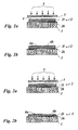
- FIG. 1a shows a carrier substrate 1, which in the exemplary embodiment shown is a banknote on which a multilayer body 2 is applied, which is formed from an adhesive layer 2k and a laminating layer 2l and, for example, as part of the transfer layer of a hot stamping foil Carrier substrate 1 is applied.
- the multilayer body 2 is designed as a transparent multilayer body, so that the multilayer body 2 releases the view of the carrier substrate 1 arranged below it.
- On the carrier substrate 1 facing away from the top of the lamination 21 is transferred by means of a gravure plate 3, an optical paint 4, which is introduced into depressions of the intaglio printing plate 3 is.
- the intaglio printing plate 3 is moved in the direction of the arrows 5 with a high contact pressure against a backing plate located behind the backing substrate and brought into contact with the lamination 2l, wherein the introduced into the wells of the intaglio printing plate 3 optical lacquer dissolves 4 of the wells and on the Top of the lamination 2l adheres. It forms in this way micro-optical structures 6a and 6b (FIG. 1b).
- the optical varnish 4 has a refractive index of about 1.5, because the micro-optical structures 6a and 6b formed by the varnish adjoin air.
- the micro-optical structure 6a is a microlens array
- the micro-optical structure 6b is an asymmetrical relief structure, for example a blazed grating.
- the microlens array may be provided to optically magnify a pictorial representation or alphanumeric characters printed on the carrier substrate.
- the blaze grating may be provided to form an interesting optical effect.
- the boundary contours of the Blaze grid can be designed, for example, as a logo or as an alphanumeric character.
- the intaglio printing plate 3 may be a plate-shaped body or a cylindrical body or a curved plate arranged on a printing cylinder. It can be provided that on a printing cylinder or the like more gravure plates are arranged, for example, register in the register with the micro-optical structures 6a and 6b color layers on the lamination 2, which may form, for example, a background pattern that partially or completely through the micro-optical structures 6a and 6b is covered.
- FIGS. 2a and 2b now show a second embodiment of the method according to the invention.
- FIG. 2 a shows the multilayer body 2 from FIG. 1 a, which is applied to the carrier substrate 1.
- the multilayer body 2 has the adhesive layer 2k and the laminating layer 2l.
- the intaglio printing plate 3 is now used only as an embossing tool with which the micro-optical structures 6a and 6b are molded into the laminating layer 2l under application pressure 5 (see FIG. 2b).
- the micro-optical Structures 6a and 6b may simultaneously constitute a tactile detectable security feature.
- FIGS. 3a to 3c now show a third embodiment of the method according to the invention.
- FIG. 3 a shows a multilayer body 32 that is applied to the carrier substrate 1.
- the multi-layer body 32 like the multi-layer body 2, has the adhesive layer 2k and the lamination layer 2l, on whose side facing away from the adhesive layer an optical lacquer layer 34 is applied.
- the optical structures 6a and 6b are molded by means of the intaglio printing plate 3 under contact pressure 5.
- the multilayer body 32 now has a protective layer 7 applied to the surface of the lacquer layer 34.
- the protective layer 7 is formed with a low refractive index, for example with a refractive index ⁇ 1.5, preferably with a refractive index ⁇ 1.
- the protective layer 7 is a normal resist having a refractive index of about 1.5 and applied by screen printing.
- the optical lacquer layer 34 advantageously has a high refractive index, for example> 1.9. It may be doped to form the high refractive index, for example with nanoparticles.
- the protective layer 7 increases the long-term stability of the molded in the lacquer layer 34 micro-optical structures 6a and 6b and protects them from contamination and / or wear.
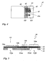
- a banknote 41 carries on its front side a film strip 42 having an OVD 42o and a latent image 42l.
- the latent image 42l is formed in this embodiment of interleaved Blazegittern, resulting in a tilted image.
- Another latent image 41l is executed as a color printed image and printed on the not covered by the film strip 42 surface of the banknote 41.
- the latent images 41l and 42l are in that shown in FIG. 4 illustrated embodiment arranged in alignment with each other in a spaced-apart.
- the latent image 42l shows the letter "O" and the latent image 41l shows the letter "K".
- the latent images are visible only at a predetermined viewing angle. They are invisible from all other points of view, ie latent.
- another OVD 43 is applied to the surface of the banknote 41 not covered by the film strip 42.
- the banknote 41 further has a microlens array 44, which is arranged above an image area 45 in the register.
- the OVDs 42o and 43 are also arranged in register with the microlens array 44 and are partially covered by the microlens array 44.
- any other security document can also be provided.
- the banknote 41 may optionally have a window 46, which projects at least partially into the region of the microlens array.
- a window bank note 50 shown in a schematic sectional view has a carrier substrate 51 which is formed with window-like openings 51fa and 51fb.
- the carrier substrate 51 may be, for example, a paper suitable for banknotes or a plastic film.
- a laminating layer 52 includes optically variable elements (OVD) 52oa and 52ob, which may be, for example, a KINEGRAM®.
- the KINEGRAM® can be fully metallised, demetallised or with a through the aspect ratio of the Surface reliefs may be carried out certain metallization, run with HRI layer or as a multilayer, or designed as a system with color change effects, and there may be a (crosslinked) liquid crystal layer integrated into the system.
- the OVD 52ob is arranged in the window opening 51fb and can therefore be viewed both in reflected light and in transmitted light.
- the OVD 52oa is disposed outside the window openings 51fa and 51fb, and therefore, can only be viewed in reflected light from the front of the sill 50.
- the laminating layer 52 may be formed as a transparent film or as a semitransparent film, for example as a colored film.
- the laminating layer 52 has on its underside an adhesive layer 53, by means of which it is connected to the carrier substrate 51.
- the adhesive layer may be a hot melt adhesive.
- the top of the laminating layer 52 is now printed with different security elements. It is a computer-generated hologram 54g provided with hidden information; a hologram 54h which can effectively represent, for example, alphanumeric characters such as a value impression; tactile features 54t, which may provide, for example, tactile information about the value of the bill; and a microlens array 54m, which in this embodiment is registered in register with the OVD 52ob disposed in the window aperture 51fb.
- the microlens array 54m when viewed from the front of the window banknote 50, produces an optically magnified image of the optical information stored in the OVD 52ob.
- the microlens array 54m when viewing the back side of the sill 50, the microlens array 54m is not optically effective, so that the optical information stored in the OVD 52ob appears to be all natural.
- the holograms 54g and 54h, the tactile feature 54t and the microlens array 54m are applied in intaglio pressure in one operation and therefore arranged in a strict register relative to one another.
- the microlens array 54m is deposited in register with the OVD 52ob, then the other printed elements are also in register with the OVD 52ob and any other elements incorporated in the register in the lamination layer, such as the OVD 52oa.
- the computer generated hologram 54g has pixel areas of different depths.
- the maximum pixel depth in the exemplary embodiment illustrated in FIG. 5 is 1 ⁇ m, the pixels have a size of 1 ⁇ m ⁇ 1 ⁇ m.
- the hidden information is encoded in the pixel depth, which causes a change in the phase angle of the incident light. For example, 8 to 256 different depths may be provided, i. Depending on the number of different depths in a pixel, information from 8 bits to 256 bits can be stored.
Landscapes
- Engineering & Computer Science (AREA)
- Manufacturing & Machinery (AREA)
- Credit Cards Or The Like (AREA)
- Printing Methods (AREA)
- Laminated Bodies (AREA)
Abstract
Description
Die Erfindung betrifft ein Verfahren zur Herstellung eines Mehrschichtkörpers mit mikrooptischen Strukturen, einen mit dem Verfahren hergestellten Mehrschichtkörper sowie ein Sicherheitsdokument mit dem besagten Mehrschichtkörper.The invention relates to a method for producing a multilayer body having microoptical structures, to a multilayer body produced by the method, and to a security document having said multilayer body.
Zur Erhöhung der Fälschungssicherheit von Sicherheitsdokumenten, beispielsweise Banknoten oder Visa, sind zahlreiche Verfahren bekannt.To increase the security against forgery of security documents, such as banknotes or visas, numerous methods are known.
In der
In der
Der Erfindung liegt nun die Aufgabe zugrunde, ein einfaches und kostengünstiges Verfahren zur Herstellung eines Mehrschichtkörpers mit mikrooptischen Strukturen, die im Register zu weiteren Sicherheitsmerkmalen, wie OVDs und bildlichen Darstellungen sind, sowie einen solchen Mehrschichtkörper anzugeben.The invention is based on the object, a simple and inexpensive method for producing a multilayer body with micro-optical structures, to be listed in the register for other security features, such as OVDs and pictorial representations, as well as such a multilayer body.
Die Aufgabe der Erfindung wird durch ein Verfahren zur Herstellung eines Mehrschichtkörpers mit einer aus mikrooptischen Strukturen gebildeten ersten Schicht, die mindestens teilweise eine oder mehrere weitere Schichten überdeckt, die Bildbereiche und/oder Effektbereiche, die einen optischen Effekt ausbilden, aufweisen, gelöst, wobei vorgesehen ist, daß die mikrooptischen Strukturen mittels Intagliodruck auf die unter der ersten Schicht liegende Schicht aufgebracht werden oder in die erste Schicht eingebracht werden. Die Aufgabe wird weiter gelöst durch einen Mehrschichtkörper mit einer aus mikrooptischen Strukturen gebildeten ersten Schicht, die mindestens teilweise eine oder mehrere weitere Schichten überdeckt, die Bildbereiche und/oder Effektbereiche, die einen optischen Effekt ausbilden, aufweisen, wobei vorgesehen ist, daß die mikrooptischen Strukturen mittels Intagliodruck auf die unter der ersten Schicht liegende Schicht aufgebracht sind oder in die erste Schicht eingebracht sind. Die Aufgabe wird weiter gelöst durch ein Sicherheitsdokument mit dem erfindungsgemäßen Mehrschichtkörper.The object of the invention is achieved by a method for producing a multilayer body having a first layer formed from microoptical structures, which at least partially covers one or more further layers, the image areas and / or effect areas, which form an optical effect in that the micro-optical structures are applied by intaglio printing to the layer lying below the first layer or introduced into the first layer. The object is further achieved by a multilayer body having a first layer formed from micro-optical structures, which at least partially covers one or more further layers, the image areas and / or effect areas, which form an optical effect, wherein it is provided that the micro-optical structures are applied by intaglio printing on the underlying layer of the first layer or incorporated in the first layer. The object is further achieved by a security document with the multilayer body according to the invention.
Die Erfindung sieht vor, mikrooptische Strukturen, wie beispielsweise Mikrolinsenarrays oder Blazegitter, mittels Intagliodruck aufzubringen. Bei dem Mehrschichtkörper kann es sich sowohl um eine Transferfolie, die auf ein Sicherheitsdokument aufgebracht wird oder um das Sicherheitsdokument selbst oder um ein Sicherheitsdokument mit Transferfolie handeln.The invention provides to apply micro-optical structures, such as microlens arrays or Blazegitter, by intaglio printing. The multilayer body may be both a transfer film applied to a security document or the security document itself or a security document with transfer film.
Weil mit diesem Verfahren zugleich mehrere mikrooptische Strukturen aufgebracht werden können, reduziert sich der Aufwand zur registergenauen Ausrichtung der mikrooptischen Strukturen beträchtlich, weil es nur darauf ankommt, die eine oder mehreren Druckplatten vor dem Druckprozeß zueinander auszurichten. Danach kann der Mehrschichtkörper in hohen Stückzahlen vervielfältigt werden.Because several micro-optical structures can be applied at the same time with this method, the effort for register-accurate alignment of the micro-optical structures is considerably reduced because it is only important to align the one or more printing plates to one another before the printing process. Thereafter, the multi-layer body can be duplicated in large quantities.
Weiter ist es auch möglich, daß die mikrooptische Struktur in einem endlosen, sich wiederholenden Muster auf den Mehrschichtkörper aufgebracht oder in den Mehrschichtkörper eingebracht wird, ohne im Register zu weiteren mikrooptischen Strukturen zu stehen.Further, it is also possible that the micro-optical structure applied in an endless, repetitive pattern on the multilayer body or in the Multi-layer body is introduced without standing in the register to other micro-optical structures.
Der erfindungsgemäße Mehrschichtkörper zeichnet sich dadurch aus, daß mikrooptische Strukturen erzeugt werden können, die nicht in eine Folienschicht abgeformt sind. Damit werden alle Probleme vermieden, die dadurch entstehen können, wenn mikrooptische Strukturen in einem Rolle-zu-Rolle-Prozeß in eine Transferfolie übertragen werden und anschließend im Register zu anderen Merkmalen auf ein Sicherheitsdokument übertragen werden müssen. Ein weiterer Vorteil ist, daß eine mikrooptische Struktur, die aus untereinander nicht verbundenen optischen Elementen gebildet ist, nicht entfernt und übertragen werden kann, ohne die Struktur zu zerstören. Die Anordnung der mikrooptischen Strukturen im Register erhöht die Fälschungssicherheit des erfindungsgemäßen Mehrschichtkörpers weiter. Der Mehrschichtkörper kann ein besonders strenges Register aufweisen, weil der Aufwand zur Justierung der einzelnen aufeinander abgestimmten Objekte nur einmal entsteht.The multilayer body according to the invention is characterized in that micro-optical structures can be produced which are not molded into a film layer. This avoids all the problems that can arise when microoptical structures are transferred in a roll-to-roll process into a transfer film and subsequently transferred to other security features in the register for other features. Another advantage is that a micro-optic structure formed of interconnected optical elements can not be removed and transferred without destroying the structure. The arrangement of the micro-optical structures in the register further increases the security against forgery of the multilayer body according to the invention. The multi-layer body may have a particularly strict register, because the effort to adjust the individual matched objects arises only once.
Weitere vorteilhafte Ausgestaltungen sind in den Unteransprüchen bezeichnet.Further advantageous embodiments are designated in the subclaims.
Es kann vorgesehen sein, daß die mikrooptischen Strukturen sowie die Bildbereiche und/oder Effektbereiche mittels Tiefdruck aufgebracht werden.It can be provided that the micro-optical structures and the image areas and / or effect areas are applied by gravure printing.
Weiter kann vorgesehen sein, daß sowohl die mikrooptischen Strukturen als auch die Bildbereiche und/oder Effektbereiche im Register aufgebracht werden. Bei den Bildbereichen kann es sich beispielsweise um einfarbige oder mehrfarbige Abbildungen handeln, wie alphanumerische Zeichen, Logos oder dergleichen. Bei den Effektbereichen kann es sich beispielsweise um OVDs handeln, wie ein Hologramm, KINEGRAM®, Blazegitter oder dergleichen.
Bei den Effektbereichen kann es sich auch um taktil erfaßbare Effektbereiche handeln, die beispielsweise in geeigneter Form den Wertaufdruck einer Banknote erfühlbar machen. Taktil erfaßbare Bereiche können weiter einen Schutz gegen Abrieb und/oder Verschmutzung für andere Bereiche bilden.It can further be provided that both the micro-optical structures and the image areas and / or effect areas are applied in the register. The image areas may, for example, be monochrome or multicolor images, such as alphanumeric characters, logos or the like. The effect areas may, for example, be OVDs, such as a hologram, KINEGRAM®, blaze grid or the like.
The effect areas can also be tactile detectable effect areas, which, for example, make the value imprint of a bank note tangible in a suitable form. Tactile detectable areas may further provide protection against abrasion and / or contamination to other areas.
Weil die mikrooptischen Strukturen und/oder die Bildbereiche und/oder die Effektbereiche durch einen Druckprozeß im Register aufgebracht werden, ist kein zusätzlicher Aufwand für das Einrichten bzw. das Justieren der dazu benutzten Fertigungseinrichtung erforderlich. Vielmehr muß nur die Intaglio-Druckplatte registergenau gefertigt werden bzw. mehrere Intaglio-Druckplatten müssen zueinander justiert werden.Because the micro-optical structures and / or image areas and / or the Effect areas are applied by a printing process in the register, no additional effort for setting up or adjusting the purpose used manufacturing equipment is required. Rather, only the Intaglio printing plate must be made accurate register or more Intaglio printing plates must be adjusted to each other.
Es ist auch möglich, in unterschiedlichen Bereichen der Intaglio-Druckplatte unterschiedliche Druckfarben vorzusehen. Es kann beispielsweise vorgesehen sein, daß zwei farbige Flächen an eine mikrooptische Struktur grenzen und alle drei Elemente von einem schwarz ausgelegten Ring umgeben sind, wobei während des Drucks unterschiedlich farbige Tinten und ein optischer Lack gleichzeitig auf das zu bedruckende Substrat übertragen werden. Dadurch ist es möglich, auf einfache Weise die durch die optischen Eigenschaften des Lacks bestimmten optischen Effekte (z.B. farbiger Aufdruck, insbesondere mittels Effektpigmenten) registerhaltig zu den mikrooptischen Strukturen vorzusehen.It is also possible to provide different printing inks in different areas of the Intaglio printing plate. It can be provided, for example, that two colored surfaces border on a micro-optical structure and all three elements are surrounded by a black-lined ring, wherein during printing differently colored inks and an optical paint are simultaneously transferred to the substrate to be printed. This makes it possible to easily provide the optical effects (for example colored imprints, in particular by means of effect pigments) determined by the optical properties of the lacquer in register with the microoptical structures.
Die mit dem erfindungsgemäßen Verfahren erzielte Registergenauigkeit kann nachträglich nur mit sehr hohem Aufwand erreicht werden, so daß das vorgeschlagene Verfahren eine sehr hohe Fälschungssicherheit aufweist. Es ist auch nicht möglich, einzelne Komponenten zu beschaffen und sie miteinander zu vereinen, weil einzelne Komponenten, beispielsweise als Transferfolien oder dergleichen, körperlich nicht existieren. Weitere Vorteile ergeben sich dadurch, daß die mikrooptischen Strukturen und/oder die Bildbereiche und/oder die Effektbereiche einander mindestens teilweise überlappen können, wodurch die Fälschungssicherheit weiter erhöht ist.The register accuracy achieved with the method according to the invention can be achieved later only with great effort, so that the proposed method has a very high security against counterfeiting. It is also not possible to procure individual components and to unify them, because individual components, such as transfer films or the like, do not physically exist. Further advantages result from the fact that the microoptical structures and / or the image areas and / or the effect areas can at least partially overlap one another, as a result of which the security against counterfeiting is further increased.
Es kann vorgesehen sein, daß zur Ausbildung der mikrooptischen Strukturen ein optischer Lack mittels Intagliodruck auf die weiteren Schichten übertragen wird.It can be provided that for the formation of the micro-optical structures, an optical paint is transferred by intaglio printing on the other layers.
Alternativ kann vorgesehen sein, daß auf die weiteren Schichten eine aus dem optischen Lack gebildete Schicht aufgetragen wird und sodann in die aus dem optischen Lack gebildete Schicht mittels Aufpressen einer mindestens bereichsweise farbfreien Intaglio-Druckplatte die mikrooptischen Strukturen abgeformt werden. Es kann also vorgesehen sein, die Tiefdruckplatte mindestens bereichsweise als Prägestempel zu verwenden und die Tiefdruckplatte unter hohem Druck auf die aus dem optischen Lack gebildete Schicht zu pressen, so daß der optische Lack die in der Oberfläche der Tiefdruckplatte angebrachten Vertiefungen vollständig ausfüllt und damit das Oberflächenprofil der Tiefdruckplatte in die Lackschicht abgeformt wird. Es ist also bei dieser Ausführungsvariante vorgesehen, ohne Druckfarbe zu drucken. Im übrigen steht für das erfindungsgemäße Verfahren eine Vielzahl von Lacken zur Verfügung, beispielsweise auch farbige optische Lacke sowie zur Ausbildung der Bildbereiche und/oder der Effektbereiche die gesamte Palette der Tiefdruckfarben.Alternatively, it can be provided that a layer formed from the optical lacquer is applied to the further layers and then the microoptical structures are molded into the layer formed from the optical lacquer by pressing on an intaglio printing plate which is at least partially color-free. It can therefore be provided, the gravure plate at least partially as To use stamp and to press the gravure plate under high pressure on the layer formed from the optical paint, so that the optical paint completely filled in the surface of the gravure plate wells and thus the surface profile of the intaglio plate is molded into the lacquer layer. It is therefore provided in this embodiment, without printing ink. Moreover, a large number of paints are available for the process according to the invention, for example also colored optical paints and for forming the image areas and / or the effect areas the entire range of gravure printing inks.
In einer vorteilhaften Ausgestaltung ist vorgesehen, daß die aus dem optischen Lack gebildete Schicht mittels einer Transferfolie auf die weiteren Schichten übertragen wird. Bei dem optischen Lack kann es sich beispielsweise um einen Photopolymerlack handeln, dessen Viskosität durch Bestrahlung mit UV-Licht einstellbar ist. Allerdings muß der Photopolymerlack nach dem Auftrag mittels UV-Licht ausgehärtet werden.In an advantageous embodiment, it is provided that the layer formed from the optical lacquer is transferred to the further layers by means of a transfer film. The optical lacquer can be, for example, a photopolymer lacquer whose viscosity can be adjusted by irradiation with UV light. However, the photopolymer coating must be cured after application by means of UV light.
In einer vorteilhaften Ausgestaltung ist vorgesehen, daß die Intaglio-Druckplatte mindestens in den farbfreien Bereichen erwärmt wird.In an advantageous embodiment, it is provided that the Intaglio printing plate is heated at least in the color-free areas.
Es kann vorgesehen sein, daß die Intaglio-Druckplatte auf 90 °C bis 100 °C erwärmt wird.It may be provided that the Intaglio printing plate is heated to 90 ° C to 100 ° C.
Weitere Ausführungen sind auf die Ausbildung des erfindungsgemäßen Mehrschichtkörpers gerichtet. Die mikrooptischen Strukturen des Mehrschichtkörpers sind, wie weiter oben bereits ausgeführt, aus hemisphärischen oder pyramidenförmigen oder prismatischen oder zylindrischen optischen Elementen mit ebener Grundfläche gebildet, die durch Intagliodruck auf den Mehrschichtkörper übertragen sind. Dabei können die besagten optischen Elemente beispielsweise aus einem optischen Lack oder dergleichen gebildet sein, oder aus einer Druckfarbe oder aus einem sonstigen druckbaren Material. Die optischen Elemente können aber auch durch Prägung mittels der Druckplatte gebildet sein, also ohne Materialübertragung aus den Vertiefungen der Tiefdruckplatte auf die Oberfläche des Mehrschichtkörpers.Further embodiments are directed to the formation of the multilayer body according to the invention. The micro-optical structures of the multilayer body are, as stated above, formed of hemispherical or pyramidal or prismatic or cylindrical optical elements with a flat base, which are transferred by intaglio pressure on the multilayer body. The said optical elements may be formed, for example, from an optical paint or the like, or from an ink or from any other printable material. However, the optical elements can also be formed by embossing by means of the pressure plate, that is to say without material transfer from the depressions of the gravure printing plate to the surface of the multilayer body.
Es kann vorgesehen sein, daß die mikrooptischen Strukturen einen Periodenabstand von 100 µm bis 0,3 µm aufweisen, vorzugsweise einen Periodenabstand von 20 µm bis 2 µm aufweisen.It can be provided that the micro-optical structures have a period spacing of 100 microns to 0.3 microns, preferably have a period spacing of 20 microns to 2 microns.
Vorteilhafterweise können die mikrooptischen Strukturen eine Tiefe von 50 µm bis 1 µm aufweisen. Es kann also vorgesehen sein, daß die optischen Elemente, aus denen die mikrooptischen Strukturen gebildet sind, eine Höhe von 50 µm bis 1 µm aufweisen.Advantageously, the micro-optical structures can have a depth of 50 μm to 1 μm. It can therefore be provided that the optical elements of which the micro-optical structures are formed, have a height of 50 microns to 1 micron.
Mit den vorgenannten Bereichen des Periodenabstands und der Tiefe der mikrooptischen Strukturen können Tiefen-zu-Breiten-Verhältnisse bzw. Aspektraten in einem breiten Bereich ausgebildet werden. Allerdings können sehr hohe Aspektraten zu mechanisch instabilen Strukturen führen. Solche hohen Aspektraten sind allerdings zur Ausbildung der derzeit bekannten mikrooptischen Strukturen nicht erforderlich.With the above ranges of the period spacing and the depth of the micro-optical structures, depth-to-width ratios and aspect ratios, respectively, can be formed in a wide range. However, very high aspect ratios can lead to mechanically unstable structures. However, such high aspect ratios are not required to form the currently known micro-optical structures.
Weiter kann vorgesehen sein, daß die mikrooptische Struktur eine verborgene Information enthält. Die verborgene Information kann im Auflicht und/oder im Durchlicht auslesbar sein, wie weiter unten ausführlich erläutert.It can further be provided that the micro-optical structure contains hidden information. The hidden information may be readable in reflected light and / or transmitted light, as explained in detail below.
Es kann vorgesehen sein, daß die mikrooptische Struktur als computergeneriertes Hologramm ausgebildet ist. Es kann sich bei der mikrooptischen Struktur auch um ein Gitter, insbesondere ein Blazegitter, und/oder ein Mikrolinsenarray und/oder ein Hologramm und/oder ein KINEGRAM® oder dergleichen handeln. Wenngleich periodische Strukturen im Bereich einer Periodenlänge von 5 µm bis 0,3 µm bevorzugt sind, kann es sich jedoch auch um periodische Strukturen mit einer Periodenlänge > 5 µm, um Mottenaugenstrukturen, insbesondere in Form von sinusförmigen Kreuzgittern mit hohem Aspektverhältnis und/oder um stochastische Strukturen handeln.It can be provided that the micro-optical structure is designed as a computer-generated hologram. It may be at the micro-optical structure may also be a grating, in particular a blazed grating, and / or a micro lens array and / or a hologram and / or a KINEGRAM ® or the like. Although periodic structures in the range of a period length of 5 .mu.m to 0.3 .mu.m are preferred, it is also possible to use periodic structures with a period length of> 5 .mu.m, moth-eye structures, in particular in the form of sinusoidal high aspect ratio cross gratings and / or stochastic Structures act.
Es kann vorgesehen sein, daß die mikrooptische Struktur Pixel mit unterschiedlicher Tiefe aufweist, wobei die Tiefe der Pixel die verborgene Information codiert.It may be provided that the micro-optical structure has pixels of different depth, the depth of the pixels encoding the hidden information.
Weiter kann vorgesehen sein, daß die verborgene Information im Auflicht und/oder im Durchlicht auslesbar ist. Zum Beispiel ist das Auslesen der verborgenen Information mittels eines Lasers möglich, indem der Laserstrahl auf die mikrooptische Struktur gerichtet wird und das von der mikrooptischen Struktur reflektierte oder transmittierte Licht mittels eines Sensors erfaßt und ausgewertet wird. Weiter ist es möglich, daß das von der mikrooptischen Struktur reflektierte oder transmittierte Laserlicht auf einen Schirm projiziert wird und von einem Betrachter ausgewertet wird.It can further be provided that the hidden information in the reflected light and / or transmitted light can be read out. For example, the reading of the hidden information by means of a laser is possible by the laser beam is directed to the micro-optical structure and the light reflected from the micro-optical structure or transmitted light is detected and evaluated by means of a sensor. Further, it is possible that the laser light reflected or transmitted by the micro-optical structure is projected on a screen and evaluated by a viewer.
Die mikrooptische Struktur kann pixelförmige Teilbereiche mit unterschiedlicher Tiefe aufweisen, wobei die Tiefe der pixelförmigen Teilbereiche die verborgene Information codiert.The micro-optical structure may have pixel-shaped partial regions with different depth, the depth of the pixel-shaped partial regions encoding the hidden information.
Es kann vorgesehen sein, daß die mikrooptische Struktur als eine computergenerierte holographische Struktur mit einer Vielzahl optischer Elemente mit unterschiedlicher Höhe ausgebildet ist.It can be provided that the micro-optical structure is formed as a computer-generated holographic structure having a plurality of optical elements with different heights.
Weiter kann vorgesehen sein, daß die Pixeltiefe < 1,5 µm ist.It can further be provided that the pixel depth is <1.5 μm.
Vorzugsweise können 8 bis 256 unterschiedliche Pixeltiefen vorgesehen sein.Preferably, 8 to 256 different pixel depths may be provided.
In einer vorteilhaften Ausbildung ist vorgesehen, daß die Pixel eine Querschnittsfläche von etwa 1 µm x 1 µm aufweisen. Es kann vorgesehen sein, daß die Pixel Seitenlängen von 0,4 µm bis 4 µm aufweisen.In an advantageous embodiment, it is provided that the pixels have a cross-sectional area of approximately 1 μm × 1 μm. It can be provided that the pixels have side lengths of 0.4 μm to 4 μm.
Wenn die vorstehend beschriebene mikrooptische Struktur über einem Fenster eines Trägersubstrats oder in einem transparenten Bereich eines Trägersubstrats angeordnet ist, kann die verborgene Information beispielsweise mit Laserlicht im Durchlicht ausgelesen werden. Dabei tritt der Laserstrahl durch die mikrooptische Struktur hindurch und ein Bild der mikrooptischen Struktur kann auf einem Schirm aufgefangen werden. Bei dem Bild kann es sich um einen Text handeln, wie beispielsweise "OK", oder um ein Bild oder dergleichen, wie beispielsweise die Zeichnung eines Adlers. Als Laserlichtquelle kann beispielsweise ein Laserpointer verwendet werden.If the above-described micro-optical structure is arranged above a window of a carrier substrate or in a transparent area of a carrier substrate, the hidden information can be read out by transmitted light, for example with laser light. The laser beam passes through the micro-optical structure and an image of the micro-optical structure can be collected on a screen. The image may be text, such as "OK," or an image or the like, such as an eagle's drawing. As a laser light source, for example, a laser pointer can be used.
Die Tiefe der oben genannten Pixel, aus denen die mikrooptische Struktur gebildet ist, kann durch folgende Beziehung bestimmt werden: 
Dabei bezeichnet N die Anzahl der unterschiedlichen Pixeltiefen, die für eine sogenannte Kinoform typischerweise N = 64 ist. Wenn ein roter Laserpointer mit einer Wellenlänge λ=635 nm verwendet wird, errechnet sich die maximale Tiefe d, die für einen Phasenverschiebungswinkel Φ=2π und eine Lackschicht mit dem Brechungsindex n1=1,5 benötigt wird, wie folgt: 
Wird dagegen die bezeichnete mikrooptische Struktur auf ein nicht transparentes Substrat, wie Papier aufgebracht, dann wird der Laserstrahl von der Oberfläche der mikrooptischen Struktur reflektiert und das Bild kann beispielsweise auf einem vor der mikrooptischen Struktur angeordneten transparenten Schirm, beispielsweise auf einem Mattglasschirm, aufgefangen werden. Die Bemessungsgleichung lautet nun: 
Wenn ein roter Laserpointer mit einer Wellenlänge λ=635 nm verwendet wird, errechnet sich die maximale Tiefe d, die für einen Phasenverschiebungswinkel Φ=2π in Luft mit der Brechzahl n0=1 benötigt wird, wie folgt: 
Dabei ist das Bild von der "Luftseite" des Oberflächenreliefs her zu betrachten. Bei dem Bild kann es sich wieder um einen Text handeln, wie beispielsweise "OK", oder um ein Bild oder dergleichen, wie beispielsweise die Zeichnung eines Adlers.The picture of the "air side" of the surface relief should be considered. The image may again be a text, such as "OK," or an image or the like, such as the drawing of an eagle.
Zwecks Verbesserung der Sichtbarkeit des in Reflexion projizierten verborgenen Bildes sollte für die mikrooptische Struktur ein Material mit hohem Brechungsindex oder ein gleichmäßig reflektierendes Material verwendet werden.In order to improve the visibility of the hidden image projected in reflection, a high refractive index material or a uniformly reflective material should be used for the microoptical structure.
Es kann vorgesehen sein, daß die optischen Elemente der mikrooptischen Strukturen aus einem optischen Lack gebildet sind.It can be provided that the optical elements of the micro-optical structures are formed from an optical lacquer.
In einer vorteilhaften Ausführung kann vorgesehen sein, daß es sich bei dem optischen Lack um einen hochbrechenden optischen Lack handelt. Ein hoher Brechungsindex kann, wie bereits ausgeführt, das Reflexionsvermögen des Lacks ver-bessern.In an advantageous embodiment it can be provided that the optical lacquer is a high refractive optical lacquer. As already mentioned, a high refractive index can improve the reflectivity of the paint.
Weiter kann vorgesehen sein, daß der optische Lack einen Brechungsindex > 1,9 aufweist.It can further be provided that the optical lacquer has a refractive index> 1.9.
Um einen hohen Brechungsindex zu erhalten, kann als optischer Lack ein Photopolymer verwendet werden, das in dem besagten Tiefdruckprozeß aufgebracht wird.In order to obtain a high refractive index, a photopolymer applied in the said gravure printing process may be used as the optical paint.
In einer vorteilhaften Ausgestaltung ist vorgesehen, daß der optische Lack mit Nanopartikeln dotiert ist. Es kann auch vorgesehen sein, daß der optische Lack mit Farbflocken dotiert ist. Dadurch ist aus dem optischen Lack ein reflektierendes Material erhalten. Die Nanopartikel beinhalten Metalle in Kristallform oder Metallsalze in kolloidaler Form, beispielsweise CdS. Zum Beispiel kann das Einfügen von PbS in eine Polymermatrix den Wert des Brechungsindex auf 2,5 bis 3,0 anheben. Nano-Verbundwerkstoffe aus Polymeren und Gold-Nanopartikeln wurden bereits ausgeführt mit realen Komponenten mit einem so niedrigen Brechungsindex wie 0,96.In an advantageous embodiment, it is provided that the optical lacquer is doped with nanoparticles. It can also be provided that the optical paint is doped with color flakes. As a result, a reflective material is obtained from the optical paint. The nanoparticles include metals in crystal form or metal salts in colloidal form, for example CdS. For example, incorporation of PbS into a polymer matrix can raise the refractive index value to 2.5 to 3.0. Nanocomposites of polymers and gold nanoparticles have already been designed with real components as low as 0.96.
Ebenso kann die mikrooptische Struktur ein OVD, wie ein Hologramm, das die Buchstaben "AB" zeigt, sein und durch Tiefdruck auf die Oberfläche des Mehrschichtkörpers aufgebracht oder eingeprägt sein. Das Oberflächenrelief der Tiefdruckplatte kann beispielsweise erzeugt sein durch 2D- bzw. 3D-Holographie oder durch Verwendung einer Punkt-Matrix-Maschine. Wenn es sich bei dem Oberflächenrelief des Mehrschichtkörpers um ein der Luft ausgesetztes Oberflächenrelief aus nichtdotiertem Kunststoff handelt, kann das Reflexionsvermögen des OVD weniger brilliant sein, als wenn wie üblicherweise HRI-Material oder Metall genutzt ist, doch die optischen Effekte sind vorhanden, wenn auch geschwächt. Durch das vorstehend beschriebene Dotieren des Polymers, in welches das Oberflächenrelief abgeformt ist, kann die Brillianz des OVD erhöht werden.Likewise, the micro-optical structure may be an OVD, such as a hologram showing the letters "AB", and may be gravure printed or embossed on the surface of the multi-layer body. The surface relief of the gravure printing plate can be produced, for example, by 2D or 3D holography or by using a dot-matrix machine. If that is the case Surface relief of the multilayer body is an undoped plastic surface relief exposed to air, the reflectivity of the OVD may be less brilliant than when HRI material or metal is used as usual, but the optical effects are present, albeit weakened. By the above-described doping of the polymer into which the surface relief is molded, the brilliance of the OVD can be increased.
Es kann vorgesehen sein, daß die die mikrooptische Strukturen aufweisende erste Schicht des Mehrschichtkörpers mit einer Schutzschicht überzogen ist. Diese Schutzschicht-kann typischerweise mittels Siebdruck aufgebracht sein.It can be provided that the micro-optical structures having first layer of the multilayer body is coated with a protective layer. This protective layer may typically be screen printed.
Es kann weiter vorgesehen sein, daß es sich um eine niedrigbrechende Schutzschicht handelt.It may further be provided that it is a low-refractive protective layer.
In einer vorteilhaften Ausbildung kann vorgesehen sein, daß die Schutzschicht einen Brechungsindex < 1,5 aufweist. Wie bereits weiter oben ausgeführt, kann die Kombination einer niedrigbrechenden Schutzschicht mit einer hochbrechenden mikrooptischen Struktur bzw. einer mikrooptischen Struktur mit HRI-Oberfläche eine besonders gute Reflexion an der mikrooptischen Struktur hervorrufen.In an advantageous embodiment it can be provided that the protective layer has a refractive index <1.5. As already stated above, the combination of a low-refractive-index protective layer with a high-index micro-optical structure or a micro-optical structure with an HRI surface can produce particularly good reflection at the micro-optical structure.
Wie bereits weiter oben beispielhaft ausgeführt, kann ein nichttransparentes Sicherheitsdokument mit einem oder mehreren Fenstern ausgebildet sein. Es kann dann vorgesehen sein, daß der Mehrschichtkörper mindestens teilweise über einem in das Sicherheitsdokument eingebrachten Fenster angeordnet ist. Bei dem Sicherheitsdokument kann es sich beispielsweise um eine Fensterbanknote handeln. Das Sicherheitsdokument kann nun folgende Sicherheitsmerkmale aufweisen, die sämtlich in einem Fertigungsschritt von der Tiefdruckplatte auf das Sicherheitsdokument und/oder den Mehrschichtkörper übertragen sind:
- Sicherheitsmerkmale mit verborgener Information,
- OVDs, wie zum Beispiel Hologramme,
- Mikrolinsenarrays für die Erzeugung von Kippbildern (Nimble Image Effect),
- taktile Elemente,
- Arrays von Zylinderlinsen für die Erzeugung von eindimensionalem Moiré-Effekt oder "scrambled indicia",
- Retroreflektoren,
- Fresnel-Linsen, beispielsweise als Lupe,
- Flip Elemente, beispielsweise Wechsel von einer Währungsangabe zu einer Wertangabe beim Kippen des Sicherheitsdokuments,
- Oberflächenreliefs.
- Security features with hidden information,
- OVDs, such as holograms,
- Microlens arrays for the generation of tilt images (Nimble Image Effect),
- tactile elements,
- Arrays of cylindrical lenses for the creation of one-dimensional moiré effect or "scrambled indicia",
- Retroreflectors
- Fresnel lenses, for example as a magnifying glass,
- Flip elements, such as changing from a currency to a value when tipping the security document,
- Surface relief.
Im folgenden wird die Erfindung anhand von mehreren Ausführungsbeispielen unter Zuhilfenahme der beiliegenden Zeichnungen beispielhaft verdeutlicht.In the following the invention will be clarified by way of example with reference to several embodiments with the aid of the accompanying drawings.
Es zeigen
- Fig. 1a und 1b
- Verfahrensschritte eines ersten Ausführungsbeispiels des erfindungsgenäßen Verfahrens in schematischer Darstellung;
- Fig. 2a und 2b
- Verfahrensschritte eines zweiten Ausführungsbeispiels des erfindungsgemäßen Verfahrens in schematischer Darstellung;
- Fig. 3a bis 3c
- Verfahrensschritte eines dritten Ausführungsbeispiels des erfindungsgemäßen Verfahrens in schematischer Darstellung;
- Fig. 4
- ein erstes Anwendungsbeispiel des erfindungsgemäßen Verfahrens;
- Fig. 5
- ein zweites Anwendungsbeispiel des erfindungsgemäßen Verfahrens.
- Fig. 1a and 1b
- Method steps of a first embodiment of the erfindungsgenäßen method in a schematic representation;
- Fig. 2a and 2b
- Method steps of a second embodiment of the method according to the invention in a schematic representation;
- Fig. 3a to 3c
- Method steps of a third embodiment of the method according to the invention in a schematic representation;
- Fig. 4
- a first example of application of the method according to the invention;
- Fig. 5
- a second example of application of the method according to the invention.
Fig. 1a zeigt ein Trägersubstrat 1, bei dem es sich in dem dargestellten Ausführungsbeispiel um eine Banknote handelt, auf das ein Mehrschichtkörper 2 aufgebracht ist, der aus einer Kleberschicht 2k und einer Laminierschicht 2l gebildet ist und beispielsweise als Teil der Transferlage einer Heißprägefolie auf das Trägersubstrat 1 appliziert ist. Der Mehrschichtkörper 2 ist als transparenter Mehrschichtkörper ausgebildet, so daß der Mehrschichtkörper 2 den Blick auf das unter ihm angeordnete Trägersubstrat 1 freigibt. Auf die dem Trägersubstrat 1 abgewandte Oberseite der Laminierschicht 21 wird mittels einer Tiefdruckplatte 3 ein optischer Lack 4 übertragen, der in Vertiefungen der Tiefdruckplatte 3 eingebracht ist. Die Tiefdruckplatte 3 wird in Richtung der Pfeile 5 mit einer hohen Anpreßkraft gegen eine hinter dem Trägersubstrat liegende Gegendruckplatte bewegt und in Kontakt mit der Laminierschicht 2l gebracht, wobei sich der in die Vertiefungen der Tiefdruckplatte 3 eingebrachte optische Lack 4 aus den Vertiefungen löst und auf der Oberseite der Laminierschicht 2l haftet. Er bildet auf diese Weise mikrooptische Strukturen 6a und 6b (Fig. 1b) aus. Der optische Lack 4 weist eine Brechzahl von etwa 1,5 auf, weil die durch den Lack ausgebildeten mikrooptischen Strukturen 6a und 6b an Luft grenzen.FIG. 1a shows a
Bei der mikrooptischen Struktur 6a handelt es sich um ein Mikrolinsenarray, bei der mikrooptischen Struktur 6b handelt es sich um eine asymmetrische Reliefstruktur, beispielsweise ein Blazegitter. Das Mikrolinsenarray kann vorgesehen sein, um eine auf das Trägersubstrat aufgedruckte bildliche Darstellung oder alphanumerische Zeichen optisch zu vergrößern. Das Blazegitter kann vorgesehen sein, um einen interessanten optischen Effekt auszubilden. Die Begrenzungskonturen des Blazegitters können beispielsweise als Logo oder als alphanumerisches Zeichen ausgebildet sein.The
Bei der Tiefdruckplatte 3 kann es sich um einen plattenförmigen Körper handeln oder um einen zylindrischen Körper oder um eine auf einem Druckzylinder angeordnete gewölbte Platte. Es kann vorgesehen sein, daß auf einem Druckzylinder oder dergleichen weitere Tiefdruckplatten angeordnet sind, die beispielsweise im Register mit den mikrooptischen Strukturen 6a und 6b Farbschichten auf die Laminierschicht 2 auftragen, die beispielsweise ein Hintergrundmuster bilden können, das partiell oder vollständig durch die mikrooptischen Strukturen 6a und 6b überdeckt ist.The
Die Fig. 2a und 2b zeigen nun ein zweites Ausführungsbeispiel des erfindungsgemäßen Verfahrens.FIGS. 2a and 2b now show a second embodiment of the method according to the invention.
Fig. 2a zeigt den Mehrschichtkörper 2 aus Fig. 1a, der auf das Trägersubstrat 1 aufgebracht ist. Der Mehrschichtkörper 2 weist die Kleberschicht 2k und die Laminierschicht 2l auf. Die Tiefdruckplatte 3 wird nunmehr nur als Prägewerkzeug verwendet, mit dem unter Anpreßdruck 5 die mikrooptischen Strukturen 6a und 6b in die Laminierschicht 2l abgeformt werden (siehe Fig. 2b). Die mikrooptischen Strukturen 6a und 6b können gleichzeitig ein taktil erfaßbares Sicherheitsmerkmal bilden.FIG. 2 a shows the multilayer body 2 from FIG. 1 a, which is applied to the
Die Fig. 3a bis 3c zeigen nun ein drittes Ausführungsbeispiel des erfindungsgemäßen Verfahrens.FIGS. 3a to 3c now show a third embodiment of the method according to the invention.
Fig. 3a zeigt einen Mehrschichtkörper 32, der auf das Trägersubstrat 1 aufgebracht ist. Der Mehrschichtkörper 32 weist wie der Mehrschichtkörper 2 die Kleberschicht 2k und die Laminierschicht 2l auf, auf deren der Kleberschicht abgewandten Seite eine optische Lackschicht 34 aufgebracht ist. In die optische Lackschicht 34 werden mittels der Tiefdruckplatte 3 unter Anpreßdruck 5 die optischen Strukturen 6a und 6b (siehe Fig. 3b) abgeformt.FIG. 3 a shows a multilayer body 32 that is applied to the
In Fig. 3c zeigt nun im dritten Verfahrensschritt den Mehrschichtkörper 32 mit einer auf der Oberfläche der Lackschicht 34 aufgebrachten Schutzschicht 7. Die Schutzschicht 7 ist mit einem niedrigen Brechungsindex ausgebildet, beispielsweise mit einem Brechungsindex < 1,5, vorzugsweise mit einem Brechungsindex ≈ 1. In einer bevorzugten Ausführung handelt es sich bei der Schutzschicht 7 um einen normalen Abdecklack, der einen Brechungsindex von ungefähr 1,5 aufweist und im Siebdruckverfahren aufgebracht wird. In diesem Fall weist die optische Lackschicht 34 vorteilhafterweise einen hohen Brechungsindex auf, beispielsweise > 1,9. Sie kann zur Ausbildung des hohen Brechungsindex dotiert sein, beispielsweise mit Nanopartikeln. Die Schutzschicht 7 erhöht die Langzeitstabilität der in der Lackschicht 34 abgeformten mikrooptischen Strukturen 6a und 6b und schützt diese vor Verschmutzung und/oder Abnutzung.In FIG. 3c, in the third method step, the multilayer body 32 now has a
Fig. 4 zeigt nun ein Anwendungsbeispiel des erfindungsgemäßen Verfahrens.4 now shows an example of application of the method according to the invention.
Eine Banknote 41 trägt auf ihrer Vorderseite einen Folienstreifen 42, der ein OVD 42o und ein latentes Bild 42l aufweist. Das latente Bild 42l ist in diesem Ausführungsbeispiel aus ineinander verschachtelten Blazegittern gebildet, die ein Kippbild ergeben. Ein weiteres latentes Bild 41l ist als farbiges gedrucktes Bild ausgeführt und auf die nicht von dem Folienstreifen 42 überdeckte Oberfläche der Banknote 41 aufgedruckt. Die latenten Bilder 41l und 42l sind in dem in Fig. 4 dargestellten Ausführungsbeispiel in einer Flucht voneinander beabstandet angeordnet. Das latente Bild 42l zeigt den Buchstaben "O" und das latente Bild 41l zeigt den Buchstaben "K". Die latenten Bilder sind nur unter einem vorbestimmten Betrachtungswinkel sichtbar. Sie sind aus allen anderen Blickrichtungen unsichtbar, d.h. latent.A
Neben dem OVD 42o ist ein weiteres OVD 43 auf der nicht von dem Folienstreifen 42 überdeckten Oberfläche der Banknote 41 aufgebracht.In addition to the OVD 42o, another
Die Banknote 41 weist weiter ein Mikrolinsenarray 44 auf, das über einem Bildbereich 45 im Register angeordnet ist. Auch die OVD 42o und 43 sind im Register zu dem Mikrolinsenarray 44 angeordnet und sind teilweise von dem Mikrolinsenarray 44 überdeckt.The
Die Anordnung im Register des Mikrolinsenarrays 44, des Bildbereichs 45, sowie der OVDs 42o und 43 ist durch die Anwendung des weiter oben beschriebenen erfindungsgemäßen Verfahrens unter den Bedingungen der Massenfertigung möglich, weil sämtliche bezeichneten Elemente in einem Tiefdruckprozeß auf einer Anlage auf die Banknote 41 aufgebracht sind.The arrangement in the register of the
Anstelle der Banknote kann auch ein beliebiges anderes Sicherheitsdokument vorgesehen sein.Instead of the banknote, any other security document can also be provided.
Die Banknote 41 kann optional ein Fenster 46 aufweisen, das zumindest bereichsweise in den Bereich des Mikrolinsenarrays hineinragt.The
Fig. 5 zeigt nun ein zweites Anwendungsbeispiel des erfindungsgemäßen Verfahrens. Eine in einer schematischen Schnittansicht dargestellte Fensterbanknote 50 weist ein Trägersubstrat 51 auf, das mit fensterartigen Durchbrüchen 51fa und 51fb ausgebildet ist. Bei dem Trägersubstrat 51 kann es sich beispielsweise um ein für Banknoten geeignetes Papier oder um eine Kunststoffolie handeln. Eine Laminierschicht 52 weist optisch variable Elemente (OVD) 52oa und 52ob auf, bei denen es sich beispielsweise um ein KINEGRAM® handeln kann. Das KINEGRAM® kann völlig metallisiert, demetallisiert oder mit einer durch die Aspektrate des Oberflächenreliefs bestimmten Metallisation ausgeführt sein, mit HRI-Schicht oder als Multilayer ausgeführt sein, oder als System mit Farbwechseleffekten ausgebildet sein, und es kann eine (vernetzte) Flüssigkristallschicht in das System integriert sein. Das OVD 52ob ist in dem Fensterdurchbruch 51fb angeordnet und kann deshalb sowohl im Auflicht als auch im Durchlicht betrachtet werden. Das OVD 52oa ist außerhalb der Fensterdurchbrüche 51fa und 51fb angeordnet und kann deshalb nur im Auflicht von der Vorderseite der Fensterbanknote 50 her betrachtet werden. Die Laminierschicht 52 kann als transparente Folie oder als halbtransparente Folie ausgebildet sein, beispielsweise als farbige Folie.5 now shows a second example of application of the method according to the invention. A window bank note 50 shown in a schematic sectional view has a
Die Laminierschicht 52 weist auf ihrer Unterseite eine- Kleberschicht 53 auf, mittels der sie mit dem Trägersubstrat 51 verbunden ist. Bei der Kleberschicht kann es sich um einen Heißkleber handeln.The
Die Oberseite der Laminierschicht 52 ist nun mit unterschiedlichen Sicherheitselementen bedruckt. Es handelt sich dabei um ein computergeneriertes Hologramm 54g, das mit einer versteckten Information versehen ist; um ein Hologramm 54h, das beispielsweise in effektvoller Weise alphanumerische Zeichen, wie einen Werteindruck, wiedergeben kann; um taktile Merkmale 54t, die beispielsweise eine ertastbare Information über den Wert der Banknote bereitstellen können; und um ein Mikrolinsenarray 54m, das in diesem Ausführungsbeispiel im Register zu dem in dem Fensterdurchbruch 51fb angeordneten OVD 52ob aufgebracht ist. Das Mikrolinsenarray 54m erzeugt bei Betrachtung der Vorderseite der Fensterbanknote 50 ein optisch vergrößertes Abbild der in dem OVD 52ob gespeicherten optischen Information. Bei Betrachtung der Rückseite der Fensterbanknote 50 ist dagegen das Mikrolinsenarray 54m optisch nicht wirksam, so daß die in dem OVD 52ob gespeicherte optische Information in natürlicher Größe erscheint. Wie bereits weiter oben beschrieben, sind die Hologramme 54g und 54h, das taktile Merkmal 54t und das Mikrolinsenarray 54m im Intaglio-Druck in einem Arbeitsschritt aufgebracht und deshalb zueinander in einem strengen Register angeordnet. Wenn also das Mikrolinsenarray 54m im Register zu dem OVD 52ob aufgebracht ist, dann sind auch die übrigen aufgedruckten Elemente im Register zu dem OVD 52ob und allen weiteren in der Laminierschicht im Register eingebrachten Elementen, wie dem OVD 52oa.The top of the
Das computergenerierte Hologramm 54g weist Pixelbereiche mit unterschiedlicher Tiefe auf. Die maximale Pixeltiefe beträgt in dem in Fig. 5 dargestellten Ausführungsbeispiel 1 µm, die Pixel haben eine Größe von 1 µm x 1 µm. Die versteckte Information ist in der Pixeltiefe codiert, die eine Änderung der Phasenlage des einfallenden Lichtes hervorruft. Es können beispielsweise 8 bis 256 verschiedene Tiefen vorgesehen sein, d.h. je nach Anzahl der unterschiedlichen Tiefen in einem Pixel Informationen von 8 bit bis 256 bit gespeichert sein.The computer generated
Claims (31)
dadurch gekennzeichnet,
daß die mikrooptischen Strukturen (6a, 6b, 54g, 54h, 54m) mittels Intagliodruck auf die unter der ersten Schicht liegende Schicht aufgebracht werden oder in die erste Schicht eingebracht werden.Method for producing a multilayer body with a first layer formed from microoptical structures, which at least partially covers one or more further layers, which have image areas and / or effect areas which form an optical effect,
characterized,
in that the microoptical structures (6a, 6b, 54g, 54h, 54m) are applied by intaglio printing to the layer below the first layer or introduced into the first layer.
dadurch gekennzeichnet,
daß sowohl die mikrooptischen Strukturen (6a, 6b, 54g, 54h, 54m) als auch die Bildbereiche (45) und/oder Effektbereiche (41l, 42l, 42o, 43, 54t) mittels Intagliodruck aufgebracht werden.Method according to claim 1,
characterized,
in that both the microoptical structures (6a, 6b, 54g, 54h, 54m) and the image areas (45) and / or effect areas (41l, 42l, 42o, 43, 54t) are applied by intaglio printing.
dadurch gekennzeichnet,
daß die mikrooptischen Strukturen (6a, 6b, 54g, 54h, 54m) sowie die Bildbereiche (45) und/oder Effektbereiche (41l, 42l, 42o, 43, 54t) mit der selben Druckplatte und/oder der selben Druckmaschine im Register aufgebracht werden.Method according to claim 2,
characterized,
in that the microoptical structures (6a, 6b, 54g, 54h, 54m) and the image areas (45) and / or effect areas (41l, 42l, 42o, 43, 54t) are applied in register with the same printing plate and / or the same printing machine ,
dadurch gekennzeichnet,
daß zum Aufbringen der mikrooptischen Strukturen (6a, 6b) ein optischer Lack (4) mittels Intagliodruck auf die weiteren Schichten übertragen wird.Method according to one of the preceding claims,
characterized,
in that for applying the micro-optical structures (6a, 6b) an optical lacquer (4) Intaglio pressure is transferred to the other layers.
dadurch gekennzeichnet,
daß auf die weiteren Schichten eine aus dem optischen Lack (4) gebildete Schicht (24) aufgetragen wird und sodann in die aus dem optischen Lack gebildete Schicht (24) mittels Aufpressen einer Intaglio-Druckplatte die mikrooptischen Strukturen (6a, 6b) abgeformt werden.Method according to one of claims 1 to 3,
characterized,
in that a layer (24) formed from the optical lacquer (4) is applied to the further layers and then the microoptical structures (6a, 6b) are molded into the layer (24) formed from the optical lacquer by pressing on an intaglio printing plate.
dadurch gekennzeichnet,
daß die aus dem optischen Lack (4) gebildete Schicht (24) mittels einer Transferfolie auf die weiteren Schichten übertragen wird.Method according to claim 5,
characterized,
that from the optical coating (4) is transferred layer formed (24) by means of a transfer film on the further layers.
dadurch gekennzeichnet,
daß die Intaglio-Druckplatte erwärmt wird, insbesondere daß die Intaglio-Druckplatte auf 90 °C bis 100 °C erwärmt wird.Method according to claim 5 or 6,
characterized,
that the Intaglio printing plate is heated, in particular that the Intaglio printing plate is heated to 90 ° C to 100 ° C.
dadurch gekennzeichnet,
daß auf die Intaglio-Druckplatte in einem ersten Bereich Lack, insbesondere farbiger Lack, und in einem zweiten Bereich kein Lack aufgebracht wird und sodann durch Aufpressen der Intaglio-Druckplatte die mikrooptischen Strukturen im zweiten Bereich abgeformt werden.Method according to claim 5,
characterized,
that no lacquer is applied to the Intaglio printing plate in a first area lacquer, especially colored lacquer, and in a second area and then the micro-optical structures are molded in the second area by pressing the Intaglio pressure plate.
dadurch gekennzeichnet,
daß die mikrooptischen Strukturen (6a, 6b, 54g, 54h, 54m) mittels Intagliodruck auf die unter der ersten Schicht liegende Schicht aufgebracht sind oder in die erste Schicht eingebracht sind.Multilayer body having a first layer formed from micro-optical structures, which at least partially covers one or more further layers, which have image areas and / or effect areas which form an optical effect,
characterized,
in that the microoptical structures (6a, 6b, 54g, 54h, 54m) are applied by intaglio printing to the layer underlying the first layer or into the first layer are introduced.
dadurch gekennzeichnet,
daß die mikrooptischen Strukturen (6a, 6b) aus hemisphärischen oder pyramidenförmigen oder prismatischen oder zylindrischen optischen Elementen mit ebener Grundfläche gebildet sind, wobei die ebenen Grundflächen der besagten optischen Elemente mindestens eine einer weiteren Schicht zugewandte Ebene aufspannen, welche die Grenzfläche zu der oder den weiteren Schicht bzw. Schichten bildet, auf der die optischen Elemente angeordnet sind.Multilayer body according to claim 9,
characterized,
in that the micro-optical structures (6a, 6b) are formed from hemispherical or pyramidal or prismatic or cylindrical planar-plane optical elements, the planar bases of said optical elements defining at least one plane facing another layer, which interface with the one or more Layer or layers forms, on which the optical elements are arranged.
dadurch gekennzeichnet,
daß die mikrooptischen Strukturen (6a, 6b, 54g, 54h, 54m) einen Periodenabstand von 100 µm bis 0,3 µm aufweisen.Multilayer body according to claim 9 or 10,
characterized,
in that the microoptical structures (6a, 6b, 54g, 54h, 54m) have a period spacing of 100 μm to 0.3 μm.
dadurch gekennzeichnet,
daß die mikrooptischen Strukturen (6a, 6b, 54g, 54h, 54m) einen Periodenabstand von 20 µm bis 2 µm aufweisen.Multilayer body according to claim 11,
characterized,
in that the microoptical structures (6a, 6b, 54g, 54h, 54m) have a period spacing of 20 μm to 2 μm.
dadurch gekennzeichnet,
daß die mikrooptischen Strukturen eine Tiefe von 50 µm bis 1 µm aufweisen.Multilayer body according to one of claims 9 to 12,
characterized,
that the micro-optical structures have a depth of 50 microns to 1 micron.
dadurch gekennzeichnet,
daß die mikrooptische Struktur (54g) eine verborgene Information enthält.Multilayer body according to one of claims 9 to 13,
characterized,
that the micro-optical structure (54g) contains hidden information.
dadurch gekennzeichnet,
daß die verborgene Information im Auflicht und/oder im Durchlicht auslesbar ist.Multilayer body according to claim 14,
characterized,
that the hidden information in the reflected light and / or transmitted light is readable.
dadurch gekennzeichnet,
daß die mikrooptische Struktur pixelförmige Teilbereiche mit unterschiedlicher Tiefe aufweist, wobei die Tiefe der pixelförmigen Teilbereiche die verborgene Information codiert.Multilayer body according to claim 14 or 15,
characterized,
in that the micro-optical structure has pixel-shaped partial regions with different depth, the depth of the pixel-shaped partial regions coding the hidden information.
dadurch gekennzeichnet,
daß die mikrooptische Struktur als eine computergenerierte holographische Struktur mit einer Vielzahl optischer Elemente mit unterschiedlicher Höhe ausgebildet ist.Multilayer body according to one of claims 9 to 16,
characterized,
in that the micro-optical structure is designed as a computer-generated holographic structure with a multiplicity of optical elements of different heights.
dadurch gekennzeichnet,
daß die Tiefe der pixelförmigen Teilbereiche < 1,5 µm ist.Multilayer body according to claim 17,
characterized,
that the depth of the pixel-shaped subregions is <1.5 micron.
dadurch gekennzeichnet,
daß 8 bis 256 unterschiedliche Tiefen der pixelförmigen Teilbereiche vorgesehen sind.Multilayer body according to one of claims 16 to 18,
characterized,
that 8 to 256 different depths of the pixel-shaped portions are provided.
dadurch gekennzeichnet,
daß die pixelförmigen Teilbereiche Seitenlängen von 0,4 µm bis 4 µm aufweisen.Multilayer body according to one of claims 16 to 19,
characterized,
in that the pixel-shaped partial regions have side lengths of 0.4 μm to 4 μm.
dadurch gekennzeichnet,
daß die optischen Elemente aus einem optischen Lack (4, 24) gebildet sind.Multilayer body according to one of claims 9 to 20,
characterized,
in that the optical elements are formed from an optical lacquer (4, 24).
daß es sich bei dem optischen Lack (4, 24) um einen hochbrechenden optischen Lack handelt.Multilayer body according to Claim 21,
in that the optical lacquer (4, 24) is a high-index optical lacquer.
dadurch gekennzeichnet,
daß der optische Lack (4, 24) einen Brechungsindex > 1,9 aufweist.Multilayer body according to Claim 22,
characterized,
that the optical coating (4, 24) has a refractive index> 1.9.
dadurch gekennzeichnet,
daß der optische Lack (4, 24) mit Nanopartikeln dotiert ist.Multilayer body according to one of Claims 21 to 23,
characterized,
that the optical coating (4, 24) is doped with nanoparticles.
dadurch gekennzeichnet,
daß es sich bei den Nanopartikeln um Metalle und/oder Metallegierungen und/oder Metallsalze handelt.Multilayer body according to Claim 24,
characterized,
that the nanoparticles are metals and / or metal alloys and / or metal salts.
dadurch gekennzeichnet,
daß es sich bei den Nanopartikeln um Farbpartikel handelt.Multilayer body according to Claim 24,
characterized,
that the nanoparticles are colored particles.
dadurch gekennzeichnet,
daß die die mikrooptischen Strukturen (6a, 6b, 54g, 54h, 54m) aufweisende erste Schicht mit einer Schutzschicht (7) überzogen ist.Multilayer body according to one of claims 9 to 26,
characterized,
in that the first layer comprising the microoptical structures (6a, 6b, 54g, 54h, 54m) is coated with a protective layer (7).
dadurch gekennzeichnet,
daß es sich um eine niedrigbrechende Schutzschicht handelt.Multilayer body according to Claim 27,
characterized,
that it is a low-refractive protection layer.
dadurch gekennzeichnet,
daß die Schutzschicht einen Brechungsindex < 1,5 aufweist.Multilayer body according to Claim 28,
characterized,
that the protective layer has a refractive index <1.5.
dadurch gekennzeichnet,
daß der Mehrschichtkörper mindestens teilweise über einem in das Sicherheitsdokument eingebrachten Fenster angeordnet ist.Security document according to claim 30,
characterized,
that the multilayer body is disposed at least partially over a incorporated in the security document window.
Applications Claiming Priority (1)
| Application Number | Priority Date | Filing Date | Title |
|---|---|---|---|
| DE102006032660A DE102006032660A1 (en) | 2006-07-13 | 2006-07-13 | Multi-layer body with micro-optics |
Publications (4)
| Publication Number | Publication Date |
|---|---|
| EP1878584A2 true EP1878584A2 (en) | 2008-01-16 |
| EP1878584A3 EP1878584A3 (en) | 2008-07-23 |
| EP1878584B1 EP1878584B1 (en) | 2014-04-30 |
| EP1878584B2 EP1878584B2 (en) | 2019-10-23 |
Family
ID=38543781
Family Applications (1)
| Application Number | Title | Priority Date | Filing Date |
|---|---|---|---|
| EP07013569.4A Active EP1878584B2 (en) | 2006-07-13 | 2007-07-11 | Multi-layer body with micro optics |
Country Status (7)
| Country | Link |
|---|---|
| US (1) | US20080024846A1 (en) |
| EP (1) | EP1878584B2 (en) |
| CA (1) | CA2593340C (en) |
| DE (1) | DE102006032660A1 (en) |
| DK (1) | DK1878584T4 (en) |
| ES (1) | ES2486341T5 (en) |
| RU (1) | RU2435675C2 (en) |
Cited By (10)
| Publication number | Priority date | Publication date | Assignee | Title |
|---|---|---|---|---|
| WO2009083146A2 (en) * | 2007-12-21 | 2009-07-09 | Giesecke & Devrient Gmbh | Method for producing a microstructure |
| DE102008036482A1 (en) | 2008-08-05 | 2010-02-11 | Giesecke & Devrient Gmbh | Method for producing microlenses |
| WO2010054671A1 (en) * | 2008-11-12 | 2010-05-20 | Nivatex Limited | Data carrier with microcontours and production method |
| WO2011015384A1 (en) | 2009-08-04 | 2011-02-10 | Giesecke & Devrient Gmbh | Security arrangement |
| WO2011029602A3 (en) * | 2009-09-11 | 2011-05-05 | Ovd Kinegram Ag | Multilayer body |
| FR3030362A1 (en) * | 2014-12-17 | 2016-06-24 | Oberthur Technologies | SECURITY DEVICE |
| EP3124285A1 (en) * | 2015-07-27 | 2017-02-01 | Giesecke & Devrient GmbH | Embossing tool for producing a security element with an optically variable structure |
| WO2018060308A1 (en) * | 2016-09-29 | 2018-04-05 | Fraunhofer-Gesellschaft zur Förderung der angewandten Forschung e.V. | Electric energy storage unit with structured arrestor plate and method for structuring an arrester plate of an electric energy storage unit |
| EP3366474A1 (en) | 2017-02-22 | 2018-08-29 | KBA-NotaSys SA | Printing press with in-line casting device for the replication and formation of a micro-optical structure |
| WO2020177923A1 (en) | 2019-03-06 | 2020-09-10 | Giesecke+Devrient Currency Technology Gmbh | Lens pigment, method for producing same, valuable document and printing ink |
Families Citing this family (15)
| Publication number | Priority date | Publication date | Assignee | Title |
|---|---|---|---|---|
| DE102009007779C5 (en) | 2009-02-04 | 2017-07-27 | Bundesdruckerei Gmbh | A method for producing a visually perceptible without technical aids security feature, security feature for plastic-based value or security document and document with at least one such security feature |
| DE102010019766A1 (en) | 2010-05-07 | 2011-11-10 | Giesecke & Devrient Gmbh | Method for producing a microstructure on a support |
| RU2480550C1 (en) * | 2011-12-23 | 2013-04-27 | Федеральное Государственное Унитарное Предприятие "Гознак" (Фгуп "Гознак") | Polymer multi-layer compound protective element and method of its production |
| DE102012204340A1 (en) * | 2012-03-19 | 2013-09-19 | Bundesdruckerei Gmbh | Security document with a perforation window and method for its production |
| GB201208137D0 (en) * | 2012-05-10 | 2012-06-20 | Rue De Int Ltd | Security devices and methods of manufacture therefor |
| CN103847289B (en) * | 2012-11-29 | 2016-03-23 | 中钞特种防伪科技有限公司 | There is the optical anti-counterfeit element reproducing hidden image and the product made with it |
| DE102013016776A1 (en) * | 2013-10-09 | 2015-04-09 | Giesecke & Devrient Gmbh | Process for producing a lens structure |
| DE102013016775A1 (en) * | 2013-10-09 | 2015-04-09 | Giesecke & Devrient Gmbh | Method of making a portable data carrier |
| DE102014018512A1 (en) | 2014-12-12 | 2016-06-16 | Giesecke & Devrient Gmbh | Optically variable security element |
| US20170123112A1 (en) * | 2015-10-28 | 2017-05-04 | Joel Scott Scarbrough | Multilayered Press Stable Lens Array Film |
| GB2580069B (en) * | 2018-12-20 | 2022-06-15 | De La Rue Int Ltd | Security documents and methods of manufacture thereof |
| DE102019111647A1 (en) * | 2019-05-06 | 2020-11-12 | HELLA GmbH & Co. KGaA | Lighting device for a vehicle and a method for producing a lighting device for a vehicle |
| AU2020279477C1 (en) | 2019-05-20 | 2023-08-17 | Crane & Co., Inc. | Use of nanoparticles to tune index of refraction of layers of a polymeric matrix to optimize microoptic (mo) focus |
| EP3888929B1 (en) | 2020-03-31 | 2022-05-11 | NWM Research Spolka z ograniczona Odpowiedzialnoscia Spolka komandytowa | A method of manufacturing a discretized optical security microstructure on a substrate and a shim for use in the method |
| WO2022053826A1 (en) * | 2020-09-11 | 2022-03-17 | De La Rue International Limited | Security devices and methods of manufacture thereof |
Citations (2)
| Publication number | Priority date | Publication date | Assignee | Title |
|---|---|---|---|---|
| EP0429782A1 (en) | 1989-12-01 | 1991-06-05 | Landis & Gyr Technology Innovation AG | Arrangement for improving the falsification safety of a document of value |
| WO2002091041A1 (en) | 2001-05-08 | 2002-11-14 | Commonwealth Scientific And Industrial Research Organisation | An optical device and methods of manufacture |
Family Cites Families (14)
| Publication number | Priority date | Publication date | Assignee | Title |
|---|---|---|---|---|
| US5105125A (en) * | 1990-08-06 | 1992-04-14 | Yang Tai Her | Device for alternating bulb polarities of a DC lighting system |
| GB9309673D0 (en) * | 1993-05-11 | 1993-06-23 | De La Rue Holographics Ltd | Security device |
| AUPO484797A0 (en) * | 1997-01-29 | 1997-02-20 | Securency Pty Ltd | Printed matter producing reflective intaglio effect |
| DE10008851A1 (en) * | 2000-02-25 | 2001-08-30 | Giesecke & Devrient Gmbh | Manufacturing laser-writeable data media involves applying transparent, optically variable layer then producing marking through optically variable layer by action of laser beam |
| DE10032128A1 (en) * | 2000-07-05 | 2002-01-17 | Giesecke & Devrient Gmbh | Security paper and value document made from it |
| US7357077B2 (en) * | 2000-09-08 | 2008-04-15 | Giesecke & Devrient Gmbh | Data carrier, method for the production thereof and gravure printing plate |
| DE10201032A1 (en) * | 2002-01-11 | 2003-07-24 | Giesecke & Devrient Gmbh | Steel intaglio printing process for producing a security document, as well as steel intaglio printing plate and semi-finished products therefor, and process for their production |
| CA2405249A1 (en) * | 2002-09-24 | 2004-03-24 | Canadian Bank Note Company, Limited | Printed security device and method |
| JP4391102B2 (en) * | 2002-10-01 | 2009-12-24 | 大日本印刷株式会社 | Authenticator |
| WO2004030928A1 (en) * | 2002-10-07 | 2004-04-15 | Note Printing Australia Limited | Embossed optically variable devices |
| JP4170774B2 (en) * | 2003-01-09 | 2008-10-22 | 大日本印刷株式会社 | Transfer foil for authenticity judgment body |
| JP4304001B2 (en) * | 2003-05-22 | 2009-07-29 | 大日本印刷株式会社 | Authenticator |
| GB0401370D0 (en) † | 2004-01-21 | 2004-02-25 | Rue De Int Ltd | Security device |
| JP4659031B2 (en) * | 2004-06-30 | 2011-03-30 | カーイクスオー アクチエンゲゼルシャフト | Anti-counterfeiting security object and method for producing and verifying the object |
-
2006
- 2006-07-13 DE DE102006032660A patent/DE102006032660A1/en not_active Withdrawn
-
2007
- 2007-07-10 CA CA2593340A patent/CA2593340C/en active Active
- 2007-07-11 ES ES07013569T patent/ES2486341T5/en active Active
- 2007-07-11 DK DK07013569.4T patent/DK1878584T4/en active
- 2007-07-11 EP EP07013569.4A patent/EP1878584B2/en active Active
- 2007-07-12 RU RU2007126660/12A patent/RU2435675C2/en active
- 2007-07-12 US US11/827,453 patent/US20080024846A1/en not_active Abandoned
Patent Citations (2)
| Publication number | Priority date | Publication date | Assignee | Title |
|---|---|---|---|---|
| EP0429782A1 (en) | 1989-12-01 | 1991-06-05 | Landis & Gyr Technology Innovation AG | Arrangement for improving the falsification safety of a document of value |
| WO2002091041A1 (en) | 2001-05-08 | 2002-11-14 | Commonwealth Scientific And Industrial Research Organisation | An optical device and methods of manufacture |
Cited By (26)
| Publication number | Priority date | Publication date | Assignee | Title |
|---|---|---|---|---|
| US8685488B2 (en) | 2007-12-21 | 2014-04-01 | Giesecke & Devrient Gmbh | Method for producing a microstructure |
| WO2009083146A3 (en) * | 2007-12-21 | 2009-12-30 | Giesecke & Devrient Gmbh | Method for producing a microstructure |
| WO2009083146A2 (en) * | 2007-12-21 | 2009-07-09 | Giesecke & Devrient Gmbh | Method for producing a microstructure |
| DE102008036482A1 (en) | 2008-08-05 | 2010-02-11 | Giesecke & Devrient Gmbh | Method for producing microlenses |
| WO2010054671A1 (en) * | 2008-11-12 | 2010-05-20 | Nivatex Limited | Data carrier with microcontours and production method |
| WO2011015384A1 (en) | 2009-08-04 | 2011-02-10 | Giesecke & Devrient Gmbh | Security arrangement |
| CN102497995A (en) * | 2009-09-11 | 2012-06-13 | Ovd基尼格拉姆股份公司 | Multilayer body |
| JP2013504451A (en) * | 2009-09-11 | 2013-02-07 | オーファウデー キネグラム アーゲー | Multilayer |
| US9994062B2 (en) | 2009-09-11 | 2018-06-12 | Ovd Kinegram Ag | Multilayer body |
| RU2549069C2 (en) * | 2009-09-11 | 2015-04-20 | Овд Кинеграм Аг | Multilayer body of security element for protecting valuable documents |
| CN102497995B (en) * | 2009-09-11 | 2015-09-09 | Ovd基尼格拉姆股份公司 | Polylayer forest |
| WO2011029602A3 (en) * | 2009-09-11 | 2011-05-05 | Ovd Kinegram Ag | Multilayer body |
| US11077700B2 (en) | 2009-09-11 | 2021-08-03 | Ovd Kinegram Ag | Multilayer body |
| FR3030362A1 (en) * | 2014-12-17 | 2016-06-24 | Oberthur Technologies | SECURITY DEVICE |
| EP3124285A1 (en) * | 2015-07-27 | 2017-02-01 | Giesecke & Devrient GmbH | Embossing tool for producing a security element with an optically variable structure |
| EP3124285B1 (en) | 2015-07-27 | 2020-06-17 | Giesecke+Devrient Currency Technology GmbH | Embossing tool for producing a security element with an optically variable structure |
| WO2018060308A1 (en) * | 2016-09-29 | 2018-04-05 | Fraunhofer-Gesellschaft zur Förderung der angewandten Forschung e.V. | Electric energy storage unit with structured arrestor plate and method for structuring an arrester plate of an electric energy storage unit |
| EP3366474A1 (en) | 2017-02-22 | 2018-08-29 | KBA-NotaSys SA | Printing press with in-line casting device for the replication and formation of a micro-optical structure |
| EP3366475A1 (en) | 2017-02-22 | 2018-08-29 | KBA-NotaSys SA | Printing press with in-line casting device for the replication and formation of a micro-optical structure |
| WO2018153840A1 (en) | 2017-02-22 | 2018-08-30 | Kba-Notasys Sa | Printing press with in-line casting device for the replication and formation of a micro-optical structure |
| WO2018153839A1 (en) | 2017-02-22 | 2018-08-30 | Kba-Notasys Sa | Printing press with in-line casting device for the replication and formation of a micro-optical structure |
| AU2018223136B2 (en) * | 2017-02-22 | 2019-08-22 | De La Rue International Limited | Printing press with in-line casting device for the replication and formation of a micro-optical structure |
| US11383507B2 (en) | 2017-02-22 | 2022-07-12 | Kba-Notasys Sa | Printing press with in-line casting device for the replication and formation of a micro-optical structure |
| US11772374B2 (en) | 2017-02-22 | 2023-10-03 | Kba-Notasys Sa | Printing press with in-line casting device for the replication and formation of a micro-optical structure |
| WO2020177923A1 (en) | 2019-03-06 | 2020-09-10 | Giesecke+Devrient Currency Technology Gmbh | Lens pigment, method for producing same, valuable document and printing ink |
| US11618276B2 (en) | 2019-03-06 | 2023-04-04 | Giesecke+Devrient Currency Technology Gmbh | Lens pigment, method for producing the same, valuable document and printing ink |
Also Published As
| Publication number | Publication date |
|---|---|
| DK1878584T4 (en) | 2020-02-03 |
| EP1878584B1 (en) | 2014-04-30 |
| DK1878584T3 (en) | 2014-07-07 |
| RU2007126660A (en) | 2009-01-20 |
| RU2435675C2 (en) | 2011-12-10 |
| ES2486341T3 (en) | 2014-08-18 |
| EP1878584B2 (en) | 2019-10-23 |
| CA2593340A1 (en) | 2008-01-13 |
| US20080024846A1 (en) | 2008-01-31 |
| EP1878584A3 (en) | 2008-07-23 |
| ES2486341T5 (en) | 2020-05-22 |
| DE102006032660A1 (en) | 2008-01-17 |
| CA2593340C (en) | 2015-10-20 |
Similar Documents
| Publication | Publication Date | Title |
|---|---|---|
| EP1878584B1 (en) | Method for making a multi-layer body with micro-optics | |
| EP3216620B1 (en) | Security element, valuable document comprising such a security element and method for producing such a security element | |
| EP1966769B2 (en) | Visually variable security element, and method for production thereof | |
| EP1853763B1 (en) | Security element and method for the production thereof | |
| EP1747100B1 (en) | Security element provided in the form of a multilayered film body | |
| EP1786632B2 (en) | Metallisied security element | |
| EP2303594B1 (en) | Security element | |
| EP1800271B1 (en) | Security document | |
| EP2225110B1 (en) | Security element | |
| CH704944B1 (en) | <TITLE> Security document with integrated safety device and manufacturing process. | |
| DE102008036482A1 (en) | Method for producing microlenses | |
| DE112011102365T5 (en) | Optically variable device | |
| DE102006050047A1 (en) | Transparent security element for security papers, data carrier, particularly valuable documents such as bank note, identification card and for falsification of goods, has transparent substrate and marking layer applied on substrate | |
| DE112017001373T5 (en) | Micro-optical device with double-sided optical effect | |
| EP3750717B1 (en) | Method for manufacturing a security element and a security element | |
| EP2768660B1 (en) | Method for producing micro-concave mirrors | |
| EP3034315B1 (en) | Security element, method for its production and data carrier equipped wth the security element | |
| EP2593310B1 (en) | Security element with hologram structures | |
| DE112021000368T5 (en) | DEVICE PRODUCING OPTICAL EFFECTS | |
| EP3406458A1 (en) | Security element with reflective surface area | |
| DE112017003672T5 (en) | Embossing tool and method for minimizing blistering in embossed structures |
Legal Events
| Date | Code | Title | Description |
|---|---|---|---|
| PUAI | Public reference made under article 153(3) epc to a published international application that has entered the european phase |
Free format text: ORIGINAL CODE: 0009012 |
|
| AK | Designated contracting states |
Kind code of ref document: A2 Designated state(s): AT BE BG CH CY CZ DE DK EE ES FI FR GB GR HU IE IS IT LI LT LU LV MC MT NL PL PT RO SE SI SK TR |
|
| AX | Request for extension of the european patent |
Extension state: AL BA HR MK YU |
|
| PUAL | Search report despatched |
Free format text: ORIGINAL CODE: 0009013 |
|
| AK | Designated contracting states |
Kind code of ref document: A3 Designated state(s): AT BE BG CH CY CZ DE DK EE ES FI FR GB GR HU IE IS IT LI LT LU LV MC MT NL PL PT RO SE SI SK TR |
|
| AX | Request for extension of the european patent |
Extension state: AL BA HR MK RS |
|
| 17P | Request for examination filed |
Effective date: 20090122 |
|
| 17Q | First examination report despatched |
Effective date: 20090226 |
|
| AKX | Designation fees paid |
Designated state(s): AT BE BG CH CY CZ DE DK EE ES FI FR GB GR HU IE IS IT LI LT LU LV MC MT NL PL PT RO SE SI SK TR |
|
| R17C | First examination report despatched (corrected) |
Effective date: 20090226 |
|
| RAP1 | Party data changed (applicant data changed or rights of an application transferred) |
Owner name: OVD KINEGRAM AG Owner name: KBA-GIORI S.A. |
|
| RAP1 | Party data changed (applicant data changed or rights of an application transferred) |
Owner name: KBA-NOTASYS SA Owner name: OVD KINEGRAM AG |
|
| REG | Reference to a national code |
Ref country code: DE Ref legal event code: R079 Ref document number: 502007013033 Country of ref document: DE Free format text: PREVIOUS MAIN CLASS: B41M0001100000 Ipc: B41M0003140000 |
|
| GRAP | Despatch of communication of intention to grant a patent |
Free format text: ORIGINAL CODE: EPIDOSNIGR1 |
|
| RIC1 | Information provided on ipc code assigned before grant |
Ipc: B41M 3/14 20060101AFI20131031BHEP Ipc: B41M 1/10 20060101ALI20131031BHEP |
|
| INTG | Intention to grant announced |
Effective date: 20131128 |
|
| GRAS | Grant fee paid |
Free format text: ORIGINAL CODE: EPIDOSNIGR3 |
|
| GRAA | (expected) grant |
Free format text: ORIGINAL CODE: 0009210 |
|
| AK | Designated contracting states |
Kind code of ref document: B1 Designated state(s): AT BE BG CH CY CZ DE DK EE ES FI FR GB GR HU IE IS IT LI LT LU LV MC MT NL PL PT RO SE SI SK TR |
|
| REG | Reference to a national code |
Ref country code: GB Ref legal event code: FG4D Free format text: NOT ENGLISH Ref country code: CH Ref legal event code: EP |
|
| REG | Reference to a national code |
Ref country code: AT Ref legal event code: REF Ref document number: 664830 Country of ref document: AT Kind code of ref document: T Effective date: 20140515 |
|
| REG | Reference to a national code |
Ref country code: IE Ref legal event code: FG4D Free format text: LANGUAGE OF EP DOCUMENT: GERMAN |
|
| REG | Reference to a national code |
Ref country code: CH Ref legal event code: NV Representative=s name: FIAMMENGHI-FIAMMENGHI, CH |
|
| REG | Reference to a national code |
Ref country code: DE Ref legal event code: R096 Ref document number: 502007013033 Country of ref document: DE Effective date: 20140612 |
|
| REG | Reference to a national code |
Ref country code: DK Ref legal event code: T3 Effective date: 20140704 Ref country code: RO Ref legal event code: EPE |
|
| REG | Reference to a national code |
Ref country code: SE Ref legal event code: TRGR |
|
| REG | Reference to a national code |
Ref country code: ES Ref legal event code: FG2A Ref document number: 2486341 Country of ref document: ES Kind code of ref document: T3 Effective date: 20140818 |
|
| REG | Reference to a national code |
Ref country code: LT Ref legal event code: MG4D |
|
| REG | Reference to a national code |
Ref country code: NL Ref legal event code: VDEP Effective date: 20140430 |
|
| PG25 | Lapsed in a contracting state [announced via postgrant information from national office to epo] |
Ref country code: CY Free format text: LAPSE BECAUSE OF FAILURE TO SUBMIT A TRANSLATION OF THE DESCRIPTION OR TO PAY THE FEE WITHIN THE PRESCRIBED TIME-LIMIT Effective date: 20140430 Ref country code: FI Free format text: LAPSE BECAUSE OF FAILURE TO SUBMIT A TRANSLATION OF THE DESCRIPTION OR TO PAY THE FEE WITHIN THE PRESCRIBED TIME-LIMIT Effective date: 20140430 Ref country code: IS Free format text: LAPSE BECAUSE OF FAILURE TO SUBMIT A TRANSLATION OF THE DESCRIPTION OR TO PAY THE FEE WITHIN THE PRESCRIBED TIME-LIMIT Effective date: 20140830 Ref country code: BG Free format text: LAPSE BECAUSE OF FAILURE TO SUBMIT A TRANSLATION OF THE DESCRIPTION OR TO PAY THE FEE WITHIN THE PRESCRIBED TIME-LIMIT Effective date: 20140730 Ref country code: NL Free format text: LAPSE BECAUSE OF FAILURE TO SUBMIT A TRANSLATION OF THE DESCRIPTION OR TO PAY THE FEE WITHIN THE PRESCRIBED TIME-LIMIT Effective date: 20140430 Ref country code: LT Free format text: LAPSE BECAUSE OF FAILURE TO SUBMIT A TRANSLATION OF THE DESCRIPTION OR TO PAY THE FEE WITHIN THE PRESCRIBED TIME-LIMIT Effective date: 20140430 Ref country code: GR Free format text: LAPSE BECAUSE OF FAILURE TO SUBMIT A TRANSLATION OF THE DESCRIPTION OR TO PAY THE FEE WITHIN THE PRESCRIBED TIME-LIMIT Effective date: 20140731 |
|
| PG25 | Lapsed in a contracting state [announced via postgrant information from national office to epo] |
Ref country code: LV Free format text: LAPSE BECAUSE OF FAILURE TO SUBMIT A TRANSLATION OF THE DESCRIPTION OR TO PAY THE FEE WITHIN THE PRESCRIBED TIME-LIMIT Effective date: 20140430 Ref country code: PL Free format text: LAPSE BECAUSE OF FAILURE TO SUBMIT A TRANSLATION OF THE DESCRIPTION OR TO PAY THE FEE WITHIN THE PRESCRIBED TIME-LIMIT Effective date: 20140430 |
|
| PG25 | Lapsed in a contracting state [announced via postgrant information from national office to epo] |
Ref country code: PT Free format text: LAPSE BECAUSE OF FAILURE TO SUBMIT A TRANSLATION OF THE DESCRIPTION OR TO PAY THE FEE WITHIN THE PRESCRIBED TIME-LIMIT Effective date: 20140901 |
|
| REG | Reference to a national code |
Ref country code: DE Ref legal event code: R026 Ref document number: 502007013033 Country of ref document: DE |
|
| PG25 | Lapsed in a contracting state [announced via postgrant information from national office to epo] |
Ref country code: SK Free format text: LAPSE BECAUSE OF FAILURE TO SUBMIT A TRANSLATION OF THE DESCRIPTION OR TO PAY THE FEE WITHIN THE PRESCRIBED TIME-LIMIT Effective date: 20140430 Ref country code: CZ Free format text: LAPSE BECAUSE OF FAILURE TO SUBMIT A TRANSLATION OF THE DESCRIPTION OR TO PAY THE FEE WITHIN THE PRESCRIBED TIME-LIMIT Effective date: 20140430 Ref country code: EE Free format text: LAPSE BECAUSE OF FAILURE TO SUBMIT A TRANSLATION OF THE DESCRIPTION OR TO PAY THE FEE WITHIN THE PRESCRIBED TIME-LIMIT Effective date: 20140430 |
|
| PLBI | Opposition filed |
Free format text: ORIGINAL CODE: 0009260 |
|
| PG25 | Lapsed in a contracting state [announced via postgrant information from national office to epo] |
Ref country code: LU Free format text: LAPSE BECAUSE OF FAILURE TO SUBMIT A TRANSLATION OF THE DESCRIPTION OR TO PAY THE FEE WITHIN THE PRESCRIBED TIME-LIMIT Effective date: 20140711 |
|
| PLAX | Notice of opposition and request to file observation + time limit sent |
Free format text: ORIGINAL CODE: EPIDOSNOBS2 |
|
| 26 | Opposition filed |
Opponent name: GIESECKE & DEVRIENT GMBH Effective date: 20150129 |
|
| PG25 | Lapsed in a contracting state [announced via postgrant information from national office to epo] |
Ref country code: IT Free format text: LAPSE BECAUSE OF FAILURE TO SUBMIT A TRANSLATION OF THE DESCRIPTION OR TO PAY THE FEE WITHIN THE PRESCRIBED TIME-LIMIT Effective date: 20140430 |
|
| REG | Reference to a national code |
Ref country code: DE Ref legal event code: R026 Ref document number: 502007013033 Country of ref document: DE Effective date: 20150129 |
|
| REG | Reference to a national code |
Ref country code: IE Ref legal event code: MM4A |
|
| PLAF | Information modified related to communication of a notice of opposition and request to file observations + time limit |
Free format text: ORIGINAL CODE: EPIDOSCOBS2 |
|
| PG25 | Lapsed in a contracting state [announced via postgrant information from national office to epo] |
Ref country code: SI Free format text: LAPSE BECAUSE OF FAILURE TO SUBMIT A TRANSLATION OF THE DESCRIPTION OR TO PAY THE FEE WITHIN THE PRESCRIBED TIME-LIMIT Effective date: 20140430 |
|
| PG25 | Lapsed in a contracting state [announced via postgrant information from national office to epo] |
Ref country code: IE Free format text: LAPSE BECAUSE OF NON-PAYMENT OF DUE FEES Effective date: 20140711 |
|
| REG | Reference to a national code |
Ref country code: AT Ref legal event code: MM01 Ref document number: 664830 Country of ref document: AT Kind code of ref document: T Effective date: 20140711 |
|
| PLBB | Reply of patent proprietor to notice(s) of opposition received |
Free format text: ORIGINAL CODE: EPIDOSNOBS3 |
|
| PG25 | Lapsed in a contracting state [announced via postgrant information from national office to epo] |
Ref country code: AT Free format text: LAPSE BECAUSE OF NON-PAYMENT OF DUE FEES Effective date: 20140711 |
|
| PG25 | Lapsed in a contracting state [announced via postgrant information from national office to epo] |
Ref country code: MC Free format text: LAPSE BECAUSE OF FAILURE TO SUBMIT A TRANSLATION OF THE DESCRIPTION OR TO PAY THE FEE WITHIN THE PRESCRIBED TIME-LIMIT Effective date: 20140430 |
|
| PG25 | Lapsed in a contracting state [announced via postgrant information from national office to epo] |
Ref country code: MT Free format text: LAPSE BECAUSE OF FAILURE TO SUBMIT A TRANSLATION OF THE DESCRIPTION OR TO PAY THE FEE WITHIN THE PRESCRIBED TIME-LIMIT Effective date: 20140430 |
|
| REG | Reference to a national code |
Ref country code: FR Ref legal event code: PLFP Year of fee payment: 10 |
|
| PG25 | Lapsed in a contracting state [announced via postgrant information from national office to epo] |
Ref country code: BE Free format text: LAPSE BECAUSE OF FAILURE TO SUBMIT A TRANSLATION OF THE DESCRIPTION OR TO PAY THE FEE WITHIN THE PRESCRIBED TIME-LIMIT Effective date: 20140731 Ref country code: HU Free format text: LAPSE BECAUSE OF FAILURE TO SUBMIT A TRANSLATION OF THE DESCRIPTION OR TO PAY THE FEE WITHIN THE PRESCRIBED TIME-LIMIT; INVALID AB INITIO Effective date: 20070711 |
|
| REG | Reference to a national code |
Ref country code: FR Ref legal event code: PLFP Year of fee payment: 11 |
|
| PLBP | Opposition withdrawn |
Free format text: ORIGINAL CODE: 0009264 |
|
| REG | Reference to a national code |
Ref country code: FR Ref legal event code: PLFP Year of fee payment: 12 |
|
| REG | Reference to a national code |
Ref country code: CH Ref legal event code: PK Free format text: BERICHTIGUNGEN |
|
| RAP2 | Party data changed (patent owner data changed or rights of a patent transferred) |
Owner name: OVD KINEGRAM AG Owner name: KBA-NOTASYS SA |
|
| RIC2 | Information provided on ipc code assigned after grant |
Ipc: B41M 3/14 20060101AFI20190527BHEP Ipc: B41M 1/10 20060101ALI20190527BHEP Ipc: B42D 25/00 20140101ALI20190527BHEP |
|
| PUAH | Patent maintained in amended form |
Free format text: ORIGINAL CODE: 0009272 |
|
| STAA | Information on the status of an ep patent application or granted ep patent |
Free format text: STATUS: PATENT MAINTAINED AS AMENDED |
|
| REG | Reference to a national code |
Ref country code: CH Ref legal event code: AELC |
|
| 27A | Patent maintained in amended form |
Effective date: 20191023 |
|
| AK | Designated contracting states |
Kind code of ref document: B2 Designated state(s): AT BE BG CH CY CZ DE DK EE ES FI FR GB GR HU IE IS IT LI LT LU LV MC MT NL PL PT RO SE SI SK TR |
|
| REG | Reference to a national code |
Ref country code: DE Ref legal event code: R102 Ref document number: 502007013033 Country of ref document: DE |
|
| REG | Reference to a national code |
Ref country code: SE Ref legal event code: RPEO |
|
| REG | Reference to a national code |
Ref country code: DK Ref legal event code: T4 Effective date: 20200129 |
|
| REG | Reference to a national code |
Ref country code: ES Ref legal event code: DC2A Ref document number: 2486341 Country of ref document: ES Kind code of ref document: T5 Effective date: 20200522 |
|
| PGFP | Annual fee paid to national office [announced via postgrant information from national office to epo] |
Ref country code: TR Payment date: 20220704 Year of fee payment: 16 Ref country code: SE Payment date: 20220721 Year of fee payment: 16 Ref country code: RO Payment date: 20220701 Year of fee payment: 16 Ref country code: GB Payment date: 20220725 Year of fee payment: 16 Ref country code: ES Payment date: 20220819 Year of fee payment: 16 Ref country code: DK Payment date: 20220721 Year of fee payment: 16 |
|
| PGFP | Annual fee paid to national office [announced via postgrant information from national office to epo] |
Ref country code: FR Payment date: 20220725 Year of fee payment: 16 |
|
| PGFP | Annual fee paid to national office [announced via postgrant information from national office to epo] |
Ref country code: CH Payment date: 20230801 Year of fee payment: 17 |
|
| PGFP | Annual fee paid to national office [announced via postgrant information from national office to epo] |
Ref country code: DE Payment date: 20230622 Year of fee payment: 17 |
|
| REG | Reference to a national code |
Ref country code: DK Ref legal event code: EBP Effective date: 20230731 |
|
| REG | Reference to a national code |
Ref country code: SE Ref legal event code: EUG |
|
| GBPC | Gb: european patent ceased through non-payment of renewal fee |
Effective date: 20230711 |
|
| PG25 | Lapsed in a contracting state [announced via postgrant information from national office to epo] |
Ref country code: RO Free format text: LAPSE BECAUSE OF NON-PAYMENT OF DUE FEES Effective date: 20230711 Ref country code: GB Free format text: LAPSE BECAUSE OF NON-PAYMENT OF DUE FEES Effective date: 20230711 |