EP1860467A1 - Lens and light emitting diode using the lens to achieve homogeneous illumination - Google Patents
Lens and light emitting diode using the lens to achieve homogeneous illumination Download PDFInfo
- Publication number
- EP1860467A1 EP1860467A1 EP06290844A EP06290844A EP1860467A1 EP 1860467 A1 EP1860467 A1 EP 1860467A1 EP 06290844 A EP06290844 A EP 06290844A EP 06290844 A EP06290844 A EP 06290844A EP 1860467 A1 EP1860467 A1 EP 1860467A1
- Authority
- EP
- European Patent Office
- Prior art keywords
- led
- divergent
- optical axis
- lens
- convergent
- Prior art date
- Legal status (The legal status is an assumption and is not a legal conclusion. Google has not performed a legal analysis and makes no representation as to the accuracy of the status listed.)
- Ceased
Links
- 238000005286 illumination Methods 0.000 title abstract description 4
- 230000003287 optical effect Effects 0.000 claims abstract description 45
- 239000000758 substrate Substances 0.000 claims description 13
- 230000007423 decrease Effects 0.000 claims description 6
- 238000004806 packaging method and process Methods 0.000 description 2
- 238000010276 construction Methods 0.000 description 1
- 238000010586 diagram Methods 0.000 description 1
- 239000000203 mixture Substances 0.000 description 1
- 238000012856 packing Methods 0.000 description 1
- 230000005855 radiation Effects 0.000 description 1
- 238000004088 simulation Methods 0.000 description 1
Images


Classifications
-
- G—PHYSICS
- G02—OPTICS
- G02B—OPTICAL ELEMENTS, SYSTEMS OR APPARATUS
- G02B3/00—Simple or compound lenses
- G02B3/02—Simple or compound lenses with non-spherical faces
- G02B3/04—Simple or compound lenses with non-spherical faces with continuous faces that are rotationally symmetrical but deviate from a true sphere, e.g. so called "aspheric" lenses
-
- F—MECHANICAL ENGINEERING; LIGHTING; HEATING; WEAPONS; BLASTING
- F21—LIGHTING
- F21V—FUNCTIONAL FEATURES OR DETAILS OF LIGHTING DEVICES OR SYSTEMS THEREOF; STRUCTURAL COMBINATIONS OF LIGHTING DEVICES WITH OTHER ARTICLES, NOT OTHERWISE PROVIDED FOR
- F21V5/00—Refractors for light sources
- F21V5/04—Refractors for light sources of lens shape
-
- G—PHYSICS
- G02—OPTICS
- G02B—OPTICAL ELEMENTS, SYSTEMS OR APPARATUS
- G02B27/00—Optical systems or apparatus not provided for by any of the groups G02B1/00 - G02B26/00, G02B30/00
- G02B27/09—Beam shaping, e.g. changing the cross-sectional area, not otherwise provided for
- G02B27/0938—Using specific optical elements
- G02B27/095—Refractive optical elements
- G02B27/0955—Lenses
-
- F—MECHANICAL ENGINEERING; LIGHTING; HEATING; WEAPONS; BLASTING
- F21—LIGHTING
- F21Y—INDEXING SCHEME ASSOCIATED WITH SUBCLASSES F21K, F21L, F21S and F21V, RELATING TO THE FORM OR THE KIND OF THE LIGHT SOURCES OR OF THE COLOUR OF THE LIGHT EMITTED
- F21Y2115/00—Light-generating elements of semiconductor light sources
- F21Y2115/10—Light-emitting diodes [LED]
-
- G—PHYSICS
- G02—OPTICS
- G02B—OPTICAL ELEMENTS, SYSTEMS OR APPARATUS
- G02B3/00—Simple or compound lenses
- G02B3/02—Simple or compound lenses with non-spherical faces
- G02B3/08—Simple or compound lenses with non-spherical faces with discontinuous faces, e.g. Fresnel lens
-
- G—PHYSICS
- G02—OPTICS
- G02F—OPTICAL DEVICES OR ARRANGEMENTS FOR THE CONTROL OF LIGHT BY MODIFICATION OF THE OPTICAL PROPERTIES OF THE MEDIA OF THE ELEMENTS INVOLVED THEREIN; NON-LINEAR OPTICS; FREQUENCY-CHANGING OF LIGHT; OPTICAL LOGIC ELEMENTS; OPTICAL ANALOGUE/DIGITAL CONVERTERS
- G02F1/00—Devices or arrangements for the control of the intensity, colour, phase, polarisation or direction of light arriving from an independent light source, e.g. switching, gating or modulating; Non-linear optics
- G02F1/01—Devices or arrangements for the control of the intensity, colour, phase, polarisation or direction of light arriving from an independent light source, e.g. switching, gating or modulating; Non-linear optics for the control of the intensity, phase, polarisation or colour
- G02F1/13—Devices or arrangements for the control of the intensity, colour, phase, polarisation or direction of light arriving from an independent light source, e.g. switching, gating or modulating; Non-linear optics for the control of the intensity, phase, polarisation or colour based on liquid crystals, e.g. single liquid crystal display cells
- G02F1/133—Constructional arrangements; Operation of liquid crystal cells; Circuit arrangements
- G02F1/1333—Constructional arrangements; Manufacturing methods
- G02F1/1335—Structural association of cells with optical devices, e.g. polarisers or reflectors
- G02F1/1336—Illuminating devices
- G02F1/133602—Direct backlight
- G02F1/133603—Direct backlight with LEDs
-
- G—PHYSICS
- G02—OPTICS
- G02F—OPTICAL DEVICES OR ARRANGEMENTS FOR THE CONTROL OF LIGHT BY MODIFICATION OF THE OPTICAL PROPERTIES OF THE MEDIA OF THE ELEMENTS INVOLVED THEREIN; NON-LINEAR OPTICS; FREQUENCY-CHANGING OF LIGHT; OPTICAL LOGIC ELEMENTS; OPTICAL ANALOGUE/DIGITAL CONVERTERS
- G02F1/00—Devices or arrangements for the control of the intensity, colour, phase, polarisation or direction of light arriving from an independent light source, e.g. switching, gating or modulating; Non-linear optics
- G02F1/01—Devices or arrangements for the control of the intensity, colour, phase, polarisation or direction of light arriving from an independent light source, e.g. switching, gating or modulating; Non-linear optics for the control of the intensity, phase, polarisation or colour
- G02F1/13—Devices or arrangements for the control of the intensity, colour, phase, polarisation or direction of light arriving from an independent light source, e.g. switching, gating or modulating; Non-linear optics for the control of the intensity, phase, polarisation or colour based on liquid crystals, e.g. single liquid crystal display cells
- G02F1/133—Constructional arrangements; Operation of liquid crystal cells; Circuit arrangements
- G02F1/1333—Constructional arrangements; Manufacturing methods
- G02F1/1335—Structural association of cells with optical devices, e.g. polarisers or reflectors
- G02F1/1336—Illuminating devices
- G02F1/133602—Direct backlight
- G02F1/133606—Direct backlight including a specially adapted diffusing, scattering or light controlling members
- G02F1/133607—Direct backlight including a specially adapted diffusing, scattering or light controlling members the light controlling member including light directing or refracting elements, e.g. prisms or lenses
-
- H—ELECTRICITY
- H01—ELECTRIC ELEMENTS
- H01L—SEMICONDUCTOR DEVICES NOT COVERED BY CLASS H10
- H01L33/00—Semiconductor devices having potential barriers specially adapted for light emission; Processes or apparatus specially adapted for the manufacture or treatment thereof or of parts thereof; Details thereof
- H01L33/48—Semiconductor devices having potential barriers specially adapted for light emission; Processes or apparatus specially adapted for the manufacture or treatment thereof or of parts thereof; Details thereof characterised by the semiconductor body packages
- H01L33/52—Encapsulations
- H01L33/54—Encapsulations having a particular shape
-
- H—ELECTRICITY
- H01—ELECTRIC ELEMENTS
- H01L—SEMICONDUCTOR DEVICES NOT COVERED BY CLASS H10
- H01L33/00—Semiconductor devices having potential barriers specially adapted for light emission; Processes or apparatus specially adapted for the manufacture or treatment thereof or of parts thereof; Details thereof
- H01L33/48—Semiconductor devices having potential barriers specially adapted for light emission; Processes or apparatus specially adapted for the manufacture or treatment thereof or of parts thereof; Details thereof characterised by the semiconductor body packages
- H01L33/58—Optical field-shaping elements
Definitions
- the invention relates to a lens and a light-emitting diode (LED) using the lens for illumination systems and, in particular, to an LED with homogeneous illumination.
- LED light-emitting diode
- the LED's 10 can provide the optical energy only at the edge of the light-guiding plate 14, the distance between the central part and the adjacent light sources becomes larger when the area of the surface plane light source is big. Therefore, the optical energy transmitted to the central part by virtue of total reflections become insufficient as the area enlarges. In other words, there is a certain limit for the area of the surface plane light source.
- U.S. Pat. No. 6,679,621 uses a special lens shape to totally reflect the light coming out of the top surface of the LED and to deflect the light coming out of its side surfaces. All beams are emitted in parallel but orthogonal to the optical axis. Therefore, in the construction of a planar light surface, the LED's can be disposed in the middle of the light-guiding plate, instead of being limited to its edges. As the area of the surface plane light source gets larger, there will not be any problem of insufficient optical energy on the light-guiding plate due to the far distances to the light source. Nevertheless, the design relies on the total reflection and refraction of light. The overall light-emitting efficiency is lowered due to the attenuation of multiple reflections and refractions inside the light source system.
- an object of the invention is to provide a lens and a homogeneously illuminating LED using the lens.
- the invention can provide a large-area, homogeneous light-emitting surface. It can be directly used in a surface plane light source system. It further reduces the use of LED's to save the cost.
- the disclosed lens and the LED that uses the lens have a lens designed on an action surface and in such a way that a concave divergent surface is formed around the optical axis.
- This design can deflect the light emitted in the vicinity of the optical axis away from the optical axis, so that the LED can provide a homogeneous and large-area light-emitting surface.
- the invention includes a substrate, an LED chip, and a lens.
- the lens is bonded onto the substrate by packaging and covers the LED chip.
- the lens has a divergent surface around the optical axis and an adjacent convergent surface. The divergent surface diverges the light around the optical axis, and the convergent surface converges light of large angles toward the optical axis.
- the LED's can provide more homogeneous light in a larger area.
- the lens is designed to have a concave part at its bottom and to be directly connected to the substrate.
- the concave part covers the LED chip.
- the concave part at the bottom of the lens is designed to be the top surface of a conventional LED.
- the lens is directly installed on the conventional LED.
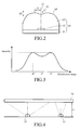
- the first embodiment of the invention is shown in FIGS. 2 and 3. It contains a substrate 21, an LED chip 22, and a lens 23.
- the LED chip 22 is installed on the substrate 21.
- the lens 23 is connected to the substrate 21 by packaging to cover the LED chip 22.
- On the surface of the lens 23 and in the vicinity of the optical axis 24 is formed with a concave part as a divergent surface 25. Beyond the divergent surface 25 is a convergent surface 26.
- the thickness of the divergent surface 25 increases from the optical axis outwards.
- the thickness of the convergent surface 26 decreases from the maximum outward.
- the divergent surface 25 is used to diverge the light near the optical axis 24, it is preferably to use a concave surface. However, it can be a mixture of concave and convex surfaces.
- the convergent surface 26 is used to converge light with large emission angles. Therefore, it is preferably to be a convex surface. As shown in FIG. 4, when projecting light on a screen 70 at a distance of H, the disclosed LED 20 has a larger and more homogeneous light-emitting range, in comparison with the conventional LED 10.
- the homogeneous light-emitting area is about 33 mm from the optical axis according to the first experimental data set.
- the LED chip has a distance of 30 mm. Therefore, we obtain a subtending angle of 47.7 degrees.
- the subtending angle in FIGS. 10A and 10B is 53.8 degrees, that in FIGS. 11A and 11B is 67.4 degrees, and that in FIGS. 12A and 12B is 72.3 degrees.
- the subtending angle is enlarged to 45 to 75 degrees using the invention.
- the lens 30 is designed to be a mask. Its surface also has a divergent surface 32 and a convergent surface 33. Its bottom has a concave part 31 that is greater than the LED chip 22. When the lens 30 is connected to the substrate 21, the concave part 31 covers the LED chip 22. A large-area homogeneous light-emitting area is also obtained.
- FIG. 7 A fourth embodiment is shown in FIG. 7.
- the surface of the lens 40 has the form of a Fresnel lens 42.
- the bottom also has a concave part 41 for accommodating an LED chip 22.
- the equivalent lens of the Fresnel lens-like surface 42 is the same as the above-mentioned lens 23 (see FIG. 2). This design can reduce the thickness of the LED and allow wider applications.
- pluralities of LED's 20 are distributed on the frame 61 of a backlit module.
- a diffusive plate 62 is combined from the top. This can be used in a backlit module because the LED's 20 have better homogeneity and light-emitting range. In comparison with the prior art, the required number of LED's 20 for a backlit module of the same thickness can be reduced. In this case, it is less likely to have focused light spots.
Landscapes
- Physics & Mathematics (AREA)
- General Physics & Mathematics (AREA)
- Optics & Photonics (AREA)
- Engineering & Computer Science (AREA)
- General Engineering & Computer Science (AREA)
- Led Device Packages (AREA)
Abstract
Description
- The invention relates to a lens and a light-emitting diode (LED) using the lens for illumination systems and, in particular, to an LED with homogeneous illumination.
- A
traditional LED 10 is shown in FIG. 1A. It is formed by packing anLED chip 12 in alens 11. The most commonly seen embodiment of the lens is illustrated in the drawing. Thelens 11 is a hemisphere to converge the light emitted by theLED chip 12. The radiation pattern (directions and energy distribution of the emitted light) has to be restricted in the vicinity of theoptical axis 13. Since the energy is more concentrated, one has to rely on the use of a light-guidingplate 14 to improve the homogeneity in the case of a surface plane light source. However, if the LED's 10 are directly distributed under the light-guiding plate, it requires a fair amount of LED's 10 because each one of them has a very small illuminating area. Therefore, one usually adopts the side-illuminating structure to achieve the required homogeneity of a surface plane light source, as shown in FIG. 1B. However, since the LED's 10 can provide the optical energy only at the edge of the light-guidingplate 14, the distance between the central part and the adjacent light sources becomes larger when the area of the surface plane light source is big. Therefore, the optical energy transmitted to the central part by virtue of total reflections become insufficient as the area enlarges. In other words, there is a certain limit for the area of the surface plane light source. - To overcome this problem,
U.S. Pat. No. 6,679,621 uses a special lens shape to totally reflect the light coming out of the top surface of the LED and to deflect the light coming out of its side surfaces. All beams are emitted in parallel but orthogonal to the optical axis. Therefore, in the construction of a planar light surface, the LED's can be disposed in the middle of the light-guiding plate, instead of being limited to its edges. As the area of the surface plane light source gets larger, there will not be any problem of insufficient optical energy on the light-guiding plate due to the far distances to the light source. Nevertheless, the design relies on the total reflection and refraction of light. The overall light-emitting efficiency is lowered due to the attenuation of multiple reflections and refractions inside the light source system. - In view of the foregoing, an object of the invention is to provide a lens and a homogeneously illuminating LED using the lens. The invention can provide a large-area, homogeneous light-emitting surface. It can be directly used in a surface plane light source system. It further reduces the use of LED's to save the cost.
- To achieve the above object, the disclosed lens and the LED that uses the lens have a lens designed on an action surface and in such a way that a concave divergent surface is formed around the optical axis. This design can deflect the light emitted in the vicinity of the optical axis away from the optical axis, so that the LED can provide a homogeneous and large-area light-emitting surface. According to a first embodiment, the invention includes a substrate, an LED chip, and a lens. The lens is bonded onto the substrate by packaging and covers the LED chip. The lens has a divergent surface around the optical axis and an adjacent convergent surface. The divergent surface diverges the light around the optical axis, and the convergent surface converges light of large angles toward the optical axis. Thus, the LED's can provide more homogeneous light in a larger area.
- In a second embodiment of the invention, the lens is designed to have a concave part at its bottom and to be directly connected to the substrate. The concave part covers the LED chip.
- In a third embodiment of the invention, the concave part at the bottom of the lens is designed to be the top surface of a conventional LED. The lens is directly installed on the conventional LED.
- In a fourth embodiment, the lens is in the form of a Fresnel lens. Its equivalent lens is the same as before. However, the thickness of it is reduced to have more practical applications.
- The invention will become more fully understood from the detailed description given hereinbelow illustration only, and thus are not limitative of the present invention, and wherein:
- FIG. 1A is a schematic view of a conventional LED and its light-emitting style.
- FIG. 1B is a schematic view of a conventional backlit module.
- FIG. 2 is a schematic view of the disclosed LED according to the first embodiment of the invention.
- FIG. 3 is a light intensity distribution diagram of the disclosed LED.
- FIG. 4 compares the light-emitting area of the disclosed LED.
- FIG. 5 is a schematic view of the disclosed LED according to the second embodiment of the invention.
- FIG. 6 is a schematic view of the disclosed LED according to the third embodiment of the invention.
- FIG. 7 is a schematic view of the disclosed LED according to the fourth embodiment of the invention.
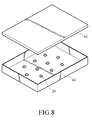
- FIG. 8 shows an application of the invention.
- FIGS. 9A and 9B to 12A and 12B give the experimental data in our simulations.
- In observation of the fact that the conventional LED usually has stronger light intensity around its optical axis, the disclosed lens and the LED using the disclosed lens diverge light in the vicinity of the optical axis. The first embodiment of the invention is shown in FIGS. 2 and 3. It contains a
substrate 21, anLED chip 22, and alens 23. TheLED chip 22 is installed on thesubstrate 21. Thelens 23 is connected to thesubstrate 21 by packaging to cover theLED chip 22. On the surface of thelens 23 and in the vicinity of theoptical axis 24 is formed with a concave part as adivergent surface 25. Beyond thedivergent surface 25 is aconvergent surface 26. The thickness of thedivergent surface 25 increases from the optical axis outwards. The thickness of theconvergent surface 26 decreases from the maximum outward. The upper action surface of thelens 23 is a continuous curved surface. The action surface referred herein means the surface above thelens 23 for the light emitted by theLED chip 22 to deflect. With this action surface, one is able to obtain a large-area and homogeneous beam of light. Therefore, the action surface does not necessarily mean the whole upper surface of thelens 23. It can be only a part of the upper surface. The size of the action surface is determined by the width and height of thelens 23, and type of theLED chip 22. The light emitted by theLED chip 22 and going through thedivergent surface 25 is deflected away from theoptical axis 24, whereas the light emitted by theLED chip 22 and going through theconvergent surface 26 is deflected toward theoptical axis 24. Therefore, the light intensity within a certain range becomes more homogeneous. The light intensity distribution is shown in FIG. 3. As one can see, the maximum intensity region is shifted outward away from theoptical axis 24. The overall light-emitting region is larger and more homogeneous. In particular, the distance to the maximum light intensity region can be adjusted according to the distance d1 from the highest point on the surface of thelens 23 to theoptical axis 24 and the height difference d2 from the lowest point of thedivergent surface 25 to the highest point. A common design is that thelens 23 is a cylinder symmetric about theoptical axis 24. Therefore, the intersection between thedivergent surface 25 and theoptical axis 24 is the lowest point. The distance d1 and the height difference d2 can be adjusted according to the refractive index, temperature coefficient, thickness, and height of the lens, the LED chip, and the desired homogeneous light-emitting area. - Since the
divergent surface 25 is used to diverge the light near theoptical axis 24, it is preferably to use a concave surface. However, it can be a mixture of concave and convex surfaces. Theconvergent surface 26 is used to converge light with large emission angles. Therefore, it is preferably to be a convex surface. As shown in FIG. 4, when projecting light on ascreen 70 at a distance of H, the disclosedLED 20 has a larger and more homogeneous light-emitting range, in comparison with theconventional LED 10. - With reference to FIGS. 9A and 9B, one sees that the homogeneous light-emitting area is about 33 mm from the optical axis according to the first experimental data set. The LED chip has a distance of 30 mm. Therefore, we obtain a subtending angle of 47.7 degrees. Likewise, the subtending angle in FIGS. 10A and 10B is 53.8 degrees, that in FIGS. 11A and 11B is 67.4 degrees, and that in FIGS. 12A and 12B is 72.3 degrees. We therefore see that the subtending angle is enlarged to 45 to 75 degrees using the invention.
- On the other hand, the second embodiment of the invention is shown in FIG. 5. The
lens 30 is designed to be a mask. Its surface also has adivergent surface 32 and aconvergent surface 33. Its bottom has aconcave part 31 that is greater than theLED chip 22. When thelens 30 is connected to thesubstrate 21, theconcave part 31 covers theLED chip 22. A large-area homogeneous light-emitting area is also obtained. - A third embodiment of the invention is shown in FIG. 6. The
concave part 31 is designed according to the shape of theLED 10 so that it can be directly combined with aconventional LED 10. This design is more convenient in use. However, the light-emitting efficiency is slightly lower due to the extra deflection. - A fourth embodiment is shown in FIG. 7. The surface of the
lens 40 has the form of aFresnel lens 42. The bottom also has aconcave part 41 for accommodating anLED chip 22. The equivalent lens of the Fresnel lens-like surface 42 is the same as the above-mentioned lens 23 (see FIG. 2). This design can reduce the thickness of the LED and allow wider applications. - As shown in FIG. 8, pluralities of LED's 20 are distributed on the
frame 61 of a backlit module. Adiffusive plate 62 is combined from the top. This can be used in a backlit module because the LED's 20 have better homogeneity and light-emitting range. In comparison with the prior art, the required number of LED's 20 for a backlit module of the same thickness can be reduced. In this case, it is less likely to have focused light spots. - Certain variations would be apparent to those skilled in the art, which variations are considered within the spirit and scope of the claimed invention.
Claims (23)
- A lens having a circularly symmetric structure and a continuous action surface with a concave part in the middle of its surface, defined as a divergent surface, and a convergent surface around the divergent surface, wherein the thickness of the divergent surface increases outwards whereas the thickness of the convergent surface decreases outwards.
- The lens of claim 1, wherein the divergent surface is a combination of curved surfaces and anti-curved surfaces.
- The lens of claim 1, wherein the convergent surface is a convex surface.
- A light-emitting diode (LED) that emits homogeneous light, comprising:an LED chip, which has an optical axis; anda lens, which has a circularly symmetric structure and covers the LED chip and whose action surface is a continuous curved surface, wherein the action surface in the vicinity of the optical axis has a concave part, defined as a divergent surface, and the divergent surface is surrounded by a convergent surface, the thickness of the divergent surface increases outwards and the thickness of the convergent surface decreases outwards, so that the light emitted from the LED chip is deflected away from the optical axis as it goes through the divergent surface and is deflected toward the optical axis as it goes through the convergent surface.
- The LED of claim 4, wherein the subtending angle of the homogeneous light-emitting range of the LED chip is between 45 degrees and 75 degrees.
- The LED of claim 4, wherein the lowest point on the divergent surface is at the intersection of the optical axis and the divergent surface.
- The LED of claim 4, wherein the divergent surface is a combination of curved and anti-curved surfaces.
- The LED of claim 4, wherein the convergent surface is a convex surface.
- A light-emitting diode (LED) that emits homogeneous light, comprising:a substrate;an LED chip, which is installed on the substrate and has an optical axis; anda lens, whose bottom has a concave part to cover the LED chip when the lens is connected to the substrate and whose action surface is a continuous curved surface, wherein the action surface in the vicinity of the optical axis has a concave part, defined as a divergent surface, and the divergent surface is surrounded by a convergent surface, the thickness of the divergent surface increases outwards and the thickness of the convergent surface decreases outwards, so that the light emitted from the LED chip is deflected away from the optical axis as it goes through the divergent surface and is deflected toward the optical axis as it goes through the convergent surface.
- The LED of claim 9, wherein the subtending angle of the homogeneous light-emitting range of the LED chip is between 45 degrees and 75 degrees.
- The LED of claim 9, wherein the lowest point on the divergent surface is at the intersection of the optical axis and the divergent surface.
- The LED of claim 9, wherein the divergent surface is a combination of curved and anti-curved surfaces.
- The LED of claim 9, wherein the convergent surface is a convex surface.
- A light-emitting diode (LED) that emits homogeneous light, comprising:an LED module, which has an optical axis; anda lens, whose bottom has a concave part to combine with the top part of the LED module and whose action surface is a continuous curved surface,wherein the action surface in the vicinity of the optical axis has a concave part, defined as a divergent surface, and the divergent surface is surrounded by a convergent surface, the thickness of the divergent surface increases outwards and the thickness of the convergent surface decreases outwards, so that the light emitted from the LED chip is deflected away from the optical axis as it goes through the divergent surface and is deflected toward the optical axis as it goes through the convergent surface.
- The LED of claim 14, wherein the subtending angle of the homogeneous light-emitting range of the LED chip is between 45 degrees and 75 degrees.
- The LED of claim 14, wherein the lowest point on the divergent surface is at the intersection of the optical axis and the divergent surface.
- The LED of claim 14, wherein the divergent surface is a combination of curved and anti-curved surfaces.
- The LED of claim 14, wherein the convergent surface is a convex surface.
- A light-emitting diode (LED) that emits homogeneous light, comprising:a substrate;an LED chip, which is installed on the substrate and has an optical axis; anda lens, which is formed on the substrate to cover the LED chip and whose surface is in the form of a Fresnel lens;wherein the action surface of the lens in the vicinity of the optical axis has a concave part, defined as a divergent surface, and the divergent surface is surrounded by a convergent surface, the thickness of the divergent surface increases outwards and the thickness of the convergent surface decreases outwards, so that the light emitted from the LED chip is deflected away from the optical axis as it goes through the divergent surface and is deflected toward the optical axis as it goes through the convergent surface.
- The LED of claim 19, wherein the subtending angle of the homogeneous light-emitting range of the LED chip is between 45 degrees and 75 degrees.
- The LED of claim 19, wherein the lowest point on the divergent surface is at the intersection of the optical axis and the divergent surface.
- The LED of claim 19, wherein the divergent surface is a combination of curved and anti-curved surfaces.
- The LED of claim 19, wherein the convergent surface is a convex surface.
Priority Applications (1)
| Application Number | Priority Date | Filing Date | Title |
|---|---|---|---|
| EP06290844A EP1860467A1 (en) | 2006-05-24 | 2006-05-24 | Lens and light emitting diode using the lens to achieve homogeneous illumination |
Applications Claiming Priority (1)
| Application Number | Priority Date | Filing Date | Title |
|---|---|---|---|
| EP06290844A EP1860467A1 (en) | 2006-05-24 | 2006-05-24 | Lens and light emitting diode using the lens to achieve homogeneous illumination |
Publications (1)
| Publication Number | Publication Date |
|---|---|
| EP1860467A1 true EP1860467A1 (en) | 2007-11-28 |
Family
ID=37908066
Family Applications (1)
| Application Number | Title | Priority Date | Filing Date |
|---|---|---|---|
| EP06290844A Ceased EP1860467A1 (en) | 2006-05-24 | 2006-05-24 | Lens and light emitting diode using the lens to achieve homogeneous illumination |
Country Status (1)
| Country | Link |
|---|---|
| EP (1) | EP1860467A1 (en) |
Cited By (36)
| Publication number | Priority date | Publication date | Assignee | Title |
|---|---|---|---|---|
| US7584534B2 (en) | 2005-01-10 | 2009-09-08 | Perceptron, Inc. | Remote inspection device |
| EP2325907A1 (en) * | 2009-11-20 | 2011-05-25 | LG Innotek Co., Ltd. | Light emitting apparatus |
| EP2378338A1 (en) * | 2010-04-07 | 2011-10-19 | Enplas Corporation | Light flux controlling member, light emitting device, and lighting device |
| CN101839442B (en) * | 2010-01-13 | 2012-06-20 | 浙江耀中科技有限公司 | LED combined optical lens |
| US8434914B2 (en) | 2009-12-11 | 2013-05-07 | Osram Sylvania Inc. | Lens generating a batwing-shaped beam distribution, and method therefor |
| US8506122B2 (en) | 2009-11-19 | 2013-08-13 | Lg Innotek Co., Ltd. | Lens and light emitting apparatus having the same |
| WO2013151224A1 (en) * | 2012-04-05 | 2013-10-10 | Lg Innotek Co., Ltd. | Member for cotrolling luminous flux and display device having the same |
| WO2014011469A1 (en) * | 2012-07-09 | 2014-01-16 | Cree, Inc. | Light emitting diode primary optic for beam shaping |
| EP2790055A1 (en) * | 2013-04-04 | 2014-10-15 | LG Electronics, Inc. | Display apparatus |
| US8905575B2 (en) | 2012-02-09 | 2014-12-09 | Cree, Inc. | Troffer-style lighting fixture with specular reflector |
| US9052075B2 (en) | 2013-03-15 | 2015-06-09 | Cree, Inc. | Standardized troffer fixture |
| USD749768S1 (en) | 2014-02-06 | 2016-02-16 | Cree, Inc. | Troffer-style light fixture with sensors |
| US9285099B2 (en) | 2012-04-23 | 2016-03-15 | Cree, Inc. | Parabolic troffer-style light fixture |
| US9291330B2 (en) | 2009-12-11 | 2016-03-22 | Osram Sylvania Inc. | Retrofit-style lamp and fixture, each including a one-dimensional linear batwing lens |
| US9310038B2 (en) | 2012-03-23 | 2016-04-12 | Cree, Inc. | LED fixture with integrated driver circuitry |
| US9360185B2 (en) | 2012-04-09 | 2016-06-07 | Cree, Inc. | Variable beam angle directional lighting fixture assembly |
| US9423117B2 (en) | 2011-12-30 | 2016-08-23 | Cree, Inc. | LED fixture with heat pipe |
| US9423104B2 (en) | 2013-03-14 | 2016-08-23 | Cree, Inc. | Linear solid state lighting fixture with asymmetric light distribution |
| US9494304B2 (en) | 2012-11-08 | 2016-11-15 | Cree, Inc. | Recessed light fixture retrofit kit |
| US9494294B2 (en) | 2012-03-23 | 2016-11-15 | Cree, Inc. | Modular indirect troffer |
| US9494293B2 (en) | 2010-12-06 | 2016-11-15 | Cree, Inc. | Troffer-style optical assembly |
| USD772465S1 (en) | 2014-02-02 | 2016-11-22 | Cree Hong Kong Limited | Troffer-style fixture |
| US9581312B2 (en) | 2010-12-06 | 2017-02-28 | Cree, Inc. | LED light fixtures having elongated prismatic lenses |
| USD786471S1 (en) | 2013-09-06 | 2017-05-09 | Cree, Inc. | Troffer-style light fixture |
| US9777897B2 (en) | 2012-02-07 | 2017-10-03 | Cree, Inc. | Multiple panel troffer-style fixture |
| US9822951B2 (en) | 2010-12-06 | 2017-11-21 | Cree, Inc. | LED retrofit lens for fluorescent tube |
| USD807556S1 (en) | 2014-02-02 | 2018-01-09 | Cree Hong Kong Limited | Troffer-style fixture |
| US9874322B2 (en) | 2012-04-10 | 2018-01-23 | Cree, Inc. | Lensed troffer-style light fixture |
| US10012354B2 (en) | 2015-06-26 | 2018-07-03 | Cree, Inc. | Adjustable retrofit LED troffer |
| US10054274B2 (en) | 2012-03-23 | 2018-08-21 | Cree, Inc. | Direct attach ceiling-mounted solid state downlights |
| US10309627B2 (en) | 2012-11-08 | 2019-06-04 | Cree, Inc. | Light fixture retrofit kit with integrated light bar |
| US10527225B2 (en) | 2014-03-25 | 2020-01-07 | Ideal Industries, Llc | Frame and lens upgrade kits for lighting fixtures |
| US10544925B2 (en) | 2012-01-06 | 2020-01-28 | Ideal Industries Lighting Llc | Mounting system for retrofit light installation into existing light fixtures |
| US10648643B2 (en) | 2013-03-14 | 2020-05-12 | Ideal Industries Lighting Llc | Door frame troffer |
| US10823347B2 (en) | 2011-07-24 | 2020-11-03 | Ideal Industries Lighting Llc | Modular indirect suspended/ceiling mount fixture |
| US10883702B2 (en) | 2010-08-31 | 2021-01-05 | Ideal Industries Lighting Llc | Troffer-style fixture |
Citations (4)
| Publication number | Priority date | Publication date | Assignee | Title |
|---|---|---|---|---|
| DE8713875U1 (en) * | 1987-10-15 | 1988-02-18 | Siemens Ag, 1000 Berlin Und 8000 Muenchen, De | |
| US20050145867A1 (en) * | 2003-12-26 | 2005-07-07 | Industrial Technology Research Institute | Planar package structure for high power light emitting diode |
| EP1641052A2 (en) * | 2004-09-27 | 2006-03-29 | Enplas Corporation | Emission device, surface light source device, display and light flux control member |
| EP1653254A2 (en) * | 2004-10-18 | 2006-05-03 | Samsung Electronics Co., Ltd. | Light emitting diode and lens for the same |
-
2006
- 2006-05-24 EP EP06290844A patent/EP1860467A1/en not_active Ceased
Patent Citations (4)
| Publication number | Priority date | Publication date | Assignee | Title |
|---|---|---|---|---|
| DE8713875U1 (en) * | 1987-10-15 | 1988-02-18 | Siemens Ag, 1000 Berlin Und 8000 Muenchen, De | |
| US20050145867A1 (en) * | 2003-12-26 | 2005-07-07 | Industrial Technology Research Institute | Planar package structure for high power light emitting diode |
| EP1641052A2 (en) * | 2004-09-27 | 2006-03-29 | Enplas Corporation | Emission device, surface light source device, display and light flux control member |
| EP1653254A2 (en) * | 2004-10-18 | 2006-05-03 | Samsung Electronics Co., Ltd. | Light emitting diode and lens for the same |
Cited By (57)
| Publication number | Priority date | Publication date | Assignee | Title |
|---|---|---|---|---|
| US7584534B2 (en) | 2005-01-10 | 2009-09-08 | Perceptron, Inc. | Remote inspection device |
| US8218074B2 (en) | 2005-01-10 | 2012-07-10 | Perceptron, Inc. | Remote inspection device |
| US8616729B2 (en) | 2009-11-19 | 2013-12-31 | Lg Electronics Inc. | Lens and light emitting apparatus having the same |
| US8506122B2 (en) | 2009-11-19 | 2013-08-13 | Lg Innotek Co., Ltd. | Lens and light emitting apparatus having the same |
| US8395183B2 (en) | 2009-11-20 | 2013-03-12 | Lg Innotek Co., Ltd. | Light emitting apparatus |
| EP2325907A1 (en) * | 2009-11-20 | 2011-05-25 | LG Innotek Co., Ltd. | Light emitting apparatus |
| US10030823B2 (en) | 2009-11-20 | 2018-07-24 | Lg Innotek Co., Ltd. | Light emitting apparatus |
| US9534744B2 (en) | 2009-11-20 | 2017-01-03 | Lg Innotek Co., Ltd. | Light emitting apparatus |
| US8823048B2 (en) | 2009-11-20 | 2014-09-02 | Lg Innotek Co., Ltd. | Light emitting apparatus |
| US9638378B2 (en) | 2009-11-20 | 2017-05-02 | Lg Innotek Co., Ltd. | Light emitting apparatus |
| US9885450B2 (en) | 2009-11-20 | 2018-02-06 | Lg Innotek Co., Ltd. | Light emitting apparatus |
| US8434914B2 (en) | 2009-12-11 | 2013-05-07 | Osram Sylvania Inc. | Lens generating a batwing-shaped beam distribution, and method therefor |
| US9453619B2 (en) | 2009-12-11 | 2016-09-27 | Osram Sylvania Inc. | Retrofit-style lamp and fixture, each including a one-dimensional linear batwing lens |
| US9291330B2 (en) | 2009-12-11 | 2016-03-22 | Osram Sylvania Inc. | Retrofit-style lamp and fixture, each including a one-dimensional linear batwing lens |
| CN101839442B (en) * | 2010-01-13 | 2012-06-20 | 浙江耀中科技有限公司 | LED combined optical lens |
| US8613532B2 (en) | 2010-04-07 | 2013-12-24 | Enplas Corporation | Light flux controlling member, light emitting device, and lighting device |
| EP2378338A1 (en) * | 2010-04-07 | 2011-10-19 | Enplas Corporation | Light flux controlling member, light emitting device, and lighting device |
| US10883702B2 (en) | 2010-08-31 | 2021-01-05 | Ideal Industries Lighting Llc | Troffer-style fixture |
| US11306895B2 (en) | 2010-08-31 | 2022-04-19 | Ideal Industries Lighting Llc | Troffer-style fixture |
| US9822951B2 (en) | 2010-12-06 | 2017-11-21 | Cree, Inc. | LED retrofit lens for fluorescent tube |
| US9494293B2 (en) | 2010-12-06 | 2016-11-15 | Cree, Inc. | Troffer-style optical assembly |
| US9581312B2 (en) | 2010-12-06 | 2017-02-28 | Cree, Inc. | LED light fixtures having elongated prismatic lenses |
| US10823347B2 (en) | 2011-07-24 | 2020-11-03 | Ideal Industries Lighting Llc | Modular indirect suspended/ceiling mount fixture |
| US11209135B2 (en) | 2011-07-24 | 2021-12-28 | Ideal Industries Lighting Llc | Modular indirect suspended/ceiling mount fixture |
| US9423117B2 (en) | 2011-12-30 | 2016-08-23 | Cree, Inc. | LED fixture with heat pipe |
| US10544925B2 (en) | 2012-01-06 | 2020-01-28 | Ideal Industries Lighting Llc | Mounting system for retrofit light installation into existing light fixtures |
| US11408569B2 (en) | 2012-01-06 | 2022-08-09 | Ideal Industries Lighting Llc | Mounting system for retrofit light installation into existing light fixtures |
| US9777897B2 (en) | 2012-02-07 | 2017-10-03 | Cree, Inc. | Multiple panel troffer-style fixture |
| US8905575B2 (en) | 2012-02-09 | 2014-12-09 | Cree, Inc. | Troffer-style lighting fixture with specular reflector |
| US9494294B2 (en) | 2012-03-23 | 2016-11-15 | Cree, Inc. | Modular indirect troffer |
| US9310038B2 (en) | 2012-03-23 | 2016-04-12 | Cree, Inc. | LED fixture with integrated driver circuitry |
| US10514139B2 (en) | 2012-03-23 | 2019-12-24 | Ideal Industries, Llc | LED fixture with integrated driver circuitry |
| US10054274B2 (en) | 2012-03-23 | 2018-08-21 | Cree, Inc. | Direct attach ceiling-mounted solid state downlights |
| US9606399B2 (en) | 2012-04-05 | 2017-03-28 | Lg Innotek Co., Ltd. | Member for controlling luminous flux and display device having the same |
| WO2013151224A1 (en) * | 2012-04-05 | 2013-10-10 | Lg Innotek Co., Ltd. | Member for cotrolling luminous flux and display device having the same |
| KR101417258B1 (en) | 2012-04-05 | 2014-07-08 | 엘지이노텍 주식회사 | Member for controlling luminous flux and display device having the same |
| US9360185B2 (en) | 2012-04-09 | 2016-06-07 | Cree, Inc. | Variable beam angle directional lighting fixture assembly |
| US9874322B2 (en) | 2012-04-10 | 2018-01-23 | Cree, Inc. | Lensed troffer-style light fixture |
| US9285099B2 (en) | 2012-04-23 | 2016-03-15 | Cree, Inc. | Parabolic troffer-style light fixture |
| WO2014011469A1 (en) * | 2012-07-09 | 2014-01-16 | Cree, Inc. | Light emitting diode primary optic for beam shaping |
| US8931929B2 (en) | 2012-07-09 | 2015-01-13 | Cree, Inc. | Light emitting diode primary optic for beam shaping |
| US10309627B2 (en) | 2012-11-08 | 2019-06-04 | Cree, Inc. | Light fixture retrofit kit with integrated light bar |
| US9494304B2 (en) | 2012-11-08 | 2016-11-15 | Cree, Inc. | Recessed light fixture retrofit kit |
| US10648643B2 (en) | 2013-03-14 | 2020-05-12 | Ideal Industries Lighting Llc | Door frame troffer |
| US9423104B2 (en) | 2013-03-14 | 2016-08-23 | Cree, Inc. | Linear solid state lighting fixture with asymmetric light distribution |
| US9052075B2 (en) | 2013-03-15 | 2015-06-09 | Cree, Inc. | Standardized troffer fixture |
| US10228111B2 (en) | 2013-03-15 | 2019-03-12 | Cree, Inc. | Standardized troffer fixture |
| EP2790055A1 (en) * | 2013-04-04 | 2014-10-15 | LG Electronics, Inc. | Display apparatus |
| US9303845B2 (en) | 2013-04-04 | 2016-04-05 | Lg Electronics Inc. | Display apparatus |
| USD786471S1 (en) | 2013-09-06 | 2017-05-09 | Cree, Inc. | Troffer-style light fixture |
| USD772465S1 (en) | 2014-02-02 | 2016-11-22 | Cree Hong Kong Limited | Troffer-style fixture |
| USRE48620E1 (en) | 2014-02-02 | 2021-07-06 | Ideal Industries Lighting Llc | Troffer-style fixture |
| USD807556S1 (en) | 2014-02-02 | 2018-01-09 | Cree Hong Kong Limited | Troffer-style fixture |
| USRE49228E1 (en) | 2014-02-02 | 2022-10-04 | Ideal Industries Lighting Llc | Troffer-style fixture |
| USD749768S1 (en) | 2014-02-06 | 2016-02-16 | Cree, Inc. | Troffer-style light fixture with sensors |
| US10527225B2 (en) | 2014-03-25 | 2020-01-07 | Ideal Industries, Llc | Frame and lens upgrade kits for lighting fixtures |
| US10012354B2 (en) | 2015-06-26 | 2018-07-03 | Cree, Inc. | Adjustable retrofit LED troffer |
Similar Documents
| Publication | Publication Date | Title |
|---|---|---|
| EP1860467A1 (en) | Lens and light emitting diode using the lens to achieve homogeneous illumination | |
| US7582913B2 (en) | Lens and LED using the lens to achieve homogeneous illumination | |
| US7034343B1 (en) | Dipolar side-emitting LED lens and LED module incorporating the same | |
| KR102257061B1 (en) | Multibeam diffraction grating-based color backlighting | |
| KR100468860B1 (en) | Light guide panel having light deflection member and edge light type backlight apparatus | |
| JP4546579B1 (en) | Lighting lens, light emitting device, surface light source, and liquid crystal display device | |
| JP6235491B2 (en) | Optical element for uniform illumination | |
| US9249950B2 (en) | Illumination device for providing the maximum illumination effect | |
| US10352529B2 (en) | Collimating optic for LED illumination assembly having transverse slots on emission surface | |
| JP5342939B2 (en) | Lighting lens, light emitting device, surface light source, and liquid crystal display device | |
| JP2009542017A (en) | Optoelectronic components and lighting equipment | |
| JPWO2013035788A1 (en) | Lighting device and lighting stand | |
| EP2279374B1 (en) | Optical element for asymmetric light distribution | |
| US20150009683A1 (en) | Lens Plate For Illumination Lamp, and Illumination Lamp | |
| JP5118617B2 (en) | Lighting lens, light emitting device, surface light source, and liquid crystal display device | |
| US20150292712A1 (en) | Display Device | |
| CN103912823A (en) | Backlight assembly and a display device using the same | |
| US20060202218A1 (en) | Light-emitting diode for decoration | |
| JP2006332638A (en) | Light emitting diode apparatus | |
| JP2010186142A (en) | Lens for illumination, light emitter, surface light source, and liquid crystal display device | |
| US20130033874A1 (en) | Light-emitting apparatus and lighting system | |
| JP7024399B2 (en) | Light source unit and lighting equipment | |
| TWI392125B (en) | Light emitting device | |
| KR101583647B1 (en) | Light Guide Lens for LED | |
| US20090129095A1 (en) | Illumination system |
Legal Events
| Date | Code | Title | Description |
|---|---|---|---|
| PUAI | Public reference made under article 153(3) epc to a published international application that has entered the european phase |
Free format text: ORIGINAL CODE: 0009012 |
|
| 17P | Request for examination filed |
Effective date: 20060603 |
|
| AK | Designated contracting states |
Kind code of ref document: A1 Designated state(s): AT BE BG CH CY CZ DE DK EE ES FI FR GB GR HU IE IS IT LI LT LU LV MC NL PL PT RO SE SI SK TR |
|
| AX | Request for extension of the european patent |
Extension state: AL BA HR MK YU |
|
| AKX | Designation fees paid |
Designated state(s): DE FR GB |
|
| 17Q | First examination report despatched |
Effective date: 20080730 |
|
| STAA | Information on the status of an ep patent application or granted ep patent |
Free format text: STATUS: THE APPLICATION HAS BEEN REFUSED |
|
| 18R | Application refused |
Effective date: 20111013 |