EP1814039A2 - Vorrichtung, System und Verfahren für ein Kohärenzschema eines Mehrzustands-Cachespeichers - Google Patents
Vorrichtung, System und Verfahren für ein Kohärenzschema eines Mehrzustands-Cachespeichers Download PDFInfo
- Publication number
- EP1814039A2 EP1814039A2 EP20060256444 EP06256444A EP1814039A2 EP 1814039 A2 EP1814039 A2 EP 1814039A2 EP 20060256444 EP20060256444 EP 20060256444 EP 06256444 A EP06256444 A EP 06256444A EP 1814039 A2 EP1814039 A2 EP 1814039A2
- Authority
- EP
- European Patent Office
- Prior art keywords
- memory
- cache
- processor
- coherence state
- cache coherence
- Prior art date
- Legal status (The legal status is an assumption and is not a legal conclusion. Google has not performed a legal analysis and makes no representation as to the accuracy of the status listed.)
- Ceased
Links
Images

Classifications
-
- G—PHYSICS
- G06—COMPUTING; CALCULATING OR COUNTING
- G06F—ELECTRIC DIGITAL DATA PROCESSING
- G06F12/00—Accessing, addressing or allocating within memory systems or architectures
- G06F12/02—Addressing or allocation; Relocation
- G06F12/08—Addressing or allocation; Relocation in hierarchically structured memory systems, e.g. virtual memory systems
- G06F12/0802—Addressing of a memory level in which the access to the desired data or data block requires associative addressing means, e.g. caches
- G06F12/0806—Multiuser, multiprocessor or multiprocessing cache systems
- G06F12/0815—Cache consistency protocols
- G06F12/0831—Cache consistency protocols using a bus scheme, e.g. with bus monitoring or watching means
-
- G—PHYSICS
- G06—COMPUTING; CALCULATING OR COUNTING
- G06F—ELECTRIC DIGITAL DATA PROCESSING
- G06F9/00—Arrangements for program control, e.g. control units
- G06F9/06—Arrangements for program control, e.g. control units using stored programs, i.e. using an internal store of processing equipment to receive or retain programs
- G06F9/46—Multiprogramming arrangements
-
- G—PHYSICS
- G06—COMPUTING; CALCULATING OR COUNTING
- G06F—ELECTRIC DIGITAL DATA PROCESSING
- G06F12/00—Accessing, addressing or allocating within memory systems or architectures
-
- G—PHYSICS
- G06—COMPUTING; CALCULATING OR COUNTING
- G06F—ELECTRIC DIGITAL DATA PROCESSING
- G06F12/00—Accessing, addressing or allocating within memory systems or architectures
- G06F12/02—Addressing or allocation; Relocation
- G06F12/08—Addressing or allocation; Relocation in hierarchically structured memory systems, e.g. virtual memory systems
- G06F12/0802—Addressing of a memory level in which the access to the desired data or data block requires associative addressing means, e.g. caches
- G06F12/0806—Multiuser, multiprocessor or multiprocessing cache systems
- G06F12/0811—Multiuser, multiprocessor or multiprocessing cache systems with multilevel cache hierarchies
-
- G—PHYSICS
- G06—COMPUTING; CALCULATING OR COUNTING
- G06F—ELECTRIC DIGITAL DATA PROCESSING
- G06F12/00—Accessing, addressing or allocating within memory systems or architectures
- G06F12/02—Addressing or allocation; Relocation
- G06F12/08—Addressing or allocation; Relocation in hierarchically structured memory systems, e.g. virtual memory systems
- G06F12/0802—Addressing of a memory level in which the access to the desired data or data block requires associative addressing means, e.g. caches
- G06F12/0806—Multiuser, multiprocessor or multiprocessing cache systems
- G06F12/0815—Cache consistency protocols
Definitions
- a computing platform may include one or more processor cores, which may be connected to one or more memory units, e.g., a level-1 cache memory and a level-2 cache memory.
- processor cores may be connected to one or more memory units, e.g., a level-1 cache memory and a level-2 cache memory.
- a first processor core may be connected to a first, private, level-1 cache memory
- a second processor core may be connected to a second, private, level-1 cache memory
- the first and second level-1 cache memories may be connected to a shared level-2 cache memory.
- a memory line of a memory unit may have, at a certain time point, a single cache coherence state out of multiple possible cache coherence states, for example, either a modified ("M") state, an owned (“O") state, an exclusive (“E”) state, a shared (“S”) state, or an invalid (“I”) state.
- a memory line may have a shared state, indicating that the memory line may be shared internally within sub-units of a processing unit, as well as externally with other components of the computing platform.
- Embodiments of the invention may be used in a variety of applications. Although embodiments of the invention are not limited in this regard, embodiments of the invention may be used in conjunction with many apparatuses, for example, a computer, a computing platform, a personal computer, a desktop computer, a mobile computer, a laptop computer, a notebook computer, a Personal Digital Assistant (PDA) device, a tablet computer, a server computer, a network, a wireless device, a wireless station, a wireless communication device, or the like. Embodiments of the invention may be used in various other apparatuses, devices, systems and/or networks.
- PDA Personal Digital Assistant
- the terms “plurality” and/or “a plurality” as used herein may include, for example, “multiple” or “two or more”.
- the terms “plurality” and/or “a plurality” may be used herein describe two or more components, devices, elements, parameters, or the like.
- a plurality of processors may include two or more processors.
- memory block may include, for example, one or more memory lines, one or more memory addresses, one or more memory portions, one or more memory banks, one or more memory sub-units, one or more memory records or fields, or the like.
- non-cache memory memory units or storage units which may be external or internal to a processor or a processing unit, memory units or storage units which may be external or internal to a motherboard or a computing platform, internal memory, external memory, graphics memory, on-board memory, extended memory, memory included in or associated with a graphics processing card or graphics rendering card, memory included in or associated with a three-dimension (3D) graphics processing card or graphics rendering card, video memory, temporary memory, buffers, registers, accumulators, volatile memory, non-volatile memory, private cache or memory, a non-private cache or memory, shared cache, short-term memory, long-term memory, reference memory, intermediate memory, a data cache or memory, an instructions cache or memory, a data/instructions cache or memory,
- portions of the discussion herein may relate, for demonstrative purposes, to a processing unit having two levels of cache, e.g., level-1 cache and level-2 cache, embodiments of the invention are not limited in this respect, and may be used in conjunction with processing units and/or computing platforms utilizing other numbers of cache levels, e.g., more than two cache levels.
- some cache memories and/or memory units which may be used in conjunction of embodiments of the invention may include, for example, one or more or a combination of: a Random Access Memory (RAM), a main RAM, a Static RAM (SRAM), a Dynamic RAM (DRAM), a Burst Static RAM (BS-RAM), a SyncBurst RAM (BS-RAM), a Fast Page Mode DRAM (FPM-DRAM), an Enhanced DRAM (EDRAM), and Extended Data Output RAM (EDO-RAM), an EDO-DRAM, a Burst Extended Data Output DRAM (BEDO-DRAM), a Non-Volatile RAM (NV-RAM), a Synchronous DRAM (SD-RAM), a Joint Electron Device Engineering Council SD-RAM (JEDEC SD-RAM), a PC100 SD-RAM, a Double Data Rate SD-RAM (DDR SD-RAM), an Enhanced SD-RAM (ESD-RAM), a Direct Rambus DRAM (DRD-
- RAM Random Access Memory
- main RAM main RAM
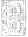
- FIG. 1 schematically illustrates a computing platform 100 utilizing a multi-state cache coherence scheme in accordance with an embodiment of the invention.
- Computing platform 100 may include, for example, an input unit 161, an output unit 162, a storage unit 163, and a main memory unit 150.
- Computing platform 100 may further include one or more processors, processing units, or Chip-level MultiProcessing (CMP) units, e.g., processing clusters 101 and 102.
- CMP Chip-level MultiProcessing
- Computing platform 100 may include other suitable hardware components and/or software components.
- Input unit 161 may include, for example, a keyboard, a keypad, a mouse, a touch-pad, or other suitable pointing device or input device.
- Output unit 162 may include, for example, a screen, a monitor, a speaker, a Cathode Ray Tube (CRT) monitor or display unit, a Liquid Crystal Display (LCD) monitor or display unit, or other suitable monitor or display unit.
- Storage unit 163 may include, for example, a hard disk drive, a floppy disk drive, a Compact Disk (CD) drive, a CD-ROM drive, or other suitable removable or non-removable storage units.
- Memory unit 150 may include, for example, a Random Access Memory (RAM), a Read Only Memory (ROM), a Dynamic RAM (DRAM), a Synchronous DRAM (SD-RAM), a Flash memory, a volatile memory, a non-volatile memory, a cache memory, a buffer, a short term memory unit, a long term memory unit, or other suitable memory units or storage units.
- RAM Random Access Memory
- ROM Read Only Memory
- DRAM Dynamic RAM
- SD-RAM Synchronous DRAM
- Flash memory a volatile memory, a non-volatile memory, a cache memory, a buffer, a short term memory unit, a long term memory unit, or other suitable memory units or storage units.
- Processing cluster 101 may include, for example, a Central Processing Unit (CPU), a Digital Signal Processor (DSP), a microprocessor, a controller, a chip, a microchip, an Integrated Circuit (IC), or any other suitable multi-purpose or specific processor or controller.
- processing cluster 101 may include one or more processors or processor cores, e.g., processor cores 111 and 112.
- processor core 111 may be connected to a private level-1 cache memory 121
- processor core 112 may be connected to a private level-1 cache memory 122.
- Level-1 cache memories 121 and 122 may be connected to a level-2 cache memory 131, optionally through a local interconnect 141, e.g., a bus or point-to-point interconnect..
- processing cluster 102 may include, for example, a Central Processing Unit (CPU), a Digital Signal Processor (DSP), a microprocessor, a controller, a chip, a microchip, an Integrated Circuit (IC), or any other suitable multi-purpose or specific processor or controller.
- processing cluster 102 may include one or more processors or processor cores, e.g., processor cores 113 and 114.
- Processor core 113 may be connected to a private level-1 cache memory 123
- processor core 114 may be connected to a private level-1 cache memory 124.
- Level-1 cache memories 123 and 124 may be connected to a level-2 cache memory 132, optionally through a local interconnect 142, e.g., a bus or point-to-point interconnect.
- Level-2 cache memory 131 of processing cluster 101, and level-2 cache memory 132 of processing cluster 102 may be connected to main memory unit 150, optionally through a global interconnect 143, e.g., a global bus, a system bus, a point-to-point interconnect, or the like.
- Computing platform 100 may optionally include one or more Cache Control Logic (CCL) components or modules, for example, a CCL 191 associated with or included in processing cluster 101, a CCL 192 associated with or included in processing cluster 102, a CCL 193 associated with main memory unit 150 and/or other components external to processing clusters 101-102, or the like.
- CCL Cache Control Logic
- CCLs 191, 192 and/or 193 may be implemented using one or more hardware components and/or software components, using a dedicated unit, as a sub-unit of one or more components of computing platform 100, using a driver, using a general or dedicated controller or processor, using an Integrated Circuit (IC), or the like.
- the functionality of CCLs 191, 192 and/or 193 may be implemented using a directory-based cache logic, using a snooping-based cache logic, or the like.
- Level-1 cache memories 121, 122, 123 and 124, level-2 cache memories 131 and 132, and/or main memory unit 150 may include, or may be operatively associated with, one or more identifiers of Cache Coherency State (CCS).
- the CCS identifier(s) may include data identifying the CCS associated with, or corresponding to, one or more memory blocks.
- the CCS identifier(s) may optionally include, or may be implemented as part of, a memory unit, a memory manager, a memory controller, a circuit or sub-circuit, a logic controller, one or more pointers, one or more tables, one or more data items, or the like.
- level-1 cache memories 121-124 may include, or may be associated with, CCS identifiers 171-174, respectively; level-2 cache memories 131-132 may include, or may be associated with, CCS identifiers 181-182, respectively; and main memory unit 150 may include, or may be associated with, a CCS identifier 151.
- a memory block may have multiple, e.g., different, CCSs vis-à-vis or with respect to one or more other components of computing platform 100.
- a memory block may have a first CCS vis-à-vis or with respect to a first component of computing platform 100, and a second, different, CCS vis-à-vis or with respect to a second, different, component of computing platform 100.
- memory block may substantially simultaneously have multiple CCS such as, for example, a modified ("M") state, a shared (“S”) state, an exclusive (“E”) state, an invalid (“I”) state, and/or other suitable CCS values, e.g., vis-à-vis or with respect to various components of computing platform 100.
- CCSs 191, 192 and/or 193, or other components of computing platform 100 may be used to set or modify a CCS of a memory block of computing platform 100.
- CCS identifier 181 of level-2 cache 131 may substantially simultaneously include two indications: a first indication that a memory block of level-2 cache 131 has a "modified" CCS vis-à-vis or with respect to main memory unit 150 and/or processing cluster 102; and a second indication that that memory block of level-2 cache 131 further has a "shared" CCS vis-à-vis or with respect to level-1 cache memories 121-122 and/or processor cores 111-112.
- the multiple CCSs may be set and/or modified, for example, by CCLs 191, 192 and/or 193, or other components of computing platform 100.
- one or more CCS identifiers in computing platform 100 may include indications of multiple substantially-simultaneous CCSs, whereas one or more other CCS identifiers in computing platform 100 may include indications of single CCSs.
- level-2 cache memory 131 may substantially simultaneously have two CCS, e.g., a "modified” CCS towards, or in relation to or vis-à-vis, main memory 150 and a "shared” CCS towards or in relation to level-1 caches 121-122; whereas level-1 cache memory 111 may have a single CCS, e.g., a "shared” CCS, towards, or in relation to or vis-à-vis, both level-2 cache 131 and processor core 111, and main memory unit 150 may have a single CCS, e.g., a "modified” CCS.
- the various CCSs may be set and/or modified, for example, by CCLs 191, 192 and/or 193, or other components of computing platform 100.
- a memory block of a memory component of computing platform 100 may substantially simultaneously have a first CCS vis-à-vis or with respect to component(s) connected between that memory component and a processor core (i.e., a first CCS "towards the processor core", in the direction of the processor core, a "downlink” CCS, an "internal” CCS, or a downward-looking CCS); and a second, different, CCS vis-à-vis or with respect to component(s) that are not connected between that memory component and the processor core (i.e., a second, different, CCS "away from the processor core", in a direction substantially opposite to the direction of the processor core, in a direction different than the direction of the processor core, an "uplink” CCS, an "external” CCS, or an upward-looking CCS).
- level-2 cache memory 131 may substantially simultaneously have a first CCS, e.g., a "shared” CCS, towards processor cores 111-112; and a second, different CCS, e.g., a "modified” CCS, away from processor cores 111-112.
- the multiple or various CCSs may optionally be set and/or modified, for example, by CCLs 191, 192 and/or 193, or other components of computing platform 100.
- a memory block of a memory component of computing platform 100 may substantially simultaneously have a first CCS vis-à-vis or with respect to component(s) having a first hierarchy, e.g., a hierarchy higher than the hierarchy of the memory component, a "parent" component, or a component located at a higher branch; and a second, different, CCS vis-à-vis or with respect to component(s) having a second, different, hierarchy, e.g., a hierarchy lower than the hierarchy of the memory component, a "child” component, or a component located at a lower branch.
- the multiple or various CCSs may optionally be set and/or modified, for example, by CCLs 191, 192 and/or 193, or other components of computing platform 100.
- a memory block of a memory component of computing platform 100 may substantially simultaneously have a first, local CCS, and a second, global, CCS.
- the local CCS may be, for example, vis-à-vis or with respect to components located in proximity to the memory component, vis-à-vis or with respect to components located in the same processing cluster of the memory component, vis-à-vis or with respect to components having a direct connection or a local connection with the memory component, vis-à-vis or with respect to components that are connected to the memory component not using a bus or a point-to-point interconnect, or the like.
- the global CCS may be, for example, vis-à-vis or with respect to components located on a card or die separate from the memory component, vis-à-vis or with respect to components located on a chip or physical unit separate from the memory component, vis-à-vis or with respect to components that are connected to the memory component using a bus or a point-to-point interconnect, or the like.
- level-2 cache memory 131 may substantially simultaneously have a first, local, CCS, e.g., a "shared" CCS, towards or in relation to processor cores 111-112 or local interconnect 141; and a second, global, CCS, e.g., a "modified" CCS, towards or in relation to global interconnect 143 or processing cluster 102.
- the multiple or various CCSs may optionally be set and/or modified, for example, by CCLs 191, 192 and/or 193, or other components of computing platform 100.
- a memory line of level-1 caches 121-122 may have a "shared” CCS, e.g., the memory line may be read-shared among processor cores 111-112.
- a corresponding memory line of level-2 cache 131 may have a "shared” downward-looking CCS, and may further have a "modified” upward-looking CCS.
- a directory in main memory unit 150, or CCS identifier 151, may indicate that the corresponding memory line has a "modified” CCS and is "owned” by processing cluster 101.
- level-2 cache 132 of processing cluster 102 and/or level-1 caches 123-124 of processing cluster 102 may include, or may be associated with, a CCS identifier indicating that the corresponding memory line has an "invalid" CCS.
- main memory unit 150, and/or components of processing cluster 102 regard the level-2 cache 131 as a cache having a "modified" state, regardless of the possibility that level-2 cache 131 may have a different CCS, e.g., may be read-shared among processor cores 111-112.
- processor core 113 of processing cluster 102 may request to access the memory line of level-2 cache having an "invalid" CCS; in response, the corresponding copies in private level-1 caches 121-122 of processing cluster 101 may be invalidated, and the requested memory line may be forwarded to processor core 113 of processing cluster 102.
- Some embodiments may be used in conjunction with one or more cache coherence protocols, for example, a Modified - Owned - Exclusive - Shared - Invalid (MOESI) protocol, a Modified - Exclusive - Shared - Invalid (MESI) protocol, a Modified - Shared - Invalid (MSI) protocol, or the like.
- MOESI Modified - Owned - Exclusive - Shared - Invalid
- MEMI Modified - Exclusive - Shared - Invalid
- MSI Modified - Shared - Invalid
- a memory component may utilize a first cache coherence protocol to communicate with a first set of components, e.g., local components, components at a lower branch or hierarchy, components at a first level, or the like; and may substantially simultaneously utilize a second, different, cache coherence protocol to communicate with a second set of components, e.g., global components, components at a higher branch or hierarchy, components at a second level, or the like.
- a first cache coherence protocol to communicate with a first set of components, e.g., local components, components at a lower branch or hierarchy, components at a first level, or the like
- a second, different, cache coherence protocol may be used at multiple branches which may be at the same level.
- one or more cache coherence rules or cache coherence definitions may be used, for example, to implement cache coherence architecture in accordance with embodiments of the invention.
- a cache coherence rule may indicate that a memory line may have a global "shared” CCS if the memory line has a "shared” CCS or an "invalid' CCS in substantially all cache memories of a processing cluster, e.g., in caches 121, 122 and 131 of processing cluster 101.
- Another cache coherence rule may indicate that a memory line may have a local "shared” CCS if the memory line has an "exclusive” or “modified” CCS in level-2 cache 131 and further has a "shared” or “invalid” CCS in level-1 caches 121-122.
- Yet another cache coherence rule may indicate that a memory line may be exclusively owned by a processing cluster 101 if at least one of its caches (e.g., caches 121, 122 and 131) identifies that memory line as having an "exclusive” or "modified” CCS.
- Still another cache coherence rule may indicate that a memory line of a first memory component may have a "shared" CCS only internally or locally, e.g., downward-looking towards a processor core, if a corresponding memory line of a higher-level cache has an "exclusive” or “modified” CCS; whereas the memory line may have a global or external "shared” CCS, e.g., upward-looking away from the processor core, if a corresponding memory line of a higher-level cache has a "shared” CCS.
- Other suitable rules or definitions may be used in accordance with embodiments of the invention.
- one or more rules or definitions may be set, modified, and/or utilized, for example, by CCLs 191, 192 and/or 193, or other components of computing platform 100.
- a memory line of level-2 cache 131 may substantially simultaneously have an internal CCS of "shared” towards or in relation to level-1 caches 121-122, and an external CCS of "exclusive” towards or in relation to main memory unit 150 and/or processing cluster 101.
- Such architecture may replace, for example, a single CCS of "shared” towards or in relation to all components of computing platform 101.
- this architecture may obviate a need to send a Request For Ownership (RFO) indication to components external to processing cluster 101, and optionally may obviate a need to receive responses from such external components that their corresponding memory line(s) are invalidated.
- RFO Request For Ownership
- Some embodiments may, for example, reduce the used bandwidth (e.g., of interconnect 143), improve performance, and allow an internal, fast RFO among internal caches, e.g., among level-1 caches 121-122.
- processing core 111 may perform "snooping" operations with respect to processing core 112, e.g., upon or substantially together with accessing level-2 cache 131.
- processing core 111 may access the level-2 cache 131, and may send to processing core 112 a coherence request, e.g., a directory-based coherence request or a snooping-based coherence request.
- the coherence request may include, for example, information about the operation that processor core 111 performs with respect to the level-2 cache 131 (e.g., "processor 111 performs a read operation on memory line 345" or "processor 111 performs a write operation on memory line 567"); and/or information about operations that processor 112 is requested or required to perform (e.g., "processor 112 is allowed to read from memory line 789 but is not allowed to write to memory line 789", or "processor 112 is required to invalidate its memory line 456").
- the coherence request may include, for example, one or more attributes, types, characteristics and/or properties related to the access of the memory line by the processor core 111.
- processor core 111 need not wait for a response to the coherence request that processor 111 sends to one or more other processors, and may perform the reported operation substantially together with sending the coherence request, or immediately subsequent to sending the coherence request.
- processor core 112 may send to processor 111 a coherence response (e.g., directory-based or "snooping"-based), may modify its operation based on the received coherence request, may perform one or more operations or instructions indicated by the received coherence request, may invalidate one or more memory lines, or the like.
- a coherence response e.g., directory-based or "snooping"-based
- CCLs 191, 192 and/or 193 may be utilized to manage, control, store, track and/or transfer cache coherence requests and/or cache coherence responses.
- associating a memory line with more than one CCS may be performed in various suitable ways, e.g., not necessarily utilizing a CCS identifier indicating that the memory line has two or multiple CCSs.
- a memory line in a first memory unit e.g., level-1 cache memory 121
- a memory line in a second memory unit e.g., level-2 cache memory 131
- a final or combined CCS may be reported to external components (e.g., to main memory unit 150) based on a composition of the first CCS and the second CCS, or otherwise based on a calculation that takes into account the first CCS and the second CCS.
- snooping-based queries, responses, instructions and/or data items may be utilized.
- multiple CCSs of a memory line may coincide or overlap.
- a memory line may have a first CCS in relation to a first component, and a second CCS in relation to a second component; the first CCS may, in some cases, be similar or substantially identical to the second CCS, or a single CCS in relation to the first and second components may replace the first and second separate CCSs.
- FIG. 2 is a schematic flow-chart of a method of managing multiple cache coherence states in accordance with an embodiment of the invention. Operations of the method may be implemented, for example, by computing platform 100 of FIG. 1 or by components thereof, by CCLs 191, 192 and/or 193 of FIG. I, and/or by other suitable computers, processors, components, devices, and/or systems.
- the method may optionally include, for example, associating a memory line of a memory unit, e.g., substantially simultaneously, with a first CCS towards or in relation to a first component or set of components of a computing platform, and with a second, different, CCS towards or in relation to a second, different, component or set of components of the computing platform.
- this may be performed utilizing CCLs 191, 192 and/or 193 of FIG. 1, utilizing a directory-based cache coherence protocol, using a snooping-based cache coherence protocol, using one or more CCS identifiers associated with memory lines or memory blocks, or the like.
- the method may optionally include, for example, sending a coherence request, e.g., between processors of the computing platform upon or together with accessing a memory line.
- This may include, for example, sending a coherence request having a representation of an operation that a first processor performs or is about to perform with respect to the memory line, a representation of a type of access that the first processor performs or is about to perform with respect to the memory line, a representation of an operation that a second processor is requested to perform, a representation of a CCS modification that the second processor is requested to perform, or the like.
- the method may optionally include, for example, modifying at least one of the first and second CCSs of a memory line.
- a first CCS associated with a memory line towards or in relation to a first component may be modified, whereas a second, substantially simultaneous, CCS associated with the memory line towards or in relation to a second component may be maintained, e.g., unmodified.
- this may be performed utilizing CCLs 191, 192 and/or 193 of FIG. 1, utilizing a directory-based cache coherence protocol, using a snooping-based cache coherence protocol, using one or more CCS identifiers associated with memory lines or memory blocks, or the like.
- a memory block may substantially simultaneously have more than two (e.g., three, four, five, etc.) different CCSs vis-à-vis or with respect to various components or sets of components.
- a dual-state cache coherence scheme a triple-state cache coherence scheme, a quadruple-state cache coherence scheme, or other multiple-state cache coherence scheme may be used.
- Embodiments of the invention may be implemented by software, by hardware, or by any combination of software and/or hardware as may be suitable for specific applications or in accordance with specific design requirements.
- Embodiments of the invention may include units and/or sub-units, which may be separate of each other or combined together, in whole or in part, and may be implemented using specific, multi-purpose or general processors or controllers, or devices as are known in the art.
- Some embodiments of the invention may include buffers, registers, stacks, storage units and/or memory units, for temporary or long-term storage of data or in order to facilitate the operation of a specific embodiment.
- Some embodiments of the invention may be implemented, for example, using a machine-readable medium or article which may store an instruction or a set of instructions that, if executed by a machine, for example, by processing clusters 101 or 102 of FIG. I, by other suitable machines, cause the machine to perform a method and/or operations in accordance with embodiments of the invention.
- Such machine may include, for example, any suitable processing platform, computing platform, computing device, processing device, computing system, processing system, computer, processor, or the like, and may be implemented using any suitable combination of hardware and/or software.
- the machine-readable medium or article may include, for example, any suitable type of memory unit (e.g., memory unit 150), memory device, memory article, memory medium, storage device, storage article, storage medium and/or storage unit, for example, memory, removable or non-removable media, erasable or non-erasable media, writeable or re-writeable media, digital or analog media, hard disk, floppy disk, Compact Disk Read Only Memory (CD-ROM), Compact Disk Recordable (CD-R), Compact Disk Re-Writeable (CD-RW), optical disk, magnetic media, various types of Digital Versatile Disks (DVDs), a tape, a cassette, or the like.
- memory unit e.g., memory unit 150
- memory device e.g., memory unit 150
- memory article e.g., memory article, memory medium, storage device, storage article, storage medium and/or storage unit
- memory removable or non-removable media, erasable or non-erasable media, writeable or re-
- the instructions may include any suitable type of code, for example, source code, compiled code, interpreted code, executable code, static code, dynamic code, or the like, and may be implemented using any suitable high-level, low-level, object-oriented, visual, compiled and/or interpreted programming language, e.g., C, C++, Java, BASIC, Pascal, Fortran, Cobol, assembly language, machine code, or the like.
- code for example, source code, compiled code, interpreted code, executable code, static code, dynamic code, or the like
- suitable high-level, low-level, object-oriented, visual, compiled and/or interpreted programming language e.g., C, C++, Java, BASIC, Pascal, Fortran, Cobol, assembly language, machine code, or the like.
Landscapes
- Engineering & Computer Science (AREA)
- Theoretical Computer Science (AREA)
- Physics & Mathematics (AREA)
- General Engineering & Computer Science (AREA)
- General Physics & Mathematics (AREA)
- Software Systems (AREA)
- Memory System Of A Hierarchy Structure (AREA)
Applications Claiming Priority (1)
| Application Number | Priority Date | Filing Date | Title |
|---|---|---|---|
| US11/316,949 US20070150663A1 (en) | 2005-12-27 | 2005-12-27 | Device, system and method of multi-state cache coherence scheme |
Publications (2)
| Publication Number | Publication Date |
|---|---|
| EP1814039A2 true EP1814039A2 (de) | 2007-08-01 |
| EP1814039A3 EP1814039A3 (de) | 2009-03-25 |
Family
ID=37898361
Family Applications (1)
| Application Number | Title | Priority Date | Filing Date |
|---|---|---|---|
| EP20060256444 Ceased EP1814039A3 (de) | 2005-12-27 | 2006-12-20 | Vorrichtung, System und Verfahren für ein Kohärenzschema eines Mehrzustands-Cachespeichers |
Country Status (5)
| Country | Link |
|---|---|
| US (1) | US20070150663A1 (de) |
| EP (1) | EP1814039A3 (de) |
| KR (1) | KR100869189B1 (de) |
| CN (1) | CN101030170A (de) |
| TW (1) | TWI336438B (de) |
Cited By (34)
| Publication number | Priority date | Publication date | Assignee | Title |
|---|---|---|---|---|
| US8019938B2 (en) | 2006-12-06 | 2011-09-13 | Fusion-I0, Inc. | Apparatus, system, and method for solid-state storage as cache for high-capacity, non-volatile storage |
| US8443134B2 (en) | 2006-12-06 | 2013-05-14 | Fusion-Io, Inc. | Apparatus, system, and method for graceful cache device degradation |
| US8489817B2 (en) | 2007-12-06 | 2013-07-16 | Fusion-Io, Inc. | Apparatus, system, and method for caching data |
| US8706968B2 (en) | 2007-12-06 | 2014-04-22 | Fusion-Io, Inc. | Apparatus, system, and method for redundant write caching |
| US8719501B2 (en) | 2009-09-08 | 2014-05-06 | Fusion-Io | Apparatus, system, and method for caching data on a solid-state storage device |
| US8825937B2 (en) | 2011-02-25 | 2014-09-02 | Fusion-Io, Inc. | Writing cached data forward on read |
| US8935302B2 (en) | 2006-12-06 | 2015-01-13 | Intelligent Intellectual Property Holdings 2 Llc | Apparatus, system, and method for data block usage information synchronization for a non-volatile storage volume |
| US8966184B2 (en) | 2011-01-31 | 2015-02-24 | Intelligent Intellectual Property Holdings 2, LLC. | Apparatus, system, and method for managing eviction of data |
| US9003104B2 (en) | 2011-02-15 | 2015-04-07 | Intelligent Intellectual Property Holdings 2 Llc | Systems and methods for a file-level cache |
| US9058123B2 (en) | 2012-08-31 | 2015-06-16 | Intelligent Intellectual Property Holdings 2 Llc | Systems, methods, and interfaces for adaptive persistence |
| US9104599B2 (en) | 2007-12-06 | 2015-08-11 | Intelligent Intellectual Property Holdings 2 Llc | Apparatus, system, and method for destaging cached data |
| US9122579B2 (en) | 2010-01-06 | 2015-09-01 | Intelligent Intellectual Property Holdings 2 Llc | Apparatus, system, and method for a storage layer |
| US9251086B2 (en) | 2012-01-24 | 2016-02-02 | SanDisk Technologies, Inc. | Apparatus, system, and method for managing a cache |
| US9251052B2 (en) | 2012-01-12 | 2016-02-02 | Intelligent Intellectual Property Holdings 2 Llc | Systems and methods for profiling a non-volatile cache having a logical-to-physical translation layer |
| US9274937B2 (en) | 2011-12-22 | 2016-03-01 | Longitude Enterprise Flash S.A.R.L. | Systems, methods, and interfaces for vector input/output operations |
| US9519540B2 (en) | 2007-12-06 | 2016-12-13 | Sandisk Technologies Llc | Apparatus, system, and method for destaging cached data |
| US9563555B2 (en) | 2011-03-18 | 2017-02-07 | Sandisk Technologies Llc | Systems and methods for storage allocation |
| US9600184B2 (en) | 2007-12-06 | 2017-03-21 | Sandisk Technologies Llc | Apparatus, system, and method for coordinating storage requests in a multi-processor/multi-thread environment |
| US9612966B2 (en) | 2012-07-03 | 2017-04-04 | Sandisk Technologies Llc | Systems, methods and apparatus for a virtual machine cache |
| US9767032B2 (en) | 2012-01-12 | 2017-09-19 | Sandisk Technologies Llc | Systems and methods for cache endurance |
| US9842128B2 (en) | 2013-08-01 | 2017-12-12 | Sandisk Technologies Llc | Systems and methods for atomic storage operations |
| US9842053B2 (en) | 2013-03-15 | 2017-12-12 | Sandisk Technologies Llc | Systems and methods for persistent cache logging |
| US9946607B2 (en) | 2015-03-04 | 2018-04-17 | Sandisk Technologies Llc | Systems and methods for storage error management |
| US10019320B2 (en) | 2013-10-18 | 2018-07-10 | Sandisk Technologies Llc | Systems and methods for distributed atomic storage operations |
| US10019353B2 (en) | 2012-03-02 | 2018-07-10 | Longitude Enterprise Flash S.A.R.L. | Systems and methods for referencing data on a storage medium |
| US10042804B2 (en) | 2002-11-05 | 2018-08-07 | Sanmina Corporation | Multiple protocol engine transaction processing |
| US10073630B2 (en) | 2013-11-08 | 2018-09-11 | Sandisk Technologies Llc | Systems and methods for log coordination |
| US10102117B2 (en) | 2012-01-12 | 2018-10-16 | Sandisk Technologies Llc | Systems and methods for cache and storage device coordination |
| US10102144B2 (en) | 2013-04-16 | 2018-10-16 | Sandisk Technologies Llc | Systems, methods and interfaces for data virtualization |
| US10133663B2 (en) | 2010-12-17 | 2018-11-20 | Longitude Enterprise Flash S.A.R.L. | Systems and methods for persistent address space management |
| US10318495B2 (en) | 2012-09-24 | 2019-06-11 | Sandisk Technologies Llc | Snapshots for a non-volatile device |
| US10339056B2 (en) | 2012-07-03 | 2019-07-02 | Sandisk Technologies Llc | Systems, methods and apparatus for cache transfers |
| US10509776B2 (en) | 2012-09-24 | 2019-12-17 | Sandisk Technologies Llc | Time sequence data management |
| US10558561B2 (en) | 2013-04-16 | 2020-02-11 | Sandisk Technologies Llc | Systems and methods for storage metadata management |
Families Citing this family (17)
| Publication number | Priority date | Publication date | Assignee | Title |
|---|---|---|---|---|
| US8527709B2 (en) | 2007-07-20 | 2013-09-03 | Intel Corporation | Technique for preserving cached information during a low power mode |
| US7827336B2 (en) * | 2008-11-10 | 2010-11-02 | Freescale Semiconductor, Inc. | Technique for interconnecting integrated circuits |
| US20100191913A1 (en) * | 2009-01-26 | 2010-07-29 | Agere Systems Inc. | Reconfiguration of embedded memory having a multi-level cache |
| US8868847B2 (en) * | 2009-03-11 | 2014-10-21 | Apple Inc. | Multi-core processor snoop filtering |
| JP5518197B2 (ja) | 2009-09-09 | 2014-06-11 | フュージョン−アイオー・インコーポレーテッド | ストレージを割り当てるための装置、システム、および方法 |
| KR101365940B1 (ko) | 2009-10-27 | 2014-02-24 | 한국전자통신연구원 | 코어 클러스터, 및 코어 클러스터를 포함하는 에너지 스케일러블 벡터 프로세싱 장치 및 방법 |
| US9201677B2 (en) | 2011-05-23 | 2015-12-01 | Intelligent Intellectual Property Holdings 2 Llc | Managing data input/output operations |
| US8874823B2 (en) | 2011-02-15 | 2014-10-28 | Intellectual Property Holdings 2 Llc | Systems and methods for managing data input/output operations |
| US8966191B2 (en) | 2011-03-18 | 2015-02-24 | Fusion-Io, Inc. | Logical interface for contextual storage |
| CN102387204B (zh) * | 2011-10-21 | 2014-12-10 | 中国科学院计算技术研究所 | 维护集群缓存一致性的方法及系统 |
| US10795823B2 (en) * | 2011-12-20 | 2020-10-06 | Intel Corporation | Dynamic partial power down of memory-side cache in a 2-level memory hierarchy |
| US9116812B2 (en) | 2012-01-27 | 2015-08-25 | Intelligent Intellectual Property Holdings 2 Llc | Systems and methods for a de-duplication cache |
| CN103150264B (zh) * | 2013-01-18 | 2014-09-17 | 浪潮电子信息产业股份有限公司 | 一种基于扩展型Cache Coherence协议的多级一致性域仿真验证和测试方法 |
| CN104571930B (zh) * | 2013-10-10 | 2018-01-30 | 中国移动通信集团公司 | 一种安全域存储空间的管理方法、系统和多应用开放平台装置 |
| CN108228481A (zh) * | 2016-12-21 | 2018-06-29 | 伊姆西Ip控股有限责任公司 | 用于保证数据一致性的方法和设备 |
| US11360906B2 (en) | 2020-08-14 | 2022-06-14 | Alibaba Group Holding Limited | Inter-device processing system with cache coherency |
| US11354239B2 (en) | 2020-09-18 | 2022-06-07 | Microsoft Technology Licensing, Llc | Maintaining domain coherence states including domain state no-owned (DSN) in processor-based devices |
Citations (4)
| Publication number | Priority date | Publication date | Assignee | Title |
|---|---|---|---|---|
| WO2000052582A1 (de) | 1999-02-26 | 2000-09-08 | Fujitsu Siemens Computers Gmbh | Einrichtung zur erhöhung der leistungsfähigkeit von prozessorsystemen |
| US20020073281A1 (en) | 2000-12-08 | 2002-06-13 | Gaither Blaine Douglas | Method and mechanism to use a cache to translate from a virtual bus to a physical bus |
| US20040148472A1 (en) | 2001-06-11 | 2004-07-29 | Barroso Luiz A. | Multiprocessor cache coherence system and method in which processor nodes and input/output nodes are equal participants |
| US20050060499A1 (en) | 2003-09-12 | 2005-03-17 | Intel Corporation | Method and apparatus for joint cache coherency states in multi-interface caches |
Family Cites Families (15)
| Publication number | Priority date | Publication date | Assignee | Title |
|---|---|---|---|---|
| JP2746530B2 (ja) * | 1993-01-30 | 1998-05-06 | 洲 植 全 | 共有メモリマルチプロセッサ |
| US5900015A (en) * | 1996-08-09 | 1999-05-04 | International Business Machines Corporation | System and method for maintaining cache coherency using path directories |
| US5895487A (en) * | 1996-11-13 | 1999-04-20 | International Business Machines Corporation | Integrated processing and L2 DRAM cache |
| US6341336B1 (en) * | 1998-02-17 | 2002-01-22 | International Business Machines Corporation | Cache coherency protocol having tagged state used with cross-bars |
| US6192451B1 (en) * | 1998-02-17 | 2001-02-20 | International Business Machines Corporation | Cache coherency protocol for a data processing system including a multi-level memory hierarchy |
| US6405290B1 (en) * | 1999-06-24 | 2002-06-11 | International Business Machines Corporation | Multiprocessor system bus protocol for O state memory-consistent data |
| US6629268B1 (en) * | 2000-01-25 | 2003-09-30 | International Business Machines Corporation | Method and apparatus for servicing a processing system through a test port |
| US6668308B2 (en) * | 2000-06-10 | 2003-12-23 | Hewlett-Packard Development Company, L.P. | Scalable architecture based on single-chip multiprocessing |
| US6571322B2 (en) * | 2000-12-28 | 2003-05-27 | International Business Machines Corporation | Multiprocessor computer system with sectored cache line mechanism for cache intervention |
| US6484241B2 (en) * | 2000-12-28 | 2002-11-19 | International Business Machines Corporation | Multiprocessor computer system with sectored cache line system bus protocol mechanism |
| US6763434B2 (en) * | 2000-12-30 | 2004-07-13 | International Business Machines Corporation | Data processing system and method for resolving a conflict between requests to modify a shared cache line |
| US6662275B2 (en) | 2001-02-12 | 2003-12-09 | International Business Machines Corporation | Efficient instruction cache coherency maintenance mechanism for scalable multiprocessor computer system with store-through data cache |
| US20030041215A1 (en) * | 2001-08-27 | 2003-02-27 | George Robert T. | Method and apparatus for the utilization of distributed caches |
| US6813691B2 (en) * | 2001-10-31 | 2004-11-02 | Hewlett-Packard Development Company, L.P. | Computer performance improvement by adjusting a count used for preemptive eviction of cache entries |
| US7469321B2 (en) | 2003-06-25 | 2008-12-23 | International Business Machines Corporation | Software process migration between coherency regions without cache purges |
-
2005
- 2005-12-27 US US11/316,949 patent/US20070150663A1/en not_active Abandoned
-
2006
- 2006-12-12 TW TW095146434A patent/TWI336438B/zh not_active IP Right Cessation
- 2006-12-20 EP EP20060256444 patent/EP1814039A3/de not_active Ceased
- 2006-12-26 KR KR1020060133729A patent/KR100869189B1/ko not_active IP Right Cessation
- 2006-12-27 CN CNA2006100644451A patent/CN101030170A/zh active Pending
Patent Citations (4)
| Publication number | Priority date | Publication date | Assignee | Title |
|---|---|---|---|---|
| WO2000052582A1 (de) | 1999-02-26 | 2000-09-08 | Fujitsu Siemens Computers Gmbh | Einrichtung zur erhöhung der leistungsfähigkeit von prozessorsystemen |
| US20020073281A1 (en) | 2000-12-08 | 2002-06-13 | Gaither Blaine Douglas | Method and mechanism to use a cache to translate from a virtual bus to a physical bus |
| US20040148472A1 (en) | 2001-06-11 | 2004-07-29 | Barroso Luiz A. | Multiprocessor cache coherence system and method in which processor nodes and input/output nodes are equal participants |
| US20050060499A1 (en) | 2003-09-12 | 2005-03-17 | Intel Corporation | Method and apparatus for joint cache coherency states in multi-interface caches |
Cited By (48)
| Publication number | Priority date | Publication date | Assignee | Title |
|---|---|---|---|---|
| US10042804B2 (en) | 2002-11-05 | 2018-08-07 | Sanmina Corporation | Multiple protocol engine transaction processing |
| US8019938B2 (en) | 2006-12-06 | 2011-09-13 | Fusion-I0, Inc. | Apparatus, system, and method for solid-state storage as cache for high-capacity, non-volatile storage |
| US8443134B2 (en) | 2006-12-06 | 2013-05-14 | Fusion-Io, Inc. | Apparatus, system, and method for graceful cache device degradation |
| US8935302B2 (en) | 2006-12-06 | 2015-01-13 | Intelligent Intellectual Property Holdings 2 Llc | Apparatus, system, and method for data block usage information synchronization for a non-volatile storage volume |
| US8285927B2 (en) | 2006-12-06 | 2012-10-09 | Fusion-Io, Inc. | Apparatus, system, and method for solid-state storage as cache for high-capacity, non-volatile storage |
| US11847066B2 (en) | 2006-12-06 | 2023-12-19 | Unification Technologies Llc | Apparatus, system, and method for managing commands of solid-state storage using bank interleave |
| US8756375B2 (en) | 2006-12-06 | 2014-06-17 | Fusion-Io, Inc. | Non-volatile cache |
| US9734086B2 (en) | 2006-12-06 | 2017-08-15 | Sandisk Technologies Llc | Apparatus, system, and method for a device shared between multiple independent hosts |
| US11573909B2 (en) | 2006-12-06 | 2023-02-07 | Unification Technologies Llc | Apparatus, system, and method for managing commands of solid-state storage using bank interleave |
| US11640359B2 (en) | 2006-12-06 | 2023-05-02 | Unification Technologies Llc | Systems and methods for identifying storage resources that are not in use |
| US9824027B2 (en) | 2006-12-06 | 2017-11-21 | Sandisk Technologies Llc | Apparatus, system, and method for a storage area network |
| US11960412B2 (en) | 2006-12-06 | 2024-04-16 | Unification Technologies Llc | Systems and methods for identifying storage resources that are not in use |
| US9575902B2 (en) | 2006-12-06 | 2017-02-21 | Longitude Enterprise Flash S.A.R.L. | Apparatus, system, and method for managing commands of solid-state storage using bank interleave |
| US9454492B2 (en) | 2006-12-06 | 2016-09-27 | Longitude Enterprise Flash S.A.R.L. | Systems and methods for storage parallelism |
| US9104599B2 (en) | 2007-12-06 | 2015-08-11 | Intelligent Intellectual Property Holdings 2 Llc | Apparatus, system, and method for destaging cached data |
| US9600184B2 (en) | 2007-12-06 | 2017-03-21 | Sandisk Technologies Llc | Apparatus, system, and method for coordinating storage requests in a multi-processor/multi-thread environment |
| US8706968B2 (en) | 2007-12-06 | 2014-04-22 | Fusion-Io, Inc. | Apparatus, system, and method for redundant write caching |
| US8489817B2 (en) | 2007-12-06 | 2013-07-16 | Fusion-Io, Inc. | Apparatus, system, and method for caching data |
| US9519540B2 (en) | 2007-12-06 | 2016-12-13 | Sandisk Technologies Llc | Apparatus, system, and method for destaging cached data |
| US8719501B2 (en) | 2009-09-08 | 2014-05-06 | Fusion-Io | Apparatus, system, and method for caching data on a solid-state storage device |
| US9122579B2 (en) | 2010-01-06 | 2015-09-01 | Intelligent Intellectual Property Holdings 2 Llc | Apparatus, system, and method for a storage layer |
| US10133663B2 (en) | 2010-12-17 | 2018-11-20 | Longitude Enterprise Flash S.A.R.L. | Systems and methods for persistent address space management |
| US9092337B2 (en) | 2011-01-31 | 2015-07-28 | Intelligent Intellectual Property Holdings 2 Llc | Apparatus, system, and method for managing eviction of data |
| US8966184B2 (en) | 2011-01-31 | 2015-02-24 | Intelligent Intellectual Property Holdings 2, LLC. | Apparatus, system, and method for managing eviction of data |
| US9003104B2 (en) | 2011-02-15 | 2015-04-07 | Intelligent Intellectual Property Holdings 2 Llc | Systems and methods for a file-level cache |
| US9141527B2 (en) | 2011-02-25 | 2015-09-22 | Intelligent Intellectual Property Holdings 2 Llc | Managing cache pools |
| US8825937B2 (en) | 2011-02-25 | 2014-09-02 | Fusion-Io, Inc. | Writing cached data forward on read |
| US9563555B2 (en) | 2011-03-18 | 2017-02-07 | Sandisk Technologies Llc | Systems and methods for storage allocation |
| US9274937B2 (en) | 2011-12-22 | 2016-03-01 | Longitude Enterprise Flash S.A.R.L. | Systems, methods, and interfaces for vector input/output operations |
| US10102117B2 (en) | 2012-01-12 | 2018-10-16 | Sandisk Technologies Llc | Systems and methods for cache and storage device coordination |
| US9767032B2 (en) | 2012-01-12 | 2017-09-19 | Sandisk Technologies Llc | Systems and methods for cache endurance |
| US9251052B2 (en) | 2012-01-12 | 2016-02-02 | Intelligent Intellectual Property Holdings 2 Llc | Systems and methods for profiling a non-volatile cache having a logical-to-physical translation layer |
| US9251086B2 (en) | 2012-01-24 | 2016-02-02 | SanDisk Technologies, Inc. | Apparatus, system, and method for managing a cache |
| US10019353B2 (en) | 2012-03-02 | 2018-07-10 | Longitude Enterprise Flash S.A.R.L. | Systems and methods for referencing data on a storage medium |
| US9612966B2 (en) | 2012-07-03 | 2017-04-04 | Sandisk Technologies Llc | Systems, methods and apparatus for a virtual machine cache |
| US10339056B2 (en) | 2012-07-03 | 2019-07-02 | Sandisk Technologies Llc | Systems, methods and apparatus for cache transfers |
| US9058123B2 (en) | 2012-08-31 | 2015-06-16 | Intelligent Intellectual Property Holdings 2 Llc | Systems, methods, and interfaces for adaptive persistence |
| US10359972B2 (en) | 2012-08-31 | 2019-07-23 | Sandisk Technologies Llc | Systems, methods, and interfaces for adaptive persistence |
| US10346095B2 (en) | 2012-08-31 | 2019-07-09 | Sandisk Technologies, Llc | Systems, methods, and interfaces for adaptive cache persistence |
| US10318495B2 (en) | 2012-09-24 | 2019-06-11 | Sandisk Technologies Llc | Snapshots for a non-volatile device |
| US10509776B2 (en) | 2012-09-24 | 2019-12-17 | Sandisk Technologies Llc | Time sequence data management |
| US9842053B2 (en) | 2013-03-15 | 2017-12-12 | Sandisk Technologies Llc | Systems and methods for persistent cache logging |
| US10558561B2 (en) | 2013-04-16 | 2020-02-11 | Sandisk Technologies Llc | Systems and methods for storage metadata management |
| US10102144B2 (en) | 2013-04-16 | 2018-10-16 | Sandisk Technologies Llc | Systems, methods and interfaces for data virtualization |
| US9842128B2 (en) | 2013-08-01 | 2017-12-12 | Sandisk Technologies Llc | Systems and methods for atomic storage operations |
| US10019320B2 (en) | 2013-10-18 | 2018-07-10 | Sandisk Technologies Llc | Systems and methods for distributed atomic storage operations |
| US10073630B2 (en) | 2013-11-08 | 2018-09-11 | Sandisk Technologies Llc | Systems and methods for log coordination |
| US9946607B2 (en) | 2015-03-04 | 2018-04-17 | Sandisk Technologies Llc | Systems and methods for storage error management |
Also Published As
| Publication number | Publication date |
|---|---|
| US20070150663A1 (en) | 2007-06-28 |
| TW200809498A (en) | 2008-02-16 |
| CN101030170A (zh) | 2007-09-05 |
| TWI336438B (en) | 2011-01-21 |
| KR100869189B1 (ko) | 2008-11-18 |
| KR20070069053A (ko) | 2007-07-02 |
| EP1814039A3 (de) | 2009-03-25 |
Similar Documents
| Publication | Publication Date | Title |
|---|---|---|
| EP1814039A2 (de) | Vorrichtung, System und Verfahren für ein Kohärenzschema eines Mehrzustands-Cachespeichers | |
| JP6707605B2 (ja) | 異なるキャッシュ・コヒーレンス・ドメインの間の情報共有技法 | |
| US9384134B2 (en) | Persistent memory for processor main memory | |
| JP6637906B2 (ja) | ハイブリッドメモリキューブシステム相互接続ディレクトリベースキャッシュコヒーレンス方法 | |
| US7814279B2 (en) | Low-cost cache coherency for accelerators | |
| JP5348429B2 (ja) | 持続性メモリのためのキャッシュコヒーレンスプロトコル | |
| US9824009B2 (en) | Information coherency maintenance systems and methods | |
| US7117312B1 (en) | Mechanism and method employing a plurality of hash functions for cache snoop filtering | |
| US10565111B2 (en) | Processor |
Legal Events
| Date | Code | Title | Description |
|---|---|---|---|
| PUAI | Public reference made under article 153(3) epc to a published international application that has entered the european phase |
Free format text: ORIGINAL CODE: 0009012 |
|
| AK | Designated contracting states |
Kind code of ref document: A2 Designated state(s): AT BE BG CH CY CZ DE DK EE ES FI FR GB GR HU IE IS IT LI LT LU LV MC NL PL PT RO SE SI SK TR |
|
| AX | Request for extension of the european patent |
Extension state: AL BA HR MK YU |
|
| 17P | Request for examination filed |
Effective date: 20080325 |
|
| PUAL | Search report despatched |
Free format text: ORIGINAL CODE: 0009013 |
|
| AK | Designated contracting states |
Kind code of ref document: A3 Designated state(s): AT BE BG CH CY CZ DE DK EE ES FI FR GB GR HU IE IS IT LI LT LU LV MC NL PL PT RO SE SI SK TR |
|
| AX | Request for extension of the european patent |
Extension state: AL BA HR MK RS |
|
| 17Q | First examination report despatched |
Effective date: 20090710 |
|
| AKX | Designation fees paid |
Designated state(s): AT BE BG CH CY CZ DE DK EE ES FI FR GB GR HU IE IS IT LI LT LU LV MC NL PL PT RO SE SI SK TR |
|
| STAA | Information on the status of an ep patent application or granted ep patent |
Free format text: STATUS: THE APPLICATION HAS BEEN REFUSED |
|
| 18R | Application refused |
Effective date: 20170324 |