EP1811331A2 - Additive printed mask process and structures produced thereby - Google Patents
Additive printed mask process and structures produced thereby Download PDFInfo
- Publication number
- EP1811331A2 EP1811331A2 EP07100905A EP07100905A EP1811331A2 EP 1811331 A2 EP1811331 A2 EP 1811331A2 EP 07100905 A EP07100905 A EP 07100905A EP 07100905 A EP07100905 A EP 07100905A EP 1811331 A2 EP1811331 A2 EP 1811331A2
- Authority
- EP
- European Patent Office
- Prior art keywords
- black matrix
- phase change
- change material
- matrix material
- deposited
- Prior art date
- Legal status (The legal status is an assumption and is not a legal conclusion. Google has not performed a legal analysis and makes no representation as to the accuracy of the status listed.)
- Ceased
Links
Images


Classifications
-
- G—PHYSICS
- G02—OPTICS
- G02F—OPTICAL DEVICES OR ARRANGEMENTS FOR THE CONTROL OF LIGHT BY MODIFICATION OF THE OPTICAL PROPERTIES OF THE MEDIA OF THE ELEMENTS INVOLVED THEREIN; NON-LINEAR OPTICS; FREQUENCY-CHANGING OF LIGHT; OPTICAL LOGIC ELEMENTS; OPTICAL ANALOGUE/DIGITAL CONVERTERS
- G02F1/00—Devices or arrangements for the control of the intensity, colour, phase, polarisation or direction of light arriving from an independent light source, e.g. switching, gating or modulating; Non-linear optics
- G02F1/01—Devices or arrangements for the control of the intensity, colour, phase, polarisation or direction of light arriving from an independent light source, e.g. switching, gating or modulating; Non-linear optics for the control of the intensity, phase, polarisation or colour
- G02F1/13—Devices or arrangements for the control of the intensity, colour, phase, polarisation or direction of light arriving from an independent light source, e.g. switching, gating or modulating; Non-linear optics for the control of the intensity, phase, polarisation or colour based on liquid crystals, e.g. single liquid crystal display cells
- G02F1/133—Constructional arrangements; Operation of liquid crystal cells; Circuit arrangements
- G02F1/1333—Constructional arrangements; Manufacturing methods
- G02F1/1335—Structural association of cells with optical devices, e.g. polarisers or reflectors
- G02F1/133509—Filters, e.g. light shielding masks
- G02F1/133512—Light shielding layers, e.g. black matrix
-
- B—PERFORMING OPERATIONS; TRANSPORTING
- B41—PRINTING; LINING MACHINES; TYPEWRITERS; STAMPS
- B41M—PRINTING, DUPLICATING, MARKING, OR COPYING PROCESSES; COLOUR PRINTING
- B41M3/00—Printing processes to produce particular kinds of printed work, e.g. patterns
- B41M3/003—Printing processes to produce particular kinds of printed work, e.g. patterns on optical devices, e.g. lens elements; for the production of optical devices
-
- B—PERFORMING OPERATIONS; TRANSPORTING
- B41—PRINTING; LINING MACHINES; TYPEWRITERS; STAMPS
- B41M—PRINTING, DUPLICATING, MARKING, OR COPYING PROCESSES; COLOUR PRINTING
- B41M3/00—Printing processes to produce particular kinds of printed work, e.g. patterns
- B41M3/006—Patterns of chemical products used for a specific purpose, e.g. pesticides, perfumes, adhesive patterns; use of microencapsulated material; Printing on smoking articles
-
- G—PHYSICS
- G03—PHOTOGRAPHY; CINEMATOGRAPHY; ANALOGOUS TECHNIQUES USING WAVES OTHER THAN OPTICAL WAVES; ELECTROGRAPHY; HOLOGRAPHY
- G03F—PHOTOMECHANICAL PRODUCTION OF TEXTURED OR PATTERNED SURFACES, e.g. FOR PRINTING, FOR PROCESSING OF SEMICONDUCTOR DEVICES; MATERIALS THEREFOR; ORIGINALS THEREFOR; APPARATUS SPECIALLY ADAPTED THEREFOR
- G03F7/00—Photomechanical, e.g. photolithographic, production of textured or patterned surfaces, e.g. printing surfaces; Materials therefor, e.g. comprising photoresists; Apparatus specially adapted therefor
- G03F7/20—Exposure; Apparatus therefor
- G03F7/2002—Exposure; Apparatus therefor with visible light or UV light, through an original having an opaque pattern on a transparent support, e.g. film printing, projection printing; by reflection of visible or UV light from an original such as a printed image
- G03F7/2014—Contact or film exposure of light sensitive plates such as lithographic plates or circuit boards, e.g. in a vacuum frame
- G03F7/2016—Contact mask being integral part of the photosensitive element and subject to destructive removal during post-exposure processing
- G03F7/2018—Masking pattern obtained by selective application of an ink or a toner, e.g. ink jet printing
-
- G—PHYSICS
- G02—OPTICS
- G02F—OPTICAL DEVICES OR ARRANGEMENTS FOR THE CONTROL OF LIGHT BY MODIFICATION OF THE OPTICAL PROPERTIES OF THE MEDIA OF THE ELEMENTS INVOLVED THEREIN; NON-LINEAR OPTICS; FREQUENCY-CHANGING OF LIGHT; OPTICAL LOGIC ELEMENTS; OPTICAL ANALOGUE/DIGITAL CONVERTERS
- G02F1/00—Devices or arrangements for the control of the intensity, colour, phase, polarisation or direction of light arriving from an independent light source, e.g. switching, gating or modulating; Non-linear optics
- G02F1/01—Devices or arrangements for the control of the intensity, colour, phase, polarisation or direction of light arriving from an independent light source, e.g. switching, gating or modulating; Non-linear optics for the control of the intensity, phase, polarisation or colour
- G02F1/13—Devices or arrangements for the control of the intensity, colour, phase, polarisation or direction of light arriving from an independent light source, e.g. switching, gating or modulating; Non-linear optics for the control of the intensity, phase, polarisation or colour based on liquid crystals, e.g. single liquid crystal display cells
- G02F1/133—Constructional arrangements; Operation of liquid crystal cells; Circuit arrangements
- G02F1/1333—Constructional arrangements; Manufacturing methods
- G02F1/1335—Structural association of cells with optical devices, e.g. polarisers or reflectors
- G02F1/133509—Filters, e.g. light shielding masks
- G02F1/133514—Colour filters
- G02F1/133516—Methods for their manufacture, e.g. printing, electro-deposition or photolithography
-
- Y—GENERAL TAGGING OF NEW TECHNOLOGICAL DEVELOPMENTS; GENERAL TAGGING OF CROSS-SECTIONAL TECHNOLOGIES SPANNING OVER SEVERAL SECTIONS OF THE IPC; TECHNICAL SUBJECTS COVERED BY FORMER USPC CROSS-REFERENCE ART COLLECTIONS [XRACs] AND DIGESTS
- Y10—TECHNICAL SUBJECTS COVERED BY FORMER USPC
- Y10S—TECHNICAL SUBJECTS COVERED BY FORMER USPC CROSS-REFERENCE ART COLLECTIONS [XRACs] AND DIGESTS
- Y10S438/00—Semiconductor device manufacturing: process
- Y10S438/942—Masking
Landscapes
- Physics & Mathematics (AREA)
- Chemical & Material Sciences (AREA)
- Nonlinear Science (AREA)
- General Physics & Mathematics (AREA)
- Manufacturing & Machinery (AREA)
- Engineering & Computer Science (AREA)
- Life Sciences & Earth Sciences (AREA)
- Pest Control & Pesticides (AREA)
- General Chemical & Material Sciences (AREA)
- Mathematical Physics (AREA)
- Crystallography & Structural Chemistry (AREA)
- Chemical Kinetics & Catalysis (AREA)
- Optics & Photonics (AREA)
- Optical Filters (AREA)
- Photosensitive Polymer And Photoresist Processing (AREA)
Abstract
Description
- This invention relates generally to electronic device fabrication processes, and more particularly to a method of employing a printed mask to form features narrower than the printed mask feature width.
- Digital lithography is a maturing technology designed to reduce the costs associated with photolithographic processes, used often in the fabrication of microelectronic devices, integrated circuits, and related structures. Digital lithography directly deposits patterned material onto a substrate in place of the delicate and time-consuming photolithography processes used in conventional manufacturing processes. The printed pattern produced by digital lithography can either comprise actual device features (i.e., elements that will be incorporated into the final device or circuitry, such as the source, drain, and gate regions of thin film transistors, signal lines, opto-electronic device components, etc.) or it can be a mask for subsequent semiconductor processing (e.g., etch, implant, etc.) Importantly, unlike traditional lithographic systems, digital lithography systems avoid the cost and challenges associates with the use of reticles or masks.
- Typically, digital lithography involves depositing a print material by moving a printhead and a substrate relative to one another along a single axis (the "print travel axis"). Print heads, and in particular, the arrangements of the ejectors incorporated in those print heads, are optimized for printing along this print travel axis. Printing takes place in a raster fashion, with the print head making "printing passes" across the substrate as the ejector(s) in the print head dispense individual "droplets" of print material onto the substrate. Typically, the print head moves relative to the substrate in each printing pass, but the equivalent result may be obtained if the substrate is caused to move relative to the print head (for example, with the substrate secured to a moving stage) in a printing pass. At the end of each printing pass, the print head (or substrate) makes a perpendicular shift relative to the print travel axis before beginning a new printing pass. Printing passes continue in this manner until the desired pattern has been fully printed onto the substrate.
- Materials typically printed by digital lithographic systems include phase change material and solutions of polymers, colloidal suspensions, such suspensions of materials with desired electronic properties in a solvent or carrier. For example,
U.S. Patents 6,742,884 and6,872,320 (each incorporated herein by reference) teach a system and process, respectively, for printing a phase change material onto a substrate for masking. According to these references, a suitable material, such as a stearyl erucamide wax, is maintained in liquid phase over an ink-jet style piezoelectric printhead, and selectively ejected on a droplet-by-droplet basis such that droplets of the wax are deposited in desired locations in a desired pattern on a layer formed over a substrate. The droplets exit the printhead in liquid form, then solidify after impacting the layer, hence the material is referred to as phase-change. - Once dispensed from an ejector, a print material droplet attaches itself to the substrate through a wetting action, then proceeds to solidify in place. In the case of printing phase-change materials, solidification occurs when a heated and liquefied printed droplet loses its thermal energy to the substrate and/or environment and reverts to a solid form. In the case of suspensions, after wetting to the substrate, the carrier most often either evaporates leaving the suspended material on the substrate surface or the carrier hardens or cures. The thermal conditions and physical properties of the print material and substrate, along with the ambient conditions and nature of the print material, determine the specific rate at which the deposited print material transforms from a liquid to a solid, and hence the height and profile of the solidified deposited material.
- If two adjacent droplets are applied to the substrate within a time prior to the solidification of either or both droplets, the droplets may wet and coalesce together to form a single, continuous printed feature. Surface tension of the droplet material, temperature of the droplet at ejection, ambient temperature, and substrate temperature are key attributes for controlling the extent of droplet coalescence and lateral spreading of the coalesced material on the substrate surface. These attributes may be selected such that a desired feature size may be obtained.
- However, one disadvantage of digital lithography is that due to the relatively large minimum drop size, currently on the order of 20-40 µm (micrometers) in diameter, device features manufactured by this process tend to be relatively large. For example, each pixel of a modern color flat-panel display comprises a color filter located above or below a group of thin film transistors. Each pixel comprises three sub-pixels, one for each color red, green, and blue, separated by a grid or frame. The frame is typically first formed, then filled with colored material to form the sub-pixels. Current color pixels are in the neighborhood of 100 µm wide. Each sub-pixel is on the order of 25-30 µm wide, and the width of each section of the frame is on the order of 10 µm. A digital lithographic process which produces drops no smaller than 20 µm wide is thus incapable of directly providing a droplet mask to form the sub-pixel frame. Thus, while it is known that available printing systems are capable of very accurate drop placement, the relatively large drop size has heretofore limited the scope of application of digital lithographic systems.
- Accordingly, the present invention provides a method for manufacturing micro-electronic, opto-electronic, bio-electronic, or similar devices employing digital lithography, the devices having smaller feature sizes than heretofore possible with digital lithography.
- The process according to the present invention preferably uses a digital lithography system which deposits a phase change material. The phase change material is deposited in a pattern to form an indirect mask. Subsequent steps of the process deposit or remove additional material to obtain the target features.
- According to one aspect of the invention, a mask pattern is formed by digital lithography on the surface of a substrate. The mask pattern is formed to include gaps which are equal in width to the desired width of the final feature to be formed (the target feature). This is possible, since digital lithography systems are capable of controllably depositing droplets with an inter-droplet spacing less than a droplet diameter. A target material is deposited over (or between) the mask, by digital lithography, capillary action or other appropriate method. While the mask material is well controlled in terms of dispersion, wetting, etc., the target material is less well controlled. The target material fills the gaps formed in the mask. The mask acts as a form for the target material, overcoming issues associated with controlling the deposition of the target material. The target material may then be cured or hardened, if necessary, and the mask removed, producing the target feature.
- According to a variation of this aspect of the present invention, the target material is a black matrix material (e.g., a pigmented polymer). The target features are a sub-pixel frame for a color display device. The gaps in the mask material are on the order of 10 µm wide, and the resulting width of the segments of the sub-pixel frame are accordingly on the order of 10 µm wide, narrower than the diameter of the individual droplets forming the mask.
According to one embodiment of the method of claim 1, the method further comprises the step of depositing a supplementary target material over the target material prior to the step of removing the phase change material.
According to a further embodiment the method further comprises the step of hardening the supplementary target material prior to removal of the phase change material.
According to a further embodiment the step of hardening the supplementary target material is accomplished by heating the supplementary target material.
According to a further embodiment the temperature to which the supplementary target material is heated is below the melting temperature of the phase change material.
According to a further embodiment the target material forms the structure, the structure being enclosed on all lateral sides, and the substrate forms a base of the structure, such that the structure may receive and substantially contain a material deposited therein.
According to a further embodiment the method further comprises the step of depositing a material into the structure.
According to a further embodiment the material is a hardenable pigmented liquid.
According to a further embodiment the target material features are formed to have a generally concave cross section.
According to a further embodiment adjacent target material features are formed to have cross sections which curve inward toward each other, the distance between the adjacent features decreasing as the distance away from the substrate increases. - According to another aspect of the present invention, the target feature is formed of layers of target material, each layer having a desired property. For example, a multi-layered target feature may be comprised of layers of hydrophilic material below layers of hydrophobic material. Such a target structure is useful in preventing the wetting of material abutting against the target structure, for example the spreading of a first fluid from one lateral side of the structure over its top and onto the opposite lateral side of the structure.
According to one embodiment of the method of claim 7, this method further comprises the step of introducing a hardenable pigmented fluid, using a printing system comprising a printhead which includes at least one ejector for ejecting the hardenable pigmented fluid in liquid phase, in a third pattern, such that the hardenable pigmented fluid is deposited into interstitial regions between the black matrix features.
In a further embodiment the temperature to which the black matrix material is heated is below the melting temperature of the phase change material.
In a further embodiment following the step of hardening the black matrix material, the black matrix material and phase change material are heated to a temperature exceeding the melting temperature of the phase change material.
In a further embodiment the step of removing the phase change material comprises applying a solvent which dissolves the phase change material but does not affect the black matrix material.
In a further embodiment the black matrix material is hydrophilic, and further comprising the step of depositing a supplementary black matrix over the black matrix material prior to the step of removing the phase change material, the supplementary black matrix material being hydrophobic.
In a further embodiment the method further comprises the step of hardening the supplementary black matrix material prior to removal of the phase change material.
In a further embodiment the step of hardening the supplementary black matrix material is accomplished by heating the supplementary black matrix material.
In a further embodiment the temperature to which the supplementary black matrix material is heated is below the melting temperature of the phase change material.
In a further embodiment the black matrix material features are formed to have a generally concave cross section.
In a further embodiment adjacent black matrix material features are formed to have cross sections which curve inward toward each other, the distance between the adjacent black matrix material features decreasing as the distance away from the substrate increases.
In a further embodiment the step of depositing a black matrix material comprises the step of depositing first and second materials, the first material being relatively more hydrophilic than the second material.
In a further embodiment the first and second materials are deposited together, and further comprising the step of treating the black matrix material, prior to the step of heating the black matrix material, such that the first and second materials separate with the first material disposed proximate the substrate and the second material is spaced apart from the substrate by the first material. - In the drawings appended hereto like reference numerals denote like elements between the various drawings. While illustrative, the drawings are not drawn to scale. In the drawings:
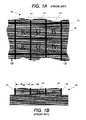
- Fig. 1A is a plan view of a color filter for a flat panel display according to the prior art.
- Fig. 1B is a profile view of the color filter for Fig. 1 A.
- Fig. 2A is a cross sectional view of a structure at a first stage in the process of forming a sub-pixel frame according to one embodiment of the present invention.
- Fig. 2B is a plan view of the structure shown in Fig. 2A.
- Fig. 2C is a cross sectional view of a structure at a second stage in the process of forming a sub-pixel frame according to one embodiment of the present invention.
- Fig. 2D is a plan view of the structure shown in Fig. 2C.
- Fig. 2E is a cross sectional view of a structure at a third stage in the process of forming a sub-pixel frame according to one embodiment of the present invention.
- Fig. 2F is a plan view of the structure shown in Fig. 2E.
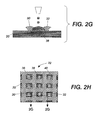
- Fig. 2G is a cross sectional view of a structure at a fourth stage in the process of forming a sub-pixel frame according to one embodiment of the present invention.
- Fig. 2H is a plan view of the structure shown in Fig. 2G.
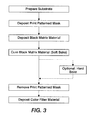
- Fig. 3 is a process flow diagram illustrating the steps involved in the formation of a sub-pixel frame according to one embodiment of the present invention.
- Fig. 4A is a cross sectional view of a structure at a first stage in the process of forming a sub-pixel frame according to a second embodiment of the present invention.
- Fig. 4B is a plan view of the structure shown in Fig. 4A.
- Fig. 4C is a cross sectional view of a structure at a second stage in the process of forming a sub-pixel frame according to the second embodiment of the present invention.
- Fig. 4D is a plan view of the structure shown in Fig. 4C.
- Fig. 4E is a cross sectional view of a structure at a third stage in the process of forming a sub-pixel frame according to the second embodiment of the present invention.
- Fig. 4F is a plan view of the structure shown in Fig. 4E.
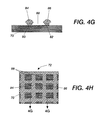
- Fig. 4G is a cross sectional view of a structure at a fourth stage in the process of forming a sub-pixel frame according to the second embodiment of the present invention.
- Fig. 4H is a plan view of the structure shown in Fig. 4G.
- Fig. 41 is a cross sectional view of a structure at a fifth stage in the process of forming a sub-pixel frame according to the second embodiment of the present invention.
- Fig. 4J is a plan view of the structure shown in Fig. 41.
- Fig. 5 is a process flow diagram illustrating the steps involved in the formation of a sub-pixel frame according to one embodiment of the present invention.
- With reference initially to Figs. 1A and 1B, there is shown therein a structure of the type formed by one embodiment of the present invention. Figs. 1A and 1 B are illustrations of a portion of a
color filter 10 for a plat-panel display. As mentioned, such a filter comprises a number ofpixels 12, each pixel being composed of three or more sub-pixels 14. The actual geometry of the sub-pixels, such as triangular, striped, diagonal, etc. is not critical to the operation of the present invention, but will be discussed in further detail below. Sub-pixels 14 are each primarily transparent to a specific color of light, such as red, green or blue. The individual sub-pixels 14 are separated by apixel frame 16.Pixel frame 16 is composed of a number of horizontal and vertical elements which form cavities, shown in Fig. 1 B, for the receipt ofmaterial forming sub-pixels 14. For reference, it will be assumed that the width wsp of each sub-pixel is on the order of 25 to 30 µm and the width Wf of each pixel frame element is on the order of 10 µm. - In order to form the structure illustrated in Figs. 1A and 1B, specific steps according to the present invention are described. Figs. 2A through 2H illustrate the structure at several intermediate stages of its production according to a process illustrated in Fig. 3. While the following description makes specific reference to the structure illustrated in Figs. 2A through 2H, without making more specific reference thereto the description is following the sequence illustrated in Fig. 3.
- With reference initially to Fig. 2A, the process begins with a
suitable substrate 20, such as glass or plastic, such as poly ethylene napthalate, onto which mask 22 is formed.Mask 22 is preferably formed by a digital lithographic process (and hence referred to as a "print patterned mask"), and comprises individual or coalesced droplets of a phase change material such as stearyl erucamide wax (for example, Kemamide 180-based wax from Crompton Corporation of Middlebury, Conn.), or similar material which is well controlled in terms of print quality (i.e., droplet size and shape, solidification time, hardness of solidified structure, etc.) Examples of systems appropriate for the ejection of droplets of phase change material include: ink-jet systems (such as disclosed inU.S. Patent 4,131,899 , which is incorporated herein by reference), ballistic aerosol marking (BAM) devices (such as disclosed inU.S. Patent 6,116,718 , which is incorporated herein by reference), acoustic ink printer (AIP) systems (U.S. Patent 4,959,674 , which is incorporated herein by reference), carrier-jet ejectors (as disclosed inU.S. patent 5,958,122 , which is incorporated by reference herein), deflection-controlled ink-jet systems (such as disclosed inU.S. Patent 3,958,252 , which is incorporated herein by reference), etc. Such systems also include pattern transfer systems, such as: xerographic, ionographic, screen, contact, and gravure printing systems, etc. - While the embodiment discussed herein involves the formation of a print patterned mask directly on
substrate 20, it is within the spirit and scope of the present invention that such a mask, and the features formed thereby, be formed over other layers, such as layers containing previously formed devices. Accordingly, it may be necessary to positionally register the formation ofmask 22. Registration is routinely accomplished in digital lithographic systems by use of fiduciary marks, digital imaging and processing, and processor controlled relative motion of the ejector and the substrate. The ability to align the mask layer through image processing prior to patterning is a significant advantage of the digital-lithographic process over other patterning methods. - For illustrative purposes, Fig. 2A shows three individual, adjacent but not contiguous digital lithographic masking elements (i.e., droplets) 24, 26, 28. A plan view of this arrangement is illustrated in Fig. 2B. For the purposes of illustration,
droplets - In select instances, adhesion promoters of the type commonly used with photoresist materials in the semiconductor processing art provide improved adhesion of the phase change material. For example, hexamethyldisilizane (HMDS) is used for chemically drying the substrate to promote adhesion. Other methods are annealing and plasma cleaning followed by an HMDS coating in order to clean and prepare the surface for photoresist adhesion.
- Considering that the elements of the sub-pixel frame (Figs. 1A, 1 B) are assumed to be on the order of 10 µm wide, and the digital lithographic masking elements (i.e., the individual droplets) are typically much wider (e.g., on the order of 25-30 µm), the digital lithographic masking elements do not make feasible feature masks. Accordingly, the masking elements are not used to directly mask such features, but are instead used as indirect masks.
- According to this embodiment, a black matrix material is deposited over selected portions of
mask 22, filling the interstices between the digitallithographic masking elements black matrix regions mask 22, and more precisely the digitallithographic masking elements - The black matrix material can be deposited using a number of techniques. If the mask material completely covers each pixel opening then the black matrix material can be coated onto the substrate by dip coating or by blade, or slit, coating. An alternative method is to fill the interstices by capillary filling as the masking elements may in certain embodiments form a set of open fluidic channels on the substrate. In this case, an appropriate volume of the liquid black matrix material can be deposited onto a small portion or portions of the substrate and maintained in liquid form in order to allow it to flow into the open channels across a larger portion of the substrate. This method can minimize printing of the black matrix, since the capillary or wicking forces provide an even distribution of the black matrix fluid over the array.
- According to one embodiment, the black matrix material is then cured by raising its temperature. To accomplish this, the structure may be placed in an oven at a desired temperature for a selected length of time. The temperature needed to cure the black matrix material must be lower than the melting temperature of the phase change material forming the digital
lithographic masking elements mask 22 must remain in place until the black matrix material is fully cured. Accordingly, the melting temperature of the phase change material must not be so high as to make it's ejection from the digital photolithographic system problematic, nor so low as to interfere with the curing of the black matrix material. An example of the conditions for an appropriate bake of the black matrix material are 50°C to 60°C for 15 to 20 minutes (but will ultimately depend on the actual selection of the black matrix material). - According to an alternate embodiment, the black matrix material may be another phase-change material that has a higher melting point than the mask material and can be selectively removed. For example, Corsair Wax (Xerox Corporation, Stamford, CT) has a high melting temperature and does not dissolve as readily in solvent as the aforementioned Kemamide wax. Thus, when tinted, the Corsair Wax may serve as a black matrix material. Furthermore, hardenable colloidal solutions (i.e., those that harden as the carrier solvent evaporates and leave behind the solid material such as nano-particles) can be processed as a liquid and dry as a solid. Thus, an appropriate colloidal solution bearing tinted solids may be deposited to form the black matrix. In each case, however, curing is replaced with a corresponding process (i.e., cooling, evaporation) for producing a hardened black matrix.
- According to a still further alternate embodiment, the black matrix material is a thermally curable polymer with suspended dark pigment. The processing of the black matrix material in this case involves careful control of the degree of curing, or cross-linking, in the black matrix film. After deposition of the black matrix material, the film is partially cured to a point to permit patterning by development in standard TMAH baths. These types of black matrix materials are commercially available, such as DARC 400 from Brewer Science (Danvers, MA).
- Once the black matrix material is hardened, and self-supporting
black matrix regions mask 22 may be removed. One of a variety of solvents may be used for this purpose, such as SVC-28 (MicroChem Corporation, Newton, MA). SVC-28 is a debonding solution manufactured by Rohm-Hass. The active ingredients are dipropylene glycol monomethyl ether, citrus distallate, synthetic isoparraffinic hydrocarbon, and aliphatic hydrocarbon. Where the black matrix material is a polyimide-based material that is dissolved or suspended in organic solvents similar to positive photoresist material, a negative photoresist stripper may selectively remove the masking elements while leaving the cured black matrix material unaffected. (Thus, the solvent used will depend upon the actual selection of the materials forming the digital lithographic masking elements and the black matrix regions.) The solvent selectively removes the masking material but not the cured black matrix material nor the substrate (or any devices or layers on which the aforementioned structure is formed). This is illustrated in cross-section in Fig. 2E and in plan view in Fig. 2F. - In certain circumstances, it may be desirable to form attack points for the removal of the digital lithographic masking elements. These are points where the solvent is provided greater access to the surface of the masking elements. Once the black matrix material is cured by the relatively low temperature bake (referred to as a "soft bake"), the structure may be subjected to a second, higher temperature bake, on the order of 120°C to 150°C for 5 to 15 minutes (referred to as a "hard bake"). The hard bake causes a partial melting of the masking elements, and a consequent disconnection of the masking material from the surface of the cured black matrix material. The gap thus formed between the black matrix material and the masking material allows the solvent better access to the masking material, and hence a more thorough and complete removal of that material from the structure. However, the hard bake is an optional step in the process.
- After removal of the mask, some formulations of the black matrix will need a further curing step to fully harden the material. Typical temperatures for such steps are 150 C or higher.
- At this point the structure comprises robust
black matrix structures structures structures black matrix structures - The removal of the masking material results in the formation of
wells 34 in the regions between the self-supporting blackmatrix material regions 2E. Wells 34 are bounded on all sides by the black matrix material, as illustrated in Fig. 2F. Thus,wells 34 form convenient receptacles for color filter material. The color filter material may comprise a pigmented polymer, for example. The pigment may selectively permit the transmission of red, green or blue light. The appropriate color filter material may thus be deposited, for example by a digital lithographic system, into selected wells to form sub-pixels for the color filter, as shown in Fig. 2G. For example, an ink jet printing system may be employed to first fill every first, fourth, seventh, etc., well with a red tinted filter material. That same system may then be employed to deposit a green tinted filter material in every second, fifth, eighth, etc., well. And likewise, a blue tinted color filter material may be deposited in a third pass over the structure into every third, sixth, ninth, etc., well. The color filter material is typically thermally cured to harden the film. The color filter with filledwells - In the deposition of the color filter materials, care must be taken to prevent cross-contamination of the various individual color filter materials. For example, any introduction of the green color filter material into the well containing the red color filter material will result in poor color separation of the final display. Such cross contamination can occur due to inaccuracies in the filling of the wells, from physical disruption of the color filter structure, from inadequate sub-pixel frame structure, and from wetting of the color filter material causing it to spread out of its designated well and into surrounding wells. One advantage of the present invention is that the cross sections of the sub-pixel frame elements (the black matrix features) will tend to be concave or curve inward toward the top of the well. This stands in sharp contrast to prior art structures, which typically have a profile tapering outward toward the top of the well, which in fact promotes wetting of the color filter material into neighboring wells. It will be appreciated that the degree of curvature or concavity of the sub-pixel frame elements may be controlled by controlling the degree of spreading of the print patterned masking elements.
- Furthermore, according to another embodiment of the preset invention, the black matrix material may be "engineered" to have desired hydrophobic or hydrophilic properties along its elevation to assist in preventing such wetting-induced cross-contamination. The black matrix material may be formed as a multiple layered structure with lower layers more hydrophilic and upper layers more hydrophobic. The black matrix material may be deposited in layers, with intermediate curing or hardening to avoid intermixture of the layers, or may be deposited as a single compound, then treated, for example by thermal annealing, to separate the materials into distinct layers. Such a structure advantageously reduces the tendency of the color filter material to wet across sub-pixel frame boundaries.
- A structure produced by a process according to this aspect of the present invention is shown in Figs. 4A through 4J. Fig. 5 illustrates the process flow according to this embodiment. Initially, the structure is quite similar to that described above with regard to Figs. 2A and 2B. With reference to Fig. 4A, a
suitable substrate 70 is selected, such as glass, silicon, fused silica, quartz, MgO, sapphire, glass or plastic, such as poly ethylene napthalate. In the case in which a color filter panel is to be produced, the substrate will typically be a transparent material, such as glass or plastic. Print patternedmask 72 is formed onsubstrate 70. Print patternedmask 72 is preferably formed by a digital lithographic process, and comprises a number of spaced-apart mask features 74, 76, 78. Adhesion promoters may be employed and alignment may be accomplished as previously discussed. Fig. 4B is a plan view of the structure at this point in its fabrication. - With reference now to Fig. 4C, a first black matrix material is deposited over selected portions of
mask 72, partially filling the interstices between the maskingelements black matrix regions elements - With reference now to Fig. 4E, a second black matrix material is deposited over first
black matrix regions elements black matrix regions - In the case of using a bilayer structure to form the structure for the black matrix, one of the layer could have a different transparency than the other. This structure is useful for cases where it may be difficult to achieve the appropriate difference in wetability if both layers are pigmented to the same extent. For example, the hydrophobic upper layer could be transparent if the optical density of the lower hydrophilic layer is high enough.
- At this point,
mask 72 may be removed, with or without the optional hard bake to create supplemental attack points. The solvent used for removingmask 72 will depend upon the actual selection of the material forming the digital lithographic masking elements, but may include the aforementioned tetrahydrofuran or heated SVC-28. (In the case that mask 72 is a wax, at a temperature above the melting point of the wax, SVC-28 will remove the wax from the surface even though SVC-28 is a surfactant in which the wax does not readily dissolve.) The solvent selectively removes the masking material but not the first or second cured black matrix materials nor the substrate (or any devices or layers on which the aforementioned structure is formed). This is illustrated in cross-section in Fig. 4G and in plan view in Fig. 4H. - Although the material forming the lower and upper portions of the remaining black matrix structures are different, the conditions for the curing of the layers allows the layers to structurally bond, forming structurally robust, free-standing bi-layer black
matrix material structures 80/84, 82/86 in which the lower regions are hydrophilic and the upper regions are hydrophobic. These structures definewells 88, as shown in Fig.4G. Wells 88 are then filled with color filter material, as previously discussed and shown in Fig. 41. The color filter with filledwells - Generally,
multilayed structures 80/84, 82/86 may by engineered for a variety of desirable attributes, and capability not readily available from processes known in the art. For example, in the case where such structures serve as micromechanical actuators, they may be provided with a more flexible material at their base and a less flexible material at their tips. In the case where such structures are bioelectrical devices, they may be provided with greater reactivity to a material at the base thereof and a lesser reactivity to a material at the tip thereof, and so on. - While a plurality of preferred exemplary embodiments have been presented in the foregoing detailed description, it should be understood that a vast number of variations exist, and these preferred exemplary embodiments are merely representative examples, and are not intended to limit the scope, applicability or configuration of the invention in any way. For example, while the process of the present invention has been described to form a sub-pixel frame, the process may be used to form a wide variety of other structures, such as exposure or etch masks, contacts or elements of microelectronic, optoelectronic, bioelectronic, etc., devices, and other physical structures. Furthermore, while references to matrix material herein have been to a "black" matrix material, the actual color of the material is not critical, and the degree of opacity of the material in its final state is a function of the design targets of the device being fabricated.
Claims (10)
- A method of forming a structure over a substrate, comprising the steps of:depositing a phase change material over the substrate;
the phase change material deposited using a printing system comprising a printhead;
the printhead including at least one ejector for ejecting the phase change material in liquid phase;
the phase change material deposited in a first printed pattern such that the first printed pattern remains following a change from liquid phase to solid phase of the phase change material;
the first printed pattern defining gaps;depositing a target material at least partially into the gaps to form target material features; andremoving the phase change material, leaving the target features on the substrate. - The method of claim 1, wherein the target material is deposited using a printing system comprising a printhead which includes at least one ejector for ejecting the target material in liquid phase, and the target material is deposited so as to form a second pattern such that the target material is primarily introduced into the gaps defined by the first printed pattern.
- The method of claim 1, further comprising the step of hardening the target material by heating the target material.
- The method of claim 3 wherein the temperature to which the target material is heated is below the melting temperature of the phase change material.
- The method of claim 4, wherein following the step of hardening the target material, the target material and phase change material are heated to a temperature exceeding the melting temperature of the phase change material.
- The method of claim 1, wherein the step of removing the phase change material comprises applying a solvent which removes the phase change material but does not affect the target material.
- A method of forming a sub-pixel frame for a color filter, comprising the steps of:depositing a phase change material over a substrate;
the phase change material deposited using a printing system comprising a printhead;
the printhead including at least one ejector for ejecting the phase change material in liquid phase;
the phase change material deposited in a first printed pattern such that the first printed pattern remains following a change from liquid phase to solid phase of the phase change material;
the first printed pattern defining gaps;depositing a black matrix material;
the black matrix material deposited using a printing system comprising a printhead;
the printhead including at least one ejector for ejecting the black matrix material in liquid phase;
the black matrix material deposited in a second printed pattern such that the black matrix material is selectively introduced into the gaps defined by the first printed pattern;heating the black matrix material such that the black matrix material hardens to form black matrix material features; andremoving the phase change material, leaving the black matrix features on the substrate. - The method of claim 7, further comprising the step of introducing a hardenable pigmented fluid into interstitial regions between the black matrix features.
- A method of forming a color filter comprising the steps of:depositing a phase change material onto a substrate;
the phase change material deposited using a printing system comprising a printhead;
the printhead including at least one ejector for ejecting the phase change material in liquid phase;
the phase change material deposited in a first printed pattern such that the first printed pattern remains following a change from liquid phase to solid phase of the phase change material;
the first printed pattern defining gaps;depositing a black matrix material;
the black matrix material deposited using a printing system comprising a printhead;
the printhead including at least one ejector for ejecting the black matrix material in liquid phase;
the black matrix material deposited in a second printed pattern such that the black matrix material is selectively introduced into the gaps defined by the first printed pattern;heating the black matrix material to a temperature below the melting point of the phase change material, such that the black matrix material hardens to form black matrix material features;heating the black matrix material and phase change material to a temperature above the melting temperature of the phase change material;removing the phase change material using a solvent which dissolves the phase change material but leaves the black matrix features unaffected on the substrate;depositing a hardenable pigmented fluid, using a printing system comprising a printhead which includes at least one ejector for ejecting the hardenable pigmented fluid in liquid phase, onto the substrate in a third pattern, such that the hardenable pigmented fluid is deposited into interstitial regions between the black matrix features; andhardening the hardenable pigmented fluid. - The method of claim 9, wherein the black matrix material features form a plurality of structures being enclosed on all lateral sides thereby, and further where the substrate forms a base of the structures, such that the structures may receive and substantially contain a material deposited therein, and still further wherein the step of depositing a hardenable pigmented fluid comprises the steps of:depositing in a first group of said structures a hardenable pigmented fluid primarily transmissive to a first wavelength range;depositing in a second group of said structures a hardenable pigmented fluid primarily transmissive to a second wavelength range different than said first wavelength range; anddepositing in a third group of said structures a hardenable pigmented fluid primarily transmissive to a third wavelength range different than said first and second wavelength ranges.
Applications Claiming Priority (1)
| Application Number | Priority Date | Filing Date | Title |
|---|---|---|---|
| US10/536,102 US7365022B2 (en) | 2006-01-20 | 2006-01-20 | Additive printed mask process and structures produced thereby |
Publications (2)
| Publication Number | Publication Date |
|---|---|
| EP1811331A2 true EP1811331A2 (en) | 2007-07-25 |
| EP1811331A3 EP1811331A3 (en) | 2008-04-23 |
Family
ID=37964496
Family Applications (1)
| Application Number | Title | Priority Date | Filing Date |
|---|---|---|---|
| EP07100905A Ceased EP1811331A3 (en) | 2006-01-20 | 2007-01-22 | Additive printed mask process and structures produced thereby |
Country Status (3)
| Country | Link |
|---|---|
| US (2) | US7365022B2 (en) |
| EP (1) | EP1811331A3 (en) |
| JP (1) | JP5074048B2 (en) |
Cited By (2)
| Publication number | Priority date | Publication date | Assignee | Title |
|---|---|---|---|---|
| ES2467641A1 (en) * | 2014-03-27 | 2014-06-12 | Thick Imaging, S. L. U. | Mask for printing and digital operation, and procedures of operation and printing on a substrate from this mask (Machine-translation by Google Translate, not legally binding) |
| US9093475B2 (en) | 2012-03-28 | 2015-07-28 | Sharp Laboratories Of America, Inc | Thin film transistor short channel patterning by substrate surface energy manipulation |
Families Citing this family (26)
| Publication number | Priority date | Publication date | Assignee | Title |
|---|---|---|---|---|
| US7378738B2 (en) * | 2003-09-02 | 2008-05-27 | International Business Machines Corporation | Method for producing self-aligned mask, articles produced by same and composition for same |
| KR101281877B1 (en) * | 2006-09-18 | 2013-07-03 | 엘지디스플레이 주식회사 | Color filter array panel and Fabricating method thereof |
| US8821799B2 (en) | 2007-01-26 | 2014-09-02 | Palo Alto Research Center Incorporated | Method and system implementing spatially modulated excitation or emission for particle characterization with enhanced sensitivity |
| US9164037B2 (en) | 2007-01-26 | 2015-10-20 | Palo Alto Research Center Incorporated | Method and system for evaluation of signals received from spatially modulated excitation and emission to accurately determine particle positions and distances |
| EP2188059B1 (en) * | 2007-08-24 | 2016-05-04 | Advanced Liquid Logic, Inc. | Bead manipulations on a droplet actuator |
| EP2085797B1 (en) | 2008-01-30 | 2016-06-01 | Palo Alto Research Center Incorporated | Producing Filters with Combined Transmission and/or Reflection Functions |
| US7894068B2 (en) * | 2008-02-04 | 2011-02-22 | Palo Alto Research Center Incorporated | Producing filters with combined transmission and/or reflection functions |
| US7701580B2 (en) * | 2008-02-01 | 2010-04-20 | Palo Alto Research Center Incorporated | Transmitting/reflecting emanating light with time variation |
| EP2085761B1 (en) | 2008-01-30 | 2018-11-28 | Palo Alto Research Center Incorporated | Obtaining sensing results indicating time variation |
| US7817254B2 (en) | 2008-01-30 | 2010-10-19 | Palo Alto Research Center Incorporated | Obtaining information from time variation of sensing results |
| US8153949B2 (en) * | 2008-12-18 | 2012-04-10 | Palo Alto Research Center Incorporated | Obtaining sensing results indicating time variation |
| EP2085762B1 (en) | 2008-01-30 | 2018-07-04 | Palo Alto Research Center Incorporated | Transmitting/reflecting emanating light with time variation |
| US8629981B2 (en) | 2008-02-01 | 2014-01-14 | Palo Alto Research Center Incorporated | Analyzers with time variation based on color-coded spatial modulation |
| US8373860B2 (en) | 2008-02-01 | 2013-02-12 | Palo Alto Research Center Incorporated | Transmitting/reflecting emanating light with time variation |
| KR101058846B1 (en) * | 2008-12-31 | 2011-08-23 | 한국생산기술연구원 | Phase change memory manufacturing method using inkjet printing |
| DE102010013755A1 (en) | 2009-04-02 | 2010-10-14 | Optrex Europe Gmbh | Cascaded structures i.e. separators, manufacturing method for manufacturing organic LED displays, involves making surface region of substrate invulnerable, so that bar remains below invulnerable region |
| DE102009019761B4 (en) * | 2009-05-05 | 2017-08-24 | SECCO-Spezial-Elektronik und Computer-Cooperations-Gesellschaft mbH | Method for applying optical filter structures to a carrier substrate |
| US8211782B2 (en) * | 2009-10-23 | 2012-07-03 | Palo Alto Research Center Incorporated | Printed material constrained by well structures |
| US9029800B2 (en) | 2011-08-09 | 2015-05-12 | Palo Alto Research Center Incorporated | Compact analyzer with spatial modulation and multiple intensity modulated excitation sources |
| US8723140B2 (en) | 2011-08-09 | 2014-05-13 | Palo Alto Research Center Incorporated | Particle analyzer with spatial modulation and long lifetime bioprobes |
| US9791080B2 (en) | 2012-03-12 | 2017-10-17 | Idex Health & Science Llc | Microfluidic interconnect |
| US8796083B2 (en) | 2012-05-15 | 2014-08-05 | Sharp Laboratories Of America, Inc. | Fluoropolymer mask for transistor channel definition |
| CN104979372B (en) * | 2015-05-20 | 2018-03-02 | 京东方科技集团股份有限公司 | Display base plate and preparation method thereof and display device |
| KR20180064611A (en) * | 2016-12-05 | 2018-06-15 | 삼성디스플레이 주식회사 | Display device and manufacturing method thereof |
| CN111769141A (en) * | 2020-06-23 | 2020-10-13 | 武汉华星光电半导体显示技术有限公司 | Color filter, preparation method of color filter and display panel |
| CN113253510B (en) * | 2021-05-19 | 2022-11-04 | 惠科股份有限公司 | Color film substrate and manufacturing method thereof |
Citations (5)
| Publication number | Priority date | Publication date | Assignee | Title |
|---|---|---|---|---|
| US197754A (en) | 1877-12-04 | Improvement in looms | ||
| KR20000033721A (en) * | 1998-11-25 | 2000-06-15 | 구본준 | Method for producing color filter of liquid crystal display device |
| WO2001011426A1 (en) * | 1999-05-27 | 2001-02-15 | Patterning Technologies Limited | Method of forming a masking pattern on a surface |
| US6742884B2 (en) | 2001-04-19 | 2004-06-01 | Xerox Corporation | Apparatus for printing etch masks using phase-change materials |
| US6838361B2 (en) | 2001-03-09 | 2005-01-04 | Seiko Epson Corporation | Method of patterning a substrate |
Family Cites Families (25)
| Publication number | Priority date | Publication date | Assignee | Title |
|---|---|---|---|---|
| US3958252A (en) * | 1971-11-12 | 1976-05-18 | Casio Computer Co., Ltd. | Ink jet type character recording apparatus |
| US4131899A (en) * | 1977-02-22 | 1978-12-26 | Burroughs Corporation | Droplet generator for an ink jet printer |
| US4121899A (en) * | 1977-03-04 | 1978-10-24 | Milliken Research Corporation | Condensation dyeing |
| GB2127751B (en) | 1982-10-06 | 1986-04-23 | Plessey Co Plc | Producing narrow features in electrical devices |
| US4533624A (en) * | 1983-05-23 | 1985-08-06 | Sperry Corporation | Method of forming a low temperature multilayer photoresist lift-off pattern |
| JPS643663A (en) | 1987-06-26 | 1989-01-09 | Toshiba Corp | Forming method for fine pattern |
| US4959674A (en) * | 1989-10-03 | 1990-09-25 | Xerox Corporation | Acoustic ink printhead having reflection coating for improved ink drop ejection control |
| JP3735885B2 (en) * | 1995-04-27 | 2006-01-18 | ソニー株式会社 | Printer device |
| JPH1039126A (en) * | 1996-04-09 | 1998-02-13 | Mitsubishi Chem Corp | Production of color filter |
| JPH11160862A (en) * | 1997-11-25 | 1999-06-18 | Hitachi Chem Co Ltd | Photosensitive element |
| US6116718A (en) * | 1998-09-30 | 2000-09-12 | Xerox Corporation | Print head for use in a ballistic aerosol marking apparatus |
| US6306933B1 (en) * | 1999-03-30 | 2001-10-23 | Union Carbide Chemicals & Plastics Technology Corporation | Cellulose ether slurries |
| KR100661291B1 (en) * | 1999-06-14 | 2006-12-26 | 엘지.필립스 엘시디 주식회사 | A color filter and a method for fabricating the same |
| JP3491156B2 (en) * | 2001-01-22 | 2004-01-26 | セイコーエプソン株式会社 | Liquid crystal device, method of manufacturing the same, and electronic equipment |
| US6872320B2 (en) * | 2001-04-19 | 2005-03-29 | Xerox Corporation | Method for printing etch masks using phase-change materials |
| US6605519B2 (en) * | 2001-05-02 | 2003-08-12 | Unaxis Usa, Inc. | Method for thin film lift-off processes using lateral extended etching masks and device |
| GB2379083A (en) * | 2001-08-20 | 2003-02-26 | Seiko Epson Corp | Inkjet printing on a substrate using two immiscible liquids |
| JP4058969B2 (en) * | 2002-03-15 | 2008-03-12 | セイコーエプソン株式会社 | Film forming apparatus, head cleaning method, device manufacturing apparatus and device |
| US6972261B2 (en) * | 2002-06-27 | 2005-12-06 | Xerox Corporation | Method for fabricating fine features by jet-printing and surface treatment |
| US6890050B2 (en) * | 2002-08-20 | 2005-05-10 | Palo Alto Research Center Incorporated | Method for the printing of homogeneous electronic material with a multi-ejector print head |
| US6759713B2 (en) * | 2002-11-22 | 2004-07-06 | Xerox Corporation | Electronic device structures including interconnecting microfluidic channels |
| US6872588B2 (en) * | 2002-11-22 | 2005-03-29 | Palo Alto Research Center Inc. | Method of fabrication of electronic devices using microfluidic channels |
| JP3895269B2 (en) * | 2002-12-09 | 2007-03-22 | 富士通株式会社 | Resist pattern forming method, semiconductor device, and manufacturing method thereof |
| US7309563B2 (en) * | 2003-12-19 | 2007-12-18 | Palo Alto Research Center Incorporated | Patterning using wax printing and lift off |
| US7172842B2 (en) * | 2004-05-12 | 2007-02-06 | Chunghwa Picture Tubes, Ltd. | Color filter array plate and method of fabricating the same |
-
2006
- 2006-01-20 US US10/536,102 patent/US7365022B2/en not_active Expired - Fee Related
-
2007
- 2007-01-22 JP JP2007011715A patent/JP5074048B2/en not_active Expired - Fee Related
- 2007-01-22 EP EP07100905A patent/EP1811331A3/en not_active Ceased
-
2008
- 2008-03-11 US US12/046,242 patent/US7749916B2/en not_active Expired - Fee Related
Patent Citations (5)
| Publication number | Priority date | Publication date | Assignee | Title |
|---|---|---|---|---|
| US197754A (en) | 1877-12-04 | Improvement in looms | ||
| KR20000033721A (en) * | 1998-11-25 | 2000-06-15 | 구본준 | Method for producing color filter of liquid crystal display device |
| WO2001011426A1 (en) * | 1999-05-27 | 2001-02-15 | Patterning Technologies Limited | Method of forming a masking pattern on a surface |
| US6838361B2 (en) | 2001-03-09 | 2005-01-04 | Seiko Epson Corporation | Method of patterning a substrate |
| US6742884B2 (en) | 2001-04-19 | 2004-06-01 | Xerox Corporation | Apparatus for printing etch masks using phase-change materials |
Cited By (3)
| Publication number | Priority date | Publication date | Assignee | Title |
|---|---|---|---|---|
| US9093475B2 (en) | 2012-03-28 | 2015-07-28 | Sharp Laboratories Of America, Inc | Thin film transistor short channel patterning by substrate surface energy manipulation |
| ES2467641A1 (en) * | 2014-03-27 | 2014-06-12 | Thick Imaging, S. L. U. | Mask for printing and digital operation, and procedures of operation and printing on a substrate from this mask (Machine-translation by Google Translate, not legally binding) |
| WO2015144967A2 (en) | 2014-03-27 | 2015-10-01 | Thick Imaging, S.L.U. | Mask for digital operation and printing, and methods for operation and printing on a substrate using said mask |
Also Published As
| Publication number | Publication date |
|---|---|
| US20080153014A1 (en) | 2008-06-26 |
| JP2007193344A (en) | 2007-08-02 |
| US7365022B2 (en) | 2008-04-29 |
| EP1811331A3 (en) | 2008-04-23 |
| US20070172969A1 (en) | 2007-07-26 |
| JP5074048B2 (en) | 2012-11-14 |
| US7749916B2 (en) | 2010-07-06 |
Similar Documents
| Publication | Publication Date | Title |
|---|---|---|
| US7365022B2 (en) | Additive printed mask process and structures produced thereby | |
| EP1906229B1 (en) | Process for forming a feature by undercutting a printed mask | |
| DE60119311T2 (en) | PROCESS FOR PRODUCING A COLOR ELECTROOPTIC DEVICE | |
| JP4291411B2 (en) | Apparatus and method for printing color filters | |
| US7384568B2 (en) | Method of forming a darkfield etch mask | |
| US20070165057A1 (en) | Substrate structure and method for forming patterned layer on the same | |
| US8736991B2 (en) | Color filter array and manufacturing method thereof | |
| KR101074077B1 (en) | Light-shielding layer for display device and forming method thereof | |
| JP2005063785A (en) | Barrier pattern and its forming method | |
| CN108428808B (en) | The production method of organic electroluminescent substrate | |
| CN104907227B (en) | Method for forming film and apparatus for forming the same | |
| US8663783B2 (en) | Thin-film layer structure and method for manufacturing same | |
| TWI484301B (en) | A method of forming a continuous three-dimentional structure by inkjet printing process | |
| CN101231361A (en) | Method for manufacturing substrate with thin membrane pattern layer | |
| JP2003043243A (en) | Color filter for display device | |
| JP4480517B2 (en) | Thin film pattern forming substrate, thin film pattern forming substrate manufacturing method, and thin film pattern forming substrate | |
| JP2019132890A (en) | Patterned substrate, partition wall formation method, method for manufacturing patterned substrate, partition wall formation device, and device for manufacturing patterned substrate | |
| US20110146905A1 (en) | Method for forming patterned layer on substrate structure | |
| JP2003139935A (en) | Multicolor pixel composition for flat panel display device | |
| JP2004301928A (en) | Thin film deposition method and body to be processed having thin film | |
| JP2005081726A (en) | Pattern printing equipment using intaglio of flexible metal flat sheet | |
| JP2005507566A (en) | Method for forming a mask on a surface | |
| KR100881492B1 (en) | Patterned thinfilm layer and method for manufacturing same | |
| JP2015060027A (en) | Coating liquid solidification method and coating liquid solidification device | |
| CN1797201B (en) | Method for fabricating micro image |
Legal Events
| Date | Code | Title | Description |
|---|---|---|---|
| PUAI | Public reference made under article 153(3) epc to a published international application that has entered the european phase |
Free format text: ORIGINAL CODE: 0009012 |
|
| AK | Designated contracting states |
Kind code of ref document: A2 Designated state(s): AT BE BG CH CY CZ DE DK EE ES FI FR GB GR HU IE IS IT LI LT LU LV MC NL PL PT RO SE SI SK TR |
|
| AX | Request for extension of the european patent |
Extension state: AL BA HR MK YU |
|
| PUAL | Search report despatched |
Free format text: ORIGINAL CODE: 0009013 |
|
| AK | Designated contracting states |
Kind code of ref document: A3 Designated state(s): AT BE BG CH CY CZ DE DK EE ES FI FR GB GR HU IE IS IT LI LT LU LV MC NL PL PT RO SE SI SK TR |
|
| AX | Request for extension of the european patent |
Extension state: AL BA HR MK RS |
|
| RIC1 | Information provided on ipc code assigned before grant |
Ipc: G02F 1/1335 20060101ALI20080319BHEP Ipc: G03F 7/00 20060101AFI20080319BHEP |
|
| 17P | Request for examination filed |
Effective date: 20081023 |
|
| AKX | Designation fees paid |
Designated state(s): DE FR GB |
|
| 17Q | First examination report despatched |
Effective date: 20081223 |
|
| STAA | Information on the status of an ep patent application or granted ep patent |
Free format text: STATUS: THE APPLICATION HAS BEEN REFUSED |
|
| 18R | Application refused |
Effective date: 20130315 |