EP1744448B1 - Radio frequency amplifiers - Google Patents
Radio frequency amplifiers Download PDFInfo
- Publication number
- EP1744448B1 EP1744448B1 EP06015328A EP06015328A EP1744448B1 EP 1744448 B1 EP1744448 B1 EP 1744448B1 EP 06015328 A EP06015328 A EP 06015328A EP 06015328 A EP06015328 A EP 06015328A EP 1744448 B1 EP1744448 B1 EP 1744448B1
- Authority
- EP
- European Patent Office
- Prior art keywords
- transistor
- input
- signal
- control
- output
- Prior art date
- Legal status (The legal status is an assumption and is not a legal conclusion. Google has not performed a legal analysis and makes no representation as to the accuracy of the status listed.)
- Expired - Lifetime
Links
- 230000003019 stabilising effect Effects 0.000 claims description 9
- 230000000694 effects Effects 0.000 claims description 8
- 230000008878 coupling Effects 0.000 claims description 5
- 238000010168 coupling process Methods 0.000 claims description 5
- 238000005859 coupling reaction Methods 0.000 claims description 5
- 238000000034 method Methods 0.000 claims description 4
- 230000001105 regulatory effect Effects 0.000 description 4
- 239000004065 semiconductor Substances 0.000 description 4
- 230000008901 benefit Effects 0.000 description 2
- 230000001413 cellular effect Effects 0.000 description 2
- 230000003247 decreasing effect Effects 0.000 description 2
- 238000010438 heat treatment Methods 0.000 description 2
- 230000008859 change Effects 0.000 description 1
- 238000005094 computer simulation Methods 0.000 description 1
- 230000001276 controlling effect Effects 0.000 description 1
- 238000010586 diagram Methods 0.000 description 1
- 230000005669 field effect Effects 0.000 description 1
- 230000006872 improvement Effects 0.000 description 1
- 238000004519 manufacturing process Methods 0.000 description 1
- 239000002184 metal Substances 0.000 description 1
- 229910044991 metal oxide Inorganic materials 0.000 description 1
- 150000004706 metal oxides Chemical class 0.000 description 1
- 230000004048 modification Effects 0.000 description 1
- 238000012986 modification Methods 0.000 description 1
- 230000003071 parasitic effect Effects 0.000 description 1
- 230000006641 stabilisation Effects 0.000 description 1
Images

Classifications
-
- H—ELECTRICITY
- H03—ELECTRONIC CIRCUITRY
- H03F—AMPLIFIERS
- H03F3/00—Amplifiers with only discharge tubes or only semiconductor devices as amplifying elements
- H03F3/189—High-frequency amplifiers, e.g. radio frequency amplifiers
- H03F3/19—High-frequency amplifiers, e.g. radio frequency amplifiers with semiconductor devices only
-
- H—ELECTRICITY
- H03—ELECTRONIC CIRCUITRY
- H03F—AMPLIFIERS
- H03F1/00—Details of amplifiers with only discharge tubes, only semiconductor devices or only unspecified devices as amplifying elements
- H03F1/30—Modifications of amplifiers to reduce influence of variations of temperature or supply voltage or other physical parameters
- H03F1/302—Modifications of amplifiers to reduce influence of variations of temperature or supply voltage or other physical parameters in bipolar transistor amplifiers
-
- H—ELECTRICITY
- H03—ELECTRONIC CIRCUITRY
- H03F—AMPLIFIERS
- H03F2200/00—Indexing scheme relating to amplifiers
- H03F2200/366—Multiple MOSFETs are coupled in parallel
-
- H—ELECTRICITY
- H03—ELECTRONIC CIRCUITRY
- H03F—AMPLIFIERS
- H03F2200/00—Indexing scheme relating to amplifiers
- H03F2200/504—Indexing scheme relating to amplifiers the supply voltage or current being continuously controlled by a controlling signal, e.g. the controlling signal of a transistor implemented as variable resistor in a supply path for, an IC-block showed amplifier
-
- H—ELECTRICITY
- H03—ELECTRONIC CIRCUITRY
- H03F—AMPLIFIERS
- H03F2203/00—Indexing scheme relating to amplifiers with only discharge tubes or only semiconductor devices as amplifying elements covered by H03F3/00
- H03F2203/20—Indexing scheme relating to power amplifiers, e.g. Class B amplifiers, Class C amplifiers
- H03F2203/21—Indexing scheme relating to power amplifiers, e.g. Class B amplifiers, Class C amplifiers with semiconductor devices only
- H03F2203/211—Indexing scheme relating to power amplifiers, e.g. Class B amplifiers, Class C amplifiers with semiconductor devices only using a combination of several amplifiers
- H03F2203/21131—Indexing scheme relating to power amplifiers, e.g. Class B amplifiers, Class C amplifiers with semiconductor devices only using a combination of several amplifiers the input bias voltage of a power amplifier being controlled, e.g. by a potentiometer or an emitter follower
Definitions
- the present invention relates to radio frequency amplifiers having a power transistor.
- the invention relates to providing temperature compensation for the power transistor of a radio frequency amplifier.
- Power transistors are commonly used in many radio frequency (RF) devices and circuits including those incorporated into cellular radio telephones and cellular radio base station transceivers. Often, the stability of the output power is critical to the correct operation of the device or circuit, not only to ensure accurate RF output power levels but also to prevent damage to transistor itself. A common cause of output power instability is variation of the operating temperature of the power transistor, such as can arise due to self-heating and changes in the ambient temperature.
- FIG. 1 A simple biasing arrangement is shown in Figure 1 , where an RF signal RF_IN to be amplified is coupled to the input of a power transistor Q1.
- the amplified RF signal RF_OUT is obtained from the collector of the power transistor.
- a driver transistor Q2 is also coupled to the input of the power transistor Q1 to bias the power transistor at a suitable operating point. Temperature changes will however tend to change the base-emitter voltages of both the power and driver transistor, changing the operating point and therefore gain of the power transistor Q1.
- the emitter resistance Re is large, an increase in gain and collector current will tend to be offset by a decrease in the base-emitter voltage introducing a degree of stability to the transistor.
- a large emitter resistance results in a large power loss across that resistance, decreasing the efficiency of the amplifier.
- FIG. 2 illustrates a modified power amplifier incorporating a typical temperature compensating biasing circuit.
- the circuit comprises a pair of diode-connected transistors Q3, Q4 connected between the base of the driver transistor Q2 and ground.
- the underlying operating theory is that the voltage drop across the two diode-connected transistors Q3, Q4 tracks that across the base-emitter junctions of the driver and power transistors Q1, Q2, maintaining the power transistor base current substantially constant and its operating point stable.
- additional stability is provided by the voltage drop across the emitter resistance Re although again this tends to reduce the efficiency of the amplifier.
- the temperature compensation circuit of Figure 2 is widely used, it is not ideal. Firstly, fluctuations in the bias voltage Vbias, usually generated from a regulated voltage (e.g. the supply voltage Vsup), have a significant effect on the collector current Ic of the power transistor Q1. Secondly, as the base-emitter regions of the two diode-connected transistors Q3, Q4 are not operating under exactly the same conditions as the power and driver transistors Q1, Q2 (for example they do not receive the RF input signal), the voltage drop across the former may not necessarily follow that across the base-emitter junctions of the latter, even if the operating temperatures of all four transistors are substantially identical. This problem is exacerbated by differences between the various transistors which arise from possibly wide manufacturing tolerances, even where the entire circuit is integrated onto a single semiconductor chip.
- Vbias usually generated from a regulated voltage (e.g. the supply voltage Vsup)
- Prior art publication EP 0 634 835 discloses an RF amplifier and a mixer, which comprise a bias circuit.
- power transistors Q1, Q2, ..., QN are connected in parallel.
- An RF signal is fed to these transistors.
- the amplified RF signal is achieved in output 22.
- the base of the control transistor Q is connected with the bases of the power transistors.
- the bias is fed to the power transistors from a differential amplifier through adjustable resistors.
- the differential amplifier has a negative feedback through the control transistor Q.
- the differential amplifier biases also the control transistor Q.
- a data sheet of an operational amplifier LM741 shows a solution for general purposes.
- the schematic diagram of LM741 reveals that the operational amplifier includes an output stage formed by transistors Q14, Q15 and Q20 with resistors R9 and R10.
- the transistor Q14 can be regarded as a driver transistor for Q15, and furthermore, the output of Q15 is also the output of the entire operational amplifier.
- a radio frequency amplifier comprising:
- Embodiments of the present invention provide a feedback signal from the output of the control transistor to the differential amplifier, which signal tends to drive the output of the differential amplifier, and therefore the power transistor control bias signal, to maintain the power amplifier at a substantially constant operating point.
- the present invention reduces the effect of temperature changes on the operating point of the power amplifier.
- the feedback loop provided by the control transistor and the differential amplifier further comprises low pass filter means arranged to remove the effect of radio frequency variations occurring at said output of the control transistor.
- the power transistor may have any suitable configuration. However, a preferred configuration consists of two or more transistor elements coupled in parallel.
- the power transistor and the control transistors are configured such that in the active state the current densities flowing through the transistors are substantially identical. More preferably, both the power and control transistors are provided with respective base and emitter resistances, where the values of the resistances are inversely proportional to the active area of the respective transistors.
- the differential amplifier of the present invention is an emitter coupled differential amplifier.
- Embodiments of the present invention may comprise a gain control signal coupled to said output of the control transistor and to said second input of the differential amplifier.
- the gain control signal may be used to vary the driver control signal applied to the driver transistor and therefore the control bias signal applied to the power transistor, thereby varying the operating point of the power transistor.
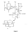
- Figure 3 illustrates an improved temperature compensation circuit for an RF amplifier comprising a power transistor Q1 and a driver transistor Q2.
- the driver transistor Q2 is provided by a single n-p-n bipolar junction transistor
- the power transistor is provided by a set (m in number where m may be, for example, 48) of n-p-n bipolar junction transistors (or transistor elements) with respective emitter and base resistances and RF input coupling capacitances, connected in parallel. This is illustrated in the inset A in Figure 3 .
- the temperature compensation circuit of Figure 3 comprises a control transistor Qc.
- the control transistor is provided by a single n-p-n bipolar junction transistor element substantially identical to one of the transistor elements making up the power transistor Q1.
- the active area of the control transistor Qc is 1/m times the effective active area of the power transistor Q1.
- the control transistor Qc is provided with a base resistance Rb and an emitter resistance Re whilst the power transistor Q1 is provided with a base resistance Rb/m and an emitter resistance of Re/m.
- the collector of the control transistor Qc is connected to a regulated dc voltage Vreg via a collector resistance R1.
- the collector of the control transistor Qc is also connected to the positive input of a differential amplifier.
- V1 is generated from the regulated voltage Vreg via a resistance divider network.
- the output voltage Vo of the differential amplifier is coupled via a stabilising resistance R2 to the base of the driver transistor Q2 which has its collector coupled to the supply voltage Vsup.
- the base of the driver transistor is also coupled to the base of the transistor Qd2 via a stabilising capacitance C1.
- the driver transistor Q2 is connected to the bases of the power and control transistors Q1, Qc via the respective base resistances to provide a biasing signal to both transistors.
- the base-emitter and collector-emitter current densities flowing through both transistors will be substantially the same. Changes in the collector current of the power transistor Q1, due for example to heating effects, can therefore be expected to be reflected in the collector current of the control transistor Qc, scaled down by a factor of m.
- the temperature of the power transistor Q1 rises after some period of operation, causing the collector current and therefore the RF gain of the transistor to increase, deviating from the desired operating point.
- the collector current of the control transistor Qc will increase proportionally, causing the transistor's collector voltage to decrease (due to the increase in the voltage drop across the collector resistance R1).
- the output voltage Vo of the differential amplifier will fall.
- the base current applied to the driver transistor Q2 then falls, decreasing the bias currents applied to the power and control transistors and reducing the gain of these transistors.
- the control transistor and the differential amplifier therefore have the effect of providing a negative feedback control signal to the driver transistor Q2 which tends to counteract changes in the properties of the power transistor Q1 which would otherwise cause the gain of the power transistor to fluctuate.
- the various passive components of the circuit are selected to ensure the correct operation of the circuit.
- the stabilising resistance R2 and C1 are selected and arranged to stabilise the performance of the feedback loop and in particular to remove the effects of high frequency variations occurring at the collector of the control transistor Qc whilst still enabling the circuit to respond quickly to output changes.
- Components can be selected using, for example, computer simulations.
- An important and surprising advantage of the circuit of Figure 3 is that the emitter resistance (Re/m) associated with the power transistor Q1 can be small relative to known circuits such as are illustrated in Figures 1 and 2 , indeed the resistance of bond wires connecting the emitters of the power transistor elements to ground, or even parasitic resistances, may be sufficient (to avoid current "hogging"). This is because a large temperature compensating emitter resistance is no longer required.
- the circuit of Figure 3 results in a reduced power loss across the emitter resistance and an improvement in the efficiency of the amplifier.
- Figure 3 also illustrates an optional gain control input in which a gain control voltage Vpc is applied to the collector of the control transistor Qc via a resistance R3.
- the voltage Vpc will tend to increase the input voltage V2 to the differential amplifier, in turn increasing the bias current provided by the driver transistor Q2. This will increase the RF gain of the power transistor Q1.
- the circuit of Figure 3 may be implemented with discrete components, but is preferably integrated into a single semiconductor chip. This has the advantage that the operating temperature of the various components, and in particular of the control and power transistors, will tend to be equalised.
- a preferred configuration involves arranging the transistor elements of the power transistor according to the "common centroid" geometry, and arranging the control transistor directly adjacent, or amongst, the transistor elements of the power transistor.
- the present invention may be applied to stabilise the properties of power field effect transistor (FET) such as a metal oxide semiconductor FET (MOSFET) or a metal semiconductor FET (MESFET), comprising a set of FET elements connected in parallel. Stabilisation is achieved using a gain control FET which forms part of a negative feedback loop.
- FET power field effect transistor
- MOSFET metal oxide semiconductor FET
- MESFET metal semiconductor FET
- gain control FET which forms part of a negative feedback loop.
- the configuration and arrangement of the control FET are such that the drain-source current density is substantially identical to that in the power FET.
Landscapes
- Engineering & Computer Science (AREA)
- Power Engineering (AREA)
- Amplifiers (AREA)
Description
- The present invention relates to radio frequency amplifiers having a power transistor. In particular, though not necessarily, the invention relates to providing temperature compensation for the power transistor of a radio frequency amplifier.
- Power transistors are commonly used in many radio frequency (RF) devices and circuits including those incorporated into cellular radio telephones and cellular radio base station transceivers. Often, the stability of the output power is critical to the correct operation of the device or circuit, not only to ensure accurate RF output power levels but also to prevent damage to transistor itself. A common cause of output power instability is variation of the operating temperature of the power transistor, such as can arise due to self-heating and changes in the ambient temperature.
- In order to ensure that a power transistor amplifies an RF signal with a desired gain, it is necessary to bias the transistor at a suitable "operating point". A simple biasing arrangement is shown in
Figure 1 , where an RF signal RF_IN to be amplified is coupled to the input of a power transistor Q1. The amplified RF signal RF_OUT is obtained from the collector of the power transistor. A driver transistor Q2 is also coupled to the input of the power transistor Q1 to bias the power transistor at a suitable operating point. Temperature changes will however tend to change the base-emitter voltages of both the power and driver transistor, changing the operating point and therefore gain of the power transistor Q1. Provided that the emitter resistance Re is large, an increase in gain and collector current will tend to be offset by a decrease in the base-emitter voltage introducing a degree of stability to the transistor. However, a large emitter resistance results in a large power loss across that resistance, decreasing the efficiency of the amplifier. -
Figure 2 illustrates a modified power amplifier incorporating a typical temperature compensating biasing circuit. The circuit comprises a pair of diode-connected transistors Q3, Q4 connected between the base of the driver transistor Q2 and ground. The underlying operating theory is that the voltage drop across the two diode-connected transistors Q3, Q4 tracks that across the base-emitter junctions of the driver and power transistors Q1, Q2, maintaining the power transistor base current substantially constant and its operating point stable. As with the circuit ofFigure 1 , additional stability is provided by the voltage drop across the emitter resistance Re although again this tends to reduce the efficiency of the amplifier. - Although the temperature compensation circuit of
Figure 2 is widely used, it is not ideal. Firstly, fluctuations in the bias voltage Vbias, usually generated from a regulated voltage (e.g. the supply voltage Vsup), have a significant effect on the collector current Ic of the power transistor Q1. Secondly, as the base-emitter regions of the two diode-connected transistors Q3, Q4 are not operating under exactly the same conditions as the power and driver transistors Q1, Q2 (for example they do not receive the RF input signal), the voltage drop across the former may not necessarily follow that across the base-emitter junctions of the latter, even if the operating temperatures of all four transistors are substantially identical. This problem is exacerbated by differences between the various transistors which arise from possibly wide manufacturing tolerances, even where the entire circuit is integrated onto a single semiconductor chip. - Prior art publication
EP 0 634 835 discloses an RF amplifier and a mixer, which comprise a bias circuit. In Figure 5 of the publication, power transistors Q1, Q2, ..., QN are connected in parallel. An RF signal is fed to these transistors. The amplified RF signal is achieved in output 22. The base of the control transistor Q is connected with the bases of the power transistors. The bias is fed to the power transistors from a differential amplifier through adjustable resistors. The differential amplifier has a negative feedback through the control transistor Q. Thus, the differential amplifier biases also the control transistor Q. - In prior art, there have been presented numerous operational amplifiers with their data sheets. As an example, a data sheet of an operational amplifier LM741 shows a solution for general purposes. The schematic diagram of LM741 reveals that the operational amplifier includes an output stage formed by transistors Q14, Q15 and Q20 with resistors R9 and R10. The transistor Q14 can be regarded as a driver transistor for Q15, and furthermore, the output of Q15 is also the output of the entire operational amplifier.
- It is an object of the present invention to provide a radio frequency amplifier which overcomes or at least mitigates the above noted disadvantages. This and other objects are achieved by providing an additional control transistor arranged to conduct a current density substantially identical to that conducted by the power transistor of the amplifier, and to provide a feedback signal for controlling biasing of the power transistor.
- According to a first aspect of the present invention there is provided a radio frequency amplifier comprising:
- a power transistor having an input for receiving a radio frequency signal to be amplified and an output for providing an amplified radio frequency signal;
- a control transistor having an input coupled to said input of the power transistor;
- a driver transistor having an output coupled to said inputs of the power and control transistors for providing a control bias signal to the power and control transistors; and
- a differential amplifier having a first input coupled to an input signal and an output coupled to an input of the driver transistor for providing a driver control signal to the driver transistor,
- the control transistor having an output coupled to a second input of the differential amplifier, wherein the output of the control transistor tends to follow the output of the power transistor and provides a negative feedback signal to the differential amplifier; and wherein
- a stabilising capacitance is provided between the input of the driver transistor and said second input of the differential amplifier.
- Embodiments of the present invention provide a feedback signal from the output of the control transistor to the differential amplifier, which signal tends to drive the output of the differential amplifier, and therefore the power transistor control bias signal, to maintain the power amplifier at a substantially constant operating point. The present invention reduces the effect of temperature changes on the operating point of the power amplifier.
- Preferably, the feedback loop provided by the control transistor and the differential amplifier further comprises low pass filter means arranged to remove the effect of radio frequency variations occurring at said output of the control transistor.
- The power transistor may have any suitable configuration. However, a preferred configuration consists of two or more transistor elements coupled in parallel.
- Preferably, the power transistor and the control transistors are configured such that in the active state the current densities flowing through the transistors are substantially identical. More preferably, both the power and control transistors are provided with respective base and emitter resistances, where the values of the resistances are inversely proportional to the active area of the respective transistors.
- Preferably, the differential amplifier of the present invention is an emitter coupled differential amplifier.
- Embodiments of the present invention may comprise a gain control signal coupled to said output of the control transistor and to said second input of the differential amplifier. The gain control signal may be used to vary the driver control signal applied to the driver transistor and therefore the control bias signal applied to the power transistor, thereby varying the operating point of the power transistor. According to a second aspect of the present invention there is provided a method of stabilising the operating point of a radio frequency power transistor which receives an RF signal to be amplified at an input thereof and which provides an amplified RF signal at an output thereof, the method comprising:
- coupling a control bias signal to said input of the power transistor and to an input of a control transistor;
- generating a difference signal which is substantially proportional to the difference between an output signal of the control transistor and an input signal; and
- coupling said difference signal to an input of a driver transistor, said control bias signal being an output signal of the driver transistor, wherein a stabilising capacitance is provided between the input of the driver transistor and the output of the control transistor.
- For a better understanding of the present invention and in order to show how the same may be carried into effect reference will now be made, by way of example, to the accompanying drawings, in which:
-
Figure 1 shows a radio frequency amplifier without temperature compensation; -
Figure 2 shows the radio frequency amplifier ofFigure 1 with a prior art temperature compensation circuit; and -
Figure 3 shows a radio frequency amplifier ofFigure 2 with a temperature compensation circuit according to an embodiment of the present invention. - A simple RF amplifier and a known temperature compensation circuit have been described above with reference to
Figures 1 and 2 .Figure 3 illustrates an improved temperature compensation circuit for an RF amplifier comprising a power transistor Q1 and a driver transistor Q2. Whilst the driver transistor Q2 is provided by a single n-p-n bipolar junction transistor, the power transistor is provided by a set (m in number where m may be, for example, 48) of n-p-n bipolar junction transistors (or transistor elements) with respective emitter and base resistances and RF input coupling capacitances, connected in parallel. This is illustrated in the inset A inFigure 3 . - The temperature compensation circuit of
Figure 3 comprises a control transistor Qc. The control transistor is provided by a single n-p-n bipolar junction transistor element substantially identical to one of the transistor elements making up the power transistor Q1. As such, the active area of the control transistor Qc is 1/m times the effective active area of the power transistor Q1. The control transistor Qc is provided with a base resistance Rb and an emitter resistance Re whilst the power transistor Q1 is provided with a base resistance Rb/m and an emitter resistance of Re/m. The collector of the control transistor Qc is connected to a regulated dc voltage Vreg via a collector resistance R1. - The collector of the control transistor Qc is also connected to the positive input of a differential amplifier. The differential amplifier comprises a pair of emitter coupled bipolar junction transistors Qd1, Qd2, having their collectors coupled to the regulated voltage Vreg via respective collector resistances, and is arranged to provide an output voltage Vo at the collector of the transistor Qd1:

where V1 and V2 are the base voltages present on the transistors Qd1 and Qd2 respectively and A is the gain of the differential amplifier. V1 is generated from the regulated voltage Vreg via a resistance divider network. - The output voltage Vo of the differential amplifier is coupled via a stabilising resistance R2 to the base of the driver transistor Q2 which has its collector coupled to the supply voltage Vsup. The base of the driver transistor is also coupled to the base of the transistor Qd2 via a stabilising capacitance C1. The driver transistor Q2 is connected to the bases of the power and control transistors Q1, Qc via the respective base resistances to provide a biasing signal to both transistors.
- Due to the relative scaling of the active area, base resistance, and emitter resistance of the power transistor Q1 and the control transistor Qc, the base-emitter and collector-emitter current densities flowing through both transistors will be substantially the same. Changes in the collector current of the power transistor Q1, due for example to heating effects, can therefore be expected to be reflected in the collector current of the control transistor Qc, scaled down by a factor of m.
- Consider for example that the temperature of the power transistor Q1 rises after some period of operation, causing the collector current and therefore the RF gain of the transistor to increase, deviating from the desired operating point. The collector current of the control transistor Qc will increase proportionally, causing the transistor's collector voltage to decrease (due to the increase in the voltage drop across the collector resistance R1). As this collector voltage provides the input voltage V2 for the differential amplifier, the output voltage Vo of the differential amplifier will fall. The base current applied to the driver transistor Q2 then falls, decreasing the bias currents applied to the power and control transistors and reducing the gain of these transistors.
- The control transistor and the differential amplifier therefore have the effect of providing a negative feedback control signal to the driver transistor Q2 which tends to counteract changes in the properties of the power transistor Q1 which would otherwise cause the gain of the power transistor to fluctuate. The various passive components of the circuit are selected to ensure the correct operation of the circuit. In particular, the stabilising resistance R2 and C1 are selected and arranged to stabilise the performance of the feedback loop and in particular to remove the effects of high frequency variations occurring at the collector of the control transistor Qc whilst still enabling the circuit to respond quickly to output changes. Components can be selected using, for example, computer simulations. An important and surprising advantage of the circuit of
Figure 3 is that the emitter resistance (Re/m) associated with the power transistor Q1 can be small relative to known circuits such as are illustrated inFigures 1 and 2 , indeed the resistance of bond wires connecting the emitters of the power transistor elements to ground, or even parasitic resistances, may be sufficient (to avoid current "hogging"). This is because a large temperature compensating emitter resistance is no longer required. The circuit ofFigure 3 results in a reduced power loss across the emitter resistance and an improvement in the efficiency of the amplifier. -
Figure 3 also illustrates an optional gain control input in which a gain control voltage Vpc is applied to the collector of the control transistor Qc via a resistance R3. The voltage Vpc will tend to increase the input voltage V2 to the differential amplifier, in turn increasing the bias current provided by the driver transistor Q2. This will increase the RF gain of the power transistor Q1. - The circuit of
Figure 3 may be implemented with discrete components, but is preferably integrated into a single semiconductor chip. This has the advantage that the operating temperature of the various components, and in particular of the control and power transistors, will tend to be equalised. A preferred configuration involves arranging the transistor elements of the power transistor according to the "common centroid" geometry, and arranging the control transistor directly adjacent, or amongst, the transistor elements of the power transistor. - It will be appreciated by the skilled person that various modifications may be made to the above described embodiment without departing from the scope of the present invention. For example, the present invention may be applied to stabilise the properties of power field effect transistor (FET) such as a metal oxide semiconductor FET (MOSFET) or a metal semiconductor FET (MESFET), comprising a set of FET elements connected in parallel. Stabilisation is achieved using a gain control FET which forms part of a negative feedback loop. The configuration and arrangement of the control FET are such that the drain-source current density is substantially identical to that in the power FET.
Claims (8)
- A radio frequency amplifier comprising:a power transistor (Q1) having an input for receiving a radio frequency signal to be amplified and an output for providing an amplified radio frequency signal;a control transistor (Qc) having an input coupled to said input of the power transistor (Q1);a driver transistor (Q2) having an output coupled to said inputs of the power and control transistors (Q1, Qc) for providing a control bias signal to the power and control transistors (Q1, Qc); anda differential amplifier (Qd1, Qd2) having a first input coupled to an input signal and an output coupled to an input of the driver transistor (Q2) for providing a driver control signal to the driver transistor (Q2),the control transistor (Qc) having an output coupled to a second input of the differential amplifier (Qd1, Qd2), wherein the output of the control transistor (Qc) tends to follow the output of the power transistor (Q1) and provides a negative feedback signal to the differential amplifier (Qd1, Qd2), and whereina stabilising capacitance (C1) is provided between the input of the driver transistor (Q2) and said second input of the differential amplifier (Qd1, Qd2).
- A radio frequency amplifier according to claim 1, comprising low pass filter means (R2, C1) arranged to remove the effect of radio frequency variations occurring at said output of the control transistor (Qc) from said negative feedback signal.
- A radio frequency amplifier according to claim 1 or 2, wherein the power transistor (Q1) consists of two or more transistor elements coupled in parallel.
- A radio frequency amplifier according to any one of the preceding claims, wherein the power transistor (Q1) and the control transistor (Qc) are configured such that in the active state the current densities flowing through the transistors are substantially identical.
- A radio frequency amplifier according to any one of the preceding claims, wherein both the power (Q1) and control (Qc) transistors are provided with respective base (Rb/m, Rb) and emitter (Re/m, Re) resistances, the values of the resistances (Rb/m, Rb, Re/m, Re) being inversely proportional to the active area of the respective transistors (Q1, Qc).
- A radio frequency amplifier according to any one of the preceding claims, wherein the differential amplifier (Qd1, Qd2) is an emitter coupled differential amplifier.
- A radio frequency amplifier according to any one of the preceding claims, wherein a gain control signal is coupled to said output of the control transistor (Qc) and to said second input of the differential amplifier (Qd1, Qd2).
- A method of stabilising the operating point of a radio frequency power transistor (Q1) which receives an RF signal to be amplified at an input thereof and which provides an amplified RF signal at an output thereof, the method comprising:coupling a control bias signal to said input of the power transistor (Q1) and to an input of a control transistor (Qc);generating a difference signal which is substantially proportional to the difference between an output signal of the control transistor (Qc) and an input signal; andcoupling said difference signal to an input of a driver transistor (Q2), said control bias signal being an output signal of the driver transistor (Q2);wherein a stabilising capacitance (C1) is provided between the input of the driver transistor (Q2) and the output of the control transistor (Qc).
Applications Claiming Priority (2)
| Application Number | Priority Date | Filing Date | Title |
|---|---|---|---|
| FI980567A FI105611B (en) | 1998-03-13 | 1998-03-13 | Radiotajuusvahvistimet |
| EP99660036A EP0942524B1 (en) | 1998-03-13 | 1999-02-25 | Radio frequency amplifiers |
Related Parent Applications (2)
| Application Number | Title | Priority Date | Filing Date |
|---|---|---|---|
| EP99660036.7 Division | 1999-02-25 | ||
| EP99660036A Division EP0942524B1 (en) | 1998-03-13 | 1999-02-25 | Radio frequency amplifiers |
Publications (2)
| Publication Number | Publication Date |
|---|---|
| EP1744448A1 EP1744448A1 (en) | 2007-01-17 |
| EP1744448B1 true EP1744448B1 (en) | 2010-10-20 |
Family
ID=8551254
Family Applications (2)
| Application Number | Title | Priority Date | Filing Date |
|---|---|---|---|
| EP99660036A Expired - Lifetime EP0942524B1 (en) | 1998-03-13 | 1999-02-25 | Radio frequency amplifiers |
| EP06015328A Expired - Lifetime EP1744448B1 (en) | 1998-03-13 | 1999-02-25 | Radio frequency amplifiers |
Family Applications Before (1)
| Application Number | Title | Priority Date | Filing Date |
|---|---|---|---|
| EP99660036A Expired - Lifetime EP0942524B1 (en) | 1998-03-13 | 1999-02-25 | Radio frequency amplifiers |
Country Status (5)
| Country | Link |
|---|---|
| US (1) | US6052032A (en) |
| EP (2) | EP0942524B1 (en) |
| JP (1) | JPH11330866A (en) |
| DE (2) | DE69933160T2 (en) |
| FI (1) | FI105611B (en) |
Families Citing this family (54)
| Publication number | Priority date | Publication date | Assignee | Title |
|---|---|---|---|---|
| US6427067B1 (en) * | 1999-06-10 | 2002-07-30 | The Whitaker Corporation | Detector driven bias circuit for power transistors |
| DE19945709C2 (en) * | 1999-09-23 | 2002-06-20 | Infineon Technologies Ag | Circuit arrangement for regulating the operating point of a power amplifier and its use |
| US6429746B1 (en) * | 1999-12-07 | 2002-08-06 | Nokia Networks Oy | System and method for auto-bias of an amplifier |
| US6313705B1 (en) * | 1999-12-20 | 2001-11-06 | Rf Micro Devices, Inc. | Bias network for high efficiency RF linear power amplifier |
| JP3660846B2 (en) * | 2000-02-23 | 2005-06-15 | 日本無線株式会社 | FET bias circuit |
| JP3641184B2 (en) * | 2000-03-28 | 2005-04-20 | 株式会社東芝 | High frequency power amplifier using bipolar transistors. |
| JP2001320243A (en) * | 2000-05-12 | 2001-11-16 | Sony Corp | Bias circuit and radio communication equipment using the same |
| US6259324B1 (en) * | 2000-06-23 | 2001-07-10 | International Business Machines Corporation | Active bias network circuit for radio frequency amplifier |
| US6351189B1 (en) | 2000-07-31 | 2002-02-26 | Nokia Networks Oy | System and method for auto-bias of an amplifier |
| JP3904817B2 (en) * | 2000-08-31 | 2007-04-11 | 株式会社ルネサステクノロジ | Power amplifier module |
| JP3631426B2 (en) * | 2000-09-25 | 2005-03-23 | 株式会社東芝 | High power amplifier |
| US6639470B1 (en) * | 2000-10-06 | 2003-10-28 | Skyworks Solutions, Inc. | Constant current biasing circuit for linear power amplifiers |
| US6333677B1 (en) * | 2000-10-10 | 2001-12-25 | Rf Micro Devices, Inc. | Linear power amplifier bias circuit |
| US6452454B1 (en) * | 2000-11-13 | 2002-09-17 | Conexant Systems, Inc. | Temperature compensation module |
| US6424225B1 (en) * | 2000-11-27 | 2002-07-23 | Conexant Systems, Inc. | Power amplifier circuit for providing constant bias current over a wide temperature range |
| GB0103082D0 (en) * | 2001-02-08 | 2001-03-28 | Pace Micro Tech Plc | Self compensating amplifier and driver |
| JP2002280842A (en) * | 2001-03-21 | 2002-09-27 | Hitachi Ltd | Power amplifier module |
| DE10120524B4 (en) * | 2001-04-26 | 2015-08-20 | Infineon Technologies Ag | Device for determining the current through a power semiconductor device |
| DE10121167A1 (en) * | 2001-04-30 | 2002-11-28 | Infineon Technologies Ag | Device for controlling a quiescent current for an amplifier transistor and amplifier circuit |
| DE10121168A1 (en) * | 2001-04-30 | 2002-11-21 | Infineon Technologies Ag | Device for controlling a quiescent current for an amplifier transistor and amplifier circuit |
| EP1265354A1 (en) * | 2001-05-25 | 2002-12-11 | Nokia Corporation | Amplifier circuit |
| US6515546B2 (en) | 2001-06-06 | 2003-02-04 | Anadigics, Inc. | Bias circuit for use with low-voltage power supply |
| US6842075B2 (en) * | 2001-06-06 | 2005-01-11 | Anadigics, Inc. | Gain block with stable internal bias from low-voltage power supply |
| US6753734B2 (en) | 2001-06-06 | 2004-06-22 | Anadigics, Inc. | Multi-mode amplifier bias circuit |
| US6624700B2 (en) * | 2001-06-29 | 2003-09-23 | Koninklijke Philips Electronics N.V. | Radio frequency power amplifier for cellular telephones |
| US6492874B1 (en) | 2001-07-30 | 2002-12-10 | Motorola, Inc. | Active bias circuit |
| DE10212165A1 (en) * | 2002-03-19 | 2003-10-09 | Infineon Technologies Ag | transistor arrangement |
| GB2386775B (en) * | 2002-03-20 | 2004-09-29 | Roke Manor Research | A bias circuit for a bipolar transistor |
| AU2003216835A1 (en) * | 2002-03-20 | 2003-10-08 | Roke Manor Research Limited | A bias circuit for a bipolar transistor |
| US6653902B1 (en) * | 2002-09-03 | 2003-11-25 | Triquint Semiconductor, Inc. | Amplifier power control circuit |
| US7151814B1 (en) * | 2002-11-07 | 2006-12-19 | Applied Micro Circuits Corporation | Hogge phase detector with adjustable phase output |
| JP3829121B2 (en) * | 2003-01-31 | 2006-10-04 | 株式会社東芝 | Power amplifier circuit |
| JP4088177B2 (en) * | 2003-03-12 | 2008-05-21 | 株式会社東芝 | Bias current supply circuit and amplifier circuit |
| US7057461B1 (en) * | 2003-03-19 | 2006-06-06 | Dynalinear Technologies, Inc. | Heterostructure bipolar transistor power amplifier module with dynamic voltage supply for improved efficiency |
| US7049893B2 (en) * | 2003-04-14 | 2006-05-23 | M/A-Com, Inc. | Apparatus, methods and articles of manufacture for power amplifier control in a communication system |
| US6819183B1 (en) * | 2003-05-23 | 2004-11-16 | Qualcomm, Incorporated | Temperature and process compensation of MOSFET operating in sub-threshold mode |
| EP1517437A1 (en) * | 2003-09-19 | 2005-03-23 | Siemens Aktiengesellschaft | RF power amplifier with operating current measuring circuitry |
| US20050140439A1 (en) * | 2003-12-26 | 2005-06-30 | Hyoung Chang H. | Predistortion linearizer for power amplifier |
| JP2005223437A (en) * | 2004-02-03 | 2005-08-18 | Nec Compound Semiconductor Devices Ltd | Bias circuit |
| JP2008537414A (en) * | 2005-04-18 | 2008-09-11 | フリースケール セミコンダクター インコーポレイテッド | Adaptive protection circuit for power amplifier |
| JP2007281930A (en) * | 2006-04-07 | 2007-10-25 | Matsushita Electric Ind Co Ltd | Bias circuit |
| JP4733560B2 (en) * | 2006-04-25 | 2011-07-27 | シャープ株式会社 | Power amplifier and wireless communication device |
| EP1855379B1 (en) * | 2006-05-12 | 2011-02-09 | STMicroelectronics Srl | Output power control of an RF amplifier |
| JP4802062B2 (en) * | 2006-08-08 | 2011-10-26 | 株式会社東芝 | Semiconductor amplifier |
| US7696826B2 (en) * | 2006-12-04 | 2010-04-13 | Skyworks Solutions, Inc. | Temperature compensation of collector-voltage control RF amplifiers |
| JP4887131B2 (en) * | 2006-12-18 | 2012-02-29 | パナソニック株式会社 | Power amplifier |
| WO2008103374A2 (en) * | 2007-02-19 | 2008-08-28 | Mobile Access Networks Ltd. | Method and system for improving uplink performance |
| US8576085B2 (en) * | 2010-01-15 | 2013-11-05 | Tektronix, Inc. | Capacitance-type liquid level measuring probe |
| JP5773092B2 (en) | 2012-12-26 | 2015-09-02 | 株式会社村田製作所 | High frequency amplifier circuit |
| JP5821876B2 (en) | 2013-03-05 | 2015-11-24 | 株式会社村田製作所 | Power amplification module |
| JP5939404B2 (en) | 2013-03-19 | 2016-06-22 | 株式会社村田製作所 | Radio frequency amplifier circuit and power amplifier module |
| JP6187444B2 (en) | 2014-03-20 | 2017-08-30 | 株式会社村田製作所 | Power amplification module |
| JP2017028342A (en) * | 2015-07-15 | 2017-02-02 | 株式会社村田製作所 | Power amplification module |
| WO2022249955A1 (en) * | 2021-05-26 | 2022-12-01 | 株式会社村田製作所 | Transmission circuit |
Family Cites Families (35)
| Publication number | Priority date | Publication date | Assignee | Title |
|---|---|---|---|---|
| JPH02116203A (en) * | 1988-10-26 | 1990-04-27 | Mitsubishi Electric Corp | Temperature compensation type active bias amplifier |
| FI87030C (en) * | 1989-03-29 | 1992-11-10 | Nokia Mobira Oy | Analog pulse former |
| US5214372A (en) * | 1989-05-11 | 1993-05-25 | Nokia Mobile Phones Ltd. | Linearizing circuit for dectection of a RF-power sensor |
| FI85316C (en) * | 1989-05-12 | 1992-03-25 | Nokia Mobira Oy | Connection for widening the power range of a transmitter |
| FI82796C (en) * | 1989-05-12 | 1991-04-10 | Nokia Mobira Oy | KOPPLING FOER ALSTRING AV LAOGA EFFEKTNIVAOER I SAENDAREN AV EN RADIOTELEFON. |
| FI81931C (en) * | 1989-05-12 | 1990-12-10 | Nokia Mobira Oy | Method of generating low power levels in the transmitter of a radiotelephone |
| FI83717C (en) * | 1989-09-25 | 1991-08-12 | Nokia Mobile Phones Ltd | Procedure for tuning and compensating power levels in a radiophone |
| FI87028C (en) * | 1989-12-22 | 1992-11-10 | Nokia Mobile Phones Ltd | METHOD OF RESULT OF EFFECTIVE PROCEDURE WITHOUT SPREADING OF EFFECTIVE EFFECTS AND COVERING OF METHODS |
| US5241284A (en) * | 1990-02-16 | 1993-08-31 | Nokia Mobile Phones Ltd. | Circuit arrangement for connecting RF amplifier and supply voltage filter |
| US5099204A (en) * | 1990-10-15 | 1992-03-24 | Qualcomm Incorporated | Linear gain control amplifier |
| FI88564C (en) * | 1991-01-14 | 1993-05-25 | Nokia Mobile Phones Ltd | Controllable high frequency damper |
| FI89110C (en) * | 1991-09-19 | 1993-08-10 | Nokia Mobile Phones Ltd | Power detector |
| FI89120C (en) * | 1991-09-24 | 1993-08-10 | Nokia Mobile Phones Ltd | Power setting in a booster amplifier |
| US5276917A (en) * | 1991-10-22 | 1994-01-04 | Nokia Mobile Phones Ltd. | Transmitter switch-on in a dual-mode mobile phone |
| GB2263034B (en) * | 1991-12-30 | 1996-05-01 | Harris Corp | Radio frequency amplifiers |
| FI91201C (en) * | 1992-06-05 | 1994-05-25 | Nokia Mobile Phones Ltd | booster |
| US5345192A (en) * | 1993-01-29 | 1994-09-06 | Sgs-Thomson Microelectronics, Inc. | Voltage controlled integrated circuit for biasing an RF device |
| FI96554C (en) * | 1993-02-05 | 1996-07-10 | Nokia Mobile Phones Ltd | Time multiplexed cellular radio telephone system and radio telephone for it |
| FI930632A (en) * | 1993-02-12 | 1994-08-13 | Nokia Mobile Phones Ltd | Switching to adjust the power of the transceiver |
| GB2279779B (en) * | 1993-06-02 | 1997-03-05 | Vtech Communications Ltd | Amplifier power control system |
| US5809410A (en) | 1993-07-12 | 1998-09-15 | Harris Corporation | Low voltage RF amplifier and mixed with single bias block and method |
| US5432473A (en) * | 1993-07-14 | 1995-07-11 | Nokia Mobile Phones, Limited | Dual mode amplifier with bias control |
| US5392464A (en) * | 1993-08-19 | 1995-02-21 | Nokia Mobile Phones Ltd. | Directional detector for power level control |
| US5530923A (en) * | 1994-03-30 | 1996-06-25 | Nokia Mobile Phones Ltd. | Dual mode transmission system with switched linear amplifier |
| FI97179C (en) * | 1994-06-15 | 1996-10-25 | Nokia Mobile Phones Ltd | Controlling the output power of a pulsed transmitter and shaping the power envelope curve |
| US5548616A (en) * | 1994-09-09 | 1996-08-20 | Nokia Mobile Phones Ltd. | Spread spectrum radiotelephone having adaptive transmitter gain control |
| FI105865B (en) * | 1994-11-14 | 2000-10-13 | Nokia Mobile Phones Ltd | A method and circuit for adjusting and linearizing the transmitter signal power of a radio device |
| FR2728742B1 (en) * | 1994-12-23 | 1997-01-24 | Thomcast | CLASS A AMPLIFIER IN RADIO FREQUENCIES AND TRANSMITTER EQUIPPED WITH AT LEAST ONE SUCH AMPLIFIER |
| US5493255A (en) * | 1995-03-21 | 1996-02-20 | Nokia Mobile Phones Ltd. | Bias control circuit for an RF power amplifier |
| US5697074A (en) * | 1995-03-30 | 1997-12-09 | Nokia Mobile Phones Limited | Dual rate power control loop for a transmitter |
| US5506544A (en) * | 1995-04-10 | 1996-04-09 | Motorola, Inc. | Bias circuit for depletion mode field effect transistors |
| FI101505B1 (en) * | 1995-05-10 | 1998-06-30 | Nokia Mobile Phones Ltd | Method for improving power measurement through a directional switch at low power levels |
| US5752172A (en) * | 1996-08-16 | 1998-05-12 | Nokia Mobile Phones Limited | Distributed transmitter output power control circuit and method for a radio telephone |
| US5801587A (en) * | 1996-09-26 | 1998-09-01 | Exar Corporation | Variable gain peak detector |
| DE19732437C1 (en) * | 1997-07-28 | 1998-12-24 | Siemens Ag | Transistor amplifier stage |
-
1998
- 1998-03-13 FI FI980567A patent/FI105611B/en not_active IP Right Cessation
-
1999
- 1999-02-25 DE DE69933160T patent/DE69933160T2/en not_active Expired - Lifetime
- 1999-02-25 EP EP99660036A patent/EP0942524B1/en not_active Expired - Lifetime
- 1999-02-25 EP EP06015328A patent/EP1744448B1/en not_active Expired - Lifetime
- 1999-02-25 DE DE69942880T patent/DE69942880D1/en not_active Expired - Lifetime
- 1999-03-09 US US09/265,273 patent/US6052032A/en not_active Expired - Lifetime
- 1999-03-12 JP JP11066221A patent/JPH11330866A/en active Pending
Also Published As
| Publication number | Publication date |
|---|---|
| DE69933160T2 (en) | 2007-08-30 |
| EP0942524B1 (en) | 2006-09-13 |
| FI980567A0 (en) | 1998-03-13 |
| EP1744448A1 (en) | 2007-01-17 |
| EP0942524A3 (en) | 2001-03-21 |
| DE69942880D1 (en) | 2010-12-02 |
| FI105611B (en) | 2000-09-15 |
| DE69933160D1 (en) | 2006-10-26 |
| FI980567A (en) | 1999-09-14 |
| JPH11330866A (en) | 1999-11-30 |
| US6052032A (en) | 2000-04-18 |
| EP0942524A2 (en) | 1999-09-15 |
Similar Documents
| Publication | Publication Date | Title |
|---|---|---|
| EP1744448B1 (en) | Radio frequency amplifiers | |
| US6046642A (en) | Amplifier with active bias compensation and method for adjusting quiescent current | |
| US6492874B1 (en) | Active bias circuit | |
| EP0734118B1 (en) | Bias control circuit for an RF power amplifier | |
| US7064614B2 (en) | Current mirror biasing circuit with power control for HBT power amplifiers | |
| EP3335313B1 (en) | Multi-stage amplifier with cascode stage and dc bias regulator | |
| US7109800B2 (en) | Bias circuit for providing a constant bias current to a power amplifier | |
| JP2003017954A (en) | High frequency power amplifier circuit | |
| EP0257345A2 (en) | Compensated current mirror | |
| US6486724B2 (en) | FET bias circuit | |
| US7372317B1 (en) | PTATn bias cell for improved temperature performance | |
| EP1537651B1 (en) | System and method for establishing a bias current using a feedback loop | |
| GB2292858A (en) | Bias circuit for low voltage bipolar amplifier | |
| US20170047897A1 (en) | Dc bias regulator for cascode amplifier | |
| US7034618B2 (en) | Temperature compensating circuit | |
| US6879214B2 (en) | Bias circuit with controlled temperature dependence | |
| EP1326328B1 (en) | High-frequency amplifier | |
| US6285258B1 (en) | Offset voltage trimming circuit | |
| EP0242439B1 (en) | Wideband amplifier with active high-frequency compensation | |
| US6535067B1 (en) | Power saturation control of class C bipolar amplifiers | |
| US20200050230A1 (en) | Circuit arrangement for compensating current variations in current mirror circuit | |
| US6680651B2 (en) | Current mirror and differential amplifier for providing large current ratio and high output impedence | |
| US20030169094A1 (en) | Exponential current source to linearize an output power control profile of a power amplifier | |
| US6535059B2 (en) | Amplifier circuit | |
| US6255868B1 (en) | Buffer circuit and hold circuit |
Legal Events
| Date | Code | Title | Description |
|---|---|---|---|
| PUAI | Public reference made under article 153(3) epc to a published international application that has entered the european phase |
Free format text: ORIGINAL CODE: 0009012 |
|
| AC | Divisional application: reference to earlier application |
Ref document number: 0942524 Country of ref document: EP Kind code of ref document: P |
|
| AK | Designated contracting states |
Kind code of ref document: A1 Designated state(s): DE FR GB IT |
|
| 17P | Request for examination filed |
Effective date: 20070703 |
|
| 17Q | First examination report despatched |
Effective date: 20070806 |
|
| AKX | Designation fees paid |
Designated state(s): DE FR GB IT |
|
| GRAP | Despatch of communication of intention to grant a patent |
Free format text: ORIGINAL CODE: EPIDOSNIGR1 |
|
| GRAS | Grant fee paid |
Free format text: ORIGINAL CODE: EPIDOSNIGR3 |
|
| GRAA | (expected) grant |
Free format text: ORIGINAL CODE: 0009210 |
|
| AC | Divisional application: reference to earlier application |
Ref document number: 0942524 Country of ref document: EP Kind code of ref document: P |
|
| AK | Designated contracting states |
Kind code of ref document: B1 Designated state(s): DE FR GB IT |
|
| REG | Reference to a national code |
Ref country code: GB Ref legal event code: FG4D |
|
| REF | Corresponds to: |
Ref document number: 69942880 Country of ref document: DE Date of ref document: 20101202 Kind code of ref document: P |
|
| PLBE | No opposition filed within time limit |
Free format text: ORIGINAL CODE: 0009261 |
|
| STAA | Information on the status of an ep patent application or granted ep patent |
Free format text: STATUS: NO OPPOSITION FILED WITHIN TIME LIMIT |
|
| 26N | No opposition filed |
Effective date: 20110721 |
|
| GBPC | Gb: european patent ceased through non-payment of renewal fee |
Effective date: 20110225 |
|
| REG | Reference to a national code |
Ref country code: DE Ref legal event code: R097 Ref document number: 69942880 Country of ref document: DE Effective date: 20110721 |
|
| REG | Reference to a national code |
Ref country code: FR Ref legal event code: ST Effective date: 20111102 |
|
| PG25 | Lapsed in a contracting state [announced via postgrant information from national office to epo] |
Ref country code: IT Free format text: LAPSE BECAUSE OF FAILURE TO SUBMIT A TRANSLATION OF THE DESCRIPTION OR TO PAY THE FEE WITHIN THE PRESCRIBED TIME-LIMIT Effective date: 20101020 |
|
| PG25 | Lapsed in a contracting state [announced via postgrant information from national office to epo] |
Ref country code: FR Free format text: LAPSE BECAUSE OF NON-PAYMENT OF DUE FEES Effective date: 20110228 |
|
| PG25 | Lapsed in a contracting state [announced via postgrant information from national office to epo] |
Ref country code: GB Free format text: LAPSE BECAUSE OF NON-PAYMENT OF DUE FEES Effective date: 20110225 |
|
| REG | Reference to a national code |
Ref country code: DE Ref legal event code: R081 Ref document number: 69942880 Country of ref document: DE Owner name: NOKIA TECHNOLOGIES OY, FI Free format text: FORMER OWNER: NOKIA CORP., 02610 ESPOO, FI |
|
| PGFP | Annual fee paid to national office [announced via postgrant information from national office to epo] |
Ref country code: DE Payment date: 20160216 Year of fee payment: 18 |
|
| REG | Reference to a national code |
Ref country code: DE Ref legal event code: R119 Ref document number: 69942880 Country of ref document: DE |
|
| PG25 | Lapsed in a contracting state [announced via postgrant information from national office to epo] |
Ref country code: DE Free format text: LAPSE BECAUSE OF NON-PAYMENT OF DUE FEES Effective date: 20170901 |
|
| REG | Reference to a national code |
Ref country code: DE Ref legal event code: R081 Ref document number: 69942880 Country of ref document: DE Owner name: WSOU INVESTMENTS, LLC, LOS ANGELES, US Free format text: FORMER OWNER: NOKIA TECHNOLOGIES OY, ESPOO, FI |