EP1727189A2 - Method for producing a semiconductor device - Google Patents
Method for producing a semiconductor device Download PDFInfo
- Publication number
- EP1727189A2 EP1727189A2 EP06018320A EP06018320A EP1727189A2 EP 1727189 A2 EP1727189 A2 EP 1727189A2 EP 06018320 A EP06018320 A EP 06018320A EP 06018320 A EP06018320 A EP 06018320A EP 1727189 A2 EP1727189 A2 EP 1727189A2
- Authority
- EP
- European Patent Office
- Prior art keywords
- layer
- semiconductor
- semiconductor layer
- substrate
- producing
- Prior art date
- Legal status (The legal status is an assumption and is not a legal conclusion. Google has not performed a legal analysis and makes no representation as to the accuracy of the status listed.)
- Withdrawn
Links
- 239000004065 semiconductor Substances 0.000 title claims abstract description 138
- 238000004519 manufacturing process Methods 0.000 title claims abstract description 20
- 238000000034 method Methods 0.000 claims abstract description 51
- 239000007864 aqueous solution Substances 0.000 claims abstract description 22
- 150000004767 nitrides Chemical class 0.000 claims abstract description 22
- 150000001875 compounds Chemical class 0.000 claims abstract description 17
- 238000002791 soaking Methods 0.000 claims abstract description 4
- 238000010438 heat treatment Methods 0.000 claims description 22
- QGZKDVFQNNGYKY-UHFFFAOYSA-N Ammonia Chemical compound N QGZKDVFQNNGYKY-UHFFFAOYSA-N 0.000 claims description 16
- 239000007789 gas Substances 0.000 claims description 12
- 229910021529 ammonia Inorganic materials 0.000 claims description 8
- IJGRMHOSHXDMSA-UHFFFAOYSA-N Atomic nitrogen Chemical compound N#N IJGRMHOSHXDMSA-UHFFFAOYSA-N 0.000 claims description 6
- OAKJQQAXSVQMHS-UHFFFAOYSA-N Hydrazine Chemical compound NN OAKJQQAXSVQMHS-UHFFFAOYSA-N 0.000 claims description 4
- 125000004433 nitrogen atom Chemical group N* 0.000 claims description 4
- 229910001873 dinitrogen Inorganic materials 0.000 claims description 2
- 150000002429 hydrazines Chemical class 0.000 claims description 2
- 239000000758 substrate Substances 0.000 description 41
- KWYUFKZDYYNOTN-UHFFFAOYSA-M Potassium hydroxide Chemical compound [OH-].[K+] KWYUFKZDYYNOTN-UHFFFAOYSA-M 0.000 description 30
- 230000000052 comparative effect Effects 0.000 description 16
- 229910002704 AlGaN Inorganic materials 0.000 description 12
- 239000012535 impurity Substances 0.000 description 12
- 238000004381 surface treatment Methods 0.000 description 12
- NBIIXXVUZAFLBC-UHFFFAOYSA-N Phosphoric acid Chemical compound OP(O)(O)=O NBIIXXVUZAFLBC-UHFFFAOYSA-N 0.000 description 10
- 238000005253 cladding Methods 0.000 description 10
- 238000005530 etching Methods 0.000 description 8
- UFHFLCQGNIYNRP-UHFFFAOYSA-N Hydrogen Chemical compound [H][H] UFHFLCQGNIYNRP-UHFFFAOYSA-N 0.000 description 6
- HEMHJVSKTPXQMS-UHFFFAOYSA-M Sodium hydroxide Chemical compound [OH-].[Na+] HEMHJVSKTPXQMS-UHFFFAOYSA-M 0.000 description 6
- 229910000147 aluminium phosphate Inorganic materials 0.000 description 5
- 229910052733 gallium Inorganic materials 0.000 description 5
- 229910052594 sapphire Inorganic materials 0.000 description 5
- 239000010980 sapphire Substances 0.000 description 5
- 239000012670 alkaline solution Substances 0.000 description 4
- 238000002248 hydride vapour-phase epitaxy Methods 0.000 description 4
- 229910052782 aluminium Inorganic materials 0.000 description 3
- 229910052738 indium Inorganic materials 0.000 description 3
- 238000001451 molecular beam epitaxy Methods 0.000 description 3
- VHUUQVKOLVNVRT-UHFFFAOYSA-N Ammonium hydroxide Chemical compound [NH4+].[OH-] VHUUQVKOLVNVRT-UHFFFAOYSA-N 0.000 description 2
- OKTJSMMVPCPJKN-UHFFFAOYSA-N Carbon Chemical compound [C] OKTJSMMVPCPJKN-UHFFFAOYSA-N 0.000 description 2
- 230000004888 barrier function Effects 0.000 description 2
- 229910052799 carbon Inorganic materials 0.000 description 2
- 230000007423 decrease Effects 0.000 description 2
- 230000003247 decreasing effect Effects 0.000 description 2
- 239000002019 doping agent Substances 0.000 description 2
- 229910021478 group 5 element Inorganic materials 0.000 description 2
- 239000000463 material Substances 0.000 description 2
- 229910052757 nitrogen Inorganic materials 0.000 description 2
- 230000003287 optical effect Effects 0.000 description 2
- 125000004430 oxygen atom Chemical group O* 0.000 description 2
- OAICVXFJPJFONN-UHFFFAOYSA-N Phosphorus Chemical compound [P] OAICVXFJPJFONN-UHFFFAOYSA-N 0.000 description 1
- 229910052785 arsenic Inorganic materials 0.000 description 1
- RQNWIZPPADIBDY-UHFFFAOYSA-N arsenic atom Chemical compound [As] RQNWIZPPADIBDY-UHFFFAOYSA-N 0.000 description 1
- 239000013078 crystal Substances 0.000 description 1
- 230000000593 degrading effect Effects 0.000 description 1
- 238000005238 degreasing Methods 0.000 description 1
- 239000000428 dust Substances 0.000 description 1
- 230000000694 effects Effects 0.000 description 1
- 230000001678 irradiating effect Effects 0.000 description 1
- 239000003960 organic solvent Substances 0.000 description 1
- 229910052698 phosphorus Inorganic materials 0.000 description 1
- 239000011574 phosphorus Substances 0.000 description 1
- 238000005498 polishing Methods 0.000 description 1
- 238000001004 secondary ion mass spectrometry Methods 0.000 description 1
- 239000000243 solution Substances 0.000 description 1
- 238000000927 vapour-phase epitaxy Methods 0.000 description 1
- XLYOFNOQVPJJNP-UHFFFAOYSA-N water Substances O XLYOFNOQVPJJNP-UHFFFAOYSA-N 0.000 description 1
Images


Classifications
-
- H—ELECTRICITY
- H01—ELECTRIC ELEMENTS
- H01L—SEMICONDUCTOR DEVICES NOT COVERED BY CLASS H10
- H01L21/00—Processes or apparatus adapted for the manufacture or treatment of semiconductor or solid state devices or of parts thereof
- H01L21/02—Manufacture or treatment of semiconductor devices or of parts thereof
- H01L21/04—Manufacture or treatment of semiconductor devices or of parts thereof the devices having potential barriers, e.g. a PN junction, depletion layer or carrier concentration layer
- H01L21/18—Manufacture or treatment of semiconductor devices or of parts thereof the devices having potential barriers, e.g. a PN junction, depletion layer or carrier concentration layer the devices having semiconductor bodies comprising elements of Group IV of the Periodic Table or AIIIBV compounds with or without impurities, e.g. doping materials
- H01L21/20—Deposition of semiconductor materials on a substrate, e.g. epitaxial growth solid phase epitaxy
-
- H—ELECTRICITY
- H01—ELECTRIC ELEMENTS
- H01L—SEMICONDUCTOR DEVICES NOT COVERED BY CLASS H10
- H01L21/00—Processes or apparatus adapted for the manufacture or treatment of semiconductor or solid state devices or of parts thereof
- H01L21/02—Manufacture or treatment of semiconductor devices or of parts thereof
- H01L21/02104—Forming layers
- H01L21/02365—Forming inorganic semiconducting materials on a substrate
- H01L21/02367—Substrates
- H01L21/0237—Materials
- H01L21/0242—Crystalline insulating materials
-
- B—PERFORMING OPERATIONS; TRANSPORTING
- B82—NANOTECHNOLOGY
- B82Y—SPECIFIC USES OR APPLICATIONS OF NANOSTRUCTURES; MEASUREMENT OR ANALYSIS OF NANOSTRUCTURES; MANUFACTURE OR TREATMENT OF NANOSTRUCTURES
- B82Y20/00—Nanooptics, e.g. quantum optics or photonic crystals
-
- H—ELECTRICITY
- H01—ELECTRIC ELEMENTS
- H01L—SEMICONDUCTOR DEVICES NOT COVERED BY CLASS H10
- H01L21/00—Processes or apparatus adapted for the manufacture or treatment of semiconductor or solid state devices or of parts thereof
- H01L21/02—Manufacture or treatment of semiconductor devices or of parts thereof
- H01L21/02104—Forming layers
- H01L21/02365—Forming inorganic semiconducting materials on a substrate
- H01L21/02367—Substrates
- H01L21/0237—Materials
- H01L21/02387—Group 13/15 materials
- H01L21/02389—Nitrides
-
- H—ELECTRICITY
- H01—ELECTRIC ELEMENTS
- H01L—SEMICONDUCTOR DEVICES NOT COVERED BY CLASS H10
- H01L21/00—Processes or apparatus adapted for the manufacture or treatment of semiconductor or solid state devices or of parts thereof
- H01L21/02—Manufacture or treatment of semiconductor devices or of parts thereof
- H01L21/02104—Forming layers
- H01L21/02365—Forming inorganic semiconducting materials on a substrate
- H01L21/02436—Intermediate layers between substrates and deposited layers
- H01L21/02439—Materials
- H01L21/02455—Group 13/15 materials
- H01L21/02458—Nitrides
-
- H—ELECTRICITY
- H01—ELECTRIC ELEMENTS
- H01L—SEMICONDUCTOR DEVICES NOT COVERED BY CLASS H10
- H01L21/00—Processes or apparatus adapted for the manufacture or treatment of semiconductor or solid state devices or of parts thereof
- H01L21/02—Manufacture or treatment of semiconductor devices or of parts thereof
- H01L21/02104—Forming layers
- H01L21/02365—Forming inorganic semiconducting materials on a substrate
- H01L21/02518—Deposited layers
- H01L21/02521—Materials
- H01L21/02538—Group 13/15 materials
- H01L21/0254—Nitrides
-
- H—ELECTRICITY
- H01—ELECTRIC ELEMENTS
- H01L—SEMICONDUCTOR DEVICES NOT COVERED BY CLASS H10
- H01L21/00—Processes or apparatus adapted for the manufacture or treatment of semiconductor or solid state devices or of parts thereof
- H01L21/02—Manufacture or treatment of semiconductor devices or of parts thereof
- H01L21/02104—Forming layers
- H01L21/02365—Forming inorganic semiconducting materials on a substrate
- H01L21/02612—Formation types
- H01L21/02617—Deposition types
- H01L21/0262—Reduction or decomposition of gaseous compounds, e.g. CVD
-
- H—ELECTRICITY
- H01—ELECTRIC ELEMENTS
- H01S—DEVICES USING THE PROCESS OF LIGHT AMPLIFICATION BY STIMULATED EMISSION OF RADIATION [LASER] TO AMPLIFY OR GENERATE LIGHT; DEVICES USING STIMULATED EMISSION OF ELECTROMAGNETIC RADIATION IN WAVE RANGES OTHER THAN OPTICAL
- H01S5/00—Semiconductor lasers
- H01S5/30—Structure or shape of the active region; Materials used for the active region
- H01S5/34—Structure or shape of the active region; Materials used for the active region comprising quantum well or superlattice structures, e.g. single quantum well [SQW] lasers, multiple quantum well [MQW] lasers or graded index separate confinement heterostructure [GRINSCH] lasers
- H01S5/343—Structure or shape of the active region; Materials used for the active region comprising quantum well or superlattice structures, e.g. single quantum well [SQW] lasers, multiple quantum well [MQW] lasers or graded index separate confinement heterostructure [GRINSCH] lasers in AIIIBV compounds, e.g. AlGaAs-laser, InP-based laser
- H01S5/34333—Structure or shape of the active region; Materials used for the active region comprising quantum well or superlattice structures, e.g. single quantum well [SQW] lasers, multiple quantum well [MQW] lasers or graded index separate confinement heterostructure [GRINSCH] lasers in AIIIBV compounds, e.g. AlGaAs-laser, InP-based laser with a well layer based on Ga(In)N or Ga(In)P, e.g. blue laser
Definitions
- the present invention relates to a method for producing a semiconductor device using a Group III nitride-based compound semiconductor.
- a blue-light semiconductor laser using a Group III nitride semiconductor such as GaN has been extensively developed.
- Such a blue-light semiconductor laser can be used as a light source for an optical disk reproduction apparatus.
- a blue-light semiconductor laser it is sometimes required alternately to repeat crystal growth in a vacuum apparatus and an operation in the air.
- a Group III nitride semiconductor layer is formed on a substrate in a vacuum apparatus, and then, the substrate is exposed to the air to form a current confinement layer. Thereafter, the substrate is placed again in the vacuum apparatus, and another Group III nitride semiconductor layer is grown on the Group III nitride semiconductor layer.
- an oxide layer is formed or impurities adhere to the surface of the first semiconductor layer during exposure to the air. Therefore, it is particularly important to conduct surface treatment of the first semiconductor layer after exposure to the air. In the surface treatment, it is required to remove the oxide layer and the impurities adhering to the surface of the semiconductor layer while preventing the surface of the semiconductor layer from being roughened.
- a method for treating the surface of a Group III nitride semiconductor layer has been reported.
- a method has been reported for treating a substrate, on which a semiconductor layer made of GaN is formed by epitaxial growth, (hereinafter, referred to as an "epitaxial substrate"), using heated concentrated phosphoric acid.
- a method has been reported for electrolytically etching an epitaxial substrate in an alkaline solution.
- a method has been reported for etching an epitaxial substrate soaked in an alkaline solution by irradiating light having energy larger than the bandgap energy of GaN thereto ( JP 9(1997)-232681 ). According to the method using an alkaline solution, an electric current is applied or light is radiated so as to increase an etching rate with respect to GaN.
- the surface flatness of a semiconductor layer is decreased due to the inconsistencies in the temperature of the heated concentrated phosphoric acid. Further, according to a method for etching in an alkaline solution, the surface flatness of a semiconductor layer also is decreased due to the local irregularities in a current or light irradiation. Such a decrease in the surface flatness of a semiconductor layer decreases the crystallinity of another Group III nitride semiconductor grown on an epitaxial substrate, which degrades the physical and electrical characteristics of a semiconductor device.
- the method for producing a semiconductor device of the present invention includes: (a) soaking a first semiconductor layer made of a Group III nitride-based compound semiconductor in an alkaline aqueous solution under a condition that a current is not flowing through the first semiconductor layer; and (b) after the process (a), growing a second semiconductor layer made of a Group III nitride-based compound semiconductor on the first semiconductor layer.
- a first semiconductor layer made of a Group III nitride-based compound semiconductor in an alkaline aqueous solution under a condition that a current is not flowing through the first semiconductor layer
- growing a second semiconductor layer made of a Group III nitride-based compound semiconductor on the first semiconductor layer According to the method, an oxide layer and impurities adhering to the surface of the first semiconductor layer can be removed without degrading the flatness of the surface of the first semiconductor layer. Therefore, according to the method, the semiconductor layer with good crystallinity can be grown, whereby a semiconductor device with high performance and reliability can be
- the method further may include, after the process (a) and before the process (b), a heating process of heating the first semiconductor layer in gas containing nitrogen atoms.
- a heating process of heating the first semiconductor layer in gas containing nitrogen atoms According to this structure, an oxide layer and moisture adhering to the surface of the first semiconductor layer during the process (a) can be removed, so that the second semiconductor layer with particularly good crystallinity can be formed.
- the gas may contain at least one selected from the group consisting of nitrogen gas, ammonia, hydrazine, and a hydrazine derivative.
- the first semiconductor layer may be heated at a temperature in a range of 500°C to 1000°C in the heating process.
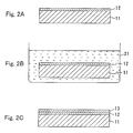
- Figures 2A to 2C are cross-sectional views showing another example of production processes in a method of the present invention.
- Figures 9A to 9C are cross-sectional views showing still another example of production processes in a method of the present invention.
- Figure 10 is a graph showing another example of current-voltage characteristics with respect to a pn junction produced by a method of the present invention and a pn junction produced by a method for producing a semiconductor device in a comparative example.
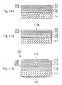
- Figures 11A to 11C are cross-sectional views showing still another example of production processes in a method of the present invention.
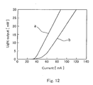
- Figure 12 is a graph showing still another example of current-light output characteristics with respect to a semiconductor laser produced by a method of the present invention and a semiconductor laser in a comparative example.
- Embodiment 1 an example of a method for producing a semiconductor device of the present invention will be described.
- Figures 2A to 2C show production processes in the method of Embodiment 1.
- a first semiconductor layer 12 made of a Group III nitride-based compound semiconductor is grown on a substrate 11.
- the first semiconductor layer 12 can be formed, for example, by metalorganic vapor phase epitaxy (MOVPE), hydride vapor phase epitaxy (HVPE), or molecular beam epitaxy (MBE).
- MOVPE metalorganic vapor phase epitaxy
- HVPE hydride vapor phase epitaxy
- MBE molecular beam epitaxy
- the first semiconductor layer 12 is formed in a reaction apparatus such as an MOVPE apparatus, an HVPE apparatus, or an MBE apparatus.
- a sapphire substrate or a substrate made of a Group III nitride-based compound semiconductor can be used as the substrate 11.
- the first semiconductor layer 12 is made of a Group III nitride-based compound semiconductor, i.e., a Group III-V compound semiconductor containing nitrogen as a Group V element.
- a Group III element at least one element selected from the group consisting of Ga, Al, and In can be used.
- the first semiconductor layer 12 may contain arsenic or phosphorus in addition to nitrogen, as the Group V element. More specifically, as a material for the first semiconductor layer 12, a semiconductor represented by Ga x In Y Al 1-X-Y N (0 ⁇ X ⁇ 1, 0 ⁇ Y ⁇ 1, X+Y ⁇ 1) can be used.
- the first semiconductor layer 12 may contain a dopant. Further, another semiconductor layer made of a Group III nitride-based compound semiconductor may be formed between the substrate 11 and the first semiconductor layer 12.
- the substrate 11 with the first semiconductor layer 12 formed thereon is taken out of the reaction apparatus and processed since an oxide layer and imparities adhere to the surface of the first semiconductor layer 12.
- the first semiconductor layer 12 is soaked in an alkaline aqueous solution 21 under the condition that a current is not flowing through the first semiconductor layer 12 (Process (a)). More specifically, the first semiconductor layer 12 is soaked in the solution under the condition that light having energy with a forbidden band width or larger of the first semiconductor layer 12 is not radiated to the first semiconductor layer 12.
- the alkaline aqueous solution include a potassium hydroxide aqueous solution, a sodium hydroxide aqueous solution, or an ammonia aqueous solution.
- a preferable pH value is varied depending upon the material of the first semiconductor layer 12 and the processing conditions.
- an alkaline aqueous solution for example, with a pH value of about 9 to 13 can be used.
- the temperature of the alkaline aqueous solution is in a range of 20°C to 130°C.
- the time for soaking the first semiconductor layer 12 in the alkaline aqueous solution is varied depending upon the pH thereof. It may be 1 to 10 minutes, for example. Because of Process (a), an oxide layer and impurities adhering to the surface of the first semiconductor layer 12 can be removed without etching the first semiconductor layer 12 excessively.
- the first semiconductor layer 12 is heated in gas containing nitrogen atoms (heating process).
- This heating process can be conducted by placing the first semiconductor layer 12 in the reaction apparatus, and introducing gas containing nitrogen atoms into the reaction apparatus while heating the substrate 11. More specifically, an MOVPE apparatus, an HVPE apparatus, or an MBE apparatus can be used.
- the heating temperature is in a range of 500°C to 1000°C, and more preferably at a temperature in a range of 600° to 900°C.
- the heating process may be omitted.
- Process (b) is conducted without exposing the second semiconductor layer 13 to the air after the heating process. More specifically, after conducting the heating process in the reaction apparatus, the process (b) should be conducted in the same apparatus.
- the second semiconductor layer 13 can be formed by a method similar to that of the first semiconductor layer 12.
- the second semiconductor layer 13 may be made of the same semiconductor as that of the first semiconductor layer 12, or may be made of a semiconductor different from that of the first semiconductor layer 12.
- the second semiconductor layer 13 may contain a dopant.
- the method for producing a semiconductor device in Embodiment 1 includes not only the above-mentioned production processes but also other production processes as described in examples, in accordance with a semiconductor device to be produced.
- an oxide layer and impurities adhering to the surface of the first semiconductor layer 12 are removed without etching it excessively. Therefore, the second semiconductor layer 13 with good crystallinity can be formed on the first semiconductor layer 12 exposed to the air.
- a heat treatment temperature in the heating process may be lower, so that the first semiconductor layer 12 is less influenced, and the second semiconductor layer 13 with particularly good crystallinity can be formed.
- Example 1 the case will be described with reference to Figures 9A to 9C in which a pn junction was formed by the method of Embodiment 1.
- an n-GaN layer (n-type GaN layer) 92 was grown on a sapphire substrate 91 in a reaction apparatus.
- the sapphire substrate 91 and the n-GaN layer 92 may be referred to as a substrate 93 collectively.
- the substrate 93 was placed in the MOVPE apparatus.
- the substrate 93 was heated to 1000°C, and a p-GaN layer (p-type GaN layer) 95 was grown on the n-GaN layer 92 by an MOVPE method, as shown in Figure 9C, whereby a pn junction 96 was formed.
- an oxide layer and impurities adhering to the surface of the n-GaN layer 92 were removed by using a potassium hydroxide aqueous solution. Therefore, an oxide layer and impurities can be removed efficiently while the surface of the n-GaN layer 92 was prevented from being roughened.
- an oxide layer is dissolved easily in a potassium hydroxide aqueous solution, so that the oxide layer on the surface of the n-GaN layer 92 can be removed efficiently.
- the p-GaN layer 95 is grown on the n-GaN layer 92 from which an oxide layer and impurities have been removed, the p-GaN layer 95 with good crystallinity can be formed.
- a pn junction in the comparative example was produced.
- the n-GaN layer 92 was subjected to surface treatment using phosphoric acid, which has been conducted conventionally. Thereafter, a p-GaN layer was formed to produce a pn junction.
- the pn junction 96 and the pn junction in the comparative example also were evaluated for characteristics.
- the surface of the p-GaN layer 95 was observed by photography with an optical microscope at a 1000-fold magnification. Consequently, the p-GaN layer 95 was found to have a mirror surface with little unevenness. It is considered that this is because the n-GaN layer 92 had a mirror surface with little unevenness, and the p-GaN layer 95 formed thereon also had a mirror surface.
- the concentrations of carbon and oxygen atoms at the interface of the pn junction 96 were 2 ⁇ 10 18 /cm 3 and 2 ⁇ 10 17 /cm 3 , respectively.
- the concentrations of carbon and oxygen atoms at the interface of the pn junction in the comparative example were 1 ⁇ 10 19 /cm 3 and 6 ⁇ 10 18 /cm 3 , respectively. From this, it was found that an oxide layer and impurities adhering to the surface of the n-GaN layer 92 were removed effectively by the surface treatment in Example 4, and the surface of the n-GaN layer 92 was cleaned effectively.
- Figure 10 shows current-voltage characteristics (line a) of the pn junction 96 and current voltage characteristics (line b) in the comparative example.
- a rise voltage of the pn junction 96 was 3.4 volts
- a rise voltage of the pn junction in the comparative example was 4.1 volts. From this, it can be understood that a satisfactory pn junction, which was not realized by the conventional surface treatment, was formed by the method of Example 4. The reason for this is considered that the surface of the n-GaN layer 92 was cleaned effectively.
- the specific resistance of the p-GaN layer was measured to be 0.3 ⁇ cm in the case of the pn junction in the comparative example, whereas the specific resistance of the p-GaN layer was measured to be 0.1 ⁇ cm in the case of the pn junction 96. From this, it was found that the p-GaN layer 92 with good crystallinity was formed by the surface treatment in Example 1.
- Example 1 According to the method of Example 1, the same effects can be obtained even when a sodium hydroxide aqueous solution or an ammonia aqueous solution is used in place of potassium hydroxide aqueous solution.
- Example 2 the case will be described with reference to Figures 11A to 11C in which a semiconductor laser with a current confinement layer was produced by the method of Embodiment 1.
- a substrate 111 made of n-type GaN was prepared.
- the substrate 111 was produced by growing an n-GaN layer on a sapphire substrate, and removing the sapphire substrate by polishing. Then, the surface of the substrate 111 was cleaned under the same conditions as those in Example 1. More specifically, the substrate 111 was subjected to heat treatment in an atmosphere of mixed gas (ammonia and hydrogen gas) in an MOVPE apparatus.
- mixed gas ammonia and hydrogen gas
- “slm” denotes a unit of a flow rate
- “1 slm” means that 1 L of gas in a standard state is allowed to flow for one minute.
- a cladding layer 112 (thickness: 1 ⁇ m) made of n-type AlGaN, a light guide layer 113 (thickness: 0.3 ⁇ m) made of n-type GaN, an active layer 114 made of InGaN, a light guide layer 115 (thickness: 0.05 ⁇ m) made of p-type GaN, a first p-AlGaN cladding layer 116 (thickness: 0.05 ⁇ m) made of p-type AlGaN, and a current confinement layer 117 (thickness: 0.5 ⁇ m) made of n-type AlGaN were formed on the substrate 111 successively by an MOVPE method.
- the atomic ratio between Al and Ga in the cladding layer 112 was set at 10 : 90.
- the active layer 114 had a multi-quantum well structure. More specifically, the active layer 114 is composed of a barrier layer (thickness: 3 nm, not shown) made of InGaN, and a well layer (thickness: 6 nm, not shown) made of InGaN.
- the atomic ratio between In and Ga in the barrier layer was set at 3 : 97, and the atomic ratio between In and Ga in the well layer was set at 15 : 85.
- the substrate 111 was taken out of the MOVPE apparatus, and an opening 117h in a stripe shape (width: 2 ⁇ m) was formed in the current confinement layer 117 by etching, as shown in Figure 11B.
- “slm” denotes a unit of a flow rate
- “1 slm” means that 1 L of gas in a standard state is allowed to flow for one minute.
- a second p-AlGaN cladding layer 118 (thickness: 1 ⁇ m) made of p-type AlGaN and a contact layer 119 (thickness: 0.1 ⁇ m) made of p-type GaN were formed successively on the first p-AlGaN cladding layer 116 and the current confinement layer 117 by an MOVPE method.
- the atomic ratio between Al and Ga in the p-AlGaN cladding layer 118 was set at 10 : 90.
- an n-side electrode 120 was formed on the back surface of the substrate 111, and a p-side electrode 121 was formed on the contact layer 119, whereby a semiconductor laser (semiconductor device) 122 was produced.
- a semiconductor laser was produced under the same conditions as those in the semiconductor laser 122 except that the substrate 111 and the current confinement layer 117 were subjected to surface treatment by using phosphoric acid, which has been used conventionally.
- this semiconductor laser will be referred to as a semiconductor laser in the comparative example.
- the substrate 111 and the current confinement layer 117 were subjected to heat treatment in an atmosphere of mixed gas (ammonia and hydrogen gas) after the surface treatment by potassium hydroxide aqueous solution. Therefore, water molecules, which adhere to the substrate 111 and the current confinement layer 117 when they are soaked in the potassium hydroxide aqueous solution, can be removed, and the surfaces of the substrate 111 and the current confinement layer 117 can be cleaned particularly. Consequently, the crystallinity of a Group III nitride-based compound semiconductor grown on the substrate 111 can be rendered particularly satisfactory.
- mixed gas ammonia and hydrogen gas
- Figure 12 shows current-light output characteristics (line a) of the semiconductor laser 122 and current-light output characteristics (line b) of the semiconductor laser in the comparative example. It is understood from Figure 12 that a threshold current and a working current of the semiconductor laser 122 are smaller than those of the semiconductor laser in the comparative example. It is considered that this is because the surface of the first p-AlGaN cladding layer 116 was cleaned sufficiently, so that the second p-AlGaN cladding layer 118 with good crystallinity was formed; as a result, an electrical resistance and a light loss at the interface between the first p-AlGaN cladding layer 116 and the second p-AlGaN cladding layer 117 were reduced.
- a durability test was conducted with respect to the semiconductor laser 122 and the semiconductor laser in the comparative example.
- the durability test was conducted by operating a plurality of semiconductor lasers at a temperature of 25°C and a constant light output (30 mW). About half of the semiconductor lasers in the comparative example were disabled after 1000 hours from the commencement of the durability test. The remaining semiconductor lasers also were degraded considerably in device characteristics (i.e., a working current increased by 60% on average). On the other hand, all the semiconductor lasers 122 were operational even after 1000 hours from the commencement of the durability test, and a working current increased by 2% on average. Thus, the reliability of the semiconductor laser in Example 1 was enhanced remarkably.
- the surface of a first semiconductor layer made of nitride-based compound semiconductor can be cleaned while the flatness of the surface is maintained. Therefore, according to the method of the present invention, a second semiconductor layer made of a nitride-based compound semiconductor with good crystallinity can be grown on the first semiconductor layer. Consequently, a semiconductor device with good characteristics and high reliability can be produced.
- the method for producing a semiconductor device of the present invention is applicable to a semiconductor device in which at least two Group III nitride-based compound semiconductors are layered.
- the method is applicable to a semiconductor laser, a light-emitting diode, an FET, and the like.
Landscapes
- Engineering & Computer Science (AREA)
- Physics & Mathematics (AREA)
- General Physics & Mathematics (AREA)
- Condensed Matter Physics & Semiconductors (AREA)
- Power Engineering (AREA)
- Microelectronics & Electronic Packaging (AREA)
- Computer Hardware Design (AREA)
- Manufacturing & Machinery (AREA)
- Chemical & Material Sciences (AREA)
- Nanotechnology (AREA)
- Materials Engineering (AREA)
- Crystallography & Structural Chemistry (AREA)
- Life Sciences & Earth Sciences (AREA)
- Optics & Photonics (AREA)
- Biophysics (AREA)
- Semiconductor Lasers (AREA)
- Led Devices (AREA)
- Drying Of Semiconductors (AREA)
- Weting (AREA)
- Junction Field-Effect Transistors (AREA)
Abstract
A method for producing a semiconductor device of the present invention comprises:
(a) soaking a first semiconductor layer made of a Group III nitride-based compound semiconductor in an alkaline aqueous solution under a condition that a current is not flowing through the first semiconductor layer; and
(b) after the process (a), growing a second semiconductor layer made of a Group III nitride-based compound semiconductor on the first semiconductor layer.
Description
- The present invention relates to a method for producing a semiconductor device using a Group III nitride-based compound semiconductor.
- In recent years, a blue-light semiconductor laser using a Group III nitride semiconductor such as GaN has been extensively developed. Such a blue-light semiconductor laser can be used as a light source for an optical disk reproduction apparatus.
- In the case of producing a blue-light semiconductor laser, it is sometimes required alternately to repeat crystal growth in a vacuum apparatus and an operation in the air. For example, in the case of producing an embedded ridge type laser, a Group III nitride semiconductor layer is formed on a substrate in a vacuum apparatus, and then, the substrate is exposed to the air to form a current confinement layer. Thereafter, the substrate is placed again in the vacuum apparatus, and another Group III nitride semiconductor layer is grown on the Group III nitride semiconductor layer. In this case, an oxide layer is formed or impurities adhere to the surface of the first semiconductor layer during exposure to the air.
Therefore, it is particularly important to conduct surface treatment of the first semiconductor layer after exposure to the air. In the surface treatment, it is required to remove the oxide layer and the impurities adhering to the surface of the semiconductor layer while preventing the surface of the semiconductor layer from being roughened. - Conventionally, a method for treating the surface of a Group III nitride semiconductor layer has been reported. For example, a method has been reported for treating a substrate, on which a semiconductor layer made of GaN is formed by epitaxial growth, (hereinafter, referred to as an "epitaxial substrate"), using heated concentrated phosphoric acid. Further, a method has been reported for electrolytically etching an epitaxial substrate in an alkaline solution. Further, a method has been reported for etching an epitaxial substrate soaked in an alkaline solution by irradiating light having energy larger than the bandgap energy of GaN thereto (
JP 9(1997)-232681 - However, according to a method for conducting surface treatment by using heated concentrated phosphoric acid, the surface flatness of a semiconductor layer is decreased due to the inconsistencies in the temperature of the heated concentrated phosphoric acid. Further, according to a method for etching in an alkaline solution, the surface flatness of a semiconductor layer also is decreased due to the local irregularities in a current or light irradiation. Such a decrease in the surface flatness of a semiconductor layer decreases the crystallinity of another Group III nitride semiconductor grown on an epitaxial substrate, which degrades the physical and electrical characteristics of a semiconductor device.
- Therefore, with the foregoing in mind, it is an object of the present invention to provide a method for producing a semiconductor device with high performance and reliability.
- The method for producing a semiconductor device of the present invention includes: (a) soaking a first semiconductor layer made of a Group III nitride-based compound semiconductor in an alkaline aqueous solution under a condition that a current is not flowing through the first semiconductor layer; and (b) after the process (a), growing a second semiconductor layer made of a Group III nitride-based compound semiconductor on the first semiconductor layer. According to the method, an oxide layer and impurities adhering to the surface of the first semiconductor layer can be removed without degrading the flatness of the surface of the first semiconductor layer. Therefore, according to the method, the semiconductor layer with good crystallinity can be grown, whereby a semiconductor device with high performance and reliability can be produced.
- The method further may include, after the process (a) and before the process (b), a heating process of heating the first semiconductor layer in gas containing nitrogen atoms. According to this structure, an oxide layer and moisture adhering to the surface of the first semiconductor layer during the process (a) can be removed, so that the second semiconductor layer with particularly good crystallinity can be formed.
- According to the method, the gas may contain at least one selected from the group consisting of nitrogen gas, ammonia, hydrazine, and a hydrazine derivative.
- According to the method, the first semiconductor layer may be heated at a temperature in a range of 500°C to 1000°C in the heating process.
- This and other advantages of the present invention will become apparent to those skilled in the art upon reading and understanding the following detailed description with reference to the accompanying figures.
- Figures 2A to 2C are cross-sectional views showing another example of production processes in a method of the present invention.
- Figures 9A to 9C are cross-sectional views showing still another example of production processes in a method of the present invention.
- Figure 10 is a graph showing another example of current-voltage characteristics with respect to a pn junction produced by a method of the present invention and a pn junction produced by a method for producing a semiconductor device in a comparative example.
- Figures 11A to 11C are cross-sectional views showing still another example of production processes in a method of the present invention.
- Figure 12 is a graph showing still another example of current-light output characteristics with respect to a semiconductor laser produced by a method of the present invention and a semiconductor laser in a comparative example.
- Hereinafter, the present invention will be described by way of illustrative embodiments with reference to the drawings. In the following description, a reaction apparatus will be omitted in the drawings except for Figure 3.
- In
Embodiment 1, an example of a method for producing a semiconductor device of the present invention will be described. - Figures 2A to 2C show production processes in the method of
Embodiment 1. According to the method ofEmbodiment 1, first as shown in Figure 2A, afirst semiconductor layer 12 made of a Group III nitride-based compound semiconductor is grown on asubstrate 11. Thefirst semiconductor layer 12 can be formed, for example, by metalorganic vapor phase epitaxy (MOVPE), hydride vapor phase epitaxy (HVPE), or molecular beam epitaxy (MBE). Thefirst semiconductor layer 12 is formed in a reaction apparatus such as an MOVPE apparatus, an HVPE apparatus, or an MBE apparatus. - As the
substrate 11, a sapphire substrate or a substrate made of a Group III nitride-based compound semiconductor can be used. - The
first semiconductor layer 12 is made of a Group III nitride-based compound semiconductor, i.e., a Group III-V compound semiconductor containing nitrogen as a Group V element. As the Group III element, at least one element selected from the group consisting of Ga, Al, and In can be used. Further, thefirst semiconductor layer 12 may contain arsenic or phosphorus in addition to nitrogen, as the Group V element. More specifically, as a material for thefirst semiconductor layer 12, a semiconductor represented by GaxInYAl1-X-Y N (0≤X≤1, 0≤Y≤1, X+Y≤1) can be used. Thefirst semiconductor layer 12 may contain a dopant. Further, another semiconductor layer made of a Group III nitride-based compound semiconductor may be formed between thesubstrate 11 and thefirst semiconductor layer 12. - Thereafter, the
substrate 11 with thefirst semiconductor layer 12 formed thereon is taken out of the reaction apparatus and processed since an oxide layer and imparities adhere to the surface of thefirst semiconductor layer 12. - Thereafter, as shown in Figure 2B, the
first semiconductor layer 12 is soaked in an alkalineaqueous solution 21 under the condition that a current is not flowing through the first semiconductor layer 12 (Process (a)). More specifically, thefirst semiconductor layer 12 is soaked in the solution under the condition that light having energy with a forbidden band width or larger of thefirst semiconductor layer 12 is not radiated to thefirst semiconductor layer 12. Examples of the alkaline aqueous solution include a potassium hydroxide aqueous solution, a sodium hydroxide aqueous solution, or an ammonia aqueous solution. A preferable pH value is varied depending upon the material of thefirst semiconductor layer 12 and the processing conditions. However, an alkaline aqueous solution, for example, with a pH value of about 9 to 13 can be used. Further, it is preferable that the temperature of the alkaline aqueous solution is in a range of 20°C to 130°C. The time for soaking thefirst semiconductor layer 12 in the alkaline aqueous solution is varied depending upon the pH thereof. It may be 1 to 10 minutes, for example. Because of Process (a), an oxide layer and impurities adhering to the surface of thefirst semiconductor layer 12 can be removed without etching thefirst semiconductor layer 12 excessively. - After Process (a), the
first semiconductor layer 12 is heated in gas containing nitrogen atoms (heating process). This heating process can be conducted by placing thefirst semiconductor layer 12 in the reaction apparatus, and introducing gas containing nitrogen atoms into the reaction apparatus while heating thesubstrate 11. More specifically, an MOVPE apparatus, an HVPE apparatus, or an MBE apparatus can be used. - In this heating process, since a thin oxide layer formed after Process (a) on the surface of the
first semiconductor layer 12 merely is removed, the heating temperature is in a range of 500°C to 1000°C, and more preferably at a temperature in a range of 600° to 900°C. The heating process may be omitted. - Next, a
second semiconductor layer 13 made of a Group III nitride-based compound semiconductor is grown on the first semiconductor layer 12 (Process (b)). Process (b) is conducted without exposing thesecond semiconductor layer 13 to the air after the heating process. More specifically, after conducting the heating process in the reaction apparatus, the process (b) should be conducted in the same apparatus. - The
second semiconductor layer 13 can be formed by a method similar to that of thefirst semiconductor layer 12. Thesecond semiconductor layer 13 may be made of the same semiconductor as that of thefirst semiconductor layer 12, or may be made of a semiconductor different from that of thefirst semiconductor layer 12. Thesecond semiconductor layer 13 may contain a dopant. - The method for producing a semiconductor device in
Embodiment 1 includes not only the above-mentioned production processes but also other production processes as described in examples, in accordance with a semiconductor device to be produced. According to the method ofEmbodiment 1, an oxide layer and impurities adhering to the surface of thefirst semiconductor layer 12 are removed without etching it excessively. Therefore, thesecond semiconductor layer 13 with good crystallinity can be formed on thefirst semiconductor layer 12 exposed to the air. In particular, according to the method ofEmbodiment 1, a heat treatment temperature in the heating process may be lower, so that thefirst semiconductor layer 12 is less influenced, and thesecond semiconductor layer 13 with particularly good crystallinity can be formed. - Hereinafter, the present invention will be described in more detail by way of illustrative examples.
- In Example 1, the case will be described with reference to Figures 9A to 9C in which a pn junction was formed by the method of
Embodiment 1. - First, as shown in Figure 9A, an n-GaN layer (n-type GaN layer) 92 was grown on a
sapphire substrate 91 in a reaction apparatus. Hereinafter, thesapphire substrate 91 and the n-GaN layer 92 may be referred to as asubstrate 93 collectively. - Next, the
substrate 93 was taken out of the reaction apparatus, and washed with an organic solvent for removal of dust and degreasing. Thereafter, as shown in Figure 9B, thesubstrate 93 was soaked in a potassium hydroxide aqueous solution 94 (pH = 13, 90°C) for 5 minutes, whereby an oxide layer and impurities adhering to the surface of the n-GaN layer 92 were removed. In this process, if a current had flowed through the n-GaN layer 92, an etching rate of the n-GaN layer 92 would have been increased, and the surface of the n-GaN layer 92 would have been roughened. So, in the process of Figure 9B, a current was prevented from flowing through the potassium hydroxideaqueous solution 94, and light with energy larger than a forbidden band width of the n-GaN layer 92 was prevented from being radiated to the n-GaN layer 92. According to the surface treatment in Figure 9B, a thin oxide layer and impurities adhering to the surface of the n-GaN layer 92 merely are removed, so that only a very thin layer in the vicinity of the surface of the n-GaN layer 92 should be removed. - Thereafter, the
substrate 93 was placed in the MOVPE apparatus. Thesubstrate 93 was heated to 1000°C, and a p-GaN layer (p-type GaN layer) 95 was grown on the n-GaN layer 92 by an MOVPE method, as shown in Figure 9C, whereby apn junction 96 was formed. - According to the method of Example 1, an oxide layer and impurities adhering to the surface of the n-
GaN layer 92 were removed by using a potassium hydroxide aqueous solution. Therefore, an oxide layer and impurities can be removed efficiently while the surface of the n-GaN layer 92 was prevented from being roughened. In particular, an oxide layer is dissolved easily in a potassium hydroxide aqueous solution, so that the oxide layer on the surface of the n-GaN layer 92 can be removed efficiently. According to the method of Example 4, since the p-GaN layer 95 is grown on the n-GaN layer 92 from which an oxide layer and impurities have been removed, the p-GaN layer 95 with good crystallinity can be formed. - Further, for comparison, a pn junction in the comparative example was produced. In this comparative example, the n-
GaN layer 92 was subjected to surface treatment using phosphoric acid, which has been conducted conventionally. Thereafter, a p-GaN layer was formed to produce a pn junction. Thepn junction 96 and the pn junction in the comparative example also were evaluated for characteristics. - Regarding the
pn junction 96, the surface of the p-GaN layer 95 was observed by photography with an optical microscope at a 1000-fold magnification. Consequently, the p-GaN layer 95 was found to have a mirror surface with little unevenness. It is considered that this is because the n-GaN layer 92 had a mirror surface with little unevenness, and the p-GaN layer 95 formed thereon also had a mirror surface. - Further, impurities at the junction interface were evaluated by secondary ion mass spectrometry (SIMS). Consequently, the concentrations of carbon and oxygen atoms at the interface of the pn junction 96 (interface between the n-
GaN layer 92 and the p-GaN layer 95) were 2 × 10¹⁸/cm3 and 2 × 10¹⁷/cm3, respectively. On the other hand, the concentrations of carbon and oxygen atoms at the interface of the pn junction in the comparative example were 1 × 10¹⁹/cm3 and 6 × 10¹⁸/cm3, respectively. From this, it was found that an oxide layer and impurities adhering to the surface of the n-GaN layer 92 were removed effectively by the surface treatment in Example 4, and the surface of the n-GaN layer 92 was cleaned effectively. - Next, the
pn junction 96 and the pn junction in the comparative example were measured for current-voltage characteristics. Figure 10 shows current-voltage characteristics (line a) of thepn junction 96 and current voltage characteristics (line b) in the comparative example. As shown in Figure 10, a rise voltage of thepn junction 96 was 3.4 volts, whereas a rise voltage of the pn junction in the comparative example was 4.1 volts. From this, it can be understood that a satisfactory pn junction, which was not realized by the conventional surface treatment, was formed by the method of Example 4. The reason for this is considered that the surface of the n-GaN layer 92 was cleaned effectively. - Further, the specific resistance of the p-GaN layer was measured to be 0.3 Ω·cm in the case of the pn junction in the comparative example, whereas the specific resistance of the p-GaN layer was measured to be 0.1 Ω·cm in the case of the
pn junction 96. From this, it was found that the p-GaN layer 92 with good crystallinity was formed by the surface treatment in Example 1. - According to the method of Example 1, the same effects can be obtained even when a sodium hydroxide aqueous solution or an ammonia aqueous solution is used in place of potassium hydroxide aqueous solution.
- In Example 2, the case will be described with reference to Figures 11A to 11C in which a semiconductor laser with a current confinement layer was produced by the method of
Embodiment 1. - First, a
substrate 111 made of n-type GaN was prepared. Thesubstrate 111 was produced by growing an n-GaN layer on a sapphire substrate, and removing the sapphire substrate by polishing. Then, the surface of thesubstrate 111 was cleaned under the same conditions as those in Example 1. More specifically, thesubstrate 111 was subjected to heat treatment in an atmosphere of mixed gas (ammonia and hydrogen gas) in an MOVPE apparatus. - Next, the
substrate 111 was subjected to surface treatment using potassium hydroxide aqueous solution under the same conditions as those in Example 1. Thereafter, thesubstrate 111 was placed in an MOVPE apparatus, and thesubstrate 111 was subjected to heat treatment in an atmosphere of mixed gas (hydrogen gas: ammonia = 15 : 4 (ratio of flow rate)) of 1.01 ×10⁵ Pa (1 atmospheric pressure). More specifically, the flow rates of hydrogen gas and ammonia were set at 15 slm and 4 slm, respectively. Here, "slm" denotes a unit of a flow rate, and "1 slm" means that 1 L of gas in a standard state is allowed to flow for one minute. - After the heat treatment, as shown in Figure 11B, a cladding layer 112 (thickness: 1 µm) made of n-type AlGaN, a light guide layer 113 (thickness: 0.3 µm) made of n-type GaN, an
active layer 114 made of InGaN, a light guide layer 115 (thickness: 0.05 µm) made of p-type GaN, a first p-AlGaN cladding layer 116 (thickness: 0.05 µm) made of p-type AlGaN, and a current confinement layer 117 (thickness: 0.5 µm) made of n-type AlGaN were formed on thesubstrate 111 successively by an MOVPE method. The atomic ratio between Al and Ga in thecladding layer 112 was set at 10 : 90. Theactive layer 114 had a multi-quantum well structure. More specifically, theactive layer 114 is composed of a barrier layer (thickness: 3 nm, not shown) made of InGaN, and a well layer (thickness: 6 nm, not shown) made of InGaN. The atomic ratio between In and Ga in the barrier layer was set at 3 : 97, and the atomic ratio between In and Ga in the well layer was set at 15 : 85. - Next, the
substrate 111 was taken out of the MOVPE apparatus, and anopening 117h in a stripe shape (width: 2 µm) was formed in thecurrent confinement layer 117 by etching, as shown in Figure 11B. - Then, the
substrate 111 was subjected to surface treatment using potassium hydroxide aqueous solution under the same conditions as those in Example 1. Thereafter, thesubstrate 111 was placed in the MOVPE apparatus again. Then, heat treatment was conducted in an atmosphere of mixed gas (hydrogen gas: ammonia = 15 : 4 (ratio of flow rate)) of 1.01 ×10⁵ Pa (1 atmospheric pressure). More specifically, the flow rates of hydrogen gas and ammonia were set at 15 slm and 4 slm, respectively. Here, "slm" denotes a unit of a flow rate, and "1 slm" means that 1 L of gas in a standard state is allowed to flow for one minute. - After the heat treatment, as shown in Figure 11C, a second p-AlGaN cladding layer 118 (thickness: 1 µm) made of p-type AlGaN and a contact layer 119 (thickness: 0.1 µm) made of p-type GaN were formed successively on the first p-
AlGaN cladding layer 116 and thecurrent confinement layer 117 by an MOVPE method. The atomic ratio between Al and Ga in the p-AlGaN cladding layer 118 was set at 10 : 90. - Finally, as shown in Figure 11C, an n-
side electrode 120 was formed on the back surface of thesubstrate 111, and a p-side electrode 121 was formed on thecontact layer 119, whereby a semiconductor laser (semiconductor device) 122 was produced. - On the other hand, as a comparative example, a semiconductor laser was produced under the same conditions as those in the
semiconductor laser 122 except that thesubstrate 111 and thecurrent confinement layer 117 were subjected to surface treatment by using phosphoric acid, which has been used conventionally. Hereinafter, this semiconductor laser will be referred to as a semiconductor laser in the comparative example. - According to the method of Example 1, the
substrate 111 and thecurrent confinement layer 117 were subjected to heat treatment in an atmosphere of mixed gas (ammonia and hydrogen gas) after the surface treatment by potassium hydroxide aqueous solution. Therefore, water molecules, which adhere to thesubstrate 111 and thecurrent confinement layer 117 when they are soaked in the potassium hydroxide aqueous solution, can be removed, and the surfaces of thesubstrate 111 and thecurrent confinement layer 117 can be cleaned particularly. Consequently, the crystallinity of a Group III nitride-based compound semiconductor grown on thesubstrate 111 can be rendered particularly satisfactory. - Figure 12 shows current-light output characteristics (line a) of the
semiconductor laser 122 and current-light output characteristics (line b) of the semiconductor laser in the comparative example. It is understood from Figure 12 that a threshold current and a working current of thesemiconductor laser 122 are smaller than those of the semiconductor laser in the comparative example. It is considered that this is because the surface of the first p-AlGaN cladding layer 116 was cleaned sufficiently, so that the second p-AlGaN cladding layer 118 with good crystallinity was formed; as a result, an electrical resistance and a light loss at the interface between the first p-AlGaN cladding layer 116 and the second p-AlGaN cladding layer 117 were reduced. - A durability test was conducted with respect to the
semiconductor laser 122 and the semiconductor laser in the comparative example. The durability test was conducted by operating a plurality of semiconductor lasers at a temperature of 25°C and a constant light output (30 mW). About half of the semiconductor lasers in the comparative example were disabled after 1000 hours from the commencement of the durability test. The remaining semiconductor lasers also were degraded considerably in device characteristics (i.e., a working current increased by 60% on average). On the other hand, all thesemiconductor lasers 122 were operational even after 1000 hours from the commencement of the durability test, and a working current increased by 2% on average. Thus, the reliability of the semiconductor laser in Example 1 was enhanced remarkably. - As described above, according to the method for producing a semiconductor device of the present invention, the surface of a first semiconductor layer made of nitride-based compound semiconductor can be cleaned while the flatness of the surface is maintained. Therefore, according to the method of the present invention, a second semiconductor layer made of a nitride-based compound semiconductor with good crystallinity can be grown on the first semiconductor layer. Consequently, a semiconductor device with good characteristics and high reliability can be produced.
- The method for producing a semiconductor device of the present invention is applicable to a semiconductor device in which at least two Group III nitride-based compound semiconductors are layered. For example, the method is applicable to a semiconductor laser, a light-emitting diode, an FET, and the like.
Claims (4)
- A method for producing a semiconductor device, comprising:(a) soaking a first semiconductor layer made of a Group III nitride-based compound semiconductor in an alkaline aqueous solution under a condition that a current is not flowing through the first semiconductor layer; and(b) after the process (a), growing a second semiconductor layer made of a Group III nitride-based compound semiconductor on the first semiconductor layer.
- A method for producing a semiconductor device according to claim 1, further comprising, after the process (a) and before the process (b), a heating process of heating the first semiconductor laser in gas containing nitrogen atoms.
- A method for producing a semiconductor device according to claim 2, wherein the gas contains at least one selected from the group consisting of nitrogen gas, ammonia, hydrazine, and a hydrazine derivative.
- A method for producing a semiconductor device according to claim 2 or 3, wherein the first semiconductor layer is heated at a temperature in a range of 500°C to 1000°C in the heating process.
Applications Claiming Priority (3)
| Application Number | Priority Date | Filing Date | Title |
|---|---|---|---|
| JP36987199 | 1999-12-27 | ||
| JP2000027453 | 2000-02-04 | ||
| EP00128255A EP1113485A3 (en) | 1999-12-27 | 2000-12-22 | Method for producing a semiconductor device |
Related Parent Applications (1)
| Application Number | Title | Priority Date | Filing Date |
|---|---|---|---|
| EP00128255A Division EP1113485A3 (en) | 1999-12-27 | 2000-12-22 | Method for producing a semiconductor device |
Publications (1)
| Publication Number | Publication Date |
|---|---|
| EP1727189A2 true EP1727189A2 (en) | 2006-11-29 |
Family
ID=26582166
Family Applications (2)
| Application Number | Title | Priority Date | Filing Date |
|---|---|---|---|
| EP06018320A Withdrawn EP1727189A2 (en) | 1999-12-27 | 2000-12-22 | Method for producing a semiconductor device |
| EP00128255A Withdrawn EP1113485A3 (en) | 1999-12-27 | 2000-12-22 | Method for producing a semiconductor device |
Family Applications After (1)
| Application Number | Title | Priority Date | Filing Date |
|---|---|---|---|
| EP00128255A Withdrawn EP1113485A3 (en) | 1999-12-27 | 2000-12-22 | Method for producing a semiconductor device |
Country Status (4)
| Country | Link |
|---|---|
| US (1) | US6673702B2 (en) |
| EP (2) | EP1727189A2 (en) |
| JP (1) | JP2001291703A (en) |
| KR (1) | KR100440705B1 (en) |
Families Citing this family (13)
| Publication number | Priority date | Publication date | Assignee | Title |
|---|---|---|---|---|
| JP4037154B2 (en) * | 2002-04-15 | 2008-01-23 | 松下電器産業株式会社 | Plasma processing method |
| US9279193B2 (en) | 2002-12-27 | 2016-03-08 | Momentive Performance Materials Inc. | Method of making a gallium nitride crystalline composition having a low dislocation density |
| KR100576850B1 (en) * | 2003-10-28 | 2006-05-10 | 삼성전기주식회사 | Manufacturing method of nitride based semiconductor light emitting device |
| US7148149B2 (en) * | 2003-12-24 | 2006-12-12 | Matsushita Electric Industrial Co., Ltd. | Method for fabricating nitride-based compound semiconductor element |
| US7626217B2 (en) * | 2005-04-11 | 2009-12-01 | Cree, Inc. | Composite substrates of conductive and insulating or semi-insulating group III-nitrides for group III-nitride devices |
| US7446345B2 (en) * | 2005-04-29 | 2008-11-04 | Cree, Inc. | Light emitting devices with active layers that extend into opened pits |
| JP2006352075A (en) * | 2005-05-17 | 2006-12-28 | Sumitomo Electric Ind Ltd | Cleaning method and manufacturing method for nitride compound semiconductor, and compound semiconductor, and board |
| US20110018105A1 (en) * | 2005-05-17 | 2011-01-27 | Sumitomo Electric Industries, Ltd. | Nitride-based compound semiconductor device, compound semiconductor device, and method of producing the devices |
| US9331192B2 (en) * | 2005-06-29 | 2016-05-03 | Cree, Inc. | Low dislocation density group III nitride layers on silicon carbide substrates and methods of making the same |
| JP4967914B2 (en) * | 2006-08-22 | 2012-07-04 | 豊田合成株式会社 | Method for manufacturing light emitting device |
| DE102007019079A1 (en) * | 2007-01-26 | 2008-07-31 | Osram Opto Semiconductors Gmbh | Optoelectronic semiconductor chip producing method, involves forming epitaxial covering layer that is downstream of semiconductor section, and electrically activating p-doped region of section before or during formation of covering layer |
| JP5003527B2 (en) * | 2008-02-22 | 2012-08-15 | 住友電気工業株式会社 | Group III nitride light emitting device and method for fabricating group III nitride semiconductor light emitting device |
| JP4787891B2 (en) * | 2009-06-09 | 2011-10-05 | 住友電気工業株式会社 | Group III nitride crystal substrate for epitaxial layer formation, group III nitride crystal substrate with epitaxial layer, and semiconductor device |
Family Cites Families (13)
| Publication number | Priority date | Publication date | Assignee | Title |
|---|---|---|---|---|
| US4335506A (en) * | 1980-08-04 | 1982-06-22 | International Business Machines Corporation | Method of forming aluminum/copper alloy conductors |
| US5631190A (en) * | 1994-10-07 | 1997-05-20 | Cree Research, Inc. | Method for producing high efficiency light-emitting diodes and resulting diode structures |
| JP3575859B2 (en) | 1995-03-10 | 2004-10-13 | 株式会社東芝 | Semiconductor substrate surface treatment method and surface treatment device |
| JPH0945670A (en) * | 1995-07-29 | 1997-02-14 | Hewlett Packard Co <Hp> | Vapor phase etching method of group iiinitrogen crystal and re-deposition process method |
| WO1997008356A2 (en) | 1995-08-18 | 1997-03-06 | The Regents Of The University Of California | Modified metalorganic chemical vapor deposition of group iii-v thin layers |
| JPH09232681A (en) | 1996-02-22 | 1997-09-05 | Hitachi Ltd | Nitride compd. semiconductor optical device |
| JP3344287B2 (en) | 1996-08-30 | 2002-11-11 | 住友電気工業株式会社 | Method for cleaning surface of II-VI compound semiconductor crystal |
| TW349132B (en) | 1996-08-30 | 1999-01-01 | Sumitomo Electric Industries | Surface cleaning method of II-VI Group compound semiconductor crystal |
| JPH10163114A (en) * | 1996-11-29 | 1998-06-19 | Matsushita Electron Corp | Semiconductor device and manufacturing method thereof |
| TW385493B (en) * | 1997-08-04 | 2000-03-21 | Sumitomo Chemical Co | Method for manufacturing group III-V compound semiconductor |
| JP3794876B2 (en) * | 1998-09-09 | 2006-07-12 | 松下電器産業株式会社 | Manufacturing method of semiconductor device |
| JP2000183465A (en) * | 1998-12-18 | 2000-06-30 | Pioneer Electronic Corp | Method of manufacturing group iii nitride semiconductor element |
| GB2350927A (en) * | 1999-06-12 | 2000-12-13 | Sharp Kk | A method growing nitride semiconductor layer by molecular beam epitaxy |
-
2000
- 2000-12-22 EP EP06018320A patent/EP1727189A2/en not_active Withdrawn
- 2000-12-22 EP EP00128255A patent/EP1113485A3/en not_active Withdrawn
- 2000-12-26 US US09/748,436 patent/US6673702B2/en not_active Expired - Fee Related
- 2000-12-26 JP JP2000395312A patent/JP2001291703A/en active Pending
- 2000-12-27 KR KR10-2000-0082697A patent/KR100440705B1/en not_active IP Right Cessation
Also Published As
| Publication number | Publication date |
|---|---|
| US20010021572A1 (en) | 2001-09-13 |
| EP1113485A3 (en) | 2005-08-31 |
| KR20010078747A (en) | 2001-08-21 |
| US6673702B2 (en) | 2004-01-06 |
| KR100440705B1 (en) | 2004-07-15 |
| JP2001291703A (en) | 2001-10-19 |
| EP1113485A2 (en) | 2001-07-04 |
Similar Documents
| Publication | Publication Date | Title |
|---|---|---|
| JP3688843B2 (en) | Nitride semiconductor device manufacturing method | |
| US6829273B2 (en) | Nitride semiconductor layer structure and a nitride semiconductor laser incorporating a portion of same | |
| JP3470623B2 (en) | Method for growing nitride III-V compound semiconductor, method for manufacturing semiconductor device, and semiconductor device | |
| JP3433075B2 (en) | Method of manufacturing nitride semiconductor device | |
| US20010038656A1 (en) | Nitride semiconductor device | |
| US20050218414A1 (en) | 4H-polytype gallium nitride-based semiconductor device on a 4H-polytype substrate | |
| WO2008054994A2 (en) | Deep ultraviolet light emitting device and method for fabricating same | |
| EP1196971B1 (en) | Nitride semiconductor layer structure and a nitride semiconductor laser incorporating a portion of same | |
| US20100265976A1 (en) | Semiconductor layer structure | |
| EP1727189A2 (en) | Method for producing a semiconductor device | |
| JPH11251687A (en) | Manufacture of semiconductor and semiconductor device | |
| US20040179563A1 (en) | Semiconductor laser and process for manufacturing the same | |
| US6960482B2 (en) | Method of fabricating nitride semiconductor and method of fabricating semiconductor device | |
| JP2000082863A (en) | Manufacture of semiconductor light emitting element | |
| US7005685B2 (en) | Gallium-nitride-based compound semiconductor device | |
| KR20050061681A (en) | Gan based semiconductor light emitting diode and method of producing the same | |
| JP2999435B2 (en) | Semiconductor manufacturing method and semiconductor light emitting device | |
| EP1121735A1 (en) | Improved far-field nitride based semiconductor laser | |
| JPH08203862A (en) | Method for etching nitride compound semiconductor | |
| JP2002151415A (en) | Nitride-family semiconductor element, substrate therefor and method of manufacturing the same | |
| JP4419520B2 (en) | Semiconductor laser diode and manufacturing method thereof | |
| JPH1070082A (en) | Method of forming p-type nitride based iii-v compound semiconductor layer | |
| JP3927646B2 (en) | Gallium nitride compound semiconductor light emitting device and method for manufacturing the same | |
| JPH11274555A (en) | Semiconductor element | |
| JP2003179027A (en) | Method of etching nitride system compound semiconductor |
Legal Events
| Date | Code | Title | Description |
|---|---|---|---|
| PUAI | Public reference made under article 153(3) epc to a published international application that has entered the european phase |
Free format text: ORIGINAL CODE: 0009012 |
|
| 17P | Request for examination filed |
Effective date: 20060901 |
|
| AC | Divisional application: reference to earlier application |
Ref document number: 1113485 Country of ref document: EP Kind code of ref document: P |
|
| AK | Designated contracting states |
Kind code of ref document: A2 Designated state(s): DE FR GB |
|
| RAP1 | Party data changed (applicant data changed or rights of an application transferred) |
Owner name: PANASONIC CORPORATION |
|
| STAA | Information on the status of an ep patent application or granted ep patent |
Free format text: STATUS: THE APPLICATION HAS BEEN WITHDRAWN |
|
| 18W | Application withdrawn |
Effective date: 20090219 |