EP1717830B1 - Electromechanical micro-capacitor with variable capacity and process of manufacture of such a capacitor - Google Patents
Electromechanical micro-capacitor with variable capacity and process of manufacture of such a capacitor Download PDFInfo
- Publication number
- EP1717830B1 EP1717830B1 EP06354011A EP06354011A EP1717830B1 EP 1717830 B1 EP1717830 B1 EP 1717830B1 EP 06354011 A EP06354011 A EP 06354011A EP 06354011 A EP06354011 A EP 06354011A EP 1717830 B1 EP1717830 B1 EP 1717830B1
- Authority
- EP
- European Patent Office
- Prior art keywords
- micro
- electrode
- electrodes
- capacitor according
- capacitor
- Prior art date
- Legal status (The legal status is an assumption and is not a legal conclusion. Google has not performed a legal analysis and makes no representation as to the accuracy of the status listed.)
- Active
Links
Images


Classifications
-
- H—ELECTRICITY
- H01—ELECTRIC ELEMENTS
- H01G—CAPACITORS; CAPACITORS, RECTIFIERS, DETECTORS, SWITCHING DEVICES OR LIGHT-SENSITIVE DEVICES, OF THE ELECTROLYTIC TYPE
- H01G5/00—Capacitors in which the capacitance is varied by mechanical means, e.g. by turning a shaft; Processes of their manufacture
- H01G5/16—Capacitors in which the capacitance is varied by mechanical means, e.g. by turning a shaft; Processes of their manufacture using variation of distance between electrodes
- H01G5/18—Capacitors in which the capacitance is varied by mechanical means, e.g. by turning a shaft; Processes of their manufacture using variation of distance between electrodes due to change in inclination, e.g. by flexing, by spiral wrapping
Definitions
- the invention relates to an electromechanical micro-capacitor having a variable capacity as a function of an electrical operating voltage and comprising at least first and second electrodes, the first electrode being integral with a beam having two ends integral with a support. fixed on a substrate.
- Some electromechanical micro-capacitors with variable capacitance have an operation based on the variation of the gap between the two electrodes of the capacitor.
- the capacity of the capacitor is, for example, controlled by the actuation of one of the electrodes to bring it closer to or away from the other electrode.
- the actuation is typically performed by an electrostatic actuator.
- the electrostatic forces between the electrodes cause abrupt bonding, which limits the range of variation of the capacitance to a variation of 50%.
- the document FR2831705-A1 discloses a variable capacitance electromechanical micro-capacitor having a first electrode integral with a suspended beam, or forming the suspended beam, having two ends integral with a support attached to a substrate.
- a second electrode is disposed on the substrate.
- Actuating electrodes attached to the central portion of the beam as a function of electrical voltage actuating, attracting the central portion of the beam towards the substrate and thus towards the second electrode.
- An insulating layer prevents electrical contact between the first and second electrodes.
- the object of the invention is to overcome these disadvantages and, in particular, a variable capacity electromechanical micro-capacitor operating at low electrical operating voltage and having a stable capacitance and a wide range of capacitance variation.
- the invention also aims at a method of manufacturing a micro-capacitor according to the invention, comprising the deposition under stress of at least one of the elements selected from the beam and the support, so that Residual stresses cause buckling of the beam.
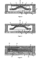
- the electromechanical micro-capacitor with variable capacity represented in Figures 1 to 3 comprises a beam 1 having two ends 2 integral with a ring 3 fixed to a substrate 4 by means of two bases 5 fixing.
- the ring 3 constitutes, thus, a support S for the beam 1.
- the mounting bases 5 are arranged on either side of the ring 3, on an attachment axis AA passing through the center P of the ring 3.
- the beam 1 is disposed on a diameter of the ring 3 perpendicular to the fastening axis AA defined by the fixing bases 5.
- the beam 1 is arranged along an axis BB.
- the micro-capacitor comprises a first electrode 6 integral with the beam 1 and two second electrodes 7, not shown in FIGS. Figures 1 and 2 for the sake of clarity.
- a dotted surface 1a represents a lower face of the beam 1.
- the micro-capacitor comprises an additional support 8 attached to the substrate 4 by means of two additional bases 9.
- the second electrodes 7 are integral with the additional support 8 and the beam 1 is disposed between the substrate 4 and the second electrodes 7.
- Residual stresses due to the fixing of the ring 3 on the substrate 4 cause a buckling of the beam 1, so that the arrow 10 of the beam 1 is close to the second electrodes 7.
- the buckling occurs especially when the ring 3 is constituted by at least one layer under tensile stress along the axis of attachment AA or when it comprises at least one such layer.
- the tensile stress of the ring 3 along the axis fixing AA causes a narrowing of the ring 3 according to the diameter of the ring 3 perpendicular to the fastening axis AA, and then results in a compressive stress of the beam 1 along its longitudinal axis.
- the beam 1 preferably comprises an upper insulating layer 11 arranged opposite the second electrodes 7.
- the arrow 10 of the beam 1 can be in contact with the second electrode 7 without creating an electrical contact between the first electrode 6 and the second electrodes 7.
- an insulating layer may be deposited on the second electrodes 7, facing the first electrode 6.
- the figure 3 represents the micro-capacitor in a rest position, that is to say when the actuation voltage is zero.
- the micro-capacitor according to the invention makes it possible, according to an actuating voltage, to draw the beam 1 further towards the second electrode.
- an increasingly larger portion of the first electrode 6 approaches the second electrode 7, as shown in FIG. figure 4 , and the capacity of the capacitor is greatly increased.
- the micro-capacitor has the advantage that, in its rest position ( figure 3 ), a central portion of the first electrode 6 is automatically close to the second electrodes 7 and, thus, the electrostatic forces are important locally, even by applying a low voltage. These local electrostatic forces make it possible, in particular, to propagate the attraction between the electrodes step by step along the electrodes 6 and 7 and thus to enlarge the zone of contact between the beam 1 and the second electrodes 7.
- the two second electrodes 7 are arranged facing the beam 1, along an axis parallel to the longitudinal axis of the beam 1, respectively on either side of the boom 10 of the beam 1.
- the second electrodes 7 are not arranged opposite the arrow 10 itself, which reduces the capacity of the capacitor in the rest position of the beam 1 and thus expand the range of capacitance variation.
- a method of manufacturing the micro-capacitor according to the invention comprises the deposition under stress of the beam 1 and / or the support S of the beam, so that residual stresses cause a buckling of the beam 1.
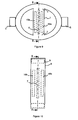
- the beam 1 and the ring 3 can be made in a single stack of layers on a first sacrificial layer 14, as shown in FIG. figure 5 .
- Said stack comprises a lower insulating layer 12, a conductive layer 13 constituting the first electrode 6 and the upper insulating layer 11.
- the conductive layer 13 may be limited to the portion of the stack corresponding to the beam 1, as shown in FIG. figure 5 .
- the ring 3 consists solely of the lower and upper insulating layers 12 and 11.
- the deposition of the lower insulating layer 12 is performed on a first sacrificial layer 14.
- a second sacrificial layer 15 makes it possible to produce the additional support 8.
- the stack constituting the beam 1 and the ring 3 is deposited so that, after removal of the first and second sacrificial layers 14 and 15, the stack is under tensile stress along the axis of attachment AA.
- the tensile stress of the ring 3 causes a stretching of the ring along the axis of attachment AA and, thus, the buckling of the beam 1 along its longitudinal axis.
- the beam itself comprises at least one layer under compressive stress along a longitudinal axis CC of the beam 1.
- the support S is simply constituted by two attachment bases.
- the beam 1 can be made by deposition, on an assembly formed by a first sacrificial layer 14 and the two bases constituting the support S.
- residual stresses due to the attachment of the beam 1 on the mounting bases (S) cause the beam 1 to buckle, so that the arrow 10 of the beam 1 is close to the second electrode 7, after removal of the first sacrificial layer 14, as shown in FIG. figure 8 .
- the residual stresses can be controlled by playing for example on the thicknesses, the dimensions, the geometry and the materials (modulus of Young, Poisson's ratio) of the deposited layers.
- nitride compounds under tensile stress having a thickness of between 0.5 and 1 micron for the ring 3 are used.
- the level of the tensile stress necessary for the boom 10 of the beam 1 to be close of the second electrode 7, can be studied by finite element simulations by varying the values of the stresses to calculate the buckling of the beam 1.
- the value of the stress for which the buckling has an amplitude such that the one-touch beam at one point the second electrode 7.
- the above parameters can also be empirically determined by testing and / or adjusting the nitride deposition parameters, for example the temperature or the deposition power.
- the first electrode 6, which is mobile, may be titanium nitride TiN or gold.
- the thickness of the first electrode 6 is, for example, between 0.3 and 0.4 microns.
- the ring 3 has, for example, an inner diameter of 400 microns and an outer diameter of 450 microns.
- the beam 1 therefore has a length of 400 microns and may, for example, have a width of 60 microns.
- the buckling is, for example, such that the boom 10 of the beam 1 is raised by 12 microns.
- Actuation of the micro-capacitor may be effected through the first and second electrodes.
- the electrical operating voltage is applied between the first electrode 6 and the second electrodes 7, that is to say that the operating voltage is identical to the voltage across the terminals of the micro-capacitor, the capacitance of which varies as a function of the voltage applied to its terminals.
- additional electrodes may be used for actuation.
- additional first and second electrodes for the electrostatic actuation and to completely dissociate the actuation of the first (6) and second (7) electrodes of the micro-capacitor.
- the micro-capacitor comprises at least one additional electrode 16a integral with the beam 1.
- the electrical actuation voltage is thus applied between the additional electrode 16a and the second electrodes 7.
- two additional electrodes 16a integral with the beam 1 can be arranged on either side of the axis BB which is the axis longitudinal beam 1.
- the width of the second electrodes 7 is adapted to the width of the set of two additional electrodes 16a and the first electrode 6.
- the micro-capacitor comprises an additional electrode 16b integral with the additional support 8.
- the electrical actuation voltage is thus applied between the additional electrode 16b and the first electrode 6.
- two additional electrodes 16b integral with the additional support 8 may, for example, be disposed on either side of a longitudinal axis of the additional support 8.
- the two additional electrodes 16b are disposed respectively on either side of the the second single electrode 7 disposed on the axis BB which corresponds to the longitudinal axis of the additional support 8 and the beam 1.
- the width of the first electrode 6 is then adapted to the width of the set of two additional electrodes 16b and the second electrode 7.
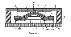
- the beam 1 of the micro-capacitor comprises a layer of piezoelectric material (AIN, PZT, etc.) or thermally expandable material (AI, AISi, Inconel TM, etc.).
- this layer 17 forms, on the lower surface of the beam 1, two distinct zones 17a and 17b respectively disposed at the longitudinal ends of the beam 1.
- two actuating electrodes 18a and 18b partially overlap respectively the zones 17a and 17b of the layer 17.
- the application of an actuating voltage between the electrodes 6 and 18 causes the expansion of the material, piezoelectric or able to deform thermally, of the layer 17.
- the dilation of this material being greater than that of the materials (SiN, oxide, Si, etc.) constituting the structural layers of the beam, there is a bimetallic effect, which causes the appearance of a mechanical torque, thus increasing the bonding zone.
- the length of the layer 17 may be less than or equal to the length L of the beam.
- each zone 17a and 17b has a length substantially close to L / 3.
- the width of the layer 17 is less than or equal to the width of the beam and its thickness is preferably between 0.2 and 1 ⁇ m. This thickness can be calibrated according to the desired displacement.
- first and second electrodes may be arbitrary.
- the micro-capacitor may comprise several first electrodes 6 and / or a single second electrode 7 or more than two second electrodes 7.
Abstract
Description
L'invention concerne un micro-condensateur électromécanique ayant une capacité variable en fonction d'une tension électrique d'actionnement et comportant au moins des première et seconde électrodes, la première électrode étant solidaire d'une poutre ayant deux extrémités solidaires d'un support fixé sur un substrat.The invention relates to an electromechanical micro-capacitor having a variable capacity as a function of an electrical operating voltage and comprising at least first and second electrodes, the first electrode being integral with a beam having two ends integral with a support. fixed on a substrate.
Certains micro-condensateurs électromécaniques à capacité variable ont un fonctionnement basé sur la variation de l'écart entre les deux électrodes du condensateur. Ainsi, la capacité du condensateur est, par exemple, contrôlée par l'actionnement de l'une des électrodes permettant de la rapprocher ou de l'écarter de l'autre électrode. L'actionnement est typiquement réalisé par un actionneur électrostatique. Dans le cas de certains types de micro-condensateurs, les forces électrostatiques entre les électrodes provoquent un brusque collage, ce qui limite la plage de variation de la capacité à une variation de 50%.Some electromechanical micro-capacitors with variable capacitance have an operation based on the variation of the gap between the two electrodes of the capacitor. Thus, the capacity of the capacitor is, for example, controlled by the actuation of one of the electrodes to bring it closer to or away from the other electrode. The actuation is typically performed by an electrostatic actuator. In the case of certain types of micro-capacitors, the electrostatic forces between the electrodes cause abrupt bonding, which limits the range of variation of the capacitance to a variation of 50%.
Le document
L'invention a pour but de remédier à ces inconvénients et, en particulier, un micro-condensateur électromécanique à capacité variable fonctionnant à basse tension électrique d'actionnement et présentant une capacité stable et une grande plage de variation de la capacité.The object of the invention is to overcome these disadvantages and, in particular, a variable capacity electromechanical micro-capacitor operating at low electrical operating voltage and having a stable capacitance and a wide range of capacitance variation.
Selon l'invention, ce but est atteint par les revendications annexées et, plus particulièrement, par le fait que des contraintes résiduelles provoquent un flambement de la poutre, de manière à ce que la flèche de la poutre soit proche de la seconde électrode.According to the invention, this object is achieved by the appended claims and, more particularly, by the fact that residual stresses cause the beam to buckle, so that the deflection of the beam is close to the second electrode.
L'invention a également pour but un procédé de fabrication d'un micro-condensateur selon l'invention, comportant le dépôt sous contrainte d'au moins l'un des éléments choisis parmi la poutre et le support, de manière à ce que des contraintes résiduelles provoquent un flambement de la poutre.The invention also aims at a method of manufacturing a micro-capacitor according to the invention, comprising the deposition under stress of at least one of the elements selected from the beam and the support, so that Residual stresses cause buckling of the beam.
D'autres avantages et caractéristiques ressortiront plus clairement de la description qui va suivre de modes particuliers de réalisation de l'invention donnés à titre d'exemples non limitatifs et représentés aux dessins annexés, dans lesquels :
- La
figure 1 représente, en vue de dessus, un mode de réalisation particulier d'un micro-condensateur selon l'invention. - Les
figures 2 et3 représentent, respectivement en coupe selon l'axe A-A et selon l'axe B-B, le micro-condensateur selon lafigure 1 . - La
figure 4 illustre, en coupe selon l'axe B-B, le fonctionnement du micro-condensateur selon lafigure 1 . - La
figure 5 représente, en coupe selon l'axe B-B, une étape d'un mode de réalisation particulier d'un procédé de fabrication d'un micro-condensateur selon lafigure 1 . - La
figure 6 représente, en vue de dessus, un autre mode de réalisation particulier d'un micro-condensateur selon l'invention. - Les
figures 7 et 8 représentent, en coupe selon l'axe C-C, deux étapes d'un mode de réalisation particulier d'un procédé de fabrication d'un micro-condensateur selon lafigure 6 . - Les
figures 9 et 10 illustrent schématiquement, en vue de dessus, deux modes de réalisation particuliers des électrodes supplémentaires d'un micro-condensateur selon l'invention. - La
figure 11 représente, en coupe selon B-B, une variante de réalisation du micro-condensateur selon lafigure 1 .
- The
figure 1 represents, in top view, a particular embodiment of a micro-capacitor according to the invention. - The
figures 2 and3 represent, respectively in section along the axis AA and along the axis BB, the micro-capacitor according to thefigure 1 . - The
figure 4 illustrates, in section along the axis BB, the operation of the micro-capacitor according to thefigure 1 . - The
figure 5 represents, in section along the axis BB, a step of a particular embodiment of a method of manufacturing a micro-capacitor according to thefigure 1 . - The
figure 6 represents, in top view, another particular embodiment of a micro-capacitor according to the invention. - The
Figures 7 and 8 represent, in section along the axis CC, two steps of a particular embodiment of a method of manufacturing a micro-capacitor according to thefigure 6 . - The
Figures 9 and 10 schematically illustrate, in top view, two particular embodiments of the additional electrodes of a micro-capacitor according to the invention. - The
figure 11 represents, in section along BB, an alternative embodiment of the micro-capacitor according to thefigure 1 .
Le micro-condensateur électromécanique à capacité variable représenté aux
Sur la
Dans le mode de réalisation particulier représenté aux
Des contraintes résiduelles dues à la fixation de l'anneau 3 sur le substrat 4 provoquent un flambement de la poutre 1, de manière à ce que la flèche 10 de la poutre 1 soit proche des secondes électrodes 7. Le flambement se produit notamment lorsque l'anneau 3 est constitué par au moins une couche sous contrainte en traction selon l'axe de fixation A-A ou lorsqu'il comporte au moins une telle couche. La contrainte en traction de l'anneau 3 selon l'axe de fixation A-A provoque un rétrécissement de l'anneau 3 selon le diamètre de l'anneau 3 perpendiculaire à l'axe de fixation A-A, et se traduit alors par une contrainte en compression de la poutre 1 selon son axe longitudinal.Residual stresses due to the fixing of the
Comme représenté à la
La
Le micro-condensateur présente l'avantage que, dans sa position de repos (
Sur la
Un procédé de fabrication du micro-condensateur selon l'invention comporte le dépôt sous contrainte de la poutre 1 et/ou du support S de la poutre, de manière à ce que des contraintes résiduelles provoquent un flambement de la poutre 1. Par exemple, la poutre 1 et l'anneau 3 peuvent être réalisés en un seul empilement de couches sur une première couche sacrificielle 14, comme représenté à la
Dans le mode de réalisation particulier représenté à la
L'empilement constituant la poutre 1 et l'anneau 3 est déposé de manière à ce que, après enlèvement des première et seconde couches sacrificielles 14 et 15, l'empilement soit sous contrainte en traction selon l'axe de fixation A-A. Ainsi, la contrainte en traction de l'anneau 3 provoque un étirement de l'anneau selon l'axe de fixation A-A et, ainsi, le flambement de la poutre 1 selon son axe longitudinal.The stack constituting the
Dans un autre mode de réalisation particulier représenté aux
Les contraintes résiduelles peuvent être maîtrisées en jouant par exemple sur les épaisseurs, les dimensions, la géométrie et les matériaux (module de Young, coefficient de Poisson) des couches déposées. On utilise, par exemple, des composés nitrurés sous contrainte en traction ayant une épaisseur comprise entre 0,5 et 1 micron pour l'anneau 3. Le niveau de la contrainte en traction, nécessaire pour que la flèche 10 de la poutre 1 soit proche de la seconde électrode 7, peut être étudié par des simulations par éléments finis en faisant varier les valeurs des contraintes pour calculer le flambement de la poutre 1. Ainsi, on détermine la valeur de la contrainte pour laquelle le flambement présente une amplitude telle que la poutre 1 touche en un point la seconde électrode 7.The residual stresses can be controlled by playing for example on the thicknesses, the dimensions, the geometry and the materials (modulus of Young, Poisson's ratio) of the deposited layers. For example, nitride compounds under tensile stress having a thickness of between 0.5 and 1 micron for the
On peut également déterminer empiriquement les paramètres ci-dessus par des essais et/ou ajuster les paramètres de dépôt du nitrure, par exemple la température ou la puissance de dépôt. La première électrode 6, qui est mobile, peut être en nitrure de titane TiN ou de l'or. L'épaisseur de la première électrode 6 est, par exemple, comprise entre 0,3 et 0,4 microns.The above parameters can also be empirically determined by testing and / or adjusting the nitride deposition parameters, for example the temperature or the deposition power. The
L'anneau 3 a, par exemple, un diamètre intérieur de 400 microns et un diamètre extérieur de 450 microns. La poutre 1 a donc une longueur de 400 microns et peut, par exemple, avoir une largeur de 60 microns. Le flambement est, par exemple, tel que la flèche 10 de la poutre 1 est surélevée de 12 microns.The
L'actionnement du micro-condensateur peut être effectué par l'intermédiaire des première et seconde électrodes. Ainsi, la tension électrique d'actionnement est appliquée entre la première électrode 6 et les secondes électrodes 7, c'est-à-dire que la tension d'actionnement est identique à la tension aux bornes du micro-condensateur, dont la capacité varie ainsi en fonction de la tension appliquée à ses bornes.Actuation of the micro-capacitor may be effected through the first and second electrodes. Thus, the electrical operating voltage is applied between the
Pour des applications radiofréquence, il est avantageux de dissocier les bornes du micro-condensateur et les électrodes d'actionnement, de manière à séparer la zone d'actionnement de la zone active définissant la valeur de la capacité variable. En effet, un signal radiofréquence de forte puissance superposé à la tension d'actionnement pourrait perturber le fonctionnement du micro-condensateur. Dans ce cas, des électrodes supplémentaires peuvent être utilisées pour l'actionnement. On peut, par exemple, utiliser des premières et secondes électrodes supplémentaires pour l'actionnement électrostatique et dissocier complètement l'actionnement des première (6) et seconde (7) électrodes du micro-condensateur.For radiofrequency applications, it is advantageous to dissociate the terminals of the micro-capacitor and the actuation electrodes, so as to separate the actuation zone from the active zone defining the value of the variable capacitance. Indeed, a high power radiofrequency signal superimposed on the actuating voltage could disturb the operation of the micro-capacitor. In this case, additional electrodes may be used for actuation. For example, it is possible to use additional first and second electrodes for the electrostatic actuation and to completely dissociate the actuation of the first (6) and second (7) electrodes of the micro-capacitor.
Il est également possible d'utiliser l'une des première et seconde électrodes pour l'actionnement. Par exemple, le micro-condensateur comporte au moins une électrode supplémentaire 16a solidaire de la poutre 1. La tension électrique d'actionnement est ainsi appliquée entre l'électrode supplémentaire 16a et les secondes électrodes 7. Comme représenté à la
Dans un autre mode de réalisation particulier de l'actionnement, le micro-condensateur comporte une électrode supplémentaire 16b solidaire du support supplémentaire 8. La tension électrique d'actionnement est ainsi appliquée entre l'électrode supplémentaire 16b et la première électrode 6. Comme représenté à la
Dans une variante de réalisation, la poutre 1 du micro-condensateur comporte une couche en matériau piézoélectrique (AIN, PZT,etc.) ou en matériau apte à se dilater thermiquement (AI, AISi, Inconel™, etc.). Dans le mode de réalisation particulier illustré à la
La longueur de la couche 17 peut être inférieure ou égale à la longueur L de la poutre. Dans un mode de réalisation préférentiel, chaque zone 17a et 17b a une longueur sensiblement voisine de L/3. La largeur de la couche 17 est inférieure ou égale à la largeur de la poutre et son épaisseur est, de préférence, comprise entre 0,2 et 1 µm. Cette épaisseur peut être calibrée en fonction du déplacement désiré.The length of the layer 17 may be less than or equal to the length L of the beam. In a preferred embodiment, each
L'invention n'est pas limitée aux modes de réalisation représentés. En particulier, le nombre des première et seconde électrodes peut être quelconque. Par exemple, le micro-condensateur peut comporter plusieurs premières électrodes 6 et/ou une seule seconde électrode 7 ou plus de deux secondes électrodes 7.The invention is not limited to the embodiments shown. In particular, the number of first and second electrodes may be arbitrary. For example, the micro-capacitor may comprise several
Claims (16)
- Electromechanical micro-capacitor having a variable capacitance according to an electrical actuating voltage and comprising at least first (6) and second (7) electrodes, the first electrode (6) being integral to a beam (1) having two ends (2) securedly affixed to a support (S) fixed onto a substrate (4), micro-capacitor characterized in that residual stresses cause buckling of the beam (1) so that the arch (10) of the beam (1) is close to the second electrode (7).
- Micro-capacitor according to claim 1, characterized in that the beam (1) comprises an insulating layer (11) arranged facing the second electrode (7).
- Micro-capacitor according to claim 2, characterized in that the arch (10) of the beam (1) is in contact with the second electrode (7).
- Micro-capacitor according to any one of the claims 1 to 3, characterized in that the support (S) is formed by a ring (3) fixed to the substrate (4) by means of two fixing bases (5) arranged on each side of the ring (3) on a fixing axis (A-A) passing through the centre (P) of the ring (3), the beam (1) being arranged on a diameter of the ring (3) perpendicular to the fixing axis (A-A), the ring (3) comprising at least one layer tensile stressed along the fixing axis (A-A).
- Micro-capacitor according to any one of the claims 1 to 4, characterized in that the beam (1) comprises at least one layer stressed in compression along a longitudinal axis (B-B) of the beam (1).
- Micro-capacitor according to any one of the claims 1 to 5, characterized in that the second electrode (7) is integral to an additional support (8), the beam (1) being arranged between the substrate (4) and the second electrode (7).
- Micro-capacitor according to claim 6, characterized in that two second electrodes (7) are arranged facing the beam (1) along an axis parallel to the longitudinal axis of the beam (1), respectively on each side of the arch (10) of the beam (1).
- Micro-capacitor according to any one of the claims 1 to 7, characterized in that the first (6) and second (7) electrodes constitute electrical actuating means, the electrical actuating voltage being designed to be applied between the first (6) and second (7) electrodes.
- Micro-capacitor according to any one of the claims 1 to 7, characterized in that the beam (1) comprises a layer (17) made of a material chosen from piezoelectric materials and thermally deformable materials and at least partially covered by an actuating electrode (18), the electrical actuating voltage being designed to be applied between the actuating electrode (18) and the first electrode (6).
- Micro-capacitor according to any one of the claims 1 to 7, characterized in that it comprises electrical actuating means comprising at least one additional electrode (16a) integral to the beam (1), the electrical actuating voltage being designed to be applied between the additional electrode (16a) and the second electrode (7).
- Micro-capacitor according to claim 10, characterized in that the two additional electrodes (16a) integral to the beam (1) are arranged on each side of a longitudinal axis of the beam (1).
- Micro-capacitor according to one of the claims 6 and 7, characterized in that it comprises electrical actuating means comprising at least one additional electrode (16b) integral to the additional support (8), the electrical actuating voltage being designed to be applied between the additional electrode (16b) and the first electrode (6).
- Micro-capacitor according to claim 12, characterized in that two additional electrodes (16b) integral to the additional support (8) are arranged on each side of a longitudinal axis of the additional support (8).
- Method for producing an electromechanical micro-capacitor according to any one of the claims 1 to 13, characterized in that it comprises stressed deposition of at least one of the elements chosen from the beam (1) and the support (S), so that residual stress cause buckling of the beam (1).
- Method according to claim 14, characterized in that it comprises fabrication of the beam (1) and the ring (3) in a single stacking of layers on a sacrificial layer (14), so that, after the sacrificial layer (14) has been removed, the ring (3) is tensile stressed along the fixing axis (A-A).
- Method according to claim 14, characterized in that it comprises fabrication of the beam (1), on an assembly formed by a sacrificial layer (14) and the support (S), by deposition of at least one layer stressed in compression along a longitudinal axis (B-B) of the beam (1).
Applications Claiming Priority (1)
| Application Number | Priority Date | Filing Date | Title |
|---|---|---|---|
| FR0504105A FR2884960B1 (en) | 2005-04-25 | 2005-04-25 | ELECTROMECHANICAL MICRO-CAPACITOR WITH VARIABLE CAPACITY AND METHOD OF MANUFACTURING SUCH MICRO-CAPACITOR |
Publications (2)
| Publication Number | Publication Date |
|---|---|
| EP1717830A1 EP1717830A1 (en) | 2006-11-02 |
| EP1717830B1 true EP1717830B1 (en) | 2010-06-09 |
Family
ID=34955194
Family Applications (1)
| Application Number | Title | Priority Date | Filing Date |
|---|---|---|---|
| EP06354011A Active EP1717830B1 (en) | 2005-04-25 | 2006-03-20 | Electromechanical micro-capacitor with variable capacity and process of manufacture of such a capacitor |
Country Status (6)
| Country | Link |
|---|---|
| US (1) | US7558046B2 (en) |
| EP (1) | EP1717830B1 (en) |
| JP (1) | JP2006310854A (en) |
| AT (1) | ATE470942T1 (en) |
| DE (1) | DE602006014759D1 (en) |
| FR (1) | FR2884960B1 (en) |
Cited By (2)
| Publication number | Priority date | Publication date | Assignee | Title |
|---|---|---|---|---|
| US10332687B2 (en) | 2017-10-23 | 2019-06-25 | Blackberry Limited | Tunable coplanar capacitor with vertical tuning and lateral RF path and methods for manufacturing thereof |
| US10497774B2 (en) | 2017-10-23 | 2019-12-03 | Blackberry Limited | Small-gap coplanar tunable capacitors and methods for manufacturing thereof |
Families Citing this family (3)
| Publication number | Priority date | Publication date | Assignee | Title |
|---|---|---|---|---|
| DE102008007034A1 (en) * | 2008-01-31 | 2009-08-13 | Siemens Aktiengesellschaft | Capacitor capacitance capacitor assembly, method of fabricating the capacitor assembly, and use of the capacitor assembly |
| JP5644938B2 (en) * | 2011-03-29 | 2014-12-24 | 富士通株式会社 | Electronic device and manufacturing method thereof |
| US11431046B2 (en) | 2018-08-21 | 2022-08-30 | Nio Technology (Anhui) Co., Ltd. | Lithium-ion cell using aluminum can |
Family Cites Families (12)
| Publication number | Priority date | Publication date | Assignee | Title |
|---|---|---|---|---|
| JPH08213282A (en) * | 1995-02-01 | 1996-08-20 | Murata Mfg Co Ltd | Variable capacitance capacitor |
| US6034414A (en) * | 1997-11-18 | 2000-03-07 | Industrial Technology Research Institute | Variable capacitor using resistor generated heat to control dielectric thickness |
| US6496351B2 (en) * | 1999-12-15 | 2002-12-17 | Jds Uniphase Inc. | MEMS device members having portions that contact a substrate and associated methods of operating |
| US6396677B1 (en) * | 2000-05-17 | 2002-05-28 | Xerox Corporation | Photolithographically-patterned variable capacitor structures and method of making |
| US6625004B1 (en) * | 2001-08-31 | 2003-09-23 | Superconductor Technologies, Inc. | Electrostatic actuators with intrinsic stress gradient |
| FR2831705B1 (en) * | 2001-10-25 | 2004-08-27 | Commissariat Energie Atomique | HIGH RATIO VARIABLE MICRO-CAPACITOR AND LOW ACTUATION VOLTAGE |
| JP4151338B2 (en) * | 2002-07-30 | 2008-09-17 | 松下電器産業株式会社 | Variable capacitance element and method for forming the same |
| JP2004172504A (en) * | 2002-11-21 | 2004-06-17 | Fujitsu Media Device Kk | Variable capacitor, package provided therewith, and method for manufacturing the same |
| JP2004221128A (en) * | 2003-01-09 | 2004-08-05 | Murata Mfg Co Ltd | Variable capacitor |
| WO2005001863A1 (en) * | 2003-06-02 | 2005-01-06 | Carnegie Mellon University | Self-assembling mems devices having thermal actuation |
| WO2005027257A1 (en) * | 2003-09-08 | 2005-03-24 | Murata Manufacturing Co., Ltd. | Variable capacitance element |
| JP2006210843A (en) * | 2005-01-31 | 2006-08-10 | Fujitsu Ltd | Variable capacitor and manufacturing method thereof |
-
2005
- 2005-04-25 FR FR0504105A patent/FR2884960B1/en not_active Expired - Fee Related
-
2006
- 2006-03-20 EP EP06354011A patent/EP1717830B1/en active Active
- 2006-03-20 AT AT06354011T patent/ATE470942T1/en not_active IP Right Cessation
- 2006-03-20 DE DE602006014759T patent/DE602006014759D1/en active Active
- 2006-03-29 US US11/391,555 patent/US7558046B2/en active Active
- 2006-04-25 JP JP2006120375A patent/JP2006310854A/en active Pending
Cited By (4)
| Publication number | Priority date | Publication date | Assignee | Title |
|---|---|---|---|---|
| US10332687B2 (en) | 2017-10-23 | 2019-06-25 | Blackberry Limited | Tunable coplanar capacitor with vertical tuning and lateral RF path and methods for manufacturing thereof |
| US10497774B2 (en) | 2017-10-23 | 2019-12-03 | Blackberry Limited | Small-gap coplanar tunable capacitors and methods for manufacturing thereof |
| US10770540B2 (en) | 2017-10-23 | 2020-09-08 | Nxp Usa, Inc. | Small-gap coplanar tunable capacitors and methods for manufacturing thereof |
| US10825612B2 (en) | 2017-10-23 | 2020-11-03 | Nxp Usa, Inc. | Tunable coplanar capacitor with vertical tuning and lateral RF path and methods for manufacturing thereof |
Also Published As
| Publication number | Publication date |
|---|---|
| US7558046B2 (en) | 2009-07-07 |
| ATE470942T1 (en) | 2010-06-15 |
| EP1717830A1 (en) | 2006-11-02 |
| US20060238956A1 (en) | 2006-10-26 |
| JP2006310854A (en) | 2006-11-09 |
| DE602006014759D1 (en) | 2010-07-22 |
| FR2884960B1 (en) | 2007-07-06 |
| FR2884960A1 (en) | 2006-10-27 |
Similar Documents
| Publication | Publication Date | Title |
|---|---|---|
| EP2747452B1 (en) | Membrane device with controlled movement | |
| EP1040492A1 (en) | Microsystem with element deformable by the action of a heat-actuated device | |
| CH691559A5 (en) | magnetic micro-switch and its production process. | |
| EP2663091A1 (en) | Digital speaker with enhanced performance | |
| EP1717830B1 (en) | Electromechanical micro-capacitor with variable capacity and process of manufacture of such a capacitor | |
| WO2003069776A2 (en) | Tunable bulk acoustic wave mems microresonator | |
| EP1743349B1 (en) | Low consumption and low actuation voltage microswitch | |
| EP3514388B1 (en) | Piezoelectric transducer | |
| EP1736435A1 (en) | Electrostatic actuator with a conducting and suspended pivot member | |
| EP2309559A1 (en) | Piezoelectric actuating structure comprising an integrated piezoresistive strain gauge and manufacturing method thereof | |
| EP2267893B1 (en) | Bulk acoustic wave resonator with partially filled cavities | |
| EP1458095B1 (en) | Method of manufacturing a piezoelectric tunable microresonator | |
| EP1438728B1 (en) | Micro electro mechanical systems (mems) with variable high-ratio and low-voltage actuation micro-capacitor | |
| CA2555806C (en) | Bimorph mirror provided with two piezoelectric layers separated by a central core made of a semi-rigid material | |
| EP3828943B1 (en) | Mechanical microsystem and corresponding production process | |
| EP0874379B1 (en) | Magnetic microswitch and method of making | |
| EP1009040B1 (en) | Actuators of active piezoelectric or electrostrictive material | |
| EP1846320B1 (en) | Micromechanical device comprising a mobile beam | |
| EP3663733A1 (en) | Heat detector with suspended membrane comprising a deformable thermal short-circuit part | |
| EP1224718B1 (en) | Tuneable active microcavity and related method for making same | |
| EP1805100A1 (en) | Microsystem comprising a deformable bridge | |
| EP2673816B1 (en) | Microelectromechanical device with piezoelectric actuation structure | |
| EP3671873B1 (en) | Electromechanical microsystem comprising an active element provided with a structured core layer | |
| EP2603448B1 (en) | Microelectromechanical system with air gap | |
| EP0441269B1 (en) | Electrostatic micromotor |
Legal Events
| Date | Code | Title | Description |
|---|---|---|---|
| PUAI | Public reference made under article 153(3) epc to a published international application that has entered the european phase |
Free format text: ORIGINAL CODE: 0009012 |
|
| AK | Designated contracting states |
Kind code of ref document: A1 Designated state(s): AT BE BG CH CY CZ DE DK EE ES FI FR GB GR HU IE IS IT LI LT LU LV MC NL PL PT RO SE SI SK TR |
|
| AX | Request for extension of the european patent |
Extension state: AL BA HR MK YU |
|
| 17P | Request for examination filed |
Effective date: 20070512 |
|
| AKX | Designation fees paid |
Designated state(s): AT BE BG CH CY CZ DE DK EE ES FI FR GB GR HU IE IS IT LI LT LU LV MC NL PL PT RO SE SI SK TR |
|
| GRAP | Despatch of communication of intention to grant a patent |
Free format text: ORIGINAL CODE: EPIDOSNIGR1 |
|
| GRAS | Grant fee paid |
Free format text: ORIGINAL CODE: EPIDOSNIGR3 |
|
| GRAA | (expected) grant |
Free format text: ORIGINAL CODE: 0009210 |
|
| AK | Designated contracting states |
Kind code of ref document: B1 Designated state(s): AT BE BG CH CY CZ DE DK EE ES FI FR GB GR HU IE IS IT LI LT LU LV MC NL PL PT RO SE SI SK TR |
|
| REG | Reference to a national code |
Ref country code: CH Ref legal event code: EP |
|
| RAP2 | Party data changed (patent owner data changed or rights of a patent transferred) |
Owner name: COMMISSARIAT A L'ENERGIE ATOMIQUE ET AUX ENERGIES |
|
| REG | Reference to a national code |
Ref country code: IE Ref legal event code: FG4D Free format text: LANGUAGE OF EP DOCUMENT: FRENCH |
|
| REF | Corresponds to: |
Ref document number: 602006014759 Country of ref document: DE Date of ref document: 20100722 Kind code of ref document: P |
|
| REG | Reference to a national code |
Ref country code: NL Ref legal event code: VDEP Effective date: 20100609 |
|
| PG25 | Lapsed in a contracting state [announced via postgrant information from national office to epo] |
Ref country code: SE Free format text: LAPSE BECAUSE OF FAILURE TO SUBMIT A TRANSLATION OF THE DESCRIPTION OR TO PAY THE FEE WITHIN THE PRESCRIBED TIME-LIMIT Effective date: 20100609 Ref country code: LT Free format text: LAPSE BECAUSE OF FAILURE TO SUBMIT A TRANSLATION OF THE DESCRIPTION OR TO PAY THE FEE WITHIN THE PRESCRIBED TIME-LIMIT Effective date: 20100609 |
|
| LTIE | Lt: invalidation of european patent or patent extension |
Effective date: 20100609 |
|
| PG25 | Lapsed in a contracting state [announced via postgrant information from national office to epo] |
Ref country code: FI Free format text: LAPSE BECAUSE OF FAILURE TO SUBMIT A TRANSLATION OF THE DESCRIPTION OR TO PAY THE FEE WITHIN THE PRESCRIBED TIME-LIMIT Effective date: 20100609 Ref country code: AT Free format text: LAPSE BECAUSE OF FAILURE TO SUBMIT A TRANSLATION OF THE DESCRIPTION OR TO PAY THE FEE WITHIN THE PRESCRIBED TIME-LIMIT Effective date: 20100609 Ref country code: SI Free format text: LAPSE BECAUSE OF FAILURE TO SUBMIT A TRANSLATION OF THE DESCRIPTION OR TO PAY THE FEE WITHIN THE PRESCRIBED TIME-LIMIT Effective date: 20100609 Ref country code: LV Free format text: LAPSE BECAUSE OF FAILURE TO SUBMIT A TRANSLATION OF THE DESCRIPTION OR TO PAY THE FEE WITHIN THE PRESCRIBED TIME-LIMIT Effective date: 20100609 |
|
| PG25 | Lapsed in a contracting state [announced via postgrant information from national office to epo] |
Ref country code: PL Free format text: LAPSE BECAUSE OF FAILURE TO SUBMIT A TRANSLATION OF THE DESCRIPTION OR TO PAY THE FEE WITHIN THE PRESCRIBED TIME-LIMIT Effective date: 20100609 Ref country code: GR Free format text: LAPSE BECAUSE OF FAILURE TO SUBMIT A TRANSLATION OF THE DESCRIPTION OR TO PAY THE FEE WITHIN THE PRESCRIBED TIME-LIMIT Effective date: 20100910 Ref country code: CY Free format text: LAPSE BECAUSE OF FAILURE TO SUBMIT A TRANSLATION OF THE DESCRIPTION OR TO PAY THE FEE WITHIN THE PRESCRIBED TIME-LIMIT Effective date: 20100609 |
|
| REG | Reference to a national code |
Ref country code: IE Ref legal event code: FD4D |
|
| PG25 | Lapsed in a contracting state [announced via postgrant information from national office to epo] |
Ref country code: NL Free format text: LAPSE BECAUSE OF FAILURE TO SUBMIT A TRANSLATION OF THE DESCRIPTION OR TO PAY THE FEE WITHIN THE PRESCRIBED TIME-LIMIT Effective date: 20100609 Ref country code: IE Free format text: LAPSE BECAUSE OF FAILURE TO SUBMIT A TRANSLATION OF THE DESCRIPTION OR TO PAY THE FEE WITHIN THE PRESCRIBED TIME-LIMIT Effective date: 20100609 Ref country code: EE Free format text: LAPSE BECAUSE OF FAILURE TO SUBMIT A TRANSLATION OF THE DESCRIPTION OR TO PAY THE FEE WITHIN THE PRESCRIBED TIME-LIMIT Effective date: 20100609 |
|
| PG25 | Lapsed in a contracting state [announced via postgrant information from national office to epo] |
Ref country code: RO Free format text: LAPSE BECAUSE OF FAILURE TO SUBMIT A TRANSLATION OF THE DESCRIPTION OR TO PAY THE FEE WITHIN THE PRESCRIBED TIME-LIMIT Effective date: 20100609 Ref country code: CZ Free format text: LAPSE BECAUSE OF FAILURE TO SUBMIT A TRANSLATION OF THE DESCRIPTION OR TO PAY THE FEE WITHIN THE PRESCRIBED TIME-LIMIT Effective date: 20100609 Ref country code: IS Free format text: LAPSE BECAUSE OF FAILURE TO SUBMIT A TRANSLATION OF THE DESCRIPTION OR TO PAY THE FEE WITHIN THE PRESCRIBED TIME-LIMIT Effective date: 20101009 Ref country code: PT Free format text: LAPSE BECAUSE OF FAILURE TO SUBMIT A TRANSLATION OF THE DESCRIPTION OR TO PAY THE FEE WITHIN THE PRESCRIBED TIME-LIMIT Effective date: 20101011 Ref country code: SK Free format text: LAPSE BECAUSE OF FAILURE TO SUBMIT A TRANSLATION OF THE DESCRIPTION OR TO PAY THE FEE WITHIN THE PRESCRIBED TIME-LIMIT Effective date: 20100609 |
|
| PLBE | No opposition filed within time limit |
Free format text: ORIGINAL CODE: 0009261 |
|
| STAA | Information on the status of an ep patent application or granted ep patent |
Free format text: STATUS: NO OPPOSITION FILED WITHIN TIME LIMIT |
|
| PG25 | Lapsed in a contracting state [announced via postgrant information from national office to epo] |
Ref country code: DK Free format text: LAPSE BECAUSE OF FAILURE TO SUBMIT A TRANSLATION OF THE DESCRIPTION OR TO PAY THE FEE WITHIN THE PRESCRIBED TIME-LIMIT Effective date: 20100609 |
|
| 26N | No opposition filed |
Effective date: 20110310 |
|
| REG | Reference to a national code |
Ref country code: DE Ref legal event code: R097 Ref document number: 602006014759 Country of ref document: DE Effective date: 20110309 |
|
| BERE | Be: lapsed |
Owner name: COMMISSARIAT A L'ENERGIE ATOMIQUE Effective date: 20110331 |
|
| PG25 | Lapsed in a contracting state [announced via postgrant information from national office to epo] |
Ref country code: MC Free format text: LAPSE BECAUSE OF NON-PAYMENT OF DUE FEES Effective date: 20110331 |
|
| REG | Reference to a national code |
Ref country code: CH Ref legal event code: PL |
|
| PG25 | Lapsed in a contracting state [announced via postgrant information from national office to epo] |
Ref country code: BE Free format text: LAPSE BECAUSE OF NON-PAYMENT OF DUE FEES Effective date: 20110331 |
|
| PG25 | Lapsed in a contracting state [announced via postgrant information from national office to epo] |
Ref country code: CH Free format text: LAPSE BECAUSE OF NON-PAYMENT OF DUE FEES Effective date: 20110331 Ref country code: LI Free format text: LAPSE BECAUSE OF NON-PAYMENT OF DUE FEES Effective date: 20110331 |
|
| PGFP | Annual fee paid to national office [announced via postgrant information from national office to epo] |
Ref country code: IT Payment date: 20120328 Year of fee payment: 7 |
|
| PG25 | Lapsed in a contracting state [announced via postgrant information from national office to epo] |
Ref country code: LU Free format text: LAPSE BECAUSE OF NON-PAYMENT OF DUE FEES Effective date: 20110320 |
|
| PG25 | Lapsed in a contracting state [announced via postgrant information from national office to epo] |
Ref country code: TR Free format text: LAPSE BECAUSE OF FAILURE TO SUBMIT A TRANSLATION OF THE DESCRIPTION OR TO PAY THE FEE WITHIN THE PRESCRIBED TIME-LIMIT Effective date: 20100609 Ref country code: BG Free format text: LAPSE BECAUSE OF FAILURE TO SUBMIT A TRANSLATION OF THE DESCRIPTION OR TO PAY THE FEE WITHIN THE PRESCRIBED TIME-LIMIT Effective date: 20100909 |
|
| PG25 | Lapsed in a contracting state [announced via postgrant information from national office to epo] |
Ref country code: ES Free format text: LAPSE BECAUSE OF FAILURE TO SUBMIT A TRANSLATION OF THE DESCRIPTION OR TO PAY THE FEE WITHIN THE PRESCRIBED TIME-LIMIT Effective date: 20100920 Ref country code: HU Free format text: LAPSE BECAUSE OF FAILURE TO SUBMIT A TRANSLATION OF THE DESCRIPTION OR TO PAY THE FEE WITHIN THE PRESCRIBED TIME-LIMIT Effective date: 20100609 |
|
| PG25 | Lapsed in a contracting state [announced via postgrant information from national office to epo] |
Ref country code: IT Free format text: LAPSE BECAUSE OF NON-PAYMENT OF DUE FEES Effective date: 20130320 |
|
| REG | Reference to a national code |
Ref country code: FR Ref legal event code: PLFP Year of fee payment: 11 |
|
| REG | Reference to a national code |
Ref country code: FR Ref legal event code: PLFP Year of fee payment: 12 |
|
| REG | Reference to a national code |
Ref country code: FR Ref legal event code: PLFP Year of fee payment: 13 |
|
| PGFP | Annual fee paid to national office [announced via postgrant information from national office to epo] |
Ref country code: FR Payment date: 20230321 Year of fee payment: 18 |
|
| PGFP | Annual fee paid to national office [announced via postgrant information from national office to epo] |
Ref country code: GB Payment date: 20230321 Year of fee payment: 18 Ref country code: DE Payment date: 20230320 Year of fee payment: 18 |