EP1692831B1 - Power savings in serial link transmitters - Google Patents
Power savings in serial link transmitters Download PDFInfo
- Publication number
- EP1692831B1 EP1692831B1 EP04791261A EP04791261A EP1692831B1 EP 1692831 B1 EP1692831 B1 EP 1692831B1 EP 04791261 A EP04791261 A EP 04791261A EP 04791261 A EP04791261 A EP 04791261A EP 1692831 B1 EP1692831 B1 EP 1692831B1
- Authority
- EP
- European Patent Office
- Prior art keywords
- segment
- data
- segments
- output
- circuit
- Prior art date
- Legal status (The legal status is an assumption and is not a legal conclusion. Google has not performed a legal analysis and makes no representation as to the accuracy of the status listed.)
- Not-in-force
Links
- 230000003111 delayed effect Effects 0.000 claims abstract description 16
- 230000008859 change Effects 0.000 claims abstract description 4
- 238000010586 diagram Methods 0.000 description 8
- 230000005540 biological transmission Effects 0.000 description 5
- 238000004891 communication Methods 0.000 description 4
- 238000013461 design Methods 0.000 description 4
- 230000007704 transition Effects 0.000 description 3
- 238000013459 approach Methods 0.000 description 2
- 238000012986 modification Methods 0.000 description 2
- 230000004048 modification Effects 0.000 description 2
- 230000011664 signaling Effects 0.000 description 2
- 230000003213 activating effect Effects 0.000 description 1
- 230000007423 decrease Effects 0.000 description 1
- 238000012545 processing Methods 0.000 description 1
- 230000004044 response Effects 0.000 description 1
- 230000009466 transformation Effects 0.000 description 1
Images


Classifications
-
- H—ELECTRICITY
- H04—ELECTRIC COMMUNICATION TECHNIQUE
- H04L—TRANSMISSION OF DIGITAL INFORMATION, e.g. TELEGRAPHIC COMMUNICATION
- H04L25/00—Baseband systems
- H04L25/02—Details ; arrangements for supplying electrical power along data transmission lines
- H04L25/0264—Arrangements for coupling to transmission lines
- H04L25/028—Arrangements specific to the transmitter end
-
- H—ELECTRICITY
- H03—ELECTRONIC CIRCUITRY
- H03K—PULSE TECHNIQUE
- H03K17/00—Electronic switching or gating, i.e. not by contact-making and –breaking
- H03K17/16—Modifications for eliminating interference voltages or currents
- H03K17/161—Modifications for eliminating interference voltages or currents in field-effect transistor switches
- H03K17/162—Modifications for eliminating interference voltages or currents in field-effect transistor switches without feedback from the output circuit to the control circuit
- H03K17/163—Soft switching
- H03K17/164—Soft switching using parallel switching arrangements
Definitions
- the present invention relates to power savings in serial link transmitters.
- patent application US 2002/0149402 A1 shows a current mode output driver comprising a plurality of parallel line driver segments which are always enabled and which deliver signals of fixed output power.
- the patent application US 6,288,581 B1 discloses an individual line driver comprising a prebuffer, an output stage, an enable input and an input for boosting the output current immediately after a data transition.
- serializer In order for high-speed serial transmission to occur, the digital data signal from inside the computer must be transformed from the parallel format into a serial format prior to transmission of the data over the serial communication link. This transformation is generally accomplished by processing the computer's internal data signal through, a piece of computer equipment known as a serial link transmitter or "serializer.”
- the function of the serializer is to receive a parallel data stream as input and, by manipulating the parallel data stream, output a serial form of the data capable of high-speed transmission over a suitable communication link.
- a piece of computer equipment known as a "deserializer" is employed to convert the incoming data from the serial format to a parallel format for use within the destination computer system.
- HSS serializer/deserializer
- the ability to adjust the transmitter amplitude is a desirable feature.
- the amount of current steered to the output of a differential transmitter need only be controlled to provide an adjustment to the transmitter amplitude.
- design of the transmitter must take into consideration a maximum current situation and size the transmitter devices accordingly to handle the maximum current case. Unfortunately, such a simple approach causes power to be wasted in lower amplitude situations.
- aspects of saving power in a serial link transmitter include providing a parallel arrangement of segments, each segment comprising prebuffer and output stage circuitry of the serial link transmitter and each segment enabled independently to achieve multiple power levels and multiple levels of pre-emphasis while maintaining a substantially constant propagation delay in a signal path of the serial link transmitter. Further aspects include providing a bypass path in the prebuffer stage circuitry to implement a controllable idle state in the segments and tail current and resistive load elements in the prebuffer circuitry as sectioned portions for slew rate control capability.
- control element with pre-emphasis delay circuitry in the transmitter signal path to allow inversion of a last delayed bit of the pre-emphasis delay circuitry to achieve a polarity change of a pre-emphasis weight.
- a circuit for a serial link transmitter comprising: a data input; a data output; and, a plurality of segments; characterized in that each segment comprises: a segment input connected to the data input; a timing element; a buffer; an output stage having a plurality of current enable inputs for selectively varying output power delivered by the output stage; a segment output connected to the data output; and a segment enable input connected to the timing element, the buffer, and the output stage, for selectively enabling the segment; wherein the segment input is connected to the segment output via the timing element, the buffer and the output stage in series; wherein the data input is connected to one of the segments via a delay to produce a delayed segment; and wherein, while maintaining a constant propagation delay in the transmitter, the amplitude and pre-emphasis of data signals applied to the data input of the circuit are variable at the data output of the circuit, in dependence on a combination of segment enable signals selectively applied to the segment enable inputs of the
- a segmented prebuffer and output stage circuitry implementation of the present invention achieves a noise immune design with scalable power consumption. Further, amplitude levels of the transmitter are adjustable with uniform timing.
- the present invention relates to power savings in serial link transmitters.
- the following description is presented to enable one of ordinary skill in the art to make and use examples of the invention and is provided in the context of a patent application and its requirements.
- Various modifications to the preferred embodiment and the generic principles and features described herein will be readily apparent to those skilled in the art.
- the present invention is not intended to be limited to the embodiment shown but is to be accorded the widest scope consistent with the principles and features described herein.
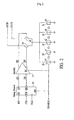
- FIG. 1 a circuit diagram of an example embodiment of a segmented transmitter is presented.
- four different output power levels can be achieved with an adjustable amount of pre-emphasis.
- a differential data input signal, DATA_IN is transmitted via the segments 10 and 12 as a differential data output signal, DATA_OUT, whose amplitude is determined based upon the current transmitted on the output signal linens to the termination resistors 14 and 16.
- the DATA_IN signal is input directly to each of the segments 10 and is delayed via delay element 18 and inverted for input to the segment 12.
- the segments 10 and 12 each comprise an equivalent circuit structure, as described in more detail with reference to Figure 2 .
- the example embodiment includes four (undelayed) segments 10 and one (delayed) segment 12 (i.e., a 4:1 ratio), this is meant as illustrative and not restrictive of the number of segments (or ratio) that can be included.
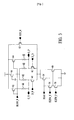
- each segment includes a timing element 20 (e.g., a latch or multiplexer) coupled to a prebuffer 22, where each output (Q_N, Q_P) of the prebuffer 22 is coupled to a transistor 24, 26 from which the output signals OUT_N, OUT_P result. Coupled to transistors 24 and 26 are current sources 28, 30, 32, 34, and 36. The state of the ENABLE signal controls the enabling of the timing element 20, prebuffer 22, and current source 28 (which, for the example, provides one current unit, where one current unit represents e.g., 375 micro amps).
- a timing element 20 e.g., a latch or multiplexer
- each output (Q_N, Q_P) of the prebuffer 22 is coupled to a transistor 24, 26 from which the output signals OUT_N, OUT_P result. Coupled to transistors 24 and 26 are current sources 28, 30, 32, 34, and 36.
- the state of the ENABLE signal controls the enabling of the timing element 20, prebuffer 22, and current source 28
- the state of the control signals input to C0, C1, C2, and C3 controls the enabling of the current sources 30 (e.g., one current unit), 32 (e.g., two current units), 34 (e.g., four current units), and 36 (e.g., eight current units), respectively.
- the current sources 30 e.g., one current unit
- 32 e.g., two current units
- 34 e.g., four current units
- 36 e.g., eight current units
- the control of the transmitter amplitude and the amount of pre-emphasis is adjustable by selectively enabling the segments 10 and 12 via ENABLE and current enable signals input to C0, C1, C2, and C3.
- all current enable signals input to the delayed segment 12 would be in an enable state to provide one-fourth of the total current and all but one of current enable signals input to the undelayed segments 10 would be in an enable state (e.g., C2 would be in a disabled state for each segment 10) to provide 3 ⁇ 4 of the total current.
- one-half of the segment's current units would be enabled (e.g., C3 would be in a disabled state) for the delayed segment 12, while 7/8 of the current units would be enabled for the undelayed segments 10 (e.g., C1 would be in a disabled state).
- the adjustablity of the parallel segments achieves current steering that is balanced by the desired degree of pre-emphasis to maintain an overall constant peak amplitude among the segments.
- the prebuffer 22 accommodates both out-of-band signaling requirements and slew rate control, as presented with reference to the circuit diagram of the prebuffer 22 shown in Figure 3 .
- transistors 40 and 42 receive D_N and D_P input signals (from the timing element 20, Fig. 2 ) and are coupled to a resistive loading path, which includes resistors 44, 46, 48, and 50 from which the prebuffer 22 output signals Q_N and Q_P result.
- the prebuffer 22 further includes a bypass transistor 52 to accommodate out-of-band signalling/a controllable idle state.
- bypass transistor 52 By activating the bypass transistor 52 (via control signal OBS_N), most of the tail current flows through it, so that no current flows through the resistive loading path or differential pair of transistors, and thus, the prebuffer 22 outputs Q_P and Q_N are both pulled HIGH. The differential output signal therefore drops to zero while the output common mode level is maintained to achieve the desired controllable idle state at the transmitter output. Inclusion of the bypass path transistor 52 thus effectively avoids the use of the slow and unstable approach of simply turning off the current to drop the differential output to zero.
- the prebuffer 22 also includes circuitry to achieve a slow output transition mode to accommodate half-rate operating modes.
- the prebuffer mode is implemented by including tail current sources 54 and 60 and control transistors 56 and 58, along with transistors 62 and 64 coupled to resistor elements 44 and 50, respectively, of the resistive loading path.
- both tail current sections are 'ON' and both transistors 62 and 64 are 'ON' to connect the resistors 44 and 50 in parallel with resistors 46 and 48 via appropriate control signal levels for BIAS, SLEW_N and SLEW_P.
- Transistor 66 is essentially always 'ON.'
- the resulting operation is identical to an unsectioned prebuffer.
- one-half of current source section is turned 'OFF' with one-half of the resistive load disconnected (resistor elements 44 and 50), i.e., by SLEW_P going HIGH.
- the capacitive load presented by the output stage of the segment i.e., transistors 24, 26 and current sources 28, 30, 32, 34, and 36 of Fig. 2
- the output transition times of the prebuffer are significantly increased under these conditions, i.e., the slew rate decreases as desired for half-rate operation.
- a further aspect includes pre-emphasis polarity control, as described with reference to the circuit diagram of Figure 4 .
- a pre-emphasis function is often implemented as a three-stage finite impulse response (FTR) digital filter in which the signal amplitude transmitted at each bit time is a weighted combination of the current and two previous data bits. While the weights for the two delayed data bits are normally negative, it has been found by the inventors of the present invention that a positive value for the second delayed weight is sometimes valuable for improving the pre-emphasis closer to optimal for a particular channel.
- FTR finite impulse response
- a delay element is represented as a shift register formed by a series of D flip-flops 70, 72, and 74, as is well understood in the art. (It should be appreciated that the series of flip-flops 70 and 72 could produce the delay-by-one output that is represented by the delay element 18 in Fig. 1 ).
- the present invention adds polarity control element, an exclusive-OR (XOR) gate 76, that receives the output from flip-flop 74 on one input and a polarity control signal on a second input. By controlling the level of the polarity control signal, the option exists to invert the value of the second delayed bit via the XOR gate 76, which is functionally equivalent to a polarity change of the pre-emphasis weight.
- XOR exclusive-OR
Landscapes
- Engineering & Computer Science (AREA)
- Power Engineering (AREA)
- Computer Networks & Wireless Communication (AREA)
- Signal Processing (AREA)
- Dc Digital Transmission (AREA)
- Logic Circuits (AREA)
- Electroluminescent Light Sources (AREA)
- Nitrogen Condensed Heterocyclic Rings (AREA)
- Optical Communication System (AREA)
- Cable Transmission Systems, Equalization Of Radio And Reduction Of Echo (AREA)
Abstract
Description
- The present invention relates to power savings in serial link transmitters.
- The ability to perform and achieve high speed transmissions of digital data has become expected in today's computing environment la most cases, the transmission of digital data over longer distances is accomplished by sending the data in a high-speed serial format (ie., one single bit after another) over a communication link designed to handle computer communications. la this fashion, data can be transferred from one computer system to another, even if the computer systems are geographically remote.
-
- More specifically, the patent application
US 2002/0149402 A1 shows a current mode output driver comprising a plurality of parallel line driver segments which are always enabled and which deliver signals of fixed output power. The patent applicationUS 6,288,581 B1 discloses an individual line driver comprising a prebuffer, an output stage, an enable input and an input for boosting the output current immediately after a data transition. - In order for high-speed serial transmission to occur, the digital data signal from inside the computer must be transformed from the parallel format into a serial format prior to transmission of the data over the serial communication link. This transformation is generally accomplished by processing the computer's internal data signal through, a piece of computer equipment known as a serial link transmitter or "serializer." The function of the serializer is to receive a parallel data stream as input and, by manipulating the parallel data stream, output a serial form of the data capable of high-speed transmission over a suitable communication link. Once the serialized data has arrived at the desired destination, a piece of computer equipment known as a "deserializer" is employed to convert the incoming data from the serial format to a parallel format for use within the destination computer system.
- For high speed serializer/deserializer (HSS) transmitters, the ability to adjust the transmitter amplitude is a desirable feature. In principle, the amount of current steered to the output of a differential transmitter need only be controlled to provide an adjustment to the transmitter amplitude. However, design of the transmitter must take into consideration a maximum current situation and size the transmitter devices accordingly to handle the maximum current case. Unfortunately, such a simple approach causes power to be wasted in lower amplitude situations.
- Accordingly, a need exists for a serial link transmitter design that provides power savings while maintaining adjustability in transmitter amplitude. The present invention addresses such a need.
- Aspects of saving power in a serial link transmitter are described. The aspects include providing a parallel arrangement of segments, each segment comprising prebuffer and output stage circuitry of the serial link transmitter and each segment enabled independently to achieve multiple power levels and multiple levels of pre-emphasis while maintaining a substantially constant propagation delay in a signal path of the serial link transmitter. Further aspects include providing a bypass path in the prebuffer stage circuitry to implement a controllable idle state in the segments and tail current and resistive load elements in the prebuffer circuitry as sectioned portions for slew rate control capability. Also included is provision of a control element with pre-emphasis delay circuitry in the transmitter signal path to allow inversion of a last delayed bit of the pre-emphasis delay circuitry to achieve a polarity change of a pre-emphasis weight.
- In accordance with the present invention, there is now provided a circuit for a serial link transmitter, the circuit comprising: a data input; a data output; and, a plurality of segments; characterized in that each segment comprises: a segment input connected to the data input; a timing element; a buffer; an output stage having a plurality of current enable inputs for selectively varying output power delivered by the output stage; a segment output connected to the data output; and a segment enable input connected to the timing element, the buffer, and the output stage, for selectively enabling the segment; wherein the segment input is connected to the segment output via the timing element, the buffer and the output stage in series; wherein the data input is connected to one of the segments via a delay to produce a delayed segment; and wherein, while maintaining a constant propagation delay in the transmitter, the amplitude and pre-emphasis of data signals applied to the data input of the circuit are variable at the data output of the circuit, in dependence on a combination of segment enable signals selectively applied to the segment enable inputs of the delayed and non-delayed segments and current enable signals applied to the current enable inputs of enabled ones of the segments.
- A segmented prebuffer and output stage circuitry implementation of the present invention achieves a noise immune design with scalable power consumption. Further, amplitude levels of the transmitter are adjustable with uniform timing. These and other advantages will become readily apparent from the following detailed description and accompanying drawings.
- Preferred embodiments of the present invention will now be described, by way of example only, with reference to the accompanying drawings, in which:
-
Figure 1 illustrates a circuit diagram of an example embodiment of a segmented transmitter in accordance with the present invention; -
Figure 2 illustrates a diagram of the circuit details of the segments ofFigure 1 ; -
Figure 3 illustrates a circuit diagram of the prebuffer ofFigure 2 ; -
Figure 4 illustrates a circuit diagram for pre-emphasis polarity control in accordance with the aspects of the present invention. - [016] The present invention relates to power savings in serial link transmitters. The following description is presented to enable one of ordinary skill in the art to make and use examples of the invention and is provided in the context of a patent application and its requirements. Various modifications to the preferred embodiment and the generic principles and features described herein will be readily apparent to those skilled in the art. Thus, the present invention is not intended to be limited to the embodiment shown but is to be accorded the widest scope consistent with the principles and features described herein.
- [017] In accordance with the present invention, power savings for HSS designs is achieved with a segmented transmitter in which significant portions of the transmitter signal path (i.e., the pre-buffer and output stage) are split among parallel segments that are independently enabled. In this manner, multiple power levels and multiple levels of pre-emphasis are available, while maintaining a substantially constant propagation delay, as described in more detail in the following discussion of the figures.
- [018] Referring now to
Figure 1 , a circuit diagram of an example embodiment of a segmented transmitter is presented. In the example illustrated, four different output power levels can be achieved with an adjustable amount of pre-emphasis. As shown inFigure 1 , a differential data input signal, DATA_IN, is transmitted via thesegments termination resistors segments 10 and is delayed viadelay element 18 and inverted for input to thesegment 12. Preferably, thesegments Figure 2 . Further, while the example embodiment includes four (undelayed)segments 10 and one (delayed) segment 12 (i.e., a 4:1 ratio), this is meant as illustrative and not restrictive of the number of segments (or ratio) that can be included. - [019] With reference now to
Figure 2 , which illustrates a diagram of the circuit details ofsegments prebuffer 22, where each output (Q_N, Q_P) of theprebuffer 22 is coupled to atransistor transistors current sources timing element 20,prebuffer 22, and current source 28 (which, for the example, provides one current unit, where one current unit represents e.g., 375 micro amps). The state of the control signals input to C0, C1, C2, and C3 controls the enabling of the current sources 30 (e.g., one current unit), 32 (e.g., two current units), 34 (e.g., four current units), and 36 (e.g., eight current units), respectively. - [020] The control of the transmitter amplitude and the amount of pre-emphasis is adjustable by selectively enabling the
segments delayed segment 12 would be in an enable state to provide one-fourth of the total current and all but one of current enable signals input to theundelayed segments 10 would be in an enable state (e.g., C2 would be in a disabled state for each segment 10) to provide ¾ of the total current. Whereas, to achieve full power and 1/8 pre-emphasis, one-half of the segment's current units would be enabled (e.g., C3 would be in a disabled state) for thedelayed segment 12, while 7/8 of the current units would be enabled for the undelayed segments 10 (e.g., C1 would be in a disabled state). In this manner, the adjustablity of the parallel segments achieves current steering that is balanced by the desired degree of pre-emphasis to maintain an overall constant peak amplitude among the segments. - [021] In a further aspect of the present invention, the
prebuffer 22 accommodates both out-of-band signaling requirements and slew rate control, as presented with reference to the circuit diagram of theprebuffer 22 shown inFigure 3 . Withinprebuffer 22,transistors timing element 20,Fig. 2 ) and are coupled to a resistive loading path, which includesresistors prebuffer 22 output signals Q_N and Q_P result. Theprebuffer 22 further includes abypass transistor 52 to accommodate out-of-band signalling/a controllable idle state. By activating the bypass transistor 52 (via control signal OBS_N), most of the tail current flows through it, so that no current flows through the resistive loading path or differential pair of transistors, and thus, theprebuffer 22 outputs Q_P and Q_N are both pulled HIGH. The differential output signal therefore drops to zero while the output common mode level is maintained to achieve the desired controllable idle state at the transmitter output. Inclusion of thebypass path transistor 52 thus effectively avoids the use of the slow and unstable approach of simply turning off the current to drop the differential output to zero. - [022] For slew rate control needs, the
prebuffer 22 also includes circuitry to achieve a slow output transition mode to accommodate half-rate operating modes. The prebuffer mode is implemented by including tailcurrent sources control transistors transistors 62 and 64 coupled toresistor elements transistors 62 and 64 are 'ON' to connect theresistors resistors Transistor 66 is essentially always 'ON.') The resulting operation is identical to an unsectioned prebuffer. In slow mode, one-half of current source section is turned 'OFF' with one-half of the resistive load disconnected (resistor elements 44 and 50), i.e., by SLEW_P going HIGH. Because the capacitive load presented by the output stage of the segment (i.e.,transistors current sources Fig. 2 ) is unchanged, the output transition times of the prebuffer are significantly increased under these conditions, i.e., the slew rate decreases as desired for half-rate operation. - [023] In addition to the slew rate control provided by the present invention, a further aspect includes pre-emphasis polarity control, as described with reference to the circuit diagram of
Figure 4 . A pre-emphasis function is often implemented as a three-stage finite impulse response (FTR) digital filter in which the signal amplitude transmitted at each bit time is a weighted combination of the current and two previous data bits. While the weights for the two delayed data bits are normally negative, it has been found by the inventors of the present invention that a positive value for the second delayed weight is sometimes valuable for improving the pre-emphasis closer to optimal for a particular channel. Referring toFigure 4 , a delay element is represented as a shift register formed by a series of D flip-flops flops delay element 18 inFig. 1 ). In order to adjust the polarity for the delay-by-two output of the circuit inFig. 4 , the present invention adds polarity control element, an exclusive-OR (XOR)gate 76, that receives the output from flip-flop 74 on one input and a polarity control signal on a second input. By controlling the level of the polarity control signal, the option exists to invert the value of the second delayed bit via theXOR gate 76, which is functionally equivalent to a polarity change of the pre-emphasis weight. - [024] From the foregoing, it will be observed that numerous variations and modifications may be effected without departing from the scope of the appended claims.
Claims (5)
- A circuit for a serial link transmitter, the circuit comprising:a data input (DATA_IN);a data output (DATA_OUT); and,a plurality of segments (10);characterized in that each segment comprises: a segment input connected to the data input (INN, INP); a timing element (20); a buffer (22); an output stage (24-36) having a plurality of current enable inputs (C0-C3) for selectively varying output power delivered by the output stage; a segment output (OUTP, OUTN) connected to the data output; and a segment enable input (ENABLE) connected to the timing element, the buffer, and the output stage, for selectively enabling the segment; wherein the segment input is connected to the segment output via the timing element, the buffer and the output stage in series;
wherein the data input is connected to one of the segments via a delay (18) to produce a delayed segment (18); and wherein, while maintaining a constant propagation delay in the transmitter, the amplitude and pre-emphasis of data signals applied to the data input of the circuit are variable at the data output of the circuit, in dependence on a combination of segment enable signals selectively applied to the segment enable inputs of the delayed and non-delayed segments and current enable signals applied to the current enable inputs of enabled ones of the segments. - The circuit of claim 1, the buffer of each segment comprises a bypass path to implement a controllable idle state in the segments.
- The circuit of claim 2 wherein the bypass path comprises a bypass transistor.
- The circuit of claim 1 wherein the buffer comprises tail current and resistive load elements as sectioned portions for slew rate control capability.
- The circuit of claim 1 wherein the delay (18) comprises a polarity control element (76) to allow inversion of a last delayed bit of the pre-emphasis delay circuitry to achieve a polarity change of a pre-emphasis weight.
Applications Claiming Priority (2)
| Application Number | Priority Date | Filing Date | Title |
|---|---|---|---|
| US10/697,514 US7187206B2 (en) | 2003-10-30 | 2003-10-30 | Power savings in serial link transmitters |
| PCT/EP2004/052589 WO2005050936A1 (en) | 2003-10-30 | 2004-10-20 | Power savings in serial link transmitters |
Publications (2)
| Publication Number | Publication Date |
|---|---|
| EP1692831A1 EP1692831A1 (en) | 2006-08-23 |
| EP1692831B1 true EP1692831B1 (en) | 2010-01-06 |
Family
ID=34573253
Family Applications (1)
| Application Number | Title | Priority Date | Filing Date |
|---|---|---|---|
| EP04791261A Not-in-force EP1692831B1 (en) | 2003-10-30 | 2004-10-20 | Power savings in serial link transmitters |
Country Status (7)
| Country | Link |
|---|---|
| US (1) | US7187206B2 (en) |
| EP (1) | EP1692831B1 (en) |
| JP (1) | JP4435170B2 (en) |
| CN (1) | CN1875592A (en) |
| AT (1) | ATE454779T1 (en) |
| DE (1) | DE602004025034D1 (en) |
| WO (1) | WO2005050936A1 (en) |
Cited By (1)
| Publication number | Priority date | Publication date | Assignee | Title |
|---|---|---|---|---|
| US9231796B2 (en) | 2013-11-25 | 2016-01-05 | Globalfoundries Inc. | Power aware equalization in a serial communications link |
Families Citing this family (11)
| Publication number | Priority date | Publication date | Assignee | Title |
|---|---|---|---|---|
| US7756197B1 (en) * | 2003-11-26 | 2010-07-13 | Pmc-Sierra, Inc. | Built in self test (BIST) for high-speed serial transceivers |
| US7342983B2 (en) * | 2004-02-24 | 2008-03-11 | Agere Systems, Inc. | Apparatus and method for digitally filtering spurious transitions on a digital signal |
| JP4756965B2 (en) * | 2005-09-13 | 2011-08-24 | ルネサスエレクトロニクス株式会社 | Output buffer circuit |
| JP4788900B2 (en) * | 2006-03-30 | 2011-10-05 | 日本電気株式会社 | CML circuit and clock distribution circuit using the same |
| JP5268412B2 (en) * | 2008-04-22 | 2013-08-21 | 株式会社日立製作所 | Output driver circuit device |
| JP2012253404A (en) * | 2011-05-31 | 2012-12-20 | Renesas Electronics Corp | Semiconductor device |
| US8736306B2 (en) | 2011-08-04 | 2014-05-27 | Micron Technology, Inc. | Apparatuses and methods of communicating differential serial signals including charge injection |
| US8847628B1 (en) * | 2012-09-29 | 2014-09-30 | Integrated Device Technology Inc. | Current mode logic circuits with automatic sink current adjustment |
| US10680640B2 (en) * | 2016-12-21 | 2020-06-09 | Cirrus Logic, Inc. | Power-saving current-mode digital-to-analog converter (DAC) |
| US10972318B2 (en) * | 2018-10-31 | 2021-04-06 | Hughes Network Systems, Llc | Data stream processing device with reconfigurable data stream processing resources and data stream processing method |
| CN114759937B (en) * | 2022-04-15 | 2023-08-22 | 中国人民解放军国防科技大学 | Serial port transmitter for combining combiner and driver |
Family Cites Families (23)
| Publication number | Priority date | Publication date | Assignee | Title |
|---|---|---|---|---|
| BE796751A (en) | 1973-12-07 | 1973-09-14 | Sherman Stanley A | NON LINEAR FILTER |
| JPS6276316A (en) | 1985-09-27 | 1987-04-08 | Victor Co Of Japan Ltd | Digital filter |
| US5020078A (en) | 1989-08-11 | 1991-05-28 | Bell Communications Research, Inc. | Baudrate timing recovery technique |
| US5285116A (en) | 1990-08-28 | 1994-02-08 | Mips Computer Systems, Inc. | Low-noise high-speed output buffer and method for controlling same |
| JP3001014B2 (en) | 1991-03-13 | 2000-01-17 | 富士通株式会社 | Bias voltage generation circuit |
| US5452466A (en) | 1993-05-11 | 1995-09-19 | Teknekron Communications Systems, Inc. | Method and apparatus for preforming DCT and IDCT transforms on data signals with a preprocessor, a post-processor, and a controllable shuffle-exchange unit connected between the pre-processor and post-processor |
| US5479124A (en) | 1993-08-20 | 1995-12-26 | Nexgen Microsystems | Slew rate controller for high speed bus |
| GB2289808A (en) | 1994-05-19 | 1995-11-29 | Motorola Gmbh | CMOS driver with programmable switching speed |
| US5627487A (en) * | 1995-06-28 | 1997-05-06 | Micron Technology, Inc. | Charge conserving driver circuit for capacitive loads |
| US5862390A (en) | 1996-03-15 | 1999-01-19 | S3 Incorporated | Mixed voltage, multi-rail, high drive, low noise, adjustable slew rate input/output buffer |
| US6084907A (en) | 1996-12-09 | 2000-07-04 | Matsushita Electric Industrial Co., Ltd. | Adaptive auto equalizer |
| US5838177A (en) * | 1997-01-06 | 1998-11-17 | Micron Technology, Inc. | Adjustable output driver circuit having parallel pull-up and pull-down elements |
| US6294947B1 (en) | 1998-05-29 | 2001-09-25 | Agere Systems Guradian Corp. | Asymmetrical current steering output driver with compact dimensions |
| US6356606B1 (en) | 1998-07-31 | 2002-03-12 | Lucent Technologies Inc. | Device and method for limiting peaks of a signal |
| US6114844A (en) | 1999-05-28 | 2000-09-05 | Kendin Communications, Inc. | Universal output driver and filter |
| US6256235B1 (en) * | 2000-06-23 | 2001-07-03 | Micron Technology, Inc. | Adjustable driver pre-equalization for memory subsystems |
| US6456142B1 (en) | 2000-11-28 | 2002-09-24 | Analog Devices, Inc. | Circuit having dual feedback multipliers |
| US6999540B2 (en) | 2000-12-29 | 2006-02-14 | International Business Machines Corporation | Programmable driver/equalizer with alterable analog finite impulse response (FIR) filter having low intersymbol interference and constant peak amplitude independent of coefficient settings |
| US6288581B1 (en) | 2001-01-05 | 2001-09-11 | Pericom Semiconductor Corp. | Low-voltage differential-signalling output buffer with pre-emphasis |
| US6507225B2 (en) | 2001-04-16 | 2003-01-14 | Intel Corporation | Current mode driver with variable equalization |
| US20020153954A1 (en) | 2001-04-24 | 2002-10-24 | Hochschild James R. | Common-mode feedback circuit |
| US20020177266A1 (en) | 2001-05-24 | 2002-11-28 | Christian Klein | Selectable output edge rate control |
| US6597233B2 (en) * | 2001-05-25 | 2003-07-22 | International Business Machines Corporation | Differential SCSI driver rise time and amplitude control circuit |
-
2003
- 2003-10-30 US US10/697,514 patent/US7187206B2/en not_active Expired - Fee Related
-
2004
- 2004-10-20 WO PCT/EP2004/052589 patent/WO2005050936A1/en active Application Filing
- 2004-10-20 EP EP04791261A patent/EP1692831B1/en not_active Not-in-force
- 2004-10-20 JP JP2006537280A patent/JP4435170B2/en not_active Expired - Fee Related
- 2004-10-20 DE DE602004025034T patent/DE602004025034D1/en active Active
- 2004-10-20 CN CNA2004800318451A patent/CN1875592A/en active Pending
- 2004-10-20 AT AT04791261T patent/ATE454779T1/en not_active IP Right Cessation
Cited By (1)
| Publication number | Priority date | Publication date | Assignee | Title |
|---|---|---|---|---|
| US9231796B2 (en) | 2013-11-25 | 2016-01-05 | Globalfoundries Inc. | Power aware equalization in a serial communications link |
Also Published As
| Publication number | Publication date |
|---|---|
| US7187206B2 (en) | 2007-03-06 |
| US20050105507A1 (en) | 2005-05-19 |
| JP4435170B2 (en) | 2010-03-17 |
| ATE454779T1 (en) | 2010-01-15 |
| WO2005050936A1 (en) | 2005-06-02 |
| EP1692831A1 (en) | 2006-08-23 |
| DE602004025034D1 (en) | 2010-02-25 |
| CN1875592A (en) | 2006-12-06 |
| JP2007510343A (en) | 2007-04-19 |
Similar Documents
| Publication | Publication Date | Title |
|---|---|---|
| US10425124B1 (en) | Repeaters with fast transitions from low-power standby to low-frequency signal transmission | |
| JP4267655B2 (en) | Electronic circuit, differential transmitter configured as electronic circuit, and method of forming self-series terminated transmitter (segmentation and amplitude accuracy and high voltage protection for amplitude control, pre-emphasis control and slew rate control Self-series terminated serial link transmitter with voltage regulation for) | |
| EP3248290B1 (en) | Serializing transmitter | |
| EP1692831B1 (en) | Power savings in serial link transmitters | |
| US8415980B2 (en) | Serializing transmitter | |
| US7787526B2 (en) | Circuits and methods for a multi-differential embedded-clock channel | |
| US20020186048A1 (en) | Method and circuit for pre-emphasis equalization in high speed data communications | |
| US20090179682A1 (en) | High Speed Driver Equalization | |
| US7974304B2 (en) | Out of band signaling enhancement for high speed serial driver | |
| US20220191069A1 (en) | Multi pulse amplitude modulation signaling decision feedback equalizer having power differentiating modes and tap-weight re-configuration | |
| Hatamkhani et al. | A 10-mw 3.6-gbps i/o transmitter | |
| US9432061B2 (en) | Serializing transmitter | |
| US20030151530A1 (en) | (n-1)/n current reduction scheme in a n-to-one parallel-to-serial conversion | |
| US10659089B2 (en) | Differential data transmitter with pre-emphasis | |
| Tsai et al. | 4/2 PAM serial link transmitter with tunable pre-emphasis | |
| JP2014027657A (en) | Architecture for high speed serial transmitter | |
| US20230246883A1 (en) | Four Wire High Speed Communication Systems | |
| US10389315B2 (en) | Three-input continuous-time amplifier and equalizer for multi-level signaling | |
| EP1410590B1 (en) | Low swing communication system | |
| JP2000200124A (en) | Semiconductor integrated circuit and semiconductor integrated circuit system |
Legal Events
| Date | Code | Title | Description |
|---|---|---|---|
| PUAI | Public reference made under article 153(3) epc to a published international application that has entered the european phase |
Free format text: ORIGINAL CODE: 0009012 |
|
| 17P | Request for examination filed |
Effective date: 20060524 |
|
| AK | Designated contracting states |
Kind code of ref document: A1 Designated state(s): AT BE BG CH CY CZ DE DK EE ES FI FR GB GR HU IE IT LI LU MC NL PL PT RO SE SI SK TR |
|
| DAX | Request for extension of the european patent (deleted) | ||
| 17Q | First examination report despatched |
Effective date: 20090701 |
|
| GRAP | Despatch of communication of intention to grant a patent |
Free format text: ORIGINAL CODE: EPIDOSNIGR1 |
|
| GRAS | Grant fee paid |
Free format text: ORIGINAL CODE: EPIDOSNIGR3 |
|
| GRAA | (expected) grant |
Free format text: ORIGINAL CODE: 0009210 |
|
| AK | Designated contracting states |
Kind code of ref document: B1 Designated state(s): AT BE BG CH CY CZ DE DK EE ES FI FR GB GR HU IE IT LI LU MC NL PL PT RO SE SI SK TR |
|
| REG | Reference to a national code |
Ref country code: GB Ref legal event code: FG4D |
|
| REG | Reference to a national code |
Ref country code: CH Ref legal event code: NV Representative=s name: IBM RESEARCH GMBH ZURICH RESEARCH LABORATORY INTEL Ref country code: CH Ref legal event code: EP |
|
| REG | Reference to a national code |
Ref country code: IE Ref legal event code: FG4D Ref country code: GB Ref legal event code: 746 Effective date: 20100126 |
|
| REF | Corresponds to: |
Ref document number: 602004025034 Country of ref document: DE Date of ref document: 20100225 Kind code of ref document: P |
|
| REG | Reference to a national code |
Ref country code: NL Ref legal event code: VDEP Effective date: 20100106 |
|
| PG25 | Lapsed in a contracting state [announced via postgrant information from national office to epo] |
Ref country code: SI Free format text: LAPSE BECAUSE OF FAILURE TO SUBMIT A TRANSLATION OF THE DESCRIPTION OR TO PAY THE FEE WITHIN THE PRESCRIBED TIME-LIMIT Effective date: 20100106 |
|
| PG25 | Lapsed in a contracting state [announced via postgrant information from national office to epo] |
Ref country code: AT Free format text: LAPSE BECAUSE OF FAILURE TO SUBMIT A TRANSLATION OF THE DESCRIPTION OR TO PAY THE FEE WITHIN THE PRESCRIBED TIME-LIMIT Effective date: 20100106 |
|
| PG25 | Lapsed in a contracting state [announced via postgrant information from national office to epo] |
Ref country code: PT Free format text: LAPSE BECAUSE OF FAILURE TO SUBMIT A TRANSLATION OF THE DESCRIPTION OR TO PAY THE FEE WITHIN THE PRESCRIBED TIME-LIMIT Effective date: 20100506 Ref country code: NL Free format text: LAPSE BECAUSE OF FAILURE TO SUBMIT A TRANSLATION OF THE DESCRIPTION OR TO PAY THE FEE WITHIN THE PRESCRIBED TIME-LIMIT Effective date: 20100106 Ref country code: ES Free format text: LAPSE BECAUSE OF FAILURE TO SUBMIT A TRANSLATION OF THE DESCRIPTION OR TO PAY THE FEE WITHIN THE PRESCRIBED TIME-LIMIT Effective date: 20100417 |
|
| PG25 | Lapsed in a contracting state [announced via postgrant information from national office to epo] |
Ref country code: PL Free format text: LAPSE BECAUSE OF FAILURE TO SUBMIT A TRANSLATION OF THE DESCRIPTION OR TO PAY THE FEE WITHIN THE PRESCRIBED TIME-LIMIT Effective date: 20100106 Ref country code: FI Free format text: LAPSE BECAUSE OF FAILURE TO SUBMIT A TRANSLATION OF THE DESCRIPTION OR TO PAY THE FEE WITHIN THE PRESCRIBED TIME-LIMIT Effective date: 20100106 |
|
| PG25 | Lapsed in a contracting state [announced via postgrant information from national office to epo] |
Ref country code: RO Free format text: LAPSE BECAUSE OF FAILURE TO SUBMIT A TRANSLATION OF THE DESCRIPTION OR TO PAY THE FEE WITHIN THE PRESCRIBED TIME-LIMIT Effective date: 20100106 Ref country code: BE Free format text: LAPSE BECAUSE OF FAILURE TO SUBMIT A TRANSLATION OF THE DESCRIPTION OR TO PAY THE FEE WITHIN THE PRESCRIBED TIME-LIMIT Effective date: 20100106 Ref country code: CY Free format text: LAPSE BECAUSE OF FAILURE TO SUBMIT A TRANSLATION OF THE DESCRIPTION OR TO PAY THE FEE WITHIN THE PRESCRIBED TIME-LIMIT Effective date: 20100106 Ref country code: EE Free format text: LAPSE BECAUSE OF FAILURE TO SUBMIT A TRANSLATION OF THE DESCRIPTION OR TO PAY THE FEE WITHIN THE PRESCRIBED TIME-LIMIT Effective date: 20100106 Ref country code: GR Free format text: LAPSE BECAUSE OF FAILURE TO SUBMIT A TRANSLATION OF THE DESCRIPTION OR TO PAY THE FEE WITHIN THE PRESCRIBED TIME-LIMIT Effective date: 20100407 Ref country code: SE Free format text: LAPSE BECAUSE OF FAILURE TO SUBMIT A TRANSLATION OF THE DESCRIPTION OR TO PAY THE FEE WITHIN THE PRESCRIBED TIME-LIMIT Effective date: 20100106 |
|
| PLBE | No opposition filed within time limit |
Free format text: ORIGINAL CODE: 0009261 |
|
| STAA | Information on the status of an ep patent application or granted ep patent |
Free format text: STATUS: NO OPPOSITION FILED WITHIN TIME LIMIT |
|
| PG25 | Lapsed in a contracting state [announced via postgrant information from national office to epo] |
Ref country code: CZ Free format text: LAPSE BECAUSE OF FAILURE TO SUBMIT A TRANSLATION OF THE DESCRIPTION OR TO PAY THE FEE WITHIN THE PRESCRIBED TIME-LIMIT Effective date: 20100106 Ref country code: SK Free format text: LAPSE BECAUSE OF FAILURE TO SUBMIT A TRANSLATION OF THE DESCRIPTION OR TO PAY THE FEE WITHIN THE PRESCRIBED TIME-LIMIT Effective date: 20100106 Ref country code: BG Free format text: LAPSE BECAUSE OF FAILURE TO SUBMIT A TRANSLATION OF THE DESCRIPTION OR TO PAY THE FEE WITHIN THE PRESCRIBED TIME-LIMIT Effective date: 20100406 |
|
| 26N | No opposition filed |
Effective date: 20101007 |
|
| PG25 | Lapsed in a contracting state [announced via postgrant information from national office to epo] |
Ref country code: DK Free format text: LAPSE BECAUSE OF FAILURE TO SUBMIT A TRANSLATION OF THE DESCRIPTION OR TO PAY THE FEE WITHIN THE PRESCRIBED TIME-LIMIT Effective date: 20100106 |
|
| PG25 | Lapsed in a contracting state [announced via postgrant information from national office to epo] |
Ref country code: IT Free format text: LAPSE BECAUSE OF FAILURE TO SUBMIT A TRANSLATION OF THE DESCRIPTION OR TO PAY THE FEE WITHIN THE PRESCRIBED TIME-LIMIT Effective date: 20100106 |
|
| PG25 | Lapsed in a contracting state [announced via postgrant information from national office to epo] |
Ref country code: MC Free format text: LAPSE BECAUSE OF NON-PAYMENT OF DUE FEES Effective date: 20101031 |
|
| REG | Reference to a national code |
Ref country code: CH Ref legal event code: PL |
|
| PG25 | Lapsed in a contracting state [announced via postgrant information from national office to epo] |
Ref country code: CH Free format text: LAPSE BECAUSE OF NON-PAYMENT OF DUE FEES Effective date: 20101031 Ref country code: LI Free format text: LAPSE BECAUSE OF NON-PAYMENT OF DUE FEES Effective date: 20101031 |
|
| PG25 | Lapsed in a contracting state [announced via postgrant information from national office to epo] |
Ref country code: IE Free format text: LAPSE BECAUSE OF NON-PAYMENT OF DUE FEES Effective date: 20101020 |
|
| PG25 | Lapsed in a contracting state [announced via postgrant information from national office to epo] |
Ref country code: LU Free format text: LAPSE BECAUSE OF NON-PAYMENT OF DUE FEES Effective date: 20101020 Ref country code: HU Free format text: LAPSE BECAUSE OF FAILURE TO SUBMIT A TRANSLATION OF THE DESCRIPTION OR TO PAY THE FEE WITHIN THE PRESCRIBED TIME-LIMIT Effective date: 20100707 |
|
| PG25 | Lapsed in a contracting state [announced via postgrant information from national office to epo] |
Ref country code: TR Free format text: LAPSE BECAUSE OF FAILURE TO SUBMIT A TRANSLATION OF THE DESCRIPTION OR TO PAY THE FEE WITHIN THE PRESCRIBED TIME-LIMIT Effective date: 20100106 |
|
| PGFP | Annual fee paid to national office [announced via postgrant information from national office to epo] |
Ref country code: FR Payment date: 20121107 Year of fee payment: 9 |
|
| REG | Reference to a national code |
Ref country code: FR Ref legal event code: ST Effective date: 20140630 |
|
| PG25 | Lapsed in a contracting state [announced via postgrant information from national office to epo] |
Ref country code: FR Free format text: LAPSE BECAUSE OF NON-PAYMENT OF DUE FEES Effective date: 20131031 |
|
| PGFP | Annual fee paid to national office [announced via postgrant information from national office to epo] |
Ref country code: DE Payment date: 20171024 Year of fee payment: 14 |
|
| PGFP | Annual fee paid to national office [announced via postgrant information from national office to epo] |
Ref country code: GB Payment date: 20171030 Year of fee payment: 14 |
|
| REG | Reference to a national code |
Ref country code: DE Ref legal event code: R119 Ref document number: 602004025034 Country of ref document: DE |
|
| GBPC | Gb: european patent ceased through non-payment of renewal fee |
Effective date: 20181020 |
|
| PG25 | Lapsed in a contracting state [announced via postgrant information from national office to epo] |
Ref country code: DE Free format text: LAPSE BECAUSE OF NON-PAYMENT OF DUE FEES Effective date: 20190501 |
|
| PG25 | Lapsed in a contracting state [announced via postgrant information from national office to epo] |
Ref country code: GB Free format text: LAPSE BECAUSE OF NON-PAYMENT OF DUE FEES Effective date: 20181020 |