EP1653609B1 - TV reception headend, with circuit for automatic control of output levels - Google Patents
TV reception headend, with circuit for automatic control of output levels Download PDFInfo
- Publication number
- EP1653609B1 EP1653609B1 EP05023505A EP05023505A EP1653609B1 EP 1653609 B1 EP1653609 B1 EP 1653609B1 EP 05023505 A EP05023505 A EP 05023505A EP 05023505 A EP05023505 A EP 05023505A EP 1653609 B1 EP1653609 B1 EP 1653609B1
- Authority
- EP
- European Patent Office
- Prior art keywords
- output
- headend
- signals
- vacg
- gain
- Prior art date
- Legal status (The legal status is an assumption and is not a legal conclusion. Google has not performed a legal analysis and makes no representation as to the accuracy of the status listed.)
- Not-in-force
Links
Images

Classifications
-
- H—ELECTRICITY
- H03—ELECTRONIC CIRCUITRY
- H03G—CONTROL OF AMPLIFICATION
- H03G3/00—Gain control in amplifiers or frequency changers without distortion of the input signal
- H03G3/20—Automatic control
- H03G3/30—Automatic control in amplifiers having semiconductor devices
- H03G3/3036—Automatic control in amplifiers having semiconductor devices in high-frequency amplifiers or in frequency-changers
- H03G3/3042—Automatic control in amplifiers having semiconductor devices in high-frequency amplifiers or in frequency-changers in modulators, frequency-changers, transmitters or power amplifiers
-
- H—ELECTRICITY
- H03—ELECTRONIC CIRCUITRY
- H03G—CONTROL OF AMPLIFICATION
- H03G5/00—Tone control or bandwidth control in amplifiers
- H03G5/16—Automatic control
- H03G5/165—Equalizers; Volume or gain control in limited frequency bands
-
- H—ELECTRICITY
- H04—ELECTRIC COMMUNICATION TECHNIQUE
- H04N—PICTORIAL COMMUNICATION, e.g. TELEVISION
- H04N7/00—Television systems
- H04N7/10—Adaptations for transmission by electrical cable
- H04N7/102—Circuits therefor, e.g. noise reducers, equalisers, amplifiers
Definitions
- the present invention relates to the reception and transmission of RF signals from collective TV aerials and cable television networks CATV, comprising a reception headend with a plurality of processing modules of the input channels signals and with an automatic gain control (AGC) applied to the signal processors.
- AGC automatic gain control
- the reception headend of collective TV installations and of CATV cable networks wherein it is necessary to maintain constant the output level of the signal in each channel processor of the headend, to guarantee the availability of the service offered by the operator in the user's TV sockets are known.
- the output level variation depends on the input power level variations and on the variation of the processor transfer function, which is generally caused by variations in the physical propagation path, ambient temperature, supply voltage, etc.
- the output level of each processor is obtained in the known TV headends, by the inclusion of an automatic gain control circuit -AGC- in each channel signal processor.
- the AGC loop in a channel signal processor in a TV headend must look for the balance between the error in the output level, the stability with respect to transients and the distortion in the intelligent signal.
- This function depends on the type of modulation of the carrier signal received in the headend, on the bandwidth of the intelligent signal and on the type of processor, whether the latter be stationary or mobile.
- the case of the situations with the presence of adjacent channels "n-3 to n+3" at the input is critical in order to obtain a constant output level "L" in channel "n".
- band selecting of each processor is conditioned by its own circuit, provided by the tuneable filters, any of which can be affected by the presence of the adjacent channels, making their selectivity "insufficient”.
- the precision obtained in the gain control (AGC) of each headend processor depends on the processor "sufficient selectivity".
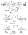
- FIG. 2 shows a scheme of a channel signal processor with a selective amplifier and a AGC circuit, of a TV reception headend belonging to the prior art, where P1 is an individual channel processor among n processors, comprising at least one tuneable channel filter, in this example two filters 9,11 interconnected to a variable gain amplifier 10 (VGA), a fixed gain amplifier 12, an individual line 20-1 for specific processor P1 signal transmission, a sample socket 40, a detector 22, a reference voltage 23, a comparator 24, a dc voltage amplifier 25, and an individual line C1 of the particular control voltage Vagc-1 applied to the corresponding processor P1.
- VGA variable gain amplifier
- Each processing module P1-Pn in the same number as the "n" reception tuned channels of the TV reception headend, incorporates a AGC loop like that featured in FIG.
- the AGC loop response time is usually high -from tenths of a second to seconds -, and the gain high, and therefore the error in the output signal 30 level is low -fractions of dB-.
- the AGC loop circuit represented in FIG. 2 works by modifying the amplification chain gain 9-12 of only one signal processor P1, until it equalises the output level of the specified channel to a reference level.
- the channel signal 20-1 output level is converted from the sample 21 to a Vdc voltage for its comparison with a prefixed reference Vdc voltage value 23.
- the Vdc voltage equivalent to the controlled output level must be determined depending on the "L" level of the specified channel, without any input level contributions from the adjacent channels n-3 to n-1 and n+1 to n+3, as is represented in FIG. 3A .
- the same processor P1-Pn provides the "rejection of adjacent channels effect".
- Adjacent channel rejections greater than 20 dB are considered necessary in collective aerial and Cable TV networks.
- the signal resultant difference is also termed error signal, and controls the gain of the amplification chain 9-12 of the processor P1 thus closing the loop of the AGC 40, 25, C1.
- FIGS. 3A and 3B represent the concept of frequency selectivity.
- the processor P1 selectivity like the one represented in FIG. 2 , is a determining factor so that the output level “L” of channel “n” is not affected by the fluctuations of the adjacent channels in the CH1 input. If in the processor P1 input several adjacent channels “n-3 to n+3" ( FIG. 3A ) are present, with “not sufficient” inherent selectivity in the processor, the sample 21 of signal will be proportional to level “L” of all the “n” channels present in the input, and the variation of any of them will alter the output level of the tuned channel, in this example CH1; whose level we are trying to maintain. In the individual AGC circuit 21-25,C1 in FIG.
- US-A-6148189 describes a RF channel signal processor for a TV receiver, with an independent AGC voltages generator block, for one only processor.
- US2003/0026364-A1 describes a RF channel digital or analogue signal processor for a TV receiver, with a generator of only one AGC, and includes the information of the RF channels map on a memory.
- patent ES-A2117953 deals with an automatic equalisation circuit of channel filters amplifiers output signals, which is carried out, unlike the automatic gain control, at a prior adjustment stage of the filters, before these come into service.
- variable gain amplifiers are applied to the variable gain amplifiers, by means of a single gain adjustment circuit to control a plurality of TV channel amplifiers, carrying it out for each amplifier individually, selecting the amplifier to be controlled by a selector.
- US-A-3978422 discloses a broadband automatic gain control amplifier comprising several transistor amplifiers and incorporating a plurality of gain-controlling components connected in parallel and exercising gain control at the interstage connections between all the amplifiers so providing control loops, each responsive to signal levels at the output of the gain control amplifier at different frequencies for developing a control signal to correct the output signal level simultaneously at that frequency and at other frequencies.
- US-A-5321849 discloses a system for controlling signal level at both ends of a transmission link, comprising a control device controlling a first signal level changing device and a second signal level changing device in response to a detected level of a transmit signal adapted to be transmitted over the transmission link.
- a combining unit assimilates all information input and forms output signals which are sent to attenuation control unit to control the respective settings of the first and second signal level changing devices.
- the object of the invention is a collective aerial or cable network headend for TV, with only one common AGC circuit for the plurality of channel signal processing modules of the headend, which generates n" Vdc control voltage values in real time, each one being particular to each channel, and applied simultaneously to the corresponding processor, thus the processors pre-established output levels are always maintained constant.
- the headend proposed by the present invention is applied to the reception of TV signals through a collective aerial or through a cable network CATV, provided with an automatic gain control of the tuned TV signals output levels, and comprises in combination:
- Said headend comprises an output or amplification line common to all the processing modules outputs, to which it is connected, directly or through a samples socket (tap), to an input of said automatic gain control circuit, in such a way that all the output signals of said processing modules, or all the samples of said signals, arrive at the same time to the automatic gain control circuit, which is governed by at least one microcontroller for:
- the selectivity of each processor needs not to be sufficient.
- the precision of the AGC common circuit becomes independent from the processors selectivity and the fluctuations of the voltage level of the adjacent channels. This is due to the incorporation in said automatic gain control circuit, of selecting means adapted to select, in a sequential manner, said processing modules output signals, or said samples of the same, one by one, through a selectivity characteristic of sufficient frequency so as to disregard the influence of the adjacent channels, at least from n-3 to n+3, being n the nominal channel corresponding to the output signal selected at any time.
- the gain control circuit of the headend proposed is provided with a microcontroller with a particular configuration data memory of the analogue and digital RF channels and a low-pass filter, and is designed for the generation of the dc AGC voltage values particular to each processor and in each moment of control, therefore a constant output level of all the signal processors of each channel n, is obtained using only one AGC circuit common to all the processors.
- the nominal frequency of each channel is sequentially selected from a memory, which is previously provided with reference numeric data corresponding to the required nominal frequencies in the "n" analogue and digital channels of the TV headend.
- Input level variations in stationary TV reception systems are slow; therefore the long period of time that passes during an input level variation enables the AGC common circuit of the invention to obtain a control response for the plurality of the TV headend processors.
- this common AGC circuit is not always applicable, due to the speed of the variations of the input levels.
- One unique circuit provided with a voltages generator block governed by a microcontroller and a reference numeric data memory, controls the "n” processing modules in real time, substituting the "n” individual AGC circuits like that in FIG. 2 . For this purpose it is necessary that the generation time of the "n" reference frequencies is less than the response time of each particular AGC.
- a common detector is connected to a low-pass filter, in whose input all the "n" channels are present, and in its output only the signal frequency corresponding to a processed nominal channel n, sequentially separated one from the others.
- the output signal sample of the common detector only contains the "L” level of the specified "n” channel, hence the selectivity of the frequency inherent in each processor is not a determining factor in the precision of the output level "L” achieved, the selectivity being always high.
- Said stored reference numeric data correspond to each signal frequency of all the channels present, the programmed ones and the possible ones in a determined headend, and are selected in a determined sequence for the generation of each specific gain control voltage Vdc value applied at the time to each processor.
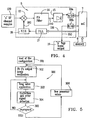
- a SMATV/MATV or CATV headend 1 comprises a plurality of processors P1-Pn, each one having as an example a chain of filters 9,11, and other devices suitable for at least filtering, and at least a variable gain amplifier 10, and they process the signals of "n" tuned channels CH1-CHn.
- the processors P1-Pn transmit all their amplified signals to a common amplification line 2 and a common output 3 of the TV headend, with each output signal maintaining a level L.
- a sample of each one of "n" channel signals present is taken by the socket (block 4), and are transmitted to a unique automatic gain control circuit AGC common to all the processors Pn, from a common line 120 of the samples socket 4, to a sequential dc voltage Vdc generator 5, a selecting, sampling and holding block 6, provided with "n” Vagc output terminals, and an automatic control system of the individual signals of each processor Pn.
- the selecting, holding and addressing block 6 receives the n voltage values Vagc generated from the automatic control system and transmitted, through the generator block 5 to the output 16, it samples them and holds them temporally for their addressing from an individual output connection Vagc-1 to Vagc-n to their corresponding amplification lines C1-Cn of the processing modules P1-Pn, sequentially or for a preferred embodiment, simultaneously.
- Output 16 is a continuous succession of as many Vdc voltage "n" levels as channel signals are processed in the TV headend, in the form of a pulse train with each pulse corresponding to one of said Vacg-1 to Vagc-n values.
- the holding circuit M-R of block 6 presents at each one of its outputs a Vdc voltage pulse proportional to the output level of each processor Pn, and maintains constant the level of each pulse to address them as AGC voltages Vagc-1 to Vagc-n, to the corresponding variable gain amplifier 10, maintaining said voltage levels constant until a possible later refreshment cycle
- the automatic gain control circuit AGC comprises in the interior of said Vdc voltage generator block 5, and interconnected, a mixer 13, a VCO (Voltage Controlled Oscillator) 18, a P.L.L. (Phase Lock Loop) circuit 17, a low pass filter 14, a detector 15 and associated to block 5 the mentioned automatic control system, formed by a microcontroller 7, a memory 8, and a keyboard display 7a.
- the group of devices 17, 18 governed by the microcontroller 7 constitutes a frequency synthesizer.
- the generator block 5 comprises in addition an A/D converter 19a and a D/A converter 19b communicated by a respective microcontroller 7 bus.
- the numeric data corresponding to division factors for the P.L.L. circuit is stored on the memory 8 of the ACG common circuit, each one of them corresponding to each reference signal frequency generated, each one representative of all the possible reception channels on the headend, as an example up to 99 different channels for a plurality of geographical areas.
- the memory stores the numeric data corresponding to the division factors representative of only the n frequency reference values required by a specific TV headend, for example 16 values (in a certain geographical area) of the n channels tuned on the headend 1 of the installed TV.
- This last part of the memory with only the required numeric data is selected by the microcontroller 7 from the total store 8, through the keyboard when the installer of the headend carries out the channel programming.
- the microcontroller 7 extracts this n numeric data for its uninterrupted use in the synthesiser block 7,17,18 and the generation of successive sequences of n frequency reference values, transmitted in the AGC common circuit for the sequential generation of n Vdc values in the output.
- the frequency synthesiser 17, 18 generates n signals of the same frequency f as the n channels that are applied to a line 180 taken to the mixer 13, in a non-interrupted sequential manner.
- the channel frequency generation sequence f is programmed through the keyboard 7a and is loaded in the memory 8.
- the microcontroller 7, following the flow diagram sequence in FIG. 5 continually pilots the P.L.L. 17 that controls the voltage controlled oscillator VCO 18 and whose output 180 is permanently applied to the mixer 13.
- a large amount of signals are present, product of the mix of the n input channels with the sequence of the n signals separated one from the other generated by the VCO 18.
- the low pass filter 14 has a cut-off frequency lower than half of the channel n bandwidth; filtered at each moment, blocking DC offsets at its input, and selects a level input L that within a sequence corresponds to the programmed channels. From output 140 of the low pass filter 14 only the frequency of the signal corresponding to a channel n is delivered each time, as a result of its coincidence with the channel n frequency generated by the VCO 18, hence obtaining the «sufficient» selectivity characteristic.
- the detector 15 delivers Vdc voltage pulses proportional to the levels L of the input channels to an A/D converter 19a.
- the converter A/D 19a converts the voltage Vdc pulses transmitted by the detector 15 from all the processors P1-Pn to numeric data, and the microcontroller 7 processes this numeric data associated to each input channel CH1-CHn, and modifies them if necessary depending on the analogue or digital nature of the signal, and the level of entry.
- the modification consists in a comparison with the value table of the data registered, analogue and digital, for each channel tuned in the memory map 8, and the addition or subtraction of an additional Vdc voltage until obtaining the appropriate Vagc voltage for the controlled processor P1-Pn, necessary to obtain the pre-established output level or the direct supply of said voltage Vagc selected from said table.
- the D/A converter 19b converts the modified numeric data in Vdc voltage pulses, as Vagc output voltages 16 suitable for obtaining the output level of each pre-established channel n, and transmits them to the demultiplexing block 6 for their application to each processor amplification line C1-Cn.
- the selectivity of the low-pass filter 14 guarantees that the level of the passing signal is proportional only to the specific channel n of each processor P1-Pn, and also when the processor P1-Pn does not have the inherent selectivity necessary to avoid that the pulse levels be altered by the level variation of the adjacent channels n-3 to n+3.
- a flow diagram 300 has been represented of the process that the microcontroller 7 follows, to emit n AGC voltage values in the common output 16 of the automatic gain control circuit AGC of the n output signals shown in FIG.1 and FIG. 4 .
- the microcontroller 7 has previously loaded the configuration data from the tables contained in the map of RF channels stored in the memory 8 -stage 301-. This information from the map includes a table of reference voltage values, pre-established by the manufacturer of the TV headend 1, for each one of the tuneable channels CH1-CHn, for a plurality of geographical areas of both possible types of signal, analogue or digital.
- the microcontroller 7 through the bus 130 that communicates with the PLL block 17, controls the latter to carry out a sequential exploration and verification through all the signal frequencies generated by the voltage controlled oscillator VCO 18, of all the channels CH1-CHn programmed in the processors P1-Pn -stage 302-, making an output level comparison of each signal delivered sequentially by the low pass filter 14, with said numeric data registered from the information map of the memory 8, and finding the coincidence to determine the Vagc initial value appropriate for each one of the processors P1-Pn.
- the microcontroller 7 detects the error signal of the input signal samples 120 of all the channels CH1-CHn previously converted to numeric data by the A/D 19a converter, and carries out a correction modifying them by comparison as described above, and converting them to Vagc voltages in the output 16 through a D/A converter 19b.
- These voltages Vagc-1 and Vagc-n are already the appropriate values in real time to maintain the n levels of the pre-established signals in the output 3 of the TV headend 1, for the programmed channel CH1-CHn in each processor P1-Pn.
- a new channel frequency value -stage 306- is assigned to the reprogrammed processor with the new channel value to carry out the routine 302-304 now.
- the method comprises the following stages to be carried out for a determined geographical area:
Abstract
Description
- The present invention relates to the reception and transmission of RF signals from collective TV aerials and cable television networks CATV, comprising a reception headend with a plurality of processing modules of the input channels signals and with an automatic gain control (AGC) applied to the signal processors.
- The reception headend of collective TV installations and of CATV cable networks, wherein it is necessary to maintain constant the output level of the signal in each channel processor of the headend, to guarantee the availability of the service offered by the operator in the user's TV sockets are known. The output level variation depends on the input power level variations and on the variation of the processor transfer function, which is generally caused by variations in the physical propagation path, ambient temperature, supply voltage, etc.
- The output level of each processor is obtained in the known TV headends, by the inclusion of an automatic gain control circuit -AGC- in each channel signal processor. The AGC loop in a channel signal processor in a TV headend must look for the balance between the error in the output level, the stability with respect to transients and the distortion in the intelligent signal.
- This function depends on the type of modulation of the carrier signal received in the headend, on the bandwidth of the intelligent signal and on the type of processor, whether the latter be stationary or mobile. The case of the situations with the presence of adjacent channels "n-3 to n+3" at the input is critical in order to obtain a constant output level "L" in channel "n". In the TV headend of the prior art, band selecting of each processor is conditioned by its own circuit, provided by the tuneable filters, any of which can be affected by the presence of the adjacent channels, making their selectivity "insufficient". The precision obtained in the gain control (AGC) of each headend processor depends on the processor "sufficient selectivity".
-
Figure 2 shows a scheme of a channel signal processor with a selective amplifier and a AGC circuit, of a TV reception headend belonging to the prior art, where P1 is an individual channel processor among n processors, comprising at least one tuneable channel filter, in this example twofilters fixed gain amplifier 12, an individual line 20-1 for specific processor P1 signal transmission, asample socket 40, adetector 22, areference voltage 23, acomparator 24, adc voltage amplifier 25, and an individual line C1 of the particular control voltage Vagc-1 applied to the corresponding processor P1. Each processing module P1-Pn, in the same number as the "n" reception tuned channels of the TV reception headend, incorporates a AGC loop like that featured inFIG. 2 from an individual line 20-1 to 20-n. For the stationary processors the AGC loop response time is usually high -from tenths of a second to seconds -, and the gain high, and therefore the error in theoutput signal 30 level is low -fractions of dB-. - The AGC loop circuit represented in
FIG. 2 , works by modifying the amplification chain gain 9-12 of only one signal processor P1, until it equalises the output level of the specified channel to a reference level. The channel signal 20-1 output level is converted from thesample 21 to a Vdc voltage for its comparison with a prefixed referenceVdc voltage value 23. The Vdc voltage equivalent to the controlled output level must be determined depending on the "L" level of the specified channel, without any input level contributions from the adjacent channels n-3 to n-1 and n+1 to n+3, as is represented inFIG. 3A . I.e. the same processor P1-Pn provides the "rejection of adjacent channels effect". Adjacent channel rejections greater than 20 dB are considered necessary in collective aerial and Cable TV networks. The signal resultant difference is also termed error signal, and controls the gain of the amplification chain 9-12 of the processor P1 thus closing the loop of theAGC -
FIGS. 3A and 3B represent the concept of frequency selectivity. The processor P1 selectivity like the one represented inFIG. 2 , is a determining factor so that the output level "L" of channel "n" is not affected by the fluctuations of the adjacent channels in the CH1 input. If in the processor P1 input several adjacent channels "n-3 to n+3" (FIG. 3A ) are present, with "not sufficient" inherent selectivity in the processor, thesample 21 of signal will be proportional to level "L" of all the "n" channels present in the input, and the variation of any of them will alter the output level of the tuned channel, in this example CH1; whose level we are trying to maintain. In the individual AGC circuit 21-25,C1 inFIG. 2 , with the adjacent channel input levels being measured together with the channel CH1 nominal level, the precision of the value of the dc voltage generated for the AGC of the processor P1 will be wrong when the adjacent channels level is the same or greater than the nominal level of the CH1 processed channel. -
US-A-6148189 describes a RF channel signal processor for a TV receiver, with an independent AGC voltages generator block, for one only processor. -
US2003/0026364-A1 describes a RF channel digital or analogue signal processor for a TV receiver, with a generator of only one AGC, and includes the information of the RF channels map on a memory. - On the other hand patent
ES-A2117953 - To obtain this equalisation corresponding gain voltages are applied to the variable gain amplifiers, by means of a single gain adjustment circuit to control a plurality of TV channel amplifiers, carrying it out for each amplifier individually, selecting the amplifier to be controlled by a selector.
-
US-A-3978422 discloses a broadband automatic gain control amplifier comprising several transistor amplifiers and incorporating a plurality of gain-controlling components connected in parallel and exercising gain control at the interstage connections between all the amplifiers so providing control loops, each responsive to signal levels at the output of the gain control amplifier at different frequencies for developing a control signal to correct the output signal level simultaneously at that frequency and at other frequencies. -
US-A-5321849 discloses a system for controlling signal level at both ends of a transmission link, comprising a control device controlling a first signal level changing device and a second signal level changing device in response to a detected level of a transmit signal adapted to be transmitted over the transmission link. A combining unit assimilates all information input and forms output signals which are sent to attenuation control unit to control the respective settings of the first and second signal level changing devices. - The object of the invention is a collective aerial or cable network headend for TV, with only one common AGC circuit for the plurality of channel signal processing modules of the headend, which generates n" Vdc control voltage values in real time, each one being particular to each channel, and applied simultaneously to the corresponding processor, thus the processors pre-established output levels are always maintained constant.
- The headend proposed by the present invention is applied to the reception of TV signals through a collective aerial or through a cable network CATV, provided with an automatic gain control of the tuned TV signals output levels, and comprises in combination:
- a plurality of processing modules arranged in parallel, and adapted to simultaneously process analogue or digital input signals of RF channels to be tuned, one channel per processing module, providing each one of said processing modules at least one filtering and each one comprising at least one variable gain amplifier with an application line of voltage gain, and
- an automatic gain control circuit responsible for processing the output signals of said processing modules, with said output signals corresponding to the tuned channels for each one of them, or samples of the same, to check output levels of the processing modules output signals and to generate and apply gain voltages to said application lines of said variable gain amplifiers so as to automatically control said output levels of the output signals of said processing modules, until they are adjusted to certain predetermined values, hence obtaining said control.
- Said headend comprises an output or amplification line common to all the processing modules outputs, to which it is connected, directly or through a samples socket (tap), to an input of said automatic gain control circuit, in such a way that all the output signals of said processing modules, or all the samples of said signals, arrive at the same time to the automatic gain control circuit, which is governed by at least one microcontroller for:
- selecting one by one, said output signals of the processing modules or said samples, using highly selective selecting means (to be explained later);
- Carrying out sequentially at least one processing of each one of said signals or selected samples (task carried out by the microcontroller itself), and
- Carrying out sequentially said generation of said gain voltages from the result of said processing of each signal or sample, whose task is carried out by said microcontroller consulting the memory data and with the support of a corresponding D/A converter.
- With this obtaining that with only one automatic gain control circuit all the headend processing modules can be controlled without having to interrupt the working of any of them.
- In the headend of the invention the selectivity of each processor needs not to be sufficient. The precision of the AGC common circuit becomes independent from the processors selectivity and the fluctuations of the voltage level of the adjacent channels. This is due to the incorporation in said automatic gain control circuit, of selecting means adapted to select, in a sequential manner, said processing modules output signals, or said samples of the same, one by one, through a selectivity characteristic of sufficient frequency so as to disregard the influence of the adjacent channels, at least from n-3 to n+3, being n the nominal channel corresponding to the output signal selected at any time.
- The gain control circuit of the headend proposed is provided with a microcontroller with a particular configuration data memory of the analogue and digital RF channels and a low-pass filter, and is designed for the generation of the dc AGC voltage values particular to each processor and in each moment of control, therefore a constant output level of all the signal processors of each channel n, is obtained using only one AGC circuit common to all the processors. The nominal frequency of each channel is sequentially selected from a memory, which is previously provided with reference numeric data corresponding to the required nominal frequencies in the "n" analogue and digital channels of the TV headend.
- Input level variations in stationary TV reception systems are slow; therefore the long period of time that passes during an input level variation enables the AGC common circuit of the invention to obtain a control response for the plurality of the TV headend processors. In mobile TV headends this common AGC circuit is not always applicable, due to the speed of the variations of the input levels. One unique circuit provided with a voltages generator block governed by a microcontroller and a reference numeric data memory, controls the "n" processing modules in real time, substituting the "n" individual AGC circuits like that in
FIG. 2 . For this purpose it is necessary that the generation time of the "n" reference frequencies is less than the response time of each particular AGC. - A common detector is connected to a low-pass filter, in whose input all the "n" channels are present, and in its output only the signal frequency corresponding to a processed nominal channel n, sequentially separated one from the others. The output signal sample of the common detector only contains the "L" level of the specified "n" channel, hence the selectivity of the frequency inherent in each processor is not a determining factor in the precision of the output level "L" achieved, the selectivity being always high. Said stored reference numeric data correspond to each signal frequency of all the channels present, the programmed ones and the possible ones in a determined headend, and are selected in a determined sequence for the generation of each specific gain control voltage Vdc value applied at the time to each processor.
- On doing away with an individual AGC circuit, in addition to economic benefits, it provides the headend with a reduction of the overall volume and an improvement in design of an exterior housing of an individual processor module.
-
-
Figure 1 shows the scheme of a TV reception headend of the invention. -
Figure 2 shows a diagram of a selective amplifier with AGC of a TV reception headend pertaining to the prior art. -
Figures 3A and 3B show a representative diagram of the frequency selectivity in the TV reception headend offigure 2 . -
Figure 4 shows a Vdc sequential voltage generator scheme for the AGC infigure 1 . -
Figure 5 shows a flow chart of the process followed by the sequential generator offigures 1 and3 . - Referring to
FIG. 1 andFIGS. 4-5 , an embodiment of theheadend 1 of TV collective aerial or cable network CATV is described as follows. A SMATV/MATV orCATV headend 1 comprises a plurality of processors P1-Pn, each one having as an example a chain offilters variable gain amplifier 10, and they process the signals of "n" tuned channels CH1-CHn. The processors P1-Pn transmit all their amplified signals to acommon amplification line 2 and acommon output 3 of the TV headend, with each output signal maintaining a level L. A sample of each one of "n" channel signals present is taken by the socket (block 4), and are transmitted to a unique automatic gain control circuit AGC common to all the processors Pn, from acommon line 120 of thesamples socket 4, to a sequential dcvoltage Vdc generator 5, a selecting, sampling and holding block 6, provided with "n" Vagc output terminals, and an automatic control system of the individual signals of each processor Pn. The selecting, holding and addressing block 6, receives the n voltage values Vagc generated from the automatic control system and transmitted, through thegenerator block 5 to theoutput 16, it samples them and holds them temporally for their addressing from an individual output connection Vagc-1 to Vagc-n to their corresponding amplification lines C1-Cn of the processing modules P1-Pn, sequentially or for a preferred embodiment, simultaneously. -
Output 16 is a continuous succession of as many Vdc voltage "n" levels as channel signals are processed in the TV headend, in the form of a pulse train with each pulse corresponding to one of said Vacg-1 to Vagc-n values. The holding circuit M-R of block 6 presents at each one of its outputs a Vdc voltage pulse proportional to the output level of each processor Pn, and maintains constant the level of each pulse to address them as AGC voltages Vagc-1 to Vagc-n, to the correspondingvariable gain amplifier 10, maintaining said voltage levels constant until a possible later refreshment cycle - Referring to
FIG. 4 , the automatic gain control circuit AGC, comprises in the interior of said Vdcvoltage generator block 5, and interconnected, amixer 13, a VCO (Voltage Controlled Oscillator) 18, a P.L.L. (Phase Lock Loop)circuit 17, alow pass filter 14, a detector 15 and associated to block 5 the mentioned automatic control system, formed by amicrocontroller 7, a memory 8, and akeyboard display 7a. The group ofdevices microcontroller 7 constitutes a frequency synthesizer. Thegenerator block 5 comprises in addition an A/D converter 19a and a D/A converter 19b communicated by arespective microcontroller 7 bus. Bothconverters microcontroller 7, enable themicrocontroller 7 operation controlling the different Vagc depending on the nature of the analogue or digital signals, without the need to use a device for the generation of reference Vdc voltages and their comparison, as each headend processor of the prior art does it (FIG. 2 ). - The numeric data corresponding to division factors for the P.L.L. circuit is stored on the memory 8 of the ACG common circuit, each one of them corresponding to each reference signal frequency generated, each one representative of all the possible reception channels on the headend, as an example up to 99 different channels for a plurality of geographical areas. On the other side the memory stores the numeric data corresponding to the division factors representative of only the n frequency reference values required by a specific TV headend, for example 16 values (in a certain geographical area) of the n channels tuned on the
headend 1 of the installed TV. This last part of the memory with only the required numeric data is selected by themicrocontroller 7 from the total store 8, through the keyboard when the installer of the headend carries out the channel programming. Themicrocontroller 7 extracts this n numeric data for its uninterrupted use in thesynthesiser block - At the
mixer input 13 the existing n channels are permanently applied. Thefrequency synthesiser line 180 taken to themixer 13, in a non-interrupted sequential manner. The channel frequency generation sequence f is programmed through thekeyboard 7a and is loaded in the memory 8. Themicrocontroller 7, following the flow diagram sequence inFIG. 5 , continually pilots the P.L.L. 17 that controls the voltage controlledoscillator VCO 18 and whoseoutput 180 is permanently applied to themixer 13. At the mixer output 13 a large amount of signals are present, product of the mix of the n input channels with the sequence of the n signals separated one from the other generated by theVCO 18. Thelow pass filter 14 has a cut-off frequency lower than half of the channel n bandwidth; filtered at each moment, blocking DC offsets at its input, and selects a level input L that within a sequence corresponds to the programmed channels. Fromoutput 140 of thelow pass filter 14 only the frequency of the signal corresponding to a channel n is delivered each time, as a result of its coincidence with the channel n frequency generated by theVCO 18, hence obtaining the «sufficient» selectivity characteristic. - The detector 15 delivers Vdc voltage pulses proportional to the levels L of the input channels to an A/
D converter 19a. The converter A/D 19a converts the voltage Vdc pulses transmitted by the detector 15 from all the processors P1-Pn to numeric data, and themicrocontroller 7 processes this numeric data associated to each input channel CH1-CHn, and modifies them if necessary depending on the analogue or digital nature of the signal, and the level of entry. The modification consists in a comparison with the value table of the data registered, analogue and digital, for each channel tuned in the memory map 8, and the addition or subtraction of an additional Vdc voltage until obtaining the appropriate Vagc voltage for the controlled processor P1-Pn, necessary to obtain the pre-established output level or the direct supply of said voltage Vagc selected from said table. The D/A converter 19b converts the modified numeric data in Vdc voltage pulses, asVagc output voltages 16 suitable for obtaining the output level of each pre-established channel n, and transmits them to the demultiplexing block 6 for their application to each processor amplification line C1-Cn. In this way the selectivity of the low-pass filter 14 guarantees that the level of the passing signal is proportional only to the specific channel n of each processor P1-Pn, and also when the processor P1-Pn does not have the inherent selectivity necessary to avoid that the pulse levels be altered by the level variation of the adjacent channels n-3 to n+3. - With reference to
FIG. 5 , a flow diagram 300 has been represented of the process that themicrocontroller 7 follows, to emit n AGC voltage values in thecommon output 16 of the automatic gain control circuit AGC of the n output signals shown inFIG.1 andFIG. 4 . Themicrocontroller 7 has previously loaded the configuration data from the tables contained in the map of RF channels stored in the memory 8 -stage 301-. This information from the map includes a table of reference voltage values, pre-established by the manufacturer of theTV headend 1, for each one of the tuneable channels CH1-CHn, for a plurality of geographical areas of both possible types of signal, analogue or digital. Themicrocontroller 7 through thebus 130 that communicates with thePLL block 17, controls the latter to carry out a sequential exploration and verification through all the signal frequencies generated by the voltage controlledoscillator VCO 18, of all the channels CH1-CHn programmed in the processors P1-Pn -stage 302-, making an output level comparison of each signal delivered sequentially by thelow pass filter 14, with said numeric data registered from the information map of the memory 8, and finding the coincidence to determine the Vagc initial value appropriate for each one of the processors P1-Pn. Then - stage 303- the AGC determined voltages, Vagc-1 to Vagc-n are applied without interruption through theoutput 16 of thegenerator block 5, to the block 6 and from here to the supply line C1-Cn of the corresponding AGC of each processor P1-Pn. - In the
stage 304 that follows the sampling of the channels CH1-CHn and the sequential application of each one of the Vagc voltages obtained, themicrocontroller 7 detects the error signal of theinput signal samples 120 of all the channels CH1-CHn previously converted to numeric data by the A/D 19a converter, and carries out a correction modifying them by comparison as described above, and converting them to Vagc voltages in theoutput 16 through a D/A converter 19b. These voltages Vagc-1 and Vagc-n are already the appropriate values in real time to maintain the n levels of the pre-established signals in theoutput 3 of theTV headend 1, for the programmed channel CH1-CHn in each processor P1-Pn. In the case of reprogramming -stage 305- some of the processors P1-Pn to a certain channel different from the previous one, a new channel frequency value -stage 306- is assigned to the reprogrammed processor with the new channel value to carry out the routine 302-304 now. - From the aforementioned an operation method is deduced for an automatic gain control circuit applied to control a TV reception headend like that proposed by the invention in order to obtain the desired output signals.
- The method comprises the following stages to be carried out for a determined geographical area:
- a) Select a table stored in said memory with information referring to said area, said table containing data groups that include the channel to be tuned, the pre-determined level L for the output signal of said tuned channel, and the initial automatic gain control voltage Vagcin;
- b) Sequentially select each one of said output signals to acquire information, for each channel, relative at least to:
- i. Output signal frequency of said channel;
- ii. Level L of said output level for the channel.
- c) Compare said information acquired for each channel with that contained in each table, and:
- i. Select a Vagcin value corresponding to said channel; or
- ii. Modify a previously channel generated value Vagc if the signal level L whose value has been acquired does not coincide with the predetermined one for said channel.
- d) Convert each one of said voltage values Vagc or modified Vagc into an analogue value and apply said analogue values, sequentially to said block 6 through said
output 16 for their eventual application to thevariable amplifiers 10 of each processing module P1.....Pn. - e) Repeat the stages b) c) y d) cyclically in a loop to maintain the control conditions at all times.
- Should reprogramming of the channels assigned to the processing module be desired, for example P1.....Pn to change geographical areas, in the stage a), a new table of values corresponding to the new assigned channels will be selected and the remaining stages will be carried out in an analogue manner.
- It will be apparent to those skilled in the art that modifications and changes may be made to the examples of the embodiments described without departing from the scope of the present invention which is defined in the following claims.
Claims (10)
- TV signals reception headend receiving signals through a collective aerial or by cable network CATV, with automatic gain control of the output levels of the tuned TV signals, that comprises in combination:- a plurality of processing modules (P1-Pn) in a parallel arrangement, and adapted to simultaneously process analogue or digital input signals of RF channels (CH1-CHn) to be tuned, a channel (CH1-CHn) per processing module (P1-Pn), each one of said processing modules (P1-Pn) providing at least filtering and each one of them comprising at least one variable gain amplifier (10) with an application line (C1-Cn) of gain voltage (Vacg-1 to Vacg-n),- an automatic gain control circuit (AGC) responsible for processing the output signals of said processing modules (P1-Pn), said output signals corresponding to the channels (CH1-CHn) tuned by each one of them, or samples of the same, to check output levels (L) of the output signals of the processing modules (P1-Pn) and to generate and apply gain voltages (Vacg-1 to Vacg-n) to said application lines (C1-Cn) of said variable gain amplifiers (10) in order to automatically control said output levels (L) of said processing modules (P1-Pn) output signals, until adjusting them to certain predetermined values, hence achieving said control,- an output or amplification line (2) common to all the processing modules (P1-Pn) outputs, which is connected, directly or through a sample socket (4), to an input of said automatic gain control circuit (AGC), so that all said processing modules (P1-Pn) output signals, or all the samples of said signals, arrive at the same time to the automatic gain control circuit (AGC), which is governed by at least one microcontroller (7) to:- select one by one, said processing modules (P1-Pn) output signals or said samples, through selection means.- carry out sequentially at least one processing of each one of said selected signals or samples; and- carry out sequentially said generation of said gain voltages (Vacg-1 to Vacg-n) from the result of said processing of each signal or sample.
- Headend according to claim 1, wherein said automatic gain control circuit (AGC) is adapted to carry out said application of gain voltages (Vacg-1 to Vacg-n) to the application lines (C1-Cn) of the variable gain amplifiers (10) in a sequential fashion.
- Headend, according to claim 1, wherein said automatic gain control circuit (AGC) is adapted to carry out said application of the gain voltages (Vacg-1 to Vacg-n) to the application lines (C1-Cn) of the variable gain amplifiers (10) in a simultaneous fashion.
- Headend, according to claim 1 or 3, wherein said automatic gain control circuit (AGC) comprises selecting means adapted for selecting, in a sequential manner, said processing modules (P1-Pn) output signals, or said samples of the same, one by one, through a frequency selectivity characteristic sufficient enough to make them independent from the influence of the adjacent channels, at least from n-3 to n+3, being n the nominal channel corresponding to the output signal selected at each moment.
- Headend, according to claim 4, wherein said automatic gain control circuit (AGC) comprises:- a Vdc voltages generator block (5) with an input connected to an output common line (120) of the sample socket (4), which is associated to an automatic control system, with at least one microcontroller (7) and one memory (8), to sequentially process said signal samples and to generate and send sequentially, said gain voltages (Vacg-1 to Vacg-n) through an output (16),- a sampling, holding and addressing block (6) with an input connected to said generator block (5) output (16), and a series of outputs each one of which individually connected to one of said amplification lines (C1-Cn) of the processing modules (P1-Pn), with said block (6) also associated to said automatic control system, and controlled by the same, to sample and temporally hold said gain voltages (Vacg-1 to Vacg-n) and to address them to their corresponding amplification lines (C1-Cn) of the processing modules (P1-Pn).
- Headend, according to claim 5, wherein said memory (8) stores at least numeric data representative of the headend configuration for at least all the analogue and digital channels (CH1-CHn) to be received by said TV headend, in at least one geographical area, with their corresponding frequencies, with respective division factors, as well as of output signals levels (L) which are pre-established for each analogue or digital channel (CH1-CHn), and respective gain voltages, at least initial gain voltages.
- Headend, according to claim 6, wherein said automatic control system is adapted for, by means of at least said microcontroller (7), receiving values of Vdc voltage pulses proportional to the values sampled at said samples socket (4) and generated by said generator block (5), for each channel (CH1-CHn), and, after its digitalisation by a corresponding A/D converter (19a), comparing them with said data relative to said levels (L) stored in the memory (8), and depending on the result of said comparisons sending to said generator block (5) digital values referring to said initial or modified gain voltages, that said generator block (5) converts to analogue, through a corresponding D/A converter (19b), and sending them through said output (16).
- Headend, according to claim 7, wherein said generator block (5) comprises:- at least part of said selection means comprising at least a frequency synthesiser (17-18), a mixer (13) with an input connected to the output of said synthesiser (17-18) and another input connected to said common line (120) through which the input signals samples are received, a low-pass filter (14) of a cut-off frequency lower than half of the bandwidth of the channel n to be filtered in each moment and blocking a possible DC offset at its input, connected to the output of said mixer (13), simultaneously receiving all the signals corresponding to all the tuned channels (CH1-CHn), said microcontroller (7) also forming part of said selection means to control, through a corresponding output (130), said synthesiser (17-18) in order to supply a series of signals with frequencies equal to the ones of all the channels (CH1-CHn), one by one following an uninterrupted sequence,- a detector (15) with an input connected to the output of said low-pass filter (14), and an output to said A/D converter (19a).
- Headend, according to claim 6, wherein said storage memory (8) stores numeric data representative of a plurality of configurations of the headend for analogue and digital channels to be received by said TV headend, in a plurality of geographical areas, with their corresponding frequencies as well as of output signals levels (L) which are pre-established for each channel and some respective initial gain voltages.
- Headend according to claim 9, wherein said automatic gain control circuit (AGC) further comprises, in association with said microcontroller (7), a display and a keyboard (7a), to respectively visualise at least part of said data corresponding to said plurality of configurations, and select those which correspond to one of said configurations, in order to re-programme the processing modules (P1-Pn) through a corresponding channels reassignment, and their associated data referring to desired levels (L) and corresponding gain voltages, at least initial gain voltages.
Priority Applications (1)
| Application Number | Priority Date | Filing Date | Title |
|---|---|---|---|
| PL05023505T PL1653609T3 (en) | 2004-10-27 | 2005-10-27 | TV reception headend, with circuit for automatic control of output levels |
Applications Claiming Priority (1)
| Application Number | Priority Date | Filing Date | Title |
|---|---|---|---|
| ES200402578A ES2259888B1 (en) | 2004-10-27 | 2004-10-27 | TV RECEPTION HEADER, WITH AN AUTOMATIC CONTROL CIRCUIT OF OUTPUT LEVELS. |
Publications (2)
| Publication Number | Publication Date |
|---|---|
| EP1653609A1 EP1653609A1 (en) | 2006-05-03 |
| EP1653609B1 true EP1653609B1 (en) | 2008-03-05 |
Family
ID=35613631
Family Applications (1)
| Application Number | Title | Priority Date | Filing Date |
|---|---|---|---|
| EP05023505A Not-in-force EP1653609B1 (en) | 2004-10-27 | 2005-10-27 | TV reception headend, with circuit for automatic control of output levels |
Country Status (6)
| Country | Link |
|---|---|
| EP (1) | EP1653609B1 (en) |
| AT (1) | ATE388519T1 (en) |
| DE (1) | DE602005005133D1 (en) |
| ES (2) | ES2259888B1 (en) |
| PL (1) | PL1653609T3 (en) |
| PT (1) | PT1653609E (en) |
Families Citing this family (4)
| Publication number | Priority date | Publication date | Assignee | Title |
|---|---|---|---|---|
| EP2040470A1 (en) * | 2007-09-20 | 2009-03-25 | FAGOR, S.Coop | Programmable active distributor for a TV headend |
| ES2356759A1 (en) * | 2008-09-23 | 2011-04-13 | Televes, S.A. | Device with a circuit for processing telecommunication signals |
| CN101577530B (en) * | 2009-06-05 | 2012-09-05 | 中兴通讯股份有限公司 | Multi-passage power control circuit and method thereof |
| EP2393291B1 (en) | 2010-06-07 | 2012-12-19 | Angel Iglesias S.A. | Programmable amplifier for television channels |
Family Cites Families (7)
| Publication number | Priority date | Publication date | Assignee | Title |
|---|---|---|---|---|
| US3978422A (en) * | 1975-02-28 | 1976-08-31 | Alpha Engineering Corporation | Broadband automatic gain control amplifier |
| US4987606A (en) * | 1988-12-21 | 1991-01-22 | Matsushita Electric Industrial Co., Ltd. | Wide band transmission system with biasing of gain control circuit |
| JPH02266708A (en) * | 1989-04-07 | 1990-10-31 | Pioneer Electron Corp | Setting circuit for frequency characteristic of amplifier |
| JP2643543B2 (en) * | 1990-06-20 | 1997-08-20 | 日本電気株式会社 | CATV transmission equalization method |
| US5321849A (en) * | 1991-05-22 | 1994-06-14 | Southwestern Bell Technology Resources, Inc. | System for controlling signal level at both ends of a transmission link based on a detected valve |
| JP3554218B2 (en) * | 1999-03-17 | 2004-08-18 | 富士通株式会社 | Power control circuit and transmitter |
| SG93224A1 (en) * | 2000-02-02 | 2002-12-17 | Koninkl Philips Electronics Nv | Measuring antenna signal strength with automatic gain control receiver |
-
2004
- 2004-10-27 ES ES200402578A patent/ES2259888B1/en not_active Expired - Fee Related
-
2005
- 2005-10-27 PT PT05023505T patent/PT1653609E/en unknown
- 2005-10-27 PL PL05023505T patent/PL1653609T3/en unknown
- 2005-10-27 ES ES05023505T patent/ES2300922T3/en active Active
- 2005-10-27 AT AT05023505T patent/ATE388519T1/en not_active IP Right Cessation
- 2005-10-27 EP EP05023505A patent/EP1653609B1/en not_active Not-in-force
- 2005-10-27 DE DE602005005133T patent/DE602005005133D1/en active Active
Also Published As
| Publication number | Publication date |
|---|---|
| PL1653609T3 (en) | 2008-08-29 |
| DE602005005133D1 (en) | 2008-04-17 |
| ES2259888A1 (en) | 2006-10-16 |
| PT1653609E (en) | 2008-04-22 |
| ATE388519T1 (en) | 2008-03-15 |
| ES2259888B1 (en) | 2007-10-01 |
| EP1653609A1 (en) | 2006-05-03 |
| ES2300922T3 (en) | 2008-06-16 |
Similar Documents
| Publication | Publication Date | Title |
|---|---|---|
| US4777653A (en) | Apparatus for controlling transmission power over a digital radio communication channel | |
| US4328581A (en) | Adaptive HF communication system | |
| EP0507926B1 (en) | Linear transmitter training method and apparatus | |
| EP1653609B1 (en) | TV reception headend, with circuit for automatic control of output levels | |
| EP1327313B1 (en) | Selectively activated agc signal measurement unit | |
| US5230012A (en) | Process and circuit arrangement for digital control of the frequency and/or phase of scanning clock pulses | |
| US5963868A (en) | Transmission controller for transmitters in base station for mobile telecommunication system | |
| JP2000270032A (en) | Power control circuit and transmitter | |
| CN100425012C (en) | Array antenna receiver device | |
| CN100581065C (en) | Regulating method for signal receiver and relevant receiver | |
| AU707026B2 (en) | Automatic tuning of a radio transceiver | |
| US5657318A (en) | Phase-comparison bit synchronizing circuit | |
| EP1368917B1 (en) | Method for power detection of multicarrier signals and radio transmission unit | |
| KR101150667B1 (en) | Receive circuit and method for receiving an ofdm signal | |
| US5697072A (en) | Transmission signal level control device for radio transmitter | |
| EP0273031B1 (en) | Characterized fast tuning control for a television system | |
| WO2002039733A2 (en) | Frequency agile adaptive automatic gain control circuit | |
| US7050466B1 (en) | Apparatus and method for acquiring multi-user signal synchronization in code division multiple access system | |
| US4271478A (en) | Method and apparatus for measuring the transmission characteristics in electrical communication systems | |
| JPH10507893A (en) | Digital data communication system and method | |
| US6522892B1 (en) | Method of controlling transmission output of radio via closed loop and open loop operation | |
| KR101043614B1 (en) | Multiplexing module and multiplexing method for reference clock | |
| JPH04299608A (en) | Automatic gain control circuit | |
| US20040198266A1 (en) | Control circuitry | |
| EP4360370A1 (en) | Time alignment of sampled radio frequency in a multi-channel receiver system |
Legal Events
| Date | Code | Title | Description |
|---|---|---|---|
| PUAI | Public reference made under article 153(3) epc to a published international application that has entered the european phase |
Free format text: ORIGINAL CODE: 0009012 |
|
| AK | Designated contracting states |
Kind code of ref document: A1 Designated state(s): AT BE BG CH CY CZ DE DK EE ES FI FR GB GR HU IE IS IT LI LT LU LV MC NL PL PT RO SE SI SK TR |
|
| AX | Request for extension of the european patent |
Extension state: AL BA HR MK YU |
|
| 17P | Request for examination filed |
Effective date: 20060517 |
|
| 17Q | First examination report despatched |
Effective date: 20060623 |
|
| AKX | Designation fees paid |
Designated state(s): AT BE BG CH CY CZ DE DK EE ES FI FR GB GR HU IE IS IT LI LT LU LV MC NL PL PT RO SE SI SK TR |
|
| GRAP | Despatch of communication of intention to grant a patent |
Free format text: ORIGINAL CODE: EPIDOSNIGR1 |
|
| GRAS | Grant fee paid |
Free format text: ORIGINAL CODE: EPIDOSNIGR3 |
|
| GRAA | (expected) grant |
Free format text: ORIGINAL CODE: 0009210 |
|
| AK | Designated contracting states |
Kind code of ref document: B1 Designated state(s): AT BE BG CH CY CZ DE DK EE ES FI FR GB GR HU IE IS IT LI LT LU LV MC NL PL PT RO SE SI SK TR |
|
| REG | Reference to a national code |
Ref country code: GB Ref legal event code: FG4D |
|
| REG | Reference to a national code |
Ref country code: CH Ref legal event code: EP |
|
| REG | Reference to a national code |
Ref country code: IE Ref legal event code: FG4D |
|
| REF | Corresponds to: |
Ref document number: 602005005133 Country of ref document: DE Date of ref document: 20080417 Kind code of ref document: P |
|
| REG | Reference to a national code |
Ref country code: PT Ref legal event code: SC4A Free format text: AVAILABILITY OF NATIONAL TRANSLATION Effective date: 20080409 |
|
| REG | Reference to a national code |
Ref country code: ES Ref legal event code: FG2A Ref document number: 2300922 Country of ref document: ES Kind code of ref document: T3 |
|
| PG25 | Lapsed in a contracting state [announced via postgrant information from national office to epo] |
Ref country code: AT Free format text: LAPSE BECAUSE OF FAILURE TO SUBMIT A TRANSLATION OF THE DESCRIPTION OR TO PAY THE FEE WITHIN THE PRESCRIBED TIME-LIMIT Effective date: 20080305 |
|
| REG | Reference to a national code |
Ref country code: PL Ref legal event code: T3 |
|
| NLV1 | Nl: lapsed or annulled due to failure to fulfill the requirements of art. 29p and 29m of the patents act | ||
| PG25 | Lapsed in a contracting state [announced via postgrant information from national office to epo] |
Ref country code: LV Free format text: LAPSE BECAUSE OF FAILURE TO SUBMIT A TRANSLATION OF THE DESCRIPTION OR TO PAY THE FEE WITHIN THE PRESCRIBED TIME-LIMIT Effective date: 20080305 Ref country code: SI Free format text: LAPSE BECAUSE OF FAILURE TO SUBMIT A TRANSLATION OF THE DESCRIPTION OR TO PAY THE FEE WITHIN THE PRESCRIBED TIME-LIMIT Effective date: 20080305 Ref country code: BE Free format text: LAPSE BECAUSE OF FAILURE TO SUBMIT A TRANSLATION OF THE DESCRIPTION OR TO PAY THE FEE WITHIN THE PRESCRIBED TIME-LIMIT Effective date: 20080305 |
|
| PG25 | Lapsed in a contracting state [announced via postgrant information from national office to epo] |
Ref country code: NL Free format text: LAPSE BECAUSE OF FAILURE TO SUBMIT A TRANSLATION OF THE DESCRIPTION OR TO PAY THE FEE WITHIN THE PRESCRIBED TIME-LIMIT Effective date: 20080305 Ref country code: SK Free format text: LAPSE BECAUSE OF FAILURE TO SUBMIT A TRANSLATION OF THE DESCRIPTION OR TO PAY THE FEE WITHIN THE PRESCRIBED TIME-LIMIT Effective date: 20080305 |
|
| PG25 | Lapsed in a contracting state [announced via postgrant information from national office to epo] |
Ref country code: RO Free format text: LAPSE BECAUSE OF FAILURE TO SUBMIT A TRANSLATION OF THE DESCRIPTION OR TO PAY THE FEE WITHIN THE PRESCRIBED TIME-LIMIT Effective date: 20080305 |
|
| ET | Fr: translation filed | ||
| PG25 | Lapsed in a contracting state [announced via postgrant information from national office to epo] |
Ref country code: IS Free format text: LAPSE BECAUSE OF FAILURE TO SUBMIT A TRANSLATION OF THE DESCRIPTION OR TO PAY THE FEE WITHIN THE PRESCRIBED TIME-LIMIT Effective date: 20080705 |
|
| PLBE | No opposition filed within time limit |
Free format text: ORIGINAL CODE: 0009261 |
|
| STAA | Information on the status of an ep patent application or granted ep patent |
Free format text: STATUS: NO OPPOSITION FILED WITHIN TIME LIMIT |
|
| PG25 | Lapsed in a contracting state [announced via postgrant information from national office to epo] |
Ref country code: DE Free format text: LAPSE BECAUSE OF FAILURE TO SUBMIT A TRANSLATION OF THE DESCRIPTION OR TO PAY THE FEE WITHIN THE PRESCRIBED TIME-LIMIT Effective date: 20080606 Ref country code: LT Free format text: LAPSE BECAUSE OF FAILURE TO SUBMIT A TRANSLATION OF THE DESCRIPTION OR TO PAY THE FEE WITHIN THE PRESCRIBED TIME-LIMIT Effective date: 20080305 Ref country code: DK Free format text: LAPSE BECAUSE OF FAILURE TO SUBMIT A TRANSLATION OF THE DESCRIPTION OR TO PAY THE FEE WITHIN THE PRESCRIBED TIME-LIMIT Effective date: 20080305 |
|
| 26N | No opposition filed |
Effective date: 20081208 |
|
| PG25 | Lapsed in a contracting state [announced via postgrant information from national office to epo] |
Ref country code: EE Free format text: LAPSE BECAUSE OF FAILURE TO SUBMIT A TRANSLATION OF THE DESCRIPTION OR TO PAY THE FEE WITHIN THE PRESCRIBED TIME-LIMIT Effective date: 20080305 Ref country code: BG Free format text: LAPSE BECAUSE OF FAILURE TO SUBMIT A TRANSLATION OF THE DESCRIPTION OR TO PAY THE FEE WITHIN THE PRESCRIBED TIME-LIMIT Effective date: 20080605 |
|
| PG25 | Lapsed in a contracting state [announced via postgrant information from national office to epo] |
Ref country code: MC Free format text: LAPSE BECAUSE OF NON-PAYMENT OF DUE FEES Effective date: 20081031 |
|
| PG25 | Lapsed in a contracting state [announced via postgrant information from national office to epo] |
Ref country code: CY Free format text: LAPSE BECAUSE OF FAILURE TO SUBMIT A TRANSLATION OF THE DESCRIPTION OR TO PAY THE FEE WITHIN THE PRESCRIBED TIME-LIMIT Effective date: 20080305 |
|
| PG25 | Lapsed in a contracting state [announced via postgrant information from national office to epo] |
Ref country code: IE Free format text: LAPSE BECAUSE OF NON-PAYMENT OF DUE FEES Effective date: 20081028 |
|
| REG | Reference to a national code |
Ref country code: CH Ref legal event code: PL |
|
| PG25 | Lapsed in a contracting state [announced via postgrant information from national office to epo] |
Ref country code: LU Free format text: LAPSE BECAUSE OF NON-PAYMENT OF DUE FEES Effective date: 20081027 Ref country code: HU Free format text: LAPSE BECAUSE OF FAILURE TO SUBMIT A TRANSLATION OF THE DESCRIPTION OR TO PAY THE FEE WITHIN THE PRESCRIBED TIME-LIMIT Effective date: 20080906 |
|
| PG25 | Lapsed in a contracting state [announced via postgrant information from national office to epo] |
Ref country code: CH Free format text: LAPSE BECAUSE OF NON-PAYMENT OF DUE FEES Effective date: 20091031 Ref country code: LI Free format text: LAPSE BECAUSE OF NON-PAYMENT OF DUE FEES Effective date: 20091031 |
|
| PG25 | Lapsed in a contracting state [announced via postgrant information from national office to epo] |
Ref country code: GB Free format text: LAPSE BECAUSE OF NON-PAYMENT OF DUE FEES Effective date: 20091027 |
|
| PG25 | Lapsed in a contracting state [announced via postgrant information from national office to epo] |
Ref country code: GR Free format text: LAPSE BECAUSE OF NON-PAYMENT OF DUE FEES Effective date: 20081031 |
|
| PGFP | Annual fee paid to national office [announced via postgrant information from national office to epo] |
Ref country code: TR Payment date: 20120928 Year of fee payment: 8 |
|
| PGFP | Annual fee paid to national office [announced via postgrant information from national office to epo] |
Ref country code: PL Payment date: 20130923 Year of fee payment: 9 |
|
| PGFP | Annual fee paid to national office [announced via postgrant information from national office to epo] |
Ref country code: PT Payment date: 20130429 Year of fee payment: 9 Ref country code: FR Payment date: 20131022 Year of fee payment: 9 Ref country code: CZ Payment date: 20131018 Year of fee payment: 9 Ref country code: SE Payment date: 20131022 Year of fee payment: 9 |
|
| PGFP | Annual fee paid to national office [announced via postgrant information from national office to epo] |
Ref country code: IT Payment date: 20131025 Year of fee payment: 9 Ref country code: FI Payment date: 20131011 Year of fee payment: 9 Ref country code: ES Payment date: 20131028 Year of fee payment: 9 |
|
| REG | Reference to a national code |
Ref country code: PT Ref legal event code: MM4A Free format text: LAPSE DUE TO NON-PAYMENT OF FEES Effective date: 20150427 |
|
| REG | Reference to a national code |
Ref country code: SE Ref legal event code: EUG |
|
| PG25 | Lapsed in a contracting state [announced via postgrant information from national office to epo] |
Ref country code: CZ Free format text: LAPSE BECAUSE OF NON-PAYMENT OF DUE FEES Effective date: 20141027 Ref country code: PT Free format text: LAPSE BECAUSE OF NON-PAYMENT OF DUE FEES Effective date: 20150427 Ref country code: FI Free format text: LAPSE BECAUSE OF NON-PAYMENT OF DUE FEES Effective date: 20141027 Ref country code: SE Free format text: LAPSE BECAUSE OF NON-PAYMENT OF DUE FEES Effective date: 20141028 |
|
| REG | Reference to a national code |
Ref country code: FR Ref legal event code: ST Effective date: 20150630 |
|
| PG25 | Lapsed in a contracting state [announced via postgrant information from national office to epo] |
Ref country code: IT Free format text: LAPSE BECAUSE OF NON-PAYMENT OF DUE FEES Effective date: 20141027 Ref country code: FR Free format text: LAPSE BECAUSE OF NON-PAYMENT OF DUE FEES Effective date: 20141031 |
|
| REG | Reference to a national code |
Ref country code: ES Ref legal event code: FD2A Effective date: 20151127 |
|
| PG25 | Lapsed in a contracting state [announced via postgrant information from national office to epo] |
Ref country code: ES Free format text: LAPSE BECAUSE OF NON-PAYMENT OF DUE FEES Effective date: 20141028 Ref country code: PL Free format text: LAPSE BECAUSE OF NON-PAYMENT OF DUE FEES Effective date: 20141027 |
|
| PG25 | Lapsed in a contracting state [announced via postgrant information from national office to epo] |
Ref country code: TR Free format text: LAPSE BECAUSE OF NON-PAYMENT OF DUE FEES Effective date: 20141027 |