EP1630713B1 - Rückstrahlungsabfrageverfahren und Abfragegerät für ein moduliertes Rückstrahlungssystem - Google Patents
Rückstrahlungsabfrageverfahren und Abfragegerät für ein moduliertes Rückstrahlungssystem Download PDFInfo
- Publication number
- EP1630713B1 EP1630713B1 EP04020074.3A EP04020074A EP1630713B1 EP 1630713 B1 EP1630713 B1 EP 1630713B1 EP 04020074 A EP04020074 A EP 04020074A EP 1630713 B1 EP1630713 B1 EP 1630713B1
- Authority
- EP
- European Patent Office
- Prior art keywords
- signal
- interrogator
- backscatter
- modulated backscatter
- cancellation
- Prior art date
- Legal status (The legal status is an assumption and is not a legal conclusion. Google has not performed a legal analysis and makes no representation as to the accuracy of the status listed.)
- Expired - Fee Related
Links
Images

Classifications
-
- G—PHYSICS
- G06—COMPUTING; CALCULATING OR COUNTING
- G06K—GRAPHICAL DATA READING; PRESENTATION OF DATA; RECORD CARRIERS; HANDLING RECORD CARRIERS
- G06K7/00—Methods or arrangements for sensing record carriers, e.g. for reading patterns
- G06K7/0008—General problems related to the reading of electronic memory record carriers, independent of its reading method, e.g. power transfer
-
- H—ELECTRICITY
- H04—ELECTRIC COMMUNICATION TECHNIQUE
- H04B—TRANSMISSION
- H04B1/00—Details of transmission systems, not covered by a single one of groups H04B3/00 - H04B13/00; Details of transmission systems not characterised by the medium used for transmission
- H04B1/38—Transceivers, i.e. devices in which transmitter and receiver form a structural unit and in which at least one part is used for functions of transmitting and receiving
- H04B1/40—Circuits
- H04B1/50—Circuits using different frequencies for the two directions of communication
- H04B1/52—Hybrid arrangements, i.e. arrangements for transition from single-path two-direction transmission to single-direction transmission on each of two paths or vice versa
- H04B1/525—Hybrid arrangements, i.e. arrangements for transition from single-path two-direction transmission to single-direction transmission on each of two paths or vice versa with means for reducing leakage of transmitter signal into the receiver
Definitions
- the present invention relates to a method for backscatter interrogator reception as well as to an interrogator for use in a modulated backscatter system (MBS).
- MBS modulated backscatter system
- RFID systems are known in the art and are the basis for the recently developed so-called radio frequency identification (RFID) systems. These RFID systems are for example used for identifying and/or tracking equipment, inventory, persons or animals.
- RFID systems are radio communication systems that allow communication between a radio transceiver, called an interrogator, and at least one so-called tag. In an RFID system the interrogator communicates with the tag by transmitting an unmodulated radio signal which is received, modulated and transmitted back by the tag to the interrogator.
- Fig. 1 The general idea underlying a modulated backscatter system is shown in Fig. 1 . Similar to the field of radar technology, backscatter communication is based on the idea that electromagnetic waves are reflected by an object. The efficiency with which an object reflects electromagnetic waves is described by its radar cross-section. Objects that are in resonance with the wave front that hits them, as it is the case for antennas at the appropriate frequency, for example, have a particularly large radar cross-section.
- a signal PI is emitted from a transmitting circuit 101 of interrogator 100, a small portion P1' of which reaches the antenna 111 of the tag 110.
- a proportion of the incoming power P1' is reflected by the antenna 111 of the tag 110 and returned as power P2.
- the reflection characteristics of the antenna 111 can be influenced by altering the load connected to the antenna 111.
- two different load impedance values Z and Z' in the embodiment of Fig. 1 are alternately connected with the antenna 111 in time with the data stream to be transmitted. In this way, the amplitude of the power P2 reflected from the tag 110 can be modulated resulting in a modulated backscatter signal.
- the power P2 reflected from the tag 110 is again radiated into free space wherein a small proportion P2' of this is picked up by the antenna 103 of the interrogator 100.
- the reflected signal therefore travels into the antenna connection of the interrogator 100 in the backwards direction and can be decoupled and transferred to a receiver 102 of the interrogator 100 where the signal is demodulated in order to retrieve the information transmitted by the tag 110.
- the antenna 103 can be split into a distinct transmit antenna and a separate reception antenna which are spatially separated and thereby eliminating the requirement for a de-coupler in the interrogator 100.
- an object of the present invention to overcome the problems mentioned above by providing an interrogator for use in a modulated backscatter system wherein the performance of the receiver sensitivity of the interrogator is improved.
- the present invention proposes a novel idea for reducing the effect of the leakage of the interrogating RF waveform - called inband interferer - allowing to achieve an improved receiver sensitivity.
- the inband interferer can be more than 60db stronger than the received backscatter signal.
- an one-stage inband interferer cancellation as commonly used in known prior art RFID systems cannot cancel the inband interferer efficiently enough. Accordingly, a good receiver sensitivity and a large dynamic range cannot be guaranteed.
- WO 00/21204 A discloses a system for suppressing RF signals transmitted by a transmitter from the RF signals received by a receiver.
- the RF signals transmitted by a transmitter are sampled by a coupler of the system.
- the RF signals are then applied to a modulator which adjusts the signals from the transmitter to have an equal frequency and amplitude as the RF signals from the transmitter as well as an opposite phase.
- the modulated signal is applied to the RF signals received by a receiver antenna.
- the modulated signals and signals from the transmitter cancel out which eliminates transmitter signals in the received signal.
- the resulting signal is monitored to determine the noise signals remaining in the received signal.
- the modulator is then adjusted to minimize the noise signals.
- the present invention therefore proposes an improved receiver structure, which concatenates a two-stage inband interferer cancellation scheme efficiently to eliminate the inband interferer.
- the present invention proposes an improved super-heterodyne receiver structure with which a good receiver sensitivity can be achieved.
- a backscatter interrogator reception method is proposed as defined in claim 1.
- an interrogator for use in a modulated backscatter system is provided as defined in claim 3.
- the load impedance of the antenna 111 of the tag 110 is changed for example between values representing the data signals "1" and "0".
- the interrogating radio frequency waveform reflected by the tag 110 is switched in its amplitude (and/or phase) between those two values.
- the antenna 111 becomes the electrical equivalent of a single half-wave length antenna that reflects a portion of the power; when the switch is open, the antenna 111 becomes the electrical equivalent of a two quarter wave length antenna that reflects very little of the power.
- ASK amplitude-shift-keying
- the modulated reflected signal P2 is called the MBS signal, which will be received by the interrogator 100 together with a strong inband interferer.
- the spectrum of the MBS signal shall be far away from the leakage of the interrogating RF carrier frequency (called the inband interferer), which can be implemented by the introduction of an intermediate frequency. Examples of various intermediate frequency MBS modulation schemes are shown in Fig. 2 .
- Fig. 3 shows the typical spectrum of the intermediate frequency MBS signal received by the antenna 101 of the interrogator 100 where f c is the carrier frequency of the interrogating carrier signal PI and f i is the MBS intermediate frequency.
- the power of the inband interferer is approximately 25db higher than that of the MBS reflected signal. If the range between the interrogator 100 and the tag 110 is extended, for example to more than 5 m, the power of the reflected MBS signal is further reduced by approximately 35 dB or even more. Thus, the power of the inband interferer can be about 60 dB higher than that of the MBS signal.
- the inband interferer will be multiplied with the local oscillator and an unwanted baseband noise is generated. Part of this noise overlaps with the spectrum of the MBS signal, which is proportional to the power level of the inband interferer, the round trip delay between the interrogator 100 and the tag 110 and etc. If the noise level approximates that of the MBS signal, the reflected MBS signal cannot be demodulated and a reliable data transmission cannot be guaranteed.
- the present invention now provides an improved interrogator receiver structure that allows to expand the operating range of classical modulated backscatter systems by reducing the effect of the inband interferer.
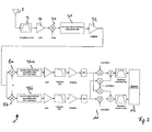
- the receiver structure proposed in accordance with the present invention is based on a known receiver structure, which is shown in Fig. 4 .
- This known structure combines the benefits of a direct down-conversion architecture with that of a low intermediate frequency (IF) architecture.
- IF intermediate frequency
- the MBS signal received by the antenna 2 passes at first a pre-selection filter 3 in order to remove out-of-band signal energy as well as partially reject image signals. After this filter, the signal is amplified by a low noise amplifier (LNA) 4.
- LNA low noise amplifier
- This signal is now mixed by two quadrature mixers 5a and 5b and down-converted to an intermediate frequency resulting in a real and an imaginary part of the down-converted signal, the so-called in phase component (upper branch of the receiver structure) and the quadrature phase component (lower part).
- Both signal components are passed through two DC notch filters 6a, 6b to two automatic gain controllers (AGC) 7a, 7b which forward the amplified signal components to lowpass filters 8a, 8b and further amplifiers 9a and 9b.
- AGC automatic gain controllers
- the signal components amplified by amplifiers 9a and 9b are now converted by two analog/digital converters (A/D) 10a and 10b and again complex-mixed in a complex mixing configuration 11 comprising four mixers 11a to lid and two adders 11e and 11f.
- A/D analog/digital converters
- the signals are passed again through two baseband selection filters 12a and 12b and demodulated by a digital signal processor 13.
- This receiver architecture shown in Fig. 4 has been described in J. Crols and M.S.J. Steyaert "Low-IF Topologies for High-Performance Analogue Front Ends of Fully Interrogated Receivers” and Shahriar Mirabbasi and Ken Martin “Classical and Modern Receiver Architectures”.
- This receiver topology is a combination of known heterodyne and homodyne receiver structures and allows a reliable demodulation of the received signals.
- the first aspect of the present invention now provides a further development of the known receiver structure, which is shown in Fig. 5 .
- this first aspect of the present invention relates to the shadowed part which is located between the low noise amplifier (LNA) 4 and the first down-conversion stage consisting of the two mixers 5a and 5b and serves to reduce the power of inband interference before the signal enters the next stage, which is similar to that already known from Fig. 4 .
- LNA low noise amplifier
- the shadowed part provides an inband interferer pre-cancellation 20 structure for significantly reducing the power of the inband interferer.
- Elements of the pre-cancellation structure 20 are at first tracking means 21 and power estimation means 22 for estimating the phase and the amplitude of an inband interferer signal contained in the signal received from the low noise amplifier 4.
- a cancellation signal is generated by a cancellation signal generator 23 which cancellation signal is combined with the delayed MBS signal forwarded by the low noise amplifier 4.
- the pre-cancellation structure 20 further comprise a delay circuit 24 for delaying the MBS signal and a combining circuit 25 for combining the two signals.
- the power level of the inband interferer is significantly reduced since the cancellation signal is equivalent in amplitude to the original inband interferer but 180° out of phase.
- the effect of inband interferer is reduced and the overall receiver performance is improved.
- the pre-cancellation of the inband interfere has been shown as an improvement of the known receiver structure of Fig. 4 .
- the present invention is not in any way limited to this specific receiver structure but can also be used with other receiver structures in order to reduce - already at the beginning of the signal demodulation - the influence of inband interferer.
- the one-stage inband interferer cancellation scheme used in this known structure is simple and good enough for conventional RFID systems since the required receiver sensitivity is about -70dBm and the inband interferer is about 25dB stronger than the MBS signal.
- the performance of the known structure is not good enough to support a long range MBS transmission, which would require a receiver sensitivity better than -100dBm under the existence of inband interferer which can be about 60dB stronger than the MBS signal.
- the cancellation circuit can be understood as a filter, whereby it can be implemented as either one IF SAW (surface acoustic wave) bandpass filter in the conventional super heterodyne structure or a pair of DC notch filters in the conventional homodyne structure (for in-phase and quadrature signal component).
- IF SAW surface acoustic wave
- DC notch filters in the conventional homodyne structure (for in-phase and quadrature signal component).
- Both of the two alternatives have some benefits and drawbacks.
- a pair of DC notch filters can reduce the inband interferer and at the same time eliminate the common mode noise but suffers in dynamic range and channel selectivity.
- the IF bandpass filter on the other hand can reduce the inband interferer and at the same time obtain good dynamic range and channel selectivity; however, it is expensive, difficult to be integrated into a chip design and cannot eliminate the common mode noise.
- Fig. 6 the different components can be arranged in different ways as shown in Fig. 6 : According to the first possibility shown in Fig. 6a , two consecutive cancellation circuits are used after a second mixer in order to reduce the generated noise level. The cancellation circuits are very cheep since they work in or near the baseband. However, since the whole RF link before the two cancellation circuits should be linear under the strong inband interferer, it seems to be unrealistic to adopt the structure of Fig. 6a .
- Fig. 6c The novel and more efficient concatenation of a two-stage cancellation circuit is shown in Fig. 6c , wherein the noise level can be reduced without additional complexity increase.
- a non-quadrature cancellation circuit is used after the first down-conversion mixer, which is cheaper than quadrature cancellation circuits as shown in Fig.6a and no image interference overlapping happens.
- the second cancellation circuit uses quadrature cancellation circuits (a pair of DC-notch filters) since they work in or near the baseband, which are less costly. Therefore, common mode noise can be reduced.
- Fig. 7 - in which similar reference signs refer to similar components as in the structures of Fig. 4 and 5 - finally shows a block diagram of the improved two-stage interferer cancellation receiver architecture explained above.
- An additional intermediate frequency f 0 is inserted to implement the first stage interferer cancellation circuit and the channel selection filter.
- a non quadrature solution is preferably adopted since the filter is not cheap.
- the signal obtained from the low noise amplifier 4 is thus at first mixed in a mixer 30 with a first mixing frequency f c -f 0 and then forwarded to the first stage inband interferer cancellation filter 31 and an amplifier 32.
- the second interferer cancellation circuits however, are implemented by a pair of DC notch filters 33a, 33b located at the outputs of the two mixers 5a, 5b, whereby quadrature processing is adopted for both inband interferer reduction and common mode noise cancellation.
- the present invention provides a simple and relatively cheap solution for significantly increasing the receiver sensitivity of an interrogator for a MBS system. Accordingly, a reliable data transmission can be obtained and the useable range of MBS systems is extended.
Landscapes
- Engineering & Computer Science (AREA)
- Computer Networks & Wireless Communication (AREA)
- Signal Processing (AREA)
- Artificial Intelligence (AREA)
- Computer Vision & Pattern Recognition (AREA)
- Physics & Mathematics (AREA)
- General Physics & Mathematics (AREA)
- Theoretical Computer Science (AREA)
- Noise Elimination (AREA)
- Near-Field Transmission Systems (AREA)
Claims (4)
- Verfahren zum Empfangen einer Rückstrahlungsabfrage, wobei:- ein kontinuierliches Trägersignal (P1) mit einer Frequenz fc von einem Abfragegerät (100) über eine drahtlose Verbindung an eine Markierungsvorrichtung (110) gesendet wird,- die Markierungsvorrichtung (110) Daten mithilfe eines modulierten Rückstrahlungssignals (P2) an das Abfragegerät (100) überträgt, und- das empfangene modulierte Rückstrahlungssignal (P2) durch das Abfragegerät (100) demoduliert wird, um die von der Markierungsvorrichtung (110) übertragenen Daten wiederherzustellen,dadurch gekennzeichnet, dass
der Einfluss eines Inband-Störsignals, das in dem empfangenen modulierten Rückstrahlungssignal (P2) enthalten ist, in zwei nachfolgenden Stufen verringert wird,
wobei das empfangene modulierte Rückstrahlungssignal (P2) auf eine Zwischenfrequenz f0 abwärtsgewandelt wird, indem es auf der Zwischenfrequenz f0 bandpassgefiltert wird, und nochmals mit einem Paar Kerbfilter in dem Basisband gefiltert wird, um den Einfluss des Inband-Störsignals zu verringern. - Verfahren nach Anspruch 1,
wobei das empfangene modulierte Rückstrahlungssignal (P2) vor der Verringerung des Einflusses des Inband-Störsignals vorgefiltert und verstärkt wird. - Abfragegerät (100) zur Verwendung in einem modulierten Rückstrahlungssystem, wobei das Abfragegerät (100) umfasst:- ein Übertragungselement (101) zum Übertragen eines kontinuierlichen Trägersignals (P1) auf einer Frequenz fc zu einer Markierungsvorrichtung (100),- ein Empfangselement (102) zum Empfangen eines Rückstrahlungssignals (P2), das durch eine Modulation des Trägersignals (P1) erhalten wird, und- ein Demodulierelement zum Wiederherstellen von Daten, die von einer Markierungsvorrichtung (110) übertragen werden,dadurch gekennzeichnet, dass das Abfragegerät (100) außerdem umfasst:- zwei Unterdrückungsschaltkreise (31, 33a, 33b) zum Verringern des Einflusses eines Inband-Störsignals, das in dem empfangenen modulierten Rückstrahlungssignal (P2) enthalten ist, mithilfe der zwei nachfolgenden Stufen:wobei der erste Unterdrückungsschaltkreis ein Bandpassfilter (31) ist,wobei eine Mischeinheit (30) vor dem Bandpassfilter (31) angebracht ist, um das empfangene modulierte Rückstrahlungssignal (P2) auf eine Zwischenfrequenz f0 abwärtszuwandeln, undwobei der zweite Unterdrückungsschaltkreis ein Paar DC-Kerbfilter (33a, 33b) umfasst.
- Abfragegerät nach Anspruch 3,
wobei eine Quadraturmischeinheit, die zwei Mischeinheiten (5a, 5b) umfasst, vor dem Paar DC-Kerbfilter (33a, 33b) angebracht ist.
Priority Applications (4)
| Application Number | Priority Date | Filing Date | Title |
|---|---|---|---|
| EP04020074.3A EP1630713B1 (de) | 2004-08-24 | 2004-08-24 | Rückstrahlungsabfrageverfahren und Abfragegerät für ein moduliertes Rückstrahlungssystem |
| US11/210,229 US7995685B2 (en) | 2004-08-24 | 2005-08-23 | Backscatter interrogator reception method and interrogator for a modulated backscatter system |
| CN2005100994319A CN1741514B (zh) | 2004-08-24 | 2005-08-24 | 反向散射询问器接收方法和已调反向散射系统的询问器 |
| JP2005243156A JP2006074766A (ja) | 2004-08-24 | 2005-08-24 | 後方散乱リーダ/ライタの受信方法、及び変調後方散乱システムのリーダ/ライタ |
Applications Claiming Priority (1)
| Application Number | Priority Date | Filing Date | Title |
|---|---|---|---|
| EP04020074.3A EP1630713B1 (de) | 2004-08-24 | 2004-08-24 | Rückstrahlungsabfrageverfahren und Abfragegerät für ein moduliertes Rückstrahlungssystem |
Publications (2)
| Publication Number | Publication Date |
|---|---|
| EP1630713A1 EP1630713A1 (de) | 2006-03-01 |
| EP1630713B1 true EP1630713B1 (de) | 2020-05-20 |
Family
ID=34926281
Family Applications (1)
| Application Number | Title | Priority Date | Filing Date |
|---|---|---|---|
| EP04020074.3A Expired - Fee Related EP1630713B1 (de) | 2004-08-24 | 2004-08-24 | Rückstrahlungsabfrageverfahren und Abfragegerät für ein moduliertes Rückstrahlungssystem |
Country Status (4)
| Country | Link |
|---|---|
| US (1) | US7995685B2 (de) |
| EP (1) | EP1630713B1 (de) |
| JP (1) | JP2006074766A (de) |
| CN (1) | CN1741514B (de) |
Families Citing this family (33)
| Publication number | Priority date | Publication date | Assignee | Title |
|---|---|---|---|---|
| EP1705852B1 (de) | 1999-01-08 | 2010-02-10 | Sony Deutschland Gmbh | Synchronisierungssymbolstruktur für ein OFDM-System |
| GB0515108D0 (en) * | 2005-07-25 | 2005-08-31 | Siemens Ag | Listen mode operation |
| KR100746747B1 (ko) * | 2006-02-06 | 2007-08-06 | 삼성전자주식회사 | Rfid 리더 |
| JP2008228136A (ja) * | 2007-03-15 | 2008-09-25 | Sony Corp | データ伝送装置 |
| KR20080100581A (ko) * | 2007-05-14 | 2008-11-19 | 주식회사 유컴테크놀러지 | 무선인식(rfid) 리더 수신 장치 |
| GB2460297A (en) * | 2008-05-29 | 2009-12-02 | Cambridge Silicon Radio Ltd | Creation of an interference cancelling signal by frequency conversion to the passband of an intermediate filter. |
| US8135354B2 (en) * | 2009-06-02 | 2012-03-13 | Symbol Technologies, Inc. | Method and system for chopped antenna impedance measurements with an RFID radio |
| US20110065409A1 (en) * | 2009-09-17 | 2011-03-17 | Peter Kenington | Frequency shifting based interference cancellation device and method |
| US8849227B2 (en) * | 2009-09-28 | 2014-09-30 | The Trustees Of Columbia University In The City Of New York | Systems and methods for controlling the second order intercept point of receivers |
| US8594603B2 (en) * | 2009-11-08 | 2013-11-26 | The Trustees Of Columbia University In The City Of New York | Systems and methods for cancelling interferers in a receiver |
| KR101331049B1 (ko) * | 2009-12-15 | 2013-11-19 | 한국전자통신연구원 | Rfid 리더기 및 rfid 리더기의 신호 수신 방법 |
| CN101986573B (zh) * | 2010-10-25 | 2014-03-12 | 中兴通讯股份有限公司 | 一种双模通信系统的频谱干扰抵消装置、系统及方法 |
| CN102004933B (zh) * | 2010-12-16 | 2013-07-10 | 上海华申泰格软件有限公司 | Rfid系统差频防互扰方法及差频防互扰rfid系统 |
| GB2489416A (en) * | 2011-03-25 | 2012-10-03 | Mbda Uk Ltd | A transponder shifts a received interrogation signal in frequency and uses the shifted signal as a carrier signal for data transmissions to a reader |
| US9436857B2 (en) * | 2012-01-16 | 2016-09-06 | Hand Held Products, Inc. | Encoded information reading system including RFID reading device having multiple antennas |
| US9680520B2 (en) | 2013-03-22 | 2017-06-13 | University Of Washington Through Its Center For Commercialization | Ambient backscatter tranceivers, apparatuses, systems, and methods for communicating using backscatter of ambient RF signals |
| US9553712B2 (en) * | 2013-11-25 | 2017-01-24 | Raytheon Company | Feed-forward canceller |
| US10382161B2 (en) | 2014-02-11 | 2019-08-13 | University Of Washington | Wireless networking communication methods, systems, and devices operable using harvested power |
| US9973367B2 (en) | 2014-02-11 | 2018-05-15 | University Of Washington | Apparatuses, systems, and methods for communicating using MIMO and spread spectrum coding in backscatter of ambient signals |
| US10079616B2 (en) | 2014-12-19 | 2018-09-18 | University Of Washington | Devices and methods for backscatter communication using one or more wireless communication protocols including bluetooth low energy examples |
| WO2016100887A2 (en) * | 2014-12-19 | 2016-06-23 | University Of Washington | Devices and methods for backscatter communication using one or more wireless communication protocols |
| CN108141646B (zh) | 2015-08-12 | 2021-09-21 | 华盛顿大学 | 反向散射装置及结合反向散射装置的网络系统 |
| EP3190539B1 (de) * | 2016-01-07 | 2018-11-07 | Panthronics AG | Zielerkennung durch rfid-leser |
| CN108496094B (zh) * | 2016-01-26 | 2023-04-28 | 华盛顿大学 | 包含单边带操作的实例的反向散射装置 |
| CN109073573A (zh) * | 2016-04-04 | 2018-12-21 | 华盛顿大学 | 提供包含ofdm包的经反向散射信号的反向散射装置及系统 |
| WO2018075653A1 (en) | 2016-10-18 | 2018-04-26 | University Of Washington | Backscatter systems, devices, and techniques utilizing css modulation and/or higher order harmonic cancellation |
| US10461783B2 (en) | 2017-03-16 | 2019-10-29 | University Of Washington | Radio frequency communication devices having backscatter and non-backscatter communication modes and hardware re-use |
| EP3607429A4 (de) | 2017-04-06 | 2021-01-06 | The University of Washington | Bild- und/oder videoübertragung unter verwendung von rückstreuungsvorrichtungen |
| CN110869795B (zh) * | 2018-11-21 | 2023-11-10 | 深圳市大疆创新科技有限公司 | 一种微波雷达和无人飞行器 |
| JP7405660B2 (ja) * | 2020-03-19 | 2023-12-26 | Lineヤフー株式会社 | 出力装置、出力方法及び出力プログラム |
| CN111521976B (zh) * | 2020-04-23 | 2023-03-24 | 桂林长海发展有限责任公司 | 一种空时自适应干扰处理方法、装置及存储介质 |
| US11709221B2 (en) * | 2020-09-08 | 2023-07-25 | Texas Instruments Incorporated | Noise-mitigated radar system |
| US11658616B2 (en) * | 2021-04-22 | 2023-05-23 | Analog Devices International Unlimited Company | Method and apparatus to reduce inter symbol interference and adjacent channel interference in mixer and TIA for RF applications |
Family Cites Families (25)
| Publication number | Priority date | Publication date | Assignee | Title |
|---|---|---|---|---|
| US3696429A (en) * | 1971-05-24 | 1972-10-03 | Cutler Hammer Inc | Signal cancellation system |
| JPS5950145B2 (ja) * | 1978-02-23 | 1984-12-06 | 株式会社東芝 | Fmステレオ受信機のパイロット信号除去装置 |
| US4991165A (en) * | 1988-09-28 | 1991-02-05 | The United States Of America As Represented By The Secretary Of The Navy | Digital adaptive interference canceller |
| GB2226204A (en) * | 1988-12-07 | 1990-06-20 | Philips Electronic Associated | Continuously transmitting and receiving radar |
| US5349968A (en) * | 1992-07-22 | 1994-09-27 | G.D Societa' Per Azioni | Method of producing filter-tipped cigarettes |
| US5862173A (en) * | 1995-12-11 | 1999-01-19 | Ericsson Inc. | Re-orthogonalization of wideband CDMA signals |
| US5974301A (en) * | 1996-09-18 | 1999-10-26 | Ludwig Kipp | Frequency cancelling system and method |
| US6084530A (en) | 1996-12-30 | 2000-07-04 | Lucent Technologies Inc. | Modulated backscatter sensor system |
| US6456668B1 (en) | 1996-12-31 | 2002-09-24 | Lucent Technologies Inc. | QPSK modulated backscatter system |
| US6208062B1 (en) * | 1997-08-18 | 2001-03-27 | X-Cyte, Inc. | Surface acoustic wave transponder configuration |
| JPH1188220A (ja) * | 1997-09-03 | 1999-03-30 | Toyo Commun Equip Co Ltd | 無線信号受信機 |
| FR2776147B1 (fr) | 1998-03-11 | 2000-08-04 | Dassault Automatismes | Procede, systeme et dispositif pour transferer, par liaison electromagnetique, des informations entre des lecteurs et des objets nomades |
| US6459726B1 (en) * | 1998-04-24 | 2002-10-01 | Micron Technology, Inc. | Backscatter interrogators, communication systems and backscatter communication methods |
| WO2000021204A1 (en) * | 1998-10-06 | 2000-04-13 | Crosslink, Inc. | A system for reducing transmitter cross-talk in receive part of a rf transceiver |
| US6603391B1 (en) * | 1999-03-09 | 2003-08-05 | Micron Technology, Inc. | Phase shifters, interrogators, methods of shifting a phase angle of a signal, and methods of operating an interrogator |
| JP2000261345A (ja) * | 1999-03-10 | 2000-09-22 | Murata Mfg Co Ltd | 狭帯域干渉波制限装置およびそれを用いた通信装置 |
| JP3502336B2 (ja) | 2000-07-28 | 2004-03-02 | 日本放送協会 | 干渉波キャンセル装置 |
| US7009515B2 (en) * | 2001-04-11 | 2006-03-07 | Battelle Memorial Institute K1-53 | Frequency-hopping RFID system |
| JP2003273754A (ja) * | 2002-03-19 | 2003-09-26 | Sanyo Electric Co Ltd | Am受信機 |
| US20040002318A1 (en) * | 2002-05-31 | 2004-01-01 | Kerth Donald A. | Apparatus and method for calibrating image rejection in radio frequency circuitry |
| US7058368B2 (en) * | 2002-06-27 | 2006-06-06 | Nortel Networks Limited | Adaptive feedforward noise cancellation circuit |
| JP2004096437A (ja) * | 2002-08-30 | 2004-03-25 | Japan Radio Co Ltd | 干渉波キャンセル回路 |
| JP2004147043A (ja) * | 2002-10-24 | 2004-05-20 | Matsushita Electric Ind Co Ltd | ベースバンド信号取り込み装置 |
| US20040087296A1 (en) * | 2002-10-25 | 2004-05-06 | Gct Semiconductor, Inc. | Radio receiver and method for AM suppression and DC-offset removal |
| US20050058292A1 (en) * | 2003-09-11 | 2005-03-17 | Impinj, Inc., A Delaware Corporation | Secure two-way RFID communications |
-
2004
- 2004-08-24 EP EP04020074.3A patent/EP1630713B1/de not_active Expired - Fee Related
-
2005
- 2005-08-23 US US11/210,229 patent/US7995685B2/en not_active Expired - Fee Related
- 2005-08-24 CN CN2005100994319A patent/CN1741514B/zh not_active Expired - Fee Related
- 2005-08-24 JP JP2005243156A patent/JP2006074766A/ja active Pending
Non-Patent Citations (1)
| Title |
|---|
| None * |
Also Published As
| Publication number | Publication date |
|---|---|
| US20060045219A1 (en) | 2006-03-02 |
| US7995685B2 (en) | 2011-08-09 |
| CN1741514B (zh) | 2010-06-16 |
| CN1741514A (zh) | 2006-03-01 |
| EP1630713A1 (de) | 2006-03-01 |
| JP2006074766A (ja) | 2006-03-16 |
Similar Documents
| Publication | Publication Date | Title |
|---|---|---|
| EP1630713B1 (de) | Rückstrahlungsabfrageverfahren und Abfragegerät für ein moduliertes Rückstrahlungssystem | |
| US7986931B2 (en) | RFID reader and circuit and method for echo cancellation thereof | |
| CA2542983C (en) | Full-duplex radio frequency echo cancellation | |
| EP0792542B1 (de) | Voll-duplex funk-sendeempfänger | |
| KR100772927B1 (ko) | 레이더 센서용 헤테로다인 rf 송수신기 | |
| EP1225715A3 (de) | Sender, Empfänger und Verfahren dazu | |
| CN108055049B (zh) | 无线数传电台接收电路 | |
| CN108847866B (zh) | 射频前端邻道干扰抑制电路和wlan接入设备 | |
| CN101395810A (zh) | 可降低噪声的射频信号接收和/或发射设备 | |
| US7702047B2 (en) | RF receiving apparatus and method for removing leakage component of received signal | |
| US20110003562A1 (en) | Transceiver system including dual low-noise amplifiers background | |
| EP2266072B1 (de) | Verfahren zum verringern eines rauschens in einem signal, das in einem kontaktloskarten-interrogator empfangen wird, und schaltung zum ausführen des verfahrens | |
| US8977224B2 (en) | Transceiver and noise cancellation method for radio-frequency identification | |
| Boaventura et al. | Evaluation of simultaneous wireless power transfer and backscattering data communication through multisine signals | |
| JP2516140B2 (ja) | Idカ―ド送受信回路 | |
| JP3598378B2 (ja) | 無線通信方法及びシステム | |
| CA2420077A1 (en) | Block communication transceivers with gps capability | |
| US20050227637A1 (en) | Signal enhancement | |
| CN114499562B (zh) | 一种带有阻抗映射功能的高灵敏度抗阻塞射频接收机前端 | |
| CN114389647B (zh) | 电子设备 | |
| KR100718685B1 (ko) | 송수신 회로 및 이를 포함하는 무선 주파수 식별 리더 | |
| KR20020044946A (ko) | 이동통신 시스템의 기지국 수신장치 | |
| JP2000269832A (ja) | 無線送信装置、無線受信装置及び無線通信システム | |
| KR101092107B1 (ko) | Rf 수신 장치, rf 수신 장치를 이용하는 rf 송수신 시스템 및 rf 수신 방법 | |
| WO2023030712A1 (en) | Harmonic suppression for current-driven direct conversion receiver |
Legal Events
| Date | Code | Title | Description |
|---|---|---|---|
| PUAI | Public reference made under article 153(3) epc to a published international application that has entered the european phase |
Free format text: ORIGINAL CODE: 0009012 |
|
| AK | Designated contracting states |
Kind code of ref document: A1 Designated state(s): AT BE BG CH CY CZ DE DK EE ES FI FR GB GR HU IE IT LI LU MC NL PL PT RO SE SI SK TR |
|
| AX | Request for extension of the european patent |
Extension state: AL HR LT LV MK |
|
| 17P | Request for examination filed |
Effective date: 20060830 |
|
| AKX | Designation fees paid |
Designated state(s): DE FR GB |
|
| 17Q | First examination report despatched |
Effective date: 20100706 |
|
| REG | Reference to a national code |
Ref country code: DE Ref legal event code: R079 Ref document number: 602004054659 Country of ref document: DE Free format text: PREVIOUS MAIN CLASS: G06K0007000000 Ipc: H04B0001525000 |
|
| GRAP | Despatch of communication of intention to grant a patent |
Free format text: ORIGINAL CODE: EPIDOSNIGR1 |
|
| RIC1 | Information provided on ipc code assigned before grant |
Ipc: G06K 7/00 20060101ALI20191128BHEP Ipc: H04B 1/525 20150101AFI20191128BHEP |
|
| INTG | Intention to grant announced |
Effective date: 20191212 |
|
| RIN1 | Information on inventor provided before grant (corrected) |
Inventor name: REBMANN, JOCHEN Inventor name: BOEHNKE, RALF Inventor name: WANG, ZHAOCHENG |
|
| GRAS | Grant fee paid |
Free format text: ORIGINAL CODE: EPIDOSNIGR3 |
|
| GRAA | (expected) grant |
Free format text: ORIGINAL CODE: 0009210 |
|
| STAA | Information on the status of an ep patent application or granted ep patent |
Free format text: STATUS: THE PATENT HAS BEEN GRANTED |
|
| AK | Designated contracting states |
Kind code of ref document: B1 Designated state(s): DE FR GB |
|
| REG | Reference to a national code |
Ref country code: GB Ref legal event code: FG4D |
|
| REG | Reference to a national code |
Ref country code: DE Ref legal event code: R096 Ref document number: 602004054659 Country of ref document: DE |
|
| PGFP | Annual fee paid to national office [announced via postgrant information from national office to epo] |
Ref country code: FR Payment date: 20200821 Year of fee payment: 17 Ref country code: GB Payment date: 20200826 Year of fee payment: 17 |
|
| REG | Reference to a national code |
Ref country code: DE Ref legal event code: R097 Ref document number: 602004054659 Country of ref document: DE |
|
| PLBE | No opposition filed within time limit |
Free format text: ORIGINAL CODE: 0009261 |
|
| STAA | Information on the status of an ep patent application or granted ep patent |
Free format text: STATUS: NO OPPOSITION FILED WITHIN TIME LIMIT |
|
| 26N | No opposition filed |
Effective date: 20210223 |
|
| PGFP | Annual fee paid to national office [announced via postgrant information from national office to epo] |
Ref country code: DE Payment date: 20210720 Year of fee payment: 18 |
|
| GBPC | Gb: european patent ceased through non-payment of renewal fee |
Effective date: 20210824 |
|
| PG25 | Lapsed in a contracting state [announced via postgrant information from national office to epo] |
Ref country code: GB Free format text: LAPSE BECAUSE OF NON-PAYMENT OF DUE FEES Effective date: 20210824 Ref country code: FR Free format text: LAPSE BECAUSE OF NON-PAYMENT OF DUE FEES Effective date: 20210831 |
|
| REG | Reference to a national code |
Ref country code: DE Ref legal event code: R119 Ref document number: 602004054659 Country of ref document: DE |
|
| PG25 | Lapsed in a contracting state [announced via postgrant information from national office to epo] |
Ref country code: DE Free format text: LAPSE BECAUSE OF NON-PAYMENT OF DUE FEES Effective date: 20230301 |