EP1626257B1 - Verfahren und Vorrichtung zur Messung von Wellenfronten - Google Patents
Verfahren und Vorrichtung zur Messung von Wellenfronten Download PDFInfo
- Publication number
- EP1626257B1 EP1626257B1 EP04019068A EP04019068A EP1626257B1 EP 1626257 B1 EP1626257 B1 EP 1626257B1 EP 04019068 A EP04019068 A EP 04019068A EP 04019068 A EP04019068 A EP 04019068A EP 1626257 B1 EP1626257 B1 EP 1626257B1
- Authority
- EP
- European Patent Office
- Prior art keywords
- light
- wave
- specimen
- sample
- detector
- Prior art date
- Legal status (The legal status is an assumption and is not a legal conclusion. Google has not performed a legal analysis and makes no representation as to the accuracy of the status listed.)
- Revoked
Links
- 238000000034 method Methods 0.000 title claims abstract description 55
- 238000003384 imaging method Methods 0.000 claims abstract description 50
- 238000005286 illumination Methods 0.000 claims abstract description 45
- 230000003287 optical effect Effects 0.000 claims description 37
- 238000011156 evaluation Methods 0.000 claims description 14
- 238000009826 distribution Methods 0.000 claims description 9
- 210000001525 retina Anatomy 0.000 claims description 7
- 238000004088 simulation Methods 0.000 claims description 7
- 239000004973 liquid crystal related substance Substances 0.000 claims description 4
- 238000012545 processing Methods 0.000 claims description 4
- 230000004044 response Effects 0.000 claims description 4
- 230000009466 transformation Effects 0.000 claims description 3
- 238000013500 data storage Methods 0.000 claims description 2
- 230000005284 excitation Effects 0.000 claims description 2
- 238000012014 optical coherence tomography Methods 0.000 claims description 2
- 238000012634 optical imaging Methods 0.000 claims description 2
- 238000005070 sampling Methods 0.000 claims description 2
- 238000000149 argon plasma sintering Methods 0.000 claims 2
- 230000010355 oscillation Effects 0.000 claims 1
- 230000001131 transforming effect Effects 0.000 claims 1
- 239000000523 sample Substances 0.000 description 63
- 230000008901 benefit Effects 0.000 description 16
- 230000006870 function Effects 0.000 description 14
- 238000000386 microscopy Methods 0.000 description 14
- 238000004422 calculation algorithm Methods 0.000 description 10
- 230000004075 alteration Effects 0.000 description 9
- 238000012937 correction Methods 0.000 description 9
- 238000001514 detection method Methods 0.000 description 9
- 230000003044 adaptive effect Effects 0.000 description 8
- 238000005259 measurement Methods 0.000 description 8
- 230000006978 adaptation Effects 0.000 description 5
- 239000011324 bead Substances 0.000 description 4
- 238000005457 optimization Methods 0.000 description 4
- 238000012360 testing method Methods 0.000 description 4
- 238000013459 approach Methods 0.000 description 3
- 230000001427 coherent effect Effects 0.000 description 3
- 238000004624 confocal microscopy Methods 0.000 description 3
- 239000011521 glass Substances 0.000 description 3
- 230000035945 sensitivity Effects 0.000 description 3
- 229910052709 silver Inorganic materials 0.000 description 3
- 239000004332 silver Substances 0.000 description 3
- 238000012935 Averaging Methods 0.000 description 2
- 230000005374 Kerr effect Effects 0.000 description 2
- 230000005540 biological transmission Effects 0.000 description 2
- 238000004061 bleaching Methods 0.000 description 2
- 230000008859 change Effects 0.000 description 2
- 238000007796 conventional method Methods 0.000 description 2
- 238000000799 fluorescence microscopy Methods 0.000 description 2
- 238000011835 investigation Methods 0.000 description 2
- 230000007246 mechanism Effects 0.000 description 2
- 238000010845 search algorithm Methods 0.000 description 2
- 229920000936 Agarose Polymers 0.000 description 1
- 101100017533 Caenorhabditis elegans hmp-2 gene Proteins 0.000 description 1
- 206010010071 Coma Diseases 0.000 description 1
- 230000002159 abnormal effect Effects 0.000 description 1
- 201000009310 astigmatism Diseases 0.000 description 1
- 239000007844 bleaching agent Substances 0.000 description 1
- 210000004204 blood vessel Anatomy 0.000 description 1
- 210000005013 brain tissue Anatomy 0.000 description 1
- 238000004364 calculation method Methods 0.000 description 1
- 210000004087 cornea Anatomy 0.000 description 1
- 230000003247 decreasing effect Effects 0.000 description 1
- 238000012217 deletion Methods 0.000 description 1
- 230000037430 deletion Effects 0.000 description 1
- 230000001419 dependent effect Effects 0.000 description 1
- 238000010586 diagram Methods 0.000 description 1
- 239000006185 dispersion Substances 0.000 description 1
- 230000000694 effects Effects 0.000 description 1
- 230000008030 elimination Effects 0.000 description 1
- 238000003379 elimination reaction Methods 0.000 description 1
- 238000005516 engineering process Methods 0.000 description 1
- 239000000284 extract Substances 0.000 description 1
- 238000000605 extraction Methods 0.000 description 1
- 230000002349 favourable effect Effects 0.000 description 1
- 238000001914 filtration Methods 0.000 description 1
- 230000004907 flux Effects 0.000 description 1
- 230000002068 genetic effect Effects 0.000 description 1
- 230000006872 improvement Effects 0.000 description 1
- 238000001727 in vivo Methods 0.000 description 1
- 238000009434 installation Methods 0.000 description 1
- 238000005305 interferometry Methods 0.000 description 1
- 230000001788 irregular Effects 0.000 description 1
- 238000012986 modification Methods 0.000 description 1
- 230000004048 modification Effects 0.000 description 1
- 239000003068 molecular probe Substances 0.000 description 1
- 238000002311 multiphoton fluorescence microscopy Methods 0.000 description 1
- 230000010287 polarization Effects 0.000 description 1
- 238000004621 scanning probe microscopy Methods 0.000 description 1
- 238000000926 separation method Methods 0.000 description 1
- 239000007787 solid Substances 0.000 description 1
- 230000003595 spectral effect Effects 0.000 description 1
- 230000003068 static effect Effects 0.000 description 1
- 238000003325 tomography Methods 0.000 description 1
Images


Classifications
-
- G—PHYSICS
- G01—MEASURING; TESTING
- G01J—MEASUREMENT OF INTENSITY, VELOCITY, SPECTRAL CONTENT, POLARISATION, PHASE OR PULSE CHARACTERISTICS OF INFRARED, VISIBLE OR ULTRAVIOLET LIGHT; COLORIMETRY; RADIATION PYROMETRY
- G01J9/00—Measuring optical phase difference; Determining degree of coherence; Measuring optical wavelength
- G01J9/02—Measuring optical phase difference; Determining degree of coherence; Measuring optical wavelength by interferometric methods
-
- G—PHYSICS
- G01—MEASURING; TESTING
- G01N—INVESTIGATING OR ANALYSING MATERIALS BY DETERMINING THEIR CHEMICAL OR PHYSICAL PROPERTIES
- G01N21/00—Investigating or analysing materials by the use of optical means, i.e. using sub-millimetre waves, infrared, visible or ultraviolet light
- G01N21/62—Systems in which the material investigated is excited whereby it emits light or causes a change in wavelength of the incident light
- G01N21/63—Systems in which the material investigated is excited whereby it emits light or causes a change in wavelength of the incident light optically excited
- G01N21/64—Fluorescence; Phosphorescence
- G01N21/645—Specially adapted constructive features of fluorimeters
- G01N21/6456—Spatial resolved fluorescence measurements; Imaging
- G01N21/6458—Fluorescence microscopy
-
- G—PHYSICS
- G03—PHOTOGRAPHY; CINEMATOGRAPHY; ANALOGOUS TECHNIQUES USING WAVES OTHER THAN OPTICAL WAVES; ELECTROGRAPHY; HOLOGRAPHY
- G03H—HOLOGRAPHIC PROCESSES OR APPARATUS
- G03H1/00—Holographic processes or apparatus using light, infrared or ultraviolet waves for obtaining holograms or for obtaining an image from them; Details peculiar thereto
- G03H1/04—Processes or apparatus for producing holograms
- G03H1/0443—Digital holography, i.e. recording holograms with digital recording means
- G03H2001/0454—Arrangement for recovering hologram complex amplitude
- G03H2001/0458—Temporal or spatial phase shifting, e.g. parallel phase shifting method
-
- G—PHYSICS
- G03—PHOTOGRAPHY; CINEMATOGRAPHY; ANALOGOUS TECHNIQUES USING WAVES OTHER THAN OPTICAL WAVES; ELECTROGRAPHY; HOLOGRAPHY
- G03H—HOLOGRAPHIC PROCESSES OR APPARATUS
- G03H1/00—Holographic processes or apparatus using light, infrared or ultraviolet waves for obtaining holograms or for obtaining an image from them; Details peculiar thereto
- G03H1/04—Processes or apparatus for producing holograms
- G03H1/0465—Particular recording light; Beam shape or geometry
- G03H2001/0467—Gated recording using pulsed or low coherence light source, e.g. light in flight, first arriving light
Definitions
- the present invention relates to methods and devices for sensing the wave-front of light scattered in a specimen. Furthermore, the invention relates to methods and devices for imaging a specimen, in particular to microscopy methods and devices using illumination light with an adapted wave-front.
- Adaptive wave-front correction can be obtained by determining the distortion e.g. with the help of a bright star or an artificial reference such as a "laser guide-star”.
- the wave-front distortion is directly measured by subjecting light from the reference star e.g. to a Shack-Hartmann wave-front sensor ( B. Platt et al.
- biological or synthetical specimens have an inhomogeneous structure with different refractive indices in different structures.
- a blood vessel may lie between a focal region of interest and a surface of the specimen causing an essential distortion of the light to be detected.
- wave-front measuring techniques from astronomy cannot be directly applied. Therefore, techniques have been proposed, which use the fact that one has considerable control of and information about the wave-front of the light source (e.g. scanning laser) for illuminating the specimen.
- One conventional approach for wave-front correction in multiphoton or confocal microscopy is an iterative wave-front optimization using a search algorithm based on trial distortions of the incident wave-front.
- O. Albert et al. Smart microscope: an adaptive optics learning system for aberration correction in multi-photon confocal microscopy" in "Optics Letters", vol. 25, 2000, p. 52-54 propose an illumination of the specimen with a computer-controlled deformable mirror in conjunction with a learning algorithm to compensate for the static off axis aberrations. This approach uses the fact that the amount of fluorescence generated in the focal plane of the specimen strongly depends on the quality of the focus. Similar iterative wave-front optimization procedures are described by L. Sherman et al.
- the object of the invention is to provide improved methods and devices for sensing a wave-front of light scattered from a specimen in an imaging device, e.g. in a microscope, said methods and devices overcoming the disadvantages of the conventional techniques and having an extended range of applications, in particular for the investigation of strongly scattering samples and samples which are sensitive to photo bleaching.
- a particular object of the invention is the provision of a wave-front sensing method and device allowing an improved correction of optical errors, in particular specimen-induced aberrations in microscopy.
- the object of the invention includes the provision of improved imaging methods and devices.
- the wave-front of light influenced in particular by a transmission through a specimen is determined by the evaluation of coherence-gated light scattered in a predetermined sample plane of interest.
- the scattered light is generally called specimen light.
- a detector device having a two-dimensional detector area.
- This light portion (in the following: sample light) is selected by a time-based gating (coherence gating) of the specimen light.
- the detection of the sample light comprises a light detection during a restricted time range corresponding to the arrival of light scattered in the sample plane of interest.
- the specimen influences the phase information of the light scattered in the specimen. Accordingly, refractive index inhomogeneities in the specimen can be determined by reconstructing the wave-front of the detected sample light.
- the sample light detection allows a discrimination against backscattered light coming from layers above or below the plane of interest.
- the wave-front of the sample light is sensed on the basis of a direct measurement of phase information of scattered light.
- the method of the invention allows the provision of a quantitative representation of the wave-front.
- the method of invention allows a separation of wave-front sensing and a further investigation (e.g. imaging) of the specimen.
- the wave-front can be determined from scattered sample light without an excitation of fluorescence.
- the coherence-gated wave-front sensing method of the invention is applicable in particular to specimens that are only weakly or sparsely fluorescent, or to specimens that are photosensitive or easily bleached.
- the time-based gating of specimen light can be implemented with all techniques allowing a discrimination on time-scale with sufficient response time.
- the selective detection of sample light is obtained by an interferometric superposition of the specimen light with reference light having a predetermined time-relationship relative to the illumination light.
- the interferometric superposition of specimen and reference light has an essential advantage with regard to the deletion of out-of-plane light with a coherence length being determined by the spectral distribution of the light source only.
- Alternative methods of time-based gating of the specimen light can be implemented with conventional non-linear optical gates based e.g. on the Kerr effect.
- pulsed-shaped illumination light is split into light pulses directed to the specimen and reference light pulses.
- the optical path length of at least one of the sample and reference light paths can be adjusted such that the arrival time of an illumination light pulse scattered from the sample plane of interest on the detector device is identical with the arrival time of a corresponding reference light pulse. Interference of sample and reference light pulses is occurring only within the coherence length of the light pulses. Accordingly, the detector device detects light portions formed by this time-gated interference only.
- the sample wave-front is measured relative to the wave-front of the reference light. If the reference light has a plane wave-front (which is usually the case in particular with the setup described below), the sample wave-front is directly measured as such.
- the detectable light intensity of the superimposed sample and reference light contains the phase information of the sample light scattered in the predetermined sample plane
- this phase information can be obtained with local resolution directly from measuring the light intensities at the detector elements of the detector device.
- the phase function (wave-front) is directly derived from the superimposed light intensities measured at each of the detector elements.
- sub-groups of detector elements are considered each corresponding to a sub-aperture of the detector device.
- the phase function is directly derived from the superimposed light intensities measured at each of the sub-groups of detector elements. This procedure may have an advantage of averaging wave-front structures which are caused by speckle rather than by the influence of the inhomogeneities in the specimen.
- the intensities measured at the sub-groups of detector elements are subjected to an operation simulating the imaging function which would be performed by a Shack-Hartmann-Sensor in a plane of each sub-group. Accordingly, the complex phase of the sample light derived from the intensity distribution detected with each sub-group of detector elements is subjected to a Fourier transformation corresponding to the imaging function of a lens of a real Shack-Hartmann-Array.
- the implementation of the Shack-Hartmann-Sensor simulation has the following advantages. Firstly, evaluation algorithms developed for real Shack-Hartmann wave-front sensors are available. These algorithms can be applied directly in particular for measuring the directional derivative of the phase (see R. Cubalchini "Modal wave-front estimation from phase derivative measurements" in "Journal of the Optical Society of America", vol. 69, 1979, p. 972-977 ). A further substantial advantage of the wave-front sensor simulation compared to real wave-front sensors is a much larger effective dynamic range of detection because light intensity at the detector plane is relatively uniform, so that pixel saturation is avoided. Furthermore, the virtual sensor allows a software-based modification (election) of the size of the above sub-groups. Depending on the specimen, the size can be increased so that the processing speed is increased, or the size can be decreased so that the local resolution is increased. Another advantage of the virtual Shack-Hartmann-Array is the elimination of any optical errors which could be introduced by real lenses.
- the phase information can be obtained from light intensity distributions determined with a real wave-front sensor, in particular with a Shack-Hartmann-Array of lenses.
- a real optical component may represent advantages with regard to the processing speed.
- an optical path length modulation may be introduced in at least one of the sample and reference light paths so that the step of selectively detecting sample light can be repeated with various relative path length differences of sample and reference light.
- This embodiment of the invention results in essential advantages for a quick and precise algorithm-based reconstruction of the wave-front.
- the wave-front of the sample light is calculated on the basis of at least three path length differences.
- the wave-front is represented by a two-dimensional function.
- the wave-front i.e. this two-dimensional function is reconstructed on the basis of an approximation by a mathematically complete set of functions, in particular on the basis of a set of orthogonal polynomials.
- Zernike polynomials are a convenient set of circular basis functions which may be used to represent the phase distribution over the aperture of the imaging system in a mathematical form. A sum of a number of polynomials, each with its own weighting, may be used to reconstruct the degraded wave-front. Zernike polynomials are used as a preferred type of polynomials as they have a close correspondence with the different types of aberrations occurring in the imaging system.
- the coherence gating of sample light according to the present invention can be used to select a predetermined sample plane in the depth of the specimen. This ability of free selection represents an essential advantage compared with the conventional techniques.
- the selected sample plane is even the focal plane of the specimen, i.e. the plane, into which the illumination light is focussed with a focussing optic.
- the sample light scattered from the focal volume in the illumination cone can be evaluated with the method of the invention.
- the focal point or focal volume represents a point-like light source being restricted to a volume of some picolitres.
- the wave-front distortion sensed according to the invention essentially is introduced into the sample light coming from this light source when the light pulse travels back through the specimen and to the detector device.
- the above object is solved by a microscopy method for imaging a specimen, wherein the illumination light for microscopy (in the following: adapted illumination light) is provided with a wave-front adaptation compensating for wave-front distortions introduced by the specimen.
- the adapted illumination light is generated with an adapted (or: corrected) wave-front formed on the basis of a so called sensed wave-front which has been obtained with a method according to the above first aspect of the invention.
- the adapted wave-front is generated with a wave-front corrector device arranged in the illumination light path.
- the essential advantage of the present microscopy method is given by the fact that the adapted illumination wave-front is deformed during the passage through the specimen such that a diffraction limited focal point can be obtained. Extensions or deformations of the focal point which would be obtained without the wave-front adaptation are avoided.
- the microscopy method of the present invention is characterized by a high detection speed. Any genetic wave-front deformation algorithm can be avoided.
- a further preferred embodiment of the invention allows an accelerated image collection by sensing the wave-front at a sub-group of pixels rather then at each sample pixel to be imaged.
- the sensed wave-front may be sensed at a neighbouring point without a lost of quality in the focal point of the adaptive illumination light.
- an averaged sensed wave-front sensed at a predetermined focal point of the specimen can be used for providing the adapted illumination wave-front for illuminating a plurality of focal points surrounding this predetermined point used for wave-front sensing.
- the use of an averaged sensed wave-front essentially increases the speed of recording images of the focal plane.
- Wave-front corrector devices are available as such e.g. from astronomy.
- a deformable mirror or a liquid crystal spatial light modulator is used as the wave-front corrector device.
- Deformable mirrors are preferably used in view of their short response time.
- the adjustment of a liquid crystal spatial light modulator being usable in a transmission or reflection mode has advantages with regard to the precision of wave-front adaptation.
- the present imaging method is implemented as a fluorescence microscopy method, i.e. fluorescence is excited with the adapted illumination light at the respective focal points.
- fluorescence is excited with the adapted illumination light at the respective focal points.
- the combination of wave-front sensing of backscattered light with the image sampling on the basis of fluorescence light represents an essential advantage of the present invention.
- the wave-front sensing can be implemented with a low illumination intensity which does not bleach the specimen.
- Another important advantage is obtained as the fluorescence can be linearly excited as in the conventional confocal microscopy, or non-linearly exited as in the conventional multi-photon excitation microscopy. Accordingly, the invention can be combined without problem with available fluorescence microscopy methods.
- a wave-front sensing device in particular with an optical splitting device being arranged for splitting illumination light into a sample light path for focussed illumination and detection of specimen light as well as into a reference light path for forming a time-gate for sample light from a predetermined sample plane.
- the wave-front sensing device of the invention comprises a detector device with two-dimensional sensitivity and an evaluation device being connected with the detector device for reconstructing the wave-front of the sample light detected.
- the provision of the reference light path is advantageous in terms of time-based or coherence-based filtering of the specimen light allowing a direct measurement of the wave-front as outlined above.
- the device of the present invention directly provides a quantitative representation of the wave-front.
- At least one of the sample and reference light paths has an adjustable optical path length advantageously allowing the selection of the sample plane in the specimen.
- the sample and reference light paths form an interferometer being arranged for a superposition of the reference light and the specimen light at the detector device.
- the reference light path may be used for directing a switching light pulse to a light shutter being operated on the basis of the Kerr effect.
- an imaging device for microscopic imaging a specimen
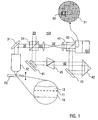
- the wave-front sensing device 100 of the present invention comprises an illumination light path 20, which is split at the beam splitter cube 24 into the sample light path 30 and the reference light path 40.
- the illumination light path 20 includes a laser light source and optical components, which are shown with further details in Fig. 3 .
- the laser light source is a Ti:sapphire laser (Coherent Mira, centre wavelength 915 nm) emitting horizontally polarized light pulses with a pulse duration of about 100 fs.
- the beam splitter cube 24 is a non-polarizing 50:50 splitter (BK 7, Coherent, Inc.).
- the sample light path 30 extends from the beam splitter cube 24 via a deflection mirror 31 and a focussing optic 32 to the specimen 10 and in opposite direction from the specimen 10 via the focussing optic 32, the mirror 31, the beam splitter cube 24, an imaging optic 33 and a beam splitter cube 44 to the detector device 50.
- the deflection mirror 31 is a plane mirror (protected silver, Linos)
- the focussing optic 32 is a microscope objective (Zeiss IR-Acroplan 63 x/0.90W).
- the detector elements 51 are formed by a CCD-Chip (Sony XC-77, pixel dimension about 13 ⁇ m ⁇ 13 ⁇ m). Groups of detector elements 51 represent so called sub-groups 52 to be used for the virtual wave-front sensor (see below). A sub-group 52 of detector elements comprises e.g. 15 * 15 detector elements 51.
- the specimen 10 is positioned with a specimen holding device 70 in the optical axis of the focussing optic 32.
- a specimen holding device 70 any sample carrier or sample table for microscopy can be used which is capable to be shifted at least in a direction parallel to the optical axis of the focussing optic 32 (see double arrow).
- the expanded sectional view of the specimen 10 (bottom of Fig. 1 ) illustrates schematically the irregular shape of the specimen 10 into which the illumination light is focussed to the focal plane 11. Out-of-focus regions 12 in the upper illumination cone of the specimen 10 influence the wave-front of the light travelling through these regions.
- the reference light path 40 extends from the beam splitter cube 24 via a modulator mirror 41, a set of matching prisms 45, a deflection prism 42, a deflection mirror 43 and the beam splitter cube 44 to the detector device 50.
- the modulator mirror 41 comprises a plane mirror (protected silver, Linos) mounted on a piezo actuator (PCL 100-40, Linos).
- the matching prisms 45 comprise 4 glass dispersion matching prisms (60°, BK 7, equilateral prisms, Linos), while the deflection prism 42 is a single right angle prism (BK 7, Linos) for 180° deflection.
- Mirror 43 is a plain mirror (protected silver, Linos).
- the beam splitter cube 44 is a non-polarizing cube (BK 7, Linos).
- the deflection prism 42 is arranged for calibrating the reference path length with regard to the selected sample plane in the specimen to be investigated.
- a reflecting mirror can be positioned in the specimen holding device 70 instead of the specimen.
- the detector device 50 is connected with an evaluation device 60.
- the evaluation device 60 contains a processor portion for reconstructing the wave-front of the sample light on the basis of the phase information obtained from the detector device. Further details of the evaluation device 60 are described with reference to Fig. 3 .
- the wave-front sensing device 100 represents a low coherence interferometer with the focussing optic 32 and the specimen 10 in the sample arm (path 30) and the path length-varying modulator mirror 41 in the reference arm (path 40).
- Coherence gating is achieved by phase-shifting interferometry (PSI), which is described e.g. by P. Carre ""Installation et Utilisation du comperateur photon pulp et interferentiel du Bureau International des Poids et Mesures” in “Metrologia", vol. 2, 1966, p. 13-23 , and by R. Crane, Chapter V. "Interference phase measurement” in "Applied Optics", vol. 8, 1969, p. 538-542 .
- PSI phase-shifting interferometry
- the PSI procedure both rejects wrong path-length light and extracts the phase and thus the wave-front information from the sample light scattered in the focal plane 11 of the specimen 10.
- the interference signal falls of rapidly with arm length mismatch, which leads to a selection volume of about 6 pl and a depth discrimination of about 30 ⁇ m in the focal plane 11. These dimensions represent examples only which are determined by the coherence length of the laser light source.
- the extracted phase can be used to calculate the complex field amplitude in the plane of the detector elements 51.
- a four-step PSI algorithm has been used where quadruplets of images (I1 ... I4) are taken with optical path length differences of 0, ⁇ /4, 2 /4 and 3 /4, respectively.
- each lens of this virtual array is assigned to a sub-group 52 of detector elements 51. From the light intensity measured at each detector element, the phase information and the above complex amplitude is obtained. The complex amplitudes of each sub-group 52 are subjected to a Fourier transformation simulating the optical imaging function of a corresponding lenslet. Phase slope extraction was obtained by fitting the peak position in the focal plane of the virtual lenslets and comparing them to the lenslet centers.
- a scattering phantom comprising 112 nm polystrene beads (Polysciences Inc.) as scatterers embedded in agarose (HMP 2%, Sigma Inc.) at a concentration of about 9.8x10 13 beads/ml.
- the phantom also contained 2.5 ⁇ m diameter fluorescence beads (Molecular Probes) at about 2.1 x 10 7 beads/ml, which were used to measure the mean free path with 2-photon microscopy.
- the focal plane of the focussing optic 32 was positioned approximately 1 mean free path (MFP) below the specimen surface.
- the fraction of the total light passing the coherence gate (CG) and thus being used for wave-front sensing was estimated to be about 1.3 X 10 -3 , using that in the thickness of the coherence gate about 13.2% can be collected (given isotropic scattering) by the solid angle of the objective.
- the attenuation of the incoming and outgoing light (about 63.2% each way) has been taken into account.
- the Lambert-Beer law was used for both scattering and attenuation.
- this fraction was (0.55 ⁇ 0.08)x10 -3 , which is slightly lower than the "Lambert-Beer" value.
- the 'useful' light typically corresponds to 2 ⁇ 0.3 photons per camera pixel and frame, which is considerably below the dark noise of 218 photons but can still be detected, owing to the interferometric detection.
- the illustrated results show that coherence gating of back-scattered light can be used to measure wave-front distortions in scattering samples in the presence of background light that is dominant by about three orders of magnitude.
- the coherence gating technique according to the invention has the additional advantage of increasing the effective sensitivity, with potentially shot-noise limited performance even for low photon fluxes and detectors with large dark noise. This will allow the use of CMOS detector chips, which could in the future contain additional procession circuitry to perform the PSI and even the wave-front calculations on the chip. Detection sensitivity and processing speed will be central for the eventual implementation of closed loop adaptive optics systems for scattering samples.
- Fig. 3 illustrates an embodiment of an imaging device 200 according to the present invention.
- the imaging device (microscope 200) represents the optical setup as shown in Fig. 1 with the illumination light path 20, the sample light path 30 and the reference light path 40.
- the imaging device 200 is adapted for multiphoton microscopy, wherein the specimen scanning is obtained with a movement of the specimen holding device.
- the invention can be implemented correspondingly with a conventional confocal microscope. In this case, further known details like e.g. an optical scanning mechanism, a mechanical scanning mechanism and/or a pinhole diaphragm would be added.
- the illumination light path 20 comprises the laser light source 21, beam forming elements 22 with a pair of imaging lenses 22.1, 22.2 and a deflection mirror 22.3, and a ⁇ /2 plate 23 for controlling the intensity ratio in the sample and reference light paths 30, 40.
- the illumination light is split into the sample light path 30 and the reference light path 40.
- the beam splitter cube 24 is a polarizing cube. The provision of the polarizing beam splitter has the advantage of a high light efficiency. Any lost of light is avoided to the polarization selective splitting.
- the sample light path extends from the beam splitter cube 24 via a ⁇ /4 plate, beam forming elements 31.2 to 31.7, a deformable mirror 34 (OKO Technologies) and the objective 32 to the specimen 10.
- the beam forming elements comprise in particular two pairs of imaging lenses 31.2, 31.3 and 31.5, 31.6, a plane deflection mirror 31.4, and the dichroic beam splitter cube 31.7.
- the deformable mirror 34 is adapted to a predetermined shape in order to form the desired wave-front of the travelling light pulses.
- the objective 32 is the same like the focussing optic shown in Fig. 1 .
- the specimen 10 is arranged on a movable specimen holding device 70.
- the sample light path 30 extends from the specimen 10 via the above mentioned optical components, the polarizing beam splitter cube 24 and the beam splitter cube 44 to the detector device 50, which is connected with the evaluation device 60. Fluorescence light emitted from the specimen 10 can be collected with a photomultiplier 80.
- the reference light path 40 comprises the modulator mirror 41, the deflection prism 42, the deflection mirror 43 and the beam splitter cube 44.
- the evaluation device 60 is illustrated with further details. It contains a simulation circuit 61 being adapted for implementing the wave-front simulation algorithm, in particular the Shack-Hartmann algorithm described above. Furthermore, the evaluation device 60 contains a control circuit 62 which in particular is connected with the deformable mirror 34, the light sensing device 80 and the movable components 41, 42 in the reference light pulse 40.
- the wave-front sensing is obtained with a real array of lenses, e.g. the Shack-Hartmann-Array 53 is arranged in the sample light path 30 between the beam splitting cube 24 and the ⁇ /4 plate 31.1 as shown with dotted lines.
- a real array of lenses e.g. the Shack-Hartmann-Array 53 is arranged in the sample light path 30 between the beam splitting cube 24 and the ⁇ /4 plate 31.1 as shown with dotted lines.
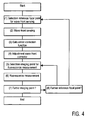
- Fig. 4 illustrates a preferred procedure for microscopic imaging a specimen using the wave-front sensing method according to the invention.
- a first focal point in the focal plane of the specimen is selected for wave-front sensing (step 1).
- the deflection prism 42 in the reference light path is adjusted such that the optical path length from the beam splitter cube 24 through the reference light path 40 to the beam splitter cube 44 is identical with the path length from the beam splitter cube 24 to the focal plane 11 in the specimen (see Fig. 1 ) and back to the beam splitter cube 44.
- the wave-front sensing of the invention is performed (step 2).
- a correction function is calculated (step 3) with the control circuit 62 (see Fig. 3 ).
- the correction function represents a wave-front deformation phase-conjugated to the sensed wave-front.
- the wave-front corrector is adjusted on the basis of the correction function (step 4).
- the microscopic fluorescence measurement is conducted.
- the first focal point is selected for the microscopic imaging.
- This first focal or imaging point may be the first reference focal point selected for wave-front sensing or another focal point in the neighbourhood thereof.
- the fluorescence measurement is performed by exciting the selected imaging point and collecting the fluorescence with the photomultiplier 80.
- a plurality of imaging points are detected. After the decision as to whether a further imaging point is to be detected (step 7), a further decision is made as to whether the illumination of the next imaging point is to be adapted with the wave-front obtained at the first reference focal point or not (step 8). This decision depends on the structure (homogeneity) of the specimen and the extension of the region of interest to be investigated. If a new reference focal point is to be selected, steps 1 to 4 are repeated. Otherwise, the next fluorescence measurement is performed (step 5).
- the present invention can be used for optimizing the focus in optical coherence tomography (high resolution back-scattering) and/or in retina imaging techniques, e.g. for measuring the thickness or any abnormal states in the retina of a human eye.
- the focus for optical reading and/or writing can be improved on the basis of wave-front sensing and illumination adaptation according to the invention. This yields an improvement of optical data storage techniques in terms of storage density.
Landscapes
- Physics & Mathematics (AREA)
- Spectroscopy & Molecular Physics (AREA)
- General Physics & Mathematics (AREA)
- Health & Medical Sciences (AREA)
- Chemical & Material Sciences (AREA)
- Engineering & Computer Science (AREA)
- Biochemistry (AREA)
- General Health & Medical Sciences (AREA)
- Life Sciences & Earth Sciences (AREA)
- Immunology (AREA)
- Pathology (AREA)
- Analytical Chemistry (AREA)
- Computing Systems (AREA)
- Theoretical Computer Science (AREA)
- Nuclear Medicine, Radiotherapy & Molecular Imaging (AREA)
- Microscoopes, Condenser (AREA)
- Investigating, Analyzing Materials By Fluorescence Or Luminescence (AREA)
- Testing Of Optical Devices Or Fibers (AREA)
- Investigating Or Analysing Materials By Optical Means (AREA)
Claims (32)
- Verfahren zur Messung einer Wellenfront von Probenlicht, das aus einem beleuchteten Bereich in einer Probe (10) gestreut wurde, umfassend die Schritte:- Fokussieren von Beleuchtungslicht in die Probe (10), und- Richten von Probenlicht, das in der Probe (10) gestreut wurde, zu einer Detektoreinrichtung (50), die eine Vielzahl von Detektorelementen (51) aufweist und geeignet ist, Licht mit einer Ortsauflösung zu erfassen, und- Detektieren von Abtastlicht, das in dem Probenlicht enthalten ist, mit der Detektoreinrichtung (50), wobei das Abtastlicht in einer vorbestimmten Abtastebene (11) der Probe (10) gestreut worden ist und durch eine zeitbasierte Auftastung des Probenlichts ausgewählt worden ist,gekennzeichnet durch die weiteren Schritte:- örtlich aufgelöstes Messen von Phaseninformation des Abtastlichtes, wobei die Phaseninformation durch die Lichtstreuung in der Probe (10) beeinflusst ist, und- Rekonstruieren der Wellenfront des Abtastlichts auf der Grundlage der Phaseninformation.
- Verfahren gemäß Anspruch 1, wobei die zeitbasierte Austastung des Probenlichts durch eine interferometrische Überlagerung des Probenlichts mit Referenzlicht erhalten wird, das von dem Beleuchtungslicht abgespalten wird.
- Verfahren gemäß Anspruch 2, wobei die Schritte des Detektierens und des Messens der Phaseninformation die Schritte umfassen:- Messen einer Abtastlichtintensität an jedem der Detektorelemente (51), und- Erhalten der Phaseninformation auf der Grundlage der gemessenen Lichtintensitäten.
- Verfahren gemäß Anspruch 3, wobei die Abtastlichtintensitäten, die mit Untergruppen (52) der Detektorelemente (51) gemessen werden, einer Shack-Hartmann-Sensor-Simulation unterzogen werden, die Sub-Apertur-Bilder des Abtastlichts ergeben, wobei die Wellenfront aus den Sub-Apertur-Bildern erhalten wird.
- Verfahren gemäß Anspruch 1 oder 2, wobei die Schritte des Detektierens und Messens der Phaseninformationen die Schritte umfassen:- Transformieren des Probenlichts in eine Vielzahl von Abtastlichtportionen, in dem das Probenlicht einem Wellenfrontsensor ausgesetzt wird, der eine Vielzahl von Portionen des Probenlichts abtastet, das durch eine Apertur der Detektoreinrichtung (50) hindurchtritt,- Bestimmen der Lichtintensitätsverteilungen der Abtastlichtportionen, und- Erhalten der Phaseninformation aus den Lichtintensitätsverteilungen.
- Verfahren gemäß Anspruch 5, wobei der Wellenfrontsensor ein Shack-Hartmann-Array aus Linsen (53) umfasst.
- Verfahren gemäß mindestens einem der vorhergehenden Ansprüche 2 bis 6, wobei die interferometrische Überlagerung des Proben- und des Referenzlichts die Schritte umfasst:- Richten des Referenzlichts durch einen Referenzlichtweg von einer Strahlteilereinrichtung (24) der Detektoreinrichtung (50), wobei der Referenzlichtweg (40) eine optische Referenzweglänge aufweist, die identisch mit einer optischen Abtastweglänge von der Strahlteilereinrichtung (24) über die vorbestimmte Abtastebene (11) der Probe (10) zu der Detektoreinrichtung (50) ist.
- Verfahren gemäß Anspruch 7, umfassend die Schritte:- Modulieren von mindestens einer der optischen Abtast- und Referenzweglängen, um verschiedene Weglängendifferenzen in den Abtast- und Referenzwegen einzustellen,- Wiederholen der Schritte des selektiven Detektierens von Abtastlicht und des Messens von Phaseninformation bei den verschiedenen Weglängendifferenzen, und- Rekonstruieren der Wellenfront des Abtastlichts auf der Grundlage der Phaseninformation, die mit den verschiedenen Weglängendifferenzen erhalten wurde.
- Verfahren gemäß Anspruch 8, wobei die verschiedenen Weglängendifferenzen mindestens drei Werte mit einer gleich beabstandeten Verteilung innerhalb einer Lichtschwingungsperiode umfassen.
- Verfahren gemäß Anspruch 9, wobei die verschiedenen Weglängendifferenzen 0, λ/4, λ/2 and 3λ/4 umfassen, wobei λ die Mittelwellenlänge des Beleuchtungslichts ist.
- Verfahren gemäß mindestens einem der vorhergehenden Ansprüche, wobei der Schritt des Rekonstruierens der Wellenfront des Abtastlichts ein Approximieren der Wellenfront durch einen Satz von orthogonalen Polynomen umfasst.
- Verfahren gemäß Anspruch 11, wobei der Schritt des Rekonstruierens der Wellenfront des Abtastlichts ein Approximieren der Wellenfront durch eine Summe von Zernike-Polynomen umfasst.
- Verfahren gemäß mindestens einem der hervorgehenden Ansprüche, wobei das Abtastlicht in einer Fokalebene (11) der Probe (10) gestreut wird.
- Verfahren des mikroskopischen Abbildens einer Probe, umfassend die Schritte:- Beleuchten von mindestens einem Fokalpunkt der Probe (10) mit adaptiertem Beleuchtungslicht, das eine adaptierte Wellenfront aufweist, die mit einer Wellenfront-Korrektureinrichtung phasenkonjugiert zu einer erfassten Wellenfront gebildet ist, die mit einem Verfahren gemäß mindestens einem der vorhergehenden Ansprüche erhalten wurde, und- Detektieren von Licht, das aus der Probe (10) in Reaktion auf das adaptierte Beleuchtungslicht emittiert wurde.
- Mikroskopisches Abbildungsverfahren gemäß Anspruch 14, wobei die erfasste Wellenfront an dem mindestens einen Fokalpunkt oder in einer Umgebung von dem mindestens einen Fokalpunkt erhalten wird.
- Mikroskopisches Abbildungsverfahren gemäß Anspruch 14 oder 15, wobei die Schritte des Beleuchtens und Detektierens bei einer Vielzahl von Fokalpunkten der Probe (10) wiederholt werden.
- Mikroskopisches Abbildungsverfahren gemäß Anspruch 16, wobei die adaptierte Beleuchtungs-Wellenfront an jedem der Fokalpunkte phasenkonjugiert zu einer gemittelten, erfassten Wellenfront gebildet wird, die an einem benachbarten Punkt oder in einer Umgebung des betreffenden Fokalpunkts erfasst wurde.
- Mikroskopisches Abbildungsverfahren gemäß mindestens einem der Ansprüche 14 bis 17, wobei die Wellenfront-Korrektureinrichtung einen deformierbaren Spiegel (34) oder einen örtlich wirkenden Flüssigkristall-Lichtmodulator umfasst.
- Mikroskopisches Abbildungsverfahren gemäß mindestens einem der Ansprüche 14 bis 18, wobei der Schritt des Detektierens ein Erfassen von Fluoreszenzlicht umfasst, das an dem Fokalpunkt emittiert wird.
- Wellenfront-Messeinrichtung (100) zum Messen einer Wellenfront von Probenlicht, das aus einem beleuchteten Bereich in einer Probe (10) emittiert wird, aufweisend:- eine optische Teilereinrichtung (24), die zur Einführung von Beleuchtungslicht angeordnet ist, und- eine Detektoreinrichtung (50) zum Detektieren von Probenlicht aus der Probe (10), wobei die Detektoreinrichtung (50) eine Vielzahl von Detektorelementen (51) zum Erfassen mit einer Ortsauflösung umfasst, wobei- ein Abtastlichtweg (30) zwischen der optischen Teilereinrichtung (24) und der Detektoreinrichtung (50) gebildet ist und die Probe (10) in dem Abtastlichtweg (30) angeordnet werden kann, so dass das Probenlicht zu der Detektoreinrichtung (50) gerichtet werden kann, und- ein Referenzlichtweg (40) zum zeitbasierten Auswählen von Abtastlicht aus dem Probenlicht gebildet wird, wobei das Abtastlicht in einer vorbestimmten Abtastebene (11) der Probe (10) gestreut wird und das Referenzlicht von dem Beleuchtungslicht an der optischen Teilereinrichtung (24) abgeteilt wird,dadurch gekennzeichnet, dass
die Detektoreinrichtung (50) angeordnet ist, um sowohl Phaseninformation als auch eine komplexe Amplitude des Abtastlichts mit Ortsauflösung zu erhalten, wobei die Phaseninformation durch die Lichtstreuung in der Probe (10) beeinflusst ist,- eine Auswertungseinrichtung (60) mit der Detektoreinrichtung (50) zum Rekonstruieren der Wellenfront des Abtastlichts verbunden ist, und- die Auswertungseinrichtung (60) einen Prozessorbereich zum Rekonstruieren der Wellenfront des Abtastlichts auf der Grundlage der Phaseninformation enthält, die von der Detektoreinrichtung (50) erhalten wird. - Wellenfront-Messeinrichtung gemäß Anspruch 20, wobei mindestens einer von dem Abtastlichtweg (30) und dem Referenzlichtweg (40) eine einstellbare optische Weglänge aufweist.
- Wellenfront-Messeinrichtung gemäß Anspruch 20 oder 21, wobei der Referenzlichtweg (40) für eine interferometrische Überlagerung des Referenzlichts mit dem Probenlicht gebildet ist.
- Wellenfront-Messeinrichtung gemäß mindestens einem der Ansprüche 20 bis 22, wobei die Auswertungseinrichtung (60) einen Simulationsschaltkreis (61) enthält, der Lichtintensitäten, die mit Untergruppen (52) der Detektorelemente (51) erfasst werden, gemäß einer vorbestimmten optischen Abbildungsfunktion verarbeitet.
- Wellenfront-Messeinrichtung gemäß Anspruch 20, wobei der Simulationsschaltkreis (61) zum Simulieren eines Shack-Hartmann-Arrays aus Linsen (53) durch eine Fourier-Transformation der Lichtintensitäten angeordnet ist, die mit den Untergruppen (52) der Detektorelemente (51) erfasst werden.
- Wellenfront-Messeinrichtung gemäß mindestens einem der Ansprüche 20 bis 22, wobei der Abtastlichtweg (40) ein Shack-Hartmann-Array aus Linsen (53) enthält.
- Wellenfront-Messeinrichtung gemäß mindestens einem der Ansprüche 20 bis 25, die ferner einen Modulator (41) umfasst, der zum Modulieren einer Phasenbeziehung zwischen dem Proben- und Referenzlicht angeordnet ist.
- Wellenfront-Messeinrichtung gemäß mindestens einem der Ansprüche 20 bis 26, wobei die Auswertungseinrichtung (60) angepasst ist, um die Wellenfront des Abtastlichts durch einen Satz orthogonaler Polynome zu approximieren.
- Abbildungseinrichtung (200) zum mikroskopischen Abbilden einer Probe, mit:- eine Wellenfront-Messeinrichtung gemäß mindestes einem der Ansprüche 20 bis 27, und- eine Wellenfront-Korrektureinrichtung (34), die in dem Probenlicht (30) angeordnet ist.
- Abbildungseinrichtung gemäß Anspruch 28, wobei die Wellenfront-Korrektureinrichtung einen deformierbaren Spiegel (34) oder einen örtlich wirkenden Flüssigkristall-Lichtmodulator umfasst.
- Abbildungseinrichtung gemäß Anspruch 28 oder 29, wobei die Auswertungseinrichtung (60) einen Steuerschaltkreis (62) enthält, der mit der Wellenfront-Korrektureinrichtung (34) verbunden ist.
- Verfahren der Verwendung einer Abbildungseinrichtung gemäß mindestens einem der Ansprüche 28 bis 30 als ein Konfokalmikroskop oder ein Mehrphoton-Anregungs-Mikroskop.
- Verfahren der Verwendung eines Wellenfront-Messverfahrens gemäß mindestens einem der Ansprüche 1 bis 13 zur Erzeugung von adaptierten Beleuchtungslicht, das eine adaptierte Wellenfront aufweist, um einen Fokus von Beleuchtungslicht zu optimieren, bei:- optischer Kohärenztomographie,- Retina-Abbildungstechniken, und/oder- optischem Lesen oder Schreiben für optische Datenspeicher.
Priority Applications (4)
| Application Number | Priority Date | Filing Date | Title |
|---|---|---|---|
| AT04019068T ATE449319T1 (de) | 2004-08-11 | 2004-08-11 | Verfahren und vorrichtung zur messung von wellenfronten |
| DE602004024193T DE602004024193D1 (de) | 2004-08-11 | 2004-08-11 | Verfahren und Vorrichtung zur Messung von Wellenfronten |
| EP04019068A EP1626257B1 (de) | 2004-08-11 | 2004-08-11 | Verfahren und Vorrichtung zur Messung von Wellenfronten |
| US11/200,457 US7659993B2 (en) | 2004-08-11 | 2005-08-09 | Method and device for wave-front sensing |
Applications Claiming Priority (1)
| Application Number | Priority Date | Filing Date | Title |
|---|---|---|---|
| EP04019068A EP1626257B1 (de) | 2004-08-11 | 2004-08-11 | Verfahren und Vorrichtung zur Messung von Wellenfronten |
Publications (2)
| Publication Number | Publication Date |
|---|---|
| EP1626257A1 EP1626257A1 (de) | 2006-02-15 |
| EP1626257B1 true EP1626257B1 (de) | 2009-11-18 |
Family
ID=34926133
Family Applications (1)
| Application Number | Title | Priority Date | Filing Date |
|---|---|---|---|
| EP04019068A Revoked EP1626257B1 (de) | 2004-08-11 | 2004-08-11 | Verfahren und Vorrichtung zur Messung von Wellenfronten |
Country Status (4)
| Country | Link |
|---|---|
| US (1) | US7659993B2 (de) |
| EP (1) | EP1626257B1 (de) |
| AT (1) | ATE449319T1 (de) |
| DE (1) | DE602004024193D1 (de) |
Families Citing this family (28)
| Publication number | Priority date | Publication date | Assignee | Title |
|---|---|---|---|---|
| US7525666B2 (en) * | 2003-01-20 | 2009-04-28 | Robert Bosch Gmbh | Interferometric measuring device |
| US7840038B2 (en) * | 2006-12-08 | 2010-11-23 | The Invention Science Fund I, Llc | Defect correction based on “virtual” lenslets |
| US8169534B2 (en) * | 2004-02-24 | 2012-05-01 | The Invention Science Fund I, Llc | Volumetric imaging using “virtual” lenslets |
| US7232221B2 (en) * | 2004-02-24 | 2007-06-19 | Searete, Llc | Volumetric imaging using “virtual” lenslets |
| US7220001B2 (en) * | 2004-02-24 | 2007-05-22 | Searete, Llc | Defect correction based on “virtual” lenslets |
| US8198604B2 (en) * | 2007-09-28 | 2012-06-12 | Trustees Of Boston University | System and method for providing enhanced background rejection in thick tissue with differential-aberration two-photon microscopy |
| US20090147269A1 (en) * | 2007-11-05 | 2009-06-11 | Moore Wayne E | Interferometric nanoimaging system |
| KR101022769B1 (ko) * | 2008-10-20 | 2011-03-17 | 삼성전자주식회사 | 바이오칩용 광검출 장치 |
| US8551730B2 (en) * | 2008-10-24 | 2013-10-08 | The Regents Of The University Of California | Use of a reference source with adaptive optics in biological microscopy |
| GB0907277D0 (en) * | 2009-04-29 | 2009-06-10 | Univ Kent Kanterbury | Method for depth resolved wavefront sensing, depth resolved wavefront sensors and method and apparatus for optical imaging |
| JP5336964B2 (ja) * | 2009-07-23 | 2013-11-06 | オリンパス株式会社 | 波面測定装置 |
| JP5642411B2 (ja) * | 2010-03-31 | 2014-12-17 | オリンパス株式会社 | 波面測定方法、波面測定装置および顕微鏡 |
| FR2960291B1 (fr) * | 2010-05-18 | 2015-04-03 | Lltech Man | Methode et dispositif de microscopie interferentielle plein champ a haute resolution |
| CN101929848B (zh) * | 2010-06-30 | 2012-04-25 | 北京理工大学 | 具有高空间分辨力的乘积共焦扫描检测方法 |
| EP2479532A1 (de) | 2011-01-20 | 2012-07-25 | Olympus Corporation | Wellenfrontmessvorrichtung |
| WO2012102887A2 (en) * | 2011-01-24 | 2012-08-02 | The Board Of Trustees Of The University Of Illinois | Computational adaptive optics for interferometric synthetic aperture microscopy and other interferometric imaging |
| DE102012201003A1 (de) * | 2012-01-24 | 2013-07-25 | Carl Zeiss Microscopy Gmbh | Mikroskop und Verfahren für die hochauflösende 3-D Fluoreszenzmikroskopie |
| US9200887B2 (en) | 2012-10-12 | 2015-12-01 | Thorlabs, Inc. | Compact, low dispersion, and low aberration adaptive optics scanning system |
| US9332899B2 (en) * | 2012-11-06 | 2016-05-10 | Clarity Medical Systems, Inc. | Electronic eye marking/registration |
| US9247874B2 (en) | 2013-02-01 | 2016-02-02 | Carl Zeiss Meditec, Inc. | Systems and methods for sub-aperture based aberration measurement and correction in interferometric imaging |
| US9360428B2 (en) | 2013-03-14 | 2016-06-07 | The Regents Of The University Of California | Interferometric focusing of guide-stars for direct wavefront sensing |
| RU2539747C1 (ru) * | 2013-07-26 | 2015-01-27 | Общество с ограниченной ответственностью "ВЕСТТРЭЙД ЛТД" | Фазово-интерференционный модуль |
| EP3250956B1 (de) | 2015-01-26 | 2023-12-27 | Thorlabs, Inc. | Mikroskopiesystem mit autofokuseinstellung durch interferometrie mit niedriger kohärenz |
| US10018817B2 (en) * | 2015-03-04 | 2018-07-10 | Aramco Services Company | Adaptive optics for imaging through highly scattering media in oil reservoir applications |
| US10602925B2 (en) * | 2015-09-11 | 2020-03-31 | Simon Fraser University | Coherence-gated wavefront-sensorless adaptive-optics multi-photon microscopy, and associated systems and methods |
| EP3408646B1 (de) * | 2016-01-28 | 2024-05-29 | Siemens Healthcare Diagnostics Inc. | Verfahren und vorrichtung zur charakterisierung eines probenbehälters und einer probe |
| CN107028590B (zh) * | 2016-12-02 | 2023-06-06 | 北京大学 | 一种微型化自适应光学双光子荧光成像系统及方法 |
| EP3568058A4 (de) * | 2017-01-11 | 2020-11-11 | Avedro, Inc. | Systeme und verfahren zur bestimmung der vernetzungsverteilung in einer hornhaut und/oder strukturmerkmale einer hornhaut |
Family Cites Families (10)
| Publication number | Priority date | Publication date | Assignee | Title |
|---|---|---|---|---|
| US5489984A (en) * | 1994-04-01 | 1996-02-06 | Imra America, Inc. | Differential ranging measurement system and method utilizing ultrashort pulses |
| US5570182A (en) * | 1994-05-27 | 1996-10-29 | Regents Of The University Of California | Method for detection of dental caries and periodontal disease using optical imaging |
| WO2000045153A1 (en) * | 1999-01-29 | 2000-08-03 | June Iris Medford | Optical coherence microscope and methods of use for rapid in vivo three-dimensional visualization of biological function |
| DE10028756B4 (de) * | 2000-06-09 | 2004-05-06 | Forschungsverbund Berlin E.V. | Verfahren und Anordnung zur orts- und zeitaufgelösten interferometrischen Charakterisierung von ultrakurzen Laserimpulsen |
| US6649895B1 (en) * | 2000-07-14 | 2003-11-18 | Adaptive Optics Associates, Inc. | Dispersed Hartmann sensor and method for mirror segment alignment and phasing |
| DE10042751A1 (de) * | 2000-08-31 | 2002-03-14 | Thomas Hellmuth | System zur berührungslosen Vermessung der optischen Abbildungsqualität eines Auges |
| FR2827380B1 (fr) * | 2001-07-12 | 2003-11-07 | Imagine Optic | Dispositif d'analyse d'un front d'onde a resolution amelioree |
| AU2003245458A1 (en) * | 2002-06-12 | 2003-12-31 | Advanced Research And Technology Institute, Inc. | Method and apparatus for improving both lateral and axial resolution in ophthalmoscopy |
| CA2390072C (en) * | 2002-06-28 | 2018-02-27 | Adrian Gh Podoleanu | Optical mapping apparatus with adjustable depth resolution and multiple functionality |
| US7168807B2 (en) * | 2003-06-20 | 2007-01-30 | Visx, Incorporated | Iterative fourier reconstruction for laser surgery and other optical applications |
-
2004
- 2004-08-11 AT AT04019068T patent/ATE449319T1/de not_active IP Right Cessation
- 2004-08-11 DE DE602004024193T patent/DE602004024193D1/de active Active
- 2004-08-11 EP EP04019068A patent/EP1626257B1/de not_active Revoked
-
2005
- 2005-08-09 US US11/200,457 patent/US7659993B2/en not_active Expired - Fee Related
Also Published As
| Publication number | Publication date |
|---|---|
| EP1626257A1 (de) | 2006-02-15 |
| US7659993B2 (en) | 2010-02-09 |
| DE602004024193D1 (de) | 2009-12-31 |
| US20060033933A1 (en) | 2006-02-16 |
| ATE449319T1 (de) | 2009-12-15 |
Similar Documents
| Publication | Publication Date | Title |
|---|---|---|
| US7659993B2 (en) | Method and device for wave-front sensing | |
| US9535247B2 (en) | Interferometric focusing of guide-stars for direct wavefront sensing | |
| JP6460364B2 (ja) | 軸外し反射位相顕微鏡システムおよび軸外し位相顕微鏡のための方法 | |
| Bowman et al. | An SLM-based Shack–Hartmann wavefront sensor for aberration correction in optical tweezers | |
| CN106461925B (zh) | 用于具有自适应光学系统的拉曼散射光学显微镜的系统和方法 | |
| US9411140B2 (en) | Method and system for calibrating a spatial optical modulator in an optical microscope | |
| Beverage et al. | Measurement of the three‐dimensional microscope point spread function using a Shack–Hartmann wavefront sensor | |
| KR102271053B1 (ko) | 수차를 야기하는 샘플 내의 타겟 오브젝트를 이미징하기 위한 초점 스캔 방식의 이미징 장치 | |
| JP2021518576A (ja) | 顕微鏡において光路を操作する方法および装置、顕微鏡においてスタック画像を撮影する方法 | |
| JP7488587B2 (ja) | 対物レンズに対する試料の変位を検出する方法及び装置 | |
| JP7472134B2 (ja) | 試料の3次元領域の蛍光信号を検出するための方法および装置 | |
| Jewel et al. | A direct comparison between a MEMS deformable mirror and a liquid crystal spatial light modulator in signal-based wavefront sensing | |
| Juškaitis | Measuring the real point spread function of high numerical aperture microscope objective lenses | |
| US8009280B1 (en) | Wavefront characterization and correction | |
| Török et al. | Characterizing high numerical aperture microscope objective lenses | |
| Geary | Wavefront sensors | |
| JP2020086204A (ja) | 光画像計測装置、光画像計測方法 | |
| Salmon et al. | High‐resolution video‐enhanced differential interference contrast light microscopy | |
| JP2022523751A (ja) | 階調密度フィルタを使用して光波の表面を検査するためのシステム | |
| Haist et al. | Scene-based wavefront correction with spatial light modulators | |
| Rahman et al. | Adaptive optics for high-resolution microscopy: wave front sensing using back scattered light | |
| Sheppard | Scanned imagery | |
| US20210096349A1 (en) | Imaging device and method for imaging an object using a microscope | |
| US20240168272A1 (en) | Method and device for microscopy | |
| Sensing | Coherence-gated wavefront sensing |
Legal Events
| Date | Code | Title | Description |
|---|---|---|---|
| PUAI | Public reference made under article 153(3) epc to a published international application that has entered the european phase |
Free format text: ORIGINAL CODE: 0009012 |
|
| AK | Designated contracting states |
Kind code of ref document: A1 Designated state(s): AT BE BG CH CY CZ DE DK EE ES FI FR GB GR HU IE IT LI LU MC NL PL PT RO SE SI SK TR |
|
| AX | Request for extension of the european patent |
Extension state: AL HR LT LV MK |
|
| 17P | Request for examination filed |
Effective date: 20060807 |
|
| AKX | Designation fees paid |
Designated state(s): AT BE BG CH CY CZ DE DK EE ES FI FR GB GR HU IE IT LI LU MC NL PL PT RO SE SI SK TR |
|
| 17Q | First examination report despatched |
Effective date: 20071128 |
|
| RAP3 | Party data changed (applicant data changed or rights of an application transferred) |
Owner name: MAX-PLANCK-GESELLSCHAFT ZUR FOERDERUNG DER WISSENS |
|
| GRAP | Despatch of communication of intention to grant a patent |
Free format text: ORIGINAL CODE: EPIDOSNIGR1 |
|
| GRAS | Grant fee paid |
Free format text: ORIGINAL CODE: EPIDOSNIGR3 |
|
| GRAA | (expected) grant |
Free format text: ORIGINAL CODE: 0009210 |
|
| AK | Designated contracting states |
Kind code of ref document: B1 Designated state(s): AT BE BG CH CY CZ DE DK EE ES FI FR GB GR HU IE IT LI LU MC NL PL PT RO SE SI SK TR |
|
| REG | Reference to a national code |
Ref country code: GB Ref legal event code: FG4D |
|
| REG | Reference to a national code |
Ref country code: CH Ref legal event code: EP |
|
| REG | Reference to a national code |
Ref country code: IE Ref legal event code: FG4D |
|
| REF | Corresponds to: |
Ref document number: 602004024193 Country of ref document: DE Date of ref document: 20091231 Kind code of ref document: P |
|
| REG | Reference to a national code |
Ref country code: NL Ref legal event code: VDEP Effective date: 20091118 |
|
| PG25 | Lapsed in a contracting state [announced via postgrant information from national office to epo] |
Ref country code: ES Free format text: LAPSE BECAUSE OF FAILURE TO SUBMIT A TRANSLATION OF THE DESCRIPTION OR TO PAY THE FEE WITHIN THE PRESCRIBED TIME-LIMIT Effective date: 20100228 Ref country code: SE Free format text: LAPSE BECAUSE OF FAILURE TO SUBMIT A TRANSLATION OF THE DESCRIPTION OR TO PAY THE FEE WITHIN THE PRESCRIBED TIME-LIMIT Effective date: 20091118 Ref country code: PT Free format text: LAPSE BECAUSE OF FAILURE TO SUBMIT A TRANSLATION OF THE DESCRIPTION OR TO PAY THE FEE WITHIN THE PRESCRIBED TIME-LIMIT Effective date: 20100318 Ref country code: FI Free format text: LAPSE BECAUSE OF FAILURE TO SUBMIT A TRANSLATION OF THE DESCRIPTION OR TO PAY THE FEE WITHIN THE PRESCRIBED TIME-LIMIT Effective date: 20091118 |
|
| PG25 | Lapsed in a contracting state [announced via postgrant information from national office to epo] |
Ref country code: SI Free format text: LAPSE BECAUSE OF FAILURE TO SUBMIT A TRANSLATION OF THE DESCRIPTION OR TO PAY THE FEE WITHIN THE PRESCRIBED TIME-LIMIT Effective date: 20091118 Ref country code: PL Free format text: LAPSE BECAUSE OF FAILURE TO SUBMIT A TRANSLATION OF THE DESCRIPTION OR TO PAY THE FEE WITHIN THE PRESCRIBED TIME-LIMIT Effective date: 20091118 Ref country code: CY Free format text: LAPSE BECAUSE OF FAILURE TO SUBMIT A TRANSLATION OF THE DESCRIPTION OR TO PAY THE FEE WITHIN THE PRESCRIBED TIME-LIMIT Effective date: 20091118 |
|
| PG25 | Lapsed in a contracting state [announced via postgrant information from national office to epo] |
Ref country code: AT Free format text: LAPSE BECAUSE OF FAILURE TO SUBMIT A TRANSLATION OF THE DESCRIPTION OR TO PAY THE FEE WITHIN THE PRESCRIBED TIME-LIMIT Effective date: 20091118 Ref country code: BE Free format text: LAPSE BECAUSE OF FAILURE TO SUBMIT A TRANSLATION OF THE DESCRIPTION OR TO PAY THE FEE WITHIN THE PRESCRIBED TIME-LIMIT Effective date: 20091118 |
|
| PG25 | Lapsed in a contracting state [announced via postgrant information from national office to epo] |
Ref country code: RO Free format text: LAPSE BECAUSE OF FAILURE TO SUBMIT A TRANSLATION OF THE DESCRIPTION OR TO PAY THE FEE WITHIN THE PRESCRIBED TIME-LIMIT Effective date: 20091118 Ref country code: NL Free format text: LAPSE BECAUSE OF FAILURE TO SUBMIT A TRANSLATION OF THE DESCRIPTION OR TO PAY THE FEE WITHIN THE PRESCRIBED TIME-LIMIT Effective date: 20091118 Ref country code: DK Free format text: LAPSE BECAUSE OF FAILURE TO SUBMIT A TRANSLATION OF THE DESCRIPTION OR TO PAY THE FEE WITHIN THE PRESCRIBED TIME-LIMIT Effective date: 20091118 Ref country code: EE Free format text: LAPSE BECAUSE OF FAILURE TO SUBMIT A TRANSLATION OF THE DESCRIPTION OR TO PAY THE FEE WITHIN THE PRESCRIBED TIME-LIMIT Effective date: 20091118 Ref country code: BG Free format text: LAPSE BECAUSE OF FAILURE TO SUBMIT A TRANSLATION OF THE DESCRIPTION OR TO PAY THE FEE WITHIN THE PRESCRIBED TIME-LIMIT Effective date: 20100218 |
|
| PLBI | Opposition filed |
Free format text: ORIGINAL CODE: 0009260 |
|
| PG25 | Lapsed in a contracting state [announced via postgrant information from national office to epo] |
Ref country code: CZ Free format text: LAPSE BECAUSE OF FAILURE TO SUBMIT A TRANSLATION OF THE DESCRIPTION OR TO PAY THE FEE WITHIN THE PRESCRIBED TIME-LIMIT Effective date: 20091118 Ref country code: SK Free format text: LAPSE BECAUSE OF FAILURE TO SUBMIT A TRANSLATION OF THE DESCRIPTION OR TO PAY THE FEE WITHIN THE PRESCRIBED TIME-LIMIT Effective date: 20091118 |
|
| PLAX | Notice of opposition and request to file observation + time limit sent |
Free format text: ORIGINAL CODE: EPIDOSNOBS2 |
|
| 26 | Opposition filed |
Opponent name: MIZUKAMI, OSAMU Effective date: 20100813 |
|
| PG25 | Lapsed in a contracting state [announced via postgrant information from national office to epo] |
Ref country code: GR Free format text: LAPSE BECAUSE OF FAILURE TO SUBMIT A TRANSLATION OF THE DESCRIPTION OR TO PAY THE FEE WITHIN THE PRESCRIBED TIME-LIMIT Effective date: 20100219 |
|
| PLAF | Information modified related to communication of a notice of opposition and request to file observations + time limit |
Free format text: ORIGINAL CODE: EPIDOSCOBS2 |
|
| PG25 | Lapsed in a contracting state [announced via postgrant information from national office to epo] |
Ref country code: IT Free format text: LAPSE BECAUSE OF FAILURE TO SUBMIT A TRANSLATION OF THE DESCRIPTION OR TO PAY THE FEE WITHIN THE PRESCRIBED TIME-LIMIT Effective date: 20091118 Ref country code: MC Free format text: LAPSE BECAUSE OF NON-PAYMENT OF DUE FEES Effective date: 20100831 |
|
| REG | Reference to a national code |
Ref country code: CH Ref legal event code: PL |
|
| PLBB | Reply of patent proprietor to notice(s) of opposition received |
Free format text: ORIGINAL CODE: EPIDOSNOBS3 |
|
| PG25 | Lapsed in a contracting state [announced via postgrant information from national office to epo] |
Ref country code: CH Free format text: LAPSE BECAUSE OF NON-PAYMENT OF DUE FEES Effective date: 20100831 Ref country code: LI Free format text: LAPSE BECAUSE OF NON-PAYMENT OF DUE FEES Effective date: 20100831 |
|
| PG25 | Lapsed in a contracting state [announced via postgrant information from national office to epo] |
Ref country code: IE Free format text: LAPSE BECAUSE OF NON-PAYMENT OF DUE FEES Effective date: 20100811 |
|
| PG25 | Lapsed in a contracting state [announced via postgrant information from national office to epo] |
Ref country code: HU Free format text: LAPSE BECAUSE OF FAILURE TO SUBMIT A TRANSLATION OF THE DESCRIPTION OR TO PAY THE FEE WITHIN THE PRESCRIBED TIME-LIMIT Effective date: 20100519 Ref country code: LU Free format text: LAPSE BECAUSE OF NON-PAYMENT OF DUE FEES Effective date: 20100811 |
|
| PG25 | Lapsed in a contracting state [announced via postgrant information from national office to epo] |
Ref country code: TR Free format text: LAPSE BECAUSE OF FAILURE TO SUBMIT A TRANSLATION OF THE DESCRIPTION OR TO PAY THE FEE WITHIN THE PRESCRIBED TIME-LIMIT Effective date: 20091118 |
|
| PGFP | Annual fee paid to national office [announced via postgrant information from national office to epo] |
Ref country code: GB Payment date: 20120823 Year of fee payment: 9 |
|
| PGFP | Annual fee paid to national office [announced via postgrant information from national office to epo] |
Ref country code: FR Payment date: 20120831 Year of fee payment: 9 |
|
| PGFP | Annual fee paid to national office [announced via postgrant information from national office to epo] |
Ref country code: DE Payment date: 20121012 Year of fee payment: 9 |
|
| RDAF | Communication despatched that patent is revoked |
Free format text: ORIGINAL CODE: EPIDOSNREV1 |
|
| REG | Reference to a national code |
Ref country code: DE Ref legal event code: R103 Ref document number: 602004024193 Country of ref document: DE Ref country code: DE Ref legal event code: R064 Ref document number: 602004024193 Country of ref document: DE |
|
| RDAG | Patent revoked |
Free format text: ORIGINAL CODE: 0009271 |
|
| STAA | Information on the status of an ep patent application or granted ep patent |
Free format text: STATUS: PATENT REVOKED |
|
| 27W | Patent revoked |
Effective date: 20130503 |
|
| GBPR | Gb: patent revoked under art. 102 of the ep convention designating the uk as contracting state |
Effective date: 20130503 |
|
| REG | Reference to a national code |
Ref country code: DE Ref legal event code: R107 Ref document number: 602004024193 Country of ref document: DE Effective date: 20131031 |