EP1610261B1 - Chipmodule for a portable data carrier - Google Patents
Chipmodule for a portable data carrier Download PDFInfo
- Publication number
- EP1610261B1 EP1610261B1 EP20050012874 EP05012874A EP1610261B1 EP 1610261 B1 EP1610261 B1 EP 1610261B1 EP 20050012874 EP20050012874 EP 20050012874 EP 05012874 A EP05012874 A EP 05012874A EP 1610261 B1 EP1610261 B1 EP 1610261B1
- Authority
- EP
- European Patent Office
- Prior art keywords
- chip module
- integrated circuit
- portable data
- carrier
- card body
- Prior art date
- Legal status (The legal status is an assumption and is not a legal conclusion. Google has not performed a legal analysis and makes no representation as to the accuracy of the status listed.)
- Active
Links
Images

Classifications
-
- G—PHYSICS
- G06—COMPUTING; CALCULATING OR COUNTING
- G06K—GRAPHICAL DATA READING; PRESENTATION OF DATA; RECORD CARRIERS; HANDLING RECORD CARRIERS
- G06K19/00—Record carriers for use with machines and with at least a part designed to carry digital markings
- G06K19/06—Record carriers for use with machines and with at least a part designed to carry digital markings characterised by the kind of the digital marking, e.g. shape, nature, code
- G06K19/067—Record carriers with conductive marks, printed circuits or semiconductor circuit elements, e.g. credit or identity cards also with resonating or responding marks without active components
- G06K19/07—Record carriers with conductive marks, printed circuits or semiconductor circuit elements, e.g. credit or identity cards also with resonating or responding marks without active components with integrated circuit chips
- G06K19/077—Constructional details, e.g. mounting of circuits in the carrier
- G06K19/07745—Mounting details of integrated circuit chips
- G06K19/07747—Mounting details of integrated circuit chips at least one of the integrated circuit chips being mounted as a module
-
- H—ELECTRICITY
- H01—ELECTRIC ELEMENTS
- H01L—SEMICONDUCTOR DEVICES NOT COVERED BY CLASS H10
- H01L2924/00—Indexing scheme for arrangements or methods for connecting or disconnecting semiconductor or solid-state bodies as covered by H01L24/00
- H01L2924/0001—Technical content checked by a classifier
- H01L2924/0002—Not covered by any one of groups H01L24/00, H01L24/00 and H01L2224/00
Description
Die Erfindung betrifft ein Chipmodul für einen tragbaren Datenträger. Weiterhin betrifft die Erfindung einen mit einem derartigen Chipmodul ausgestatteten tragbaren Datenträger.The invention relates to a chip module for a portable data carrier. Furthermore, the invention relates to a portable data carrier equipped with such a chip module.
Kartenförmige Datenträger, insbesondere Chipkarten werden in vielen Bereichen eingesetzt, beispielsweise als Ausweisdokumente, zum Nachweis einer Zugangsberechtigung zu einem Mobilfunknetz oder im öffentlichen Nahverkehr sowie zur Durchführung von Transaktionen des bargeldlosen Zahlungsverkehrs. Eine Chipkarte weist einen Kartenkörper und einen in den Kartenkörper eingebetteten integrierten Schaltkreis auf. Um eine effiziente Herstellung der Chipkarte zu ermöglichen, wird der integrierte Schaltkreis bei einer Vielzahl von Herstellungsverfahren zunächst in ein Chipmodul verpackt und anschließend das Chipmodul in den Kartenkörper eingebaut. Insbesondere wird das Chipmodul in eine Aussparung des Kartenkörpers eingeklebt.Card-shaped data carriers, in particular chip cards, are used in many areas, for example as identity documents, as proof of access authorization to a mobile radio network or in public transport, and for carrying out transactions of cashless payment transactions. A smart card has a card body and an integrated circuit embedded in the card body. In order to enable efficient production of the chip card, the integrated circuit is initially packaged in a chip module in a large number of production methods, and then the chip module is installed in the card body. In particular, the chip module is glued into a recess of the card body.
Eine Kommunikation mit dem integrierten Schaltkreis kann über ein Kontaktfeld der Chipkarte abgewickelt werden, das hierzu von einer Kontaktiereinheit berührend kontaktiert wird. Das Kontaktfeld ist in der Regel Bestandteil des Chipmoduls. Alternativ oder zusätzlich zur Kommunikation über das Kontaktfeld kann eine kontaktlose Kommunikation vorgesehen sein. Hierzu kann der Kartenkörper eine Antenne aufweisen, die beim Einbau des Chipmoduls elektrisch leitend mit dem integrierten Schaltkreis verbunden wird. Außerdem können beim Einbau des Chipmoduls in den Kartenkörper elektrisch leitende Verbindungen zu weiteren elektrischen Komponenten des Kartenkörpers hergestellt werden. Dies ist allerdings insofern schwierig, da durch die dafür erforderlichen Anschlüsse die Klebefläche zwischen dem Chipmodul und dem Kartenkörper reduziert wird und somit die Zahl bzw. Größe der Anschlüsse wegen des erforderlichen Verbunds zwischen dem Chipmodul und dem Kartenkörper sehr limitiert ist.Communication with the integrated circuit can be carried out via a contact field of the chip card, which is contacted by a contacting unit for this purpose. The contact field is usually part of the chip module. Alternatively or in addition to the communication via the contact field, a contactless communication may be provided. For this purpose, the card body may have an antenna, which is electrically connected to the integrated circuit during installation of the chip module. In addition, electrically conductive connections can be made to other electrical components of the card body during installation of the chip module in the card body. However, this is difficult insofar as the adhesive area between the chip module and the card body is reduced by the connections required for this purpose and thus the number or size of the connections is very limited because of the required interconnection between the chip module and the card body.
Beispielsweise aus der
Der Erfindung liegt die Aufgabe zugrunde, ein Chipmodul für einen tragbaren Datenträger so auszubilden, dass ausreichend Anschlussmöglichkeiten für elektrische Komponenten bestehen und zudem ein stabiler Verbund zwischen dem Chipmodul und dem Kartenkörper möglich ist.The invention has the object of providing a chip module for a portable data carrier in such a way that there are sufficient connection options for electrical components and also a stable bond between the chip module and the card body is possible.
Diese Aufgabe wird durch ein Chipmodul mit der Merkmalskombination des Anspruchs 1 gelöst.This object is achieved by a chip module with the feature combination of
Das erfindungsgemäße Chipmodul für einen tragbaren Datenträger weist einen integrierten Schaltkreis auf, der auf einem Träger angeordnet ist. Die Besonderheit des erfindungsgemäßen Chipmoduls besteht darin, dass auf dem Träger in einem seitlichen Abstand zum integrierten Schaltkreis ein Anschlussfeld mit mehreren Anschlüssen zum Anschließen wenigstens einer elektrischen Komponente des tragbaren Datenträgers ausgebildet ist, wobei das Anschlussfeld außerhalb eines Klebebereichs angeordnet ist und wobei der Klebebereich in einer Aussparung des Datenträgers angeordnet ist. Dabei umgibt der Klebebereich den integrierten Schaltkreis oder einen Vergusskörper, in den der integrierte Schaltkreis eingebettet ist und dient der Fixierung am tragbaren Datenträger.The chip module for a portable data carrier according to the invention has an integrated circuit which is arranged on a carrier. The peculiarity of the chip module according to the invention is that on the carrier in a lateral distance from the integrated circuit, a terminal panel is formed with a plurality of terminals for connecting at least one electrical component of the portable data carrier, wherein the connection pad is disposed outside of an adhesive region and wherein the adhesive area in a Recess of the data carrier is arranged. The adhesive area surrounds the integrated circuit or a potting, in which the integrated circuit is embedded and serves to fix the portable data carrier.
Die Erfindung hat den Vorteil, dass auf dem Chipmodul ausreichend Anschlussmöglichkeiten für elektrische Komponenten bestehen und zudem ein zuverlässiger Verbund zwischen dem Chipmodul und dem Kartenkörper möglich ist. Ein weiterer Vorteil besteht darin, dass das Anschlussfeld in einem Bereich angeordnet ist, in dem nach dem Einbau des Chipmoduls in den Kartenkörper keine allzu hohen mechanischen Belastungen auftreten und dadurch die mittels des Anschlussfeldes ausgebildeten elektrischen Verbindungen sehr stabil sind.The invention has the advantage that there are sufficient connection possibilities for electrical components on the chip module and, moreover, a reliable connection between the chip module and the card body is possible. A further advantage consists in that the connection field is arranged in a region in which after installation of the chip module in the card body no excessively high mechanical loads occur and thereby the electrical connections formed by means of the connection field are very stable.
In einem bevorzugten Ausführungsbeispiel des erfindungsgemäßen Chipmoduls ist der integrierte Schaltkreis in einen Vergusskörper eingebettet und das Anschlussfeld außerhalb des Vergusskörpers, vorzugsweise in einem seitlichen Abstand von mindestens 2mm zum Vergusskörper, angeordnet.In a preferred embodiment of the chip module according to the invention, the integrated circuit is embedded in a potting body and the connection field outside the potting, preferably in a lateral distance of at least 2mm to the potting arranged.
Besonders vorteilhaft ist es, wenn das Anschlussfeld außerhalb eines Klebebereichs angeordnet ist, der den integrierten Schaltkreis oder den Vergusskörper umgibt und der Fixierung am tragbaren Datenträger dient. Auf diese Weise kann eine Beeinträchtigung des Verbunds zwischen dem Chipmodul und dem Kartenkörper durch das Anschlussfeld ausgeschlossen werden.It is particularly advantageous if the connection field is arranged outside of an adhesive area which surrounds the integrated circuit or the potting body and serves for fixing to the portable data carrier. In this way, an impairment of the bond between the chip module and the card body can be excluded by the connection field.
Wenigstens einige der Anschlüsse können mit dem integrierten Schaltkreis elektrisch leitend verbunden sein. Weiterhin kann vorgesehen sein, dass wenigstens einige der Anschlüsse auf derselben Hauptfläche des Trägers angeordnet sind, auf der auch der integrierte Schaltkreis angeordnet ist.At least some of the terminals may be electrically connected to the integrated circuit. Furthermore, it can be provided that at least some of the terminals are arranged on the same main surface of the carrier, on which the integrated circuit is also arranged.
Im Bereich des Anschlussfeldes kann wenigstens ein kapazitives und/oder wenigstens ein induktives Element ausgebildet sein. Ebenso ist es möglich, dass im Bereich des Anschlussfeldes wenigstens eine Schalteinrichtung ausgebildet ist. Weiterhin kann im Bereich des Anschlussfeldes wenigstens ein elektronisches Bauteil, vorzugsweise in SMD-Technik, angeordnet sein. Auf diese Weise kann das Anschlussfeld sehr vielfältig genutzt werden.At least one capacitive and / or at least one inductive element can be formed in the region of the connection field. It is also possible that at least one switching device is formed in the region of the connection field. Furthermore, at least one electronic component, preferably in SMD technology, can be arranged in the region of the connection field. In this way, the connection field can be used very varied.
Der integrierte Schaltkreis kann mit einem standardisierten Kontaktfeld für eine externe Kontaktierung elektrisch leitend verbunden sein. Dabei kann das Anschlussfeld seitlich versetzt zum Kontaktfeld für die externe Kontaktierung angeordnet sein.The integrated circuit may be electrically connected to a standardized contact pad for external contacting. In this case, the connection field can be arranged laterally offset from the contact field for external contacting.
Der erfindungsgemäße tragbare Datenträger weist einen Kartenkörper mit wenigstens einer elektrischen Komponente auf. Weiterhin ist ein Chipmodul mit einem auf einem Träger angeordneten integrierten Schaltkreis vorgesehen, das ganz oder teilweise in den Kartenkörper eingebettet ist und elektrisch leitend mit der elektrischen Komponente des Kartenkörpers verbunden ist. Die Besonderheit des erfindungsgemäßen tragbaren Datenträgers besteht darin, dass die elektrisch leitende Verbindung zwischen dem Chipmodul und der elektrischen Komponente des Kartenkörpers mittels eines Anschlussfeldes des Chipmoduls realisiert ist, das in einem seitlichen Abstand zum integrierten Schaltkreis auf dem Träger ausgebildet ist und mehrere Anschlüsse aufweist.The portable data carrier according to the invention has a card body with at least one electrical component. Furthermore, a chip module is provided with an integrated circuit arranged on a carrier, which is completely or partially embedded in the card body and is electrically connected to the electrical component of the card body. The peculiarity of the portable data carrier according to the invention is that the electrically conductive connection between the chip module and the electrical component of the card body is realized by means of a connection pad of the chip module, which is formed at a lateral distance from the integrated circuit on the carrier and has a plurality of terminals.
Besonders vorteilhaft ist es, wenn wenigstens einige Anschlüsse des Anschlussfeldes mittels eines elektrisch leitenden Klebers, der vorzugsweise eine anisotrope Leitfähigkeit aufweist, elektrisch leitend mit dafür vorgesehenen Strukturen des Kartenkörpers verbunden sind. Eine derart ausgebildete elektrisch leitende Verbindung lässt sich mit einem vergleichsweise geringen Aufwand herstellen.It is particularly advantageous if at least some terminals of the connection field are electrically conductively connected to structures of the card body provided for this purpose by means of an electrically conductive adhesive, which preferably has an anisotropic conductivity. Such a trained electrically conductive connection can be produced with a relatively low cost.
In einer Weiterbildung des erfindungsgemäßen tragbaren Datenträgers ist wenigstens ein Anschluss des Anschlussfeldes außerhalb des Kartenkörpers zugänglich. Dieser Anschluss kann für eine Kontaktierung durch ein externes Gerät genutzt werden.In one development of the portable data carrier according to the invention, at least one connection of the connection field outside the card body is accessible. This connection can be used for contacting by an external device.
Der erfindungsgemäße tragbare Datenträger ist vorzugsweise so ausgebildet, dass die lateralen Abmessungen des Chipmoduls kleiner sind als die lateralen Abmessungen des Kartenkörpers. Das Chipmodul kann in einer vorzugsweise zweistufig ausgebildeten Aussparung des Kartenkörpers angeordnet sein, die zur Umgebung hin offen ist. Dadurch ist gewährleistet, dass für die Herstellung des Chipmoduls und des Kartenkörpers bekannte Herstellungsverfahren eingesetzt werden können.The portable data carrier according to the invention is preferably designed such that the lateral dimensions of the chip module are smaller than the lateral dimensions of the card body. The chip module may be arranged in a preferably two-step recess of the card body, which is open to the environment. This ensures that known production methods can be used for the production of the chip module and the card body.
Die Erfindung wird nachstehend anhand der in der Zeichnung dargestellten Ausführungsbeispiele erläutert.The invention will be explained below with reference to the embodiments illustrated in the drawings.
Es zeigen:
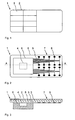
- Fig.
- 1 eine Aufsicht auf die Vorderseite eines Ausführungsbeispiels eines erfindungsgemäß ausgebildeten Chipmoduls,
- Fig. 2
- eine Aufsicht auf die Rückseite des in
Fig. 1 dargestellten Ausführungsbeispiels des erfindungsgemäßen Chipmoduls, - Fig. 3
- eine Schnittdarstellung des in den
Fig. 1 und 2 dargestellten Ausführungsbeispiels des erfindungsgemäßen Chipmoduls, - Fig. 4
- eine weitere Aufsicht auf die Rückseite des in den
Fig. 1 bis 3 dargestellten Ausführungsbeispiels des erfindungsgemäßen Chipmoduls, - Fig. 5
- eine Schnittdarstellung eines Ausführungsbeispiels der erfindungsgemäßen Chipkarte mit dem in den
Fig. 1 bis 4 dargestellten Chipmodul und - Fig. 6
- eine Aufsicht auf die Rückseite eines weiteren Ausführungsbeispiels des erfindungsgemäßen Chipmoduls.
- FIG.
- 1 shows a plan view of the front side of an exemplary embodiment of a chip module designed according to the invention,
- Fig. 2
- a top view on the back of the in
Fig. 1 illustrated embodiment of the chip module according to the invention, - Fig. 3
- a sectional view of the in the
Fig. 1 and 2 illustrated embodiment of the chip module according to the invention, - Fig. 4
- another overhead view of the back of the
Fig. 1 to 3 illustrated embodiment of the chip module according to the invention, - Fig. 5
- a sectional view of an embodiment of the smart card according to the invention with the in the
Fig. 1 to 4 represented chip module and - Fig. 6
- a plan view of the back of another embodiment of the chip module according to the invention.
Das Chipmodul 1 ist für den Einbau in eine Chipkarte vorgesehen und weist auf seiner Vorderseite, die nach dem Einbau des Chipmoduls 1 nach außen gerichtet ist, ein Kontaktfeld 2 auf. Das Kontaktfeld 2 kann gemäß der Norm ISO/IEC 7816 ausgebildet sein und besteht aus einer Reihe von Kontaktflächen 3, die mittels einer nicht figürlich dargestellten Kontaktiereinheit eines externen Geräts berührend kontaktiert werden können.The
Auf seiner in
In einer Weiterbildung des in
Alternativ dazu kann zur Herstellung elektrisch leitender Verbindungen zwischen den Leiterbahnen 10 der Chipkarte und den Anschlüssen 8 des Chipmoduls 1 beispielsweise auch die Flexible Bump Methode eingesetzt werden, bei der die Anschlüsse 8 des Chipmoduls 1 direkt an den Leiterbahnen 10 der Chipkarte anliegen und mit diesen verlötet oder verschweißt werden.Alternatively, for the production of electrically conductive connections between the conductor tracks 10 of the chip card and the
Durch die Anordnung des Anschlussfeldes 7 des Chipmoduls 1 in einem Abstand zum Vergusskörper 6 kann die mechanische Belastung des Anschlussfeldes 7, beispielsweise bei einer Biegebeanspruchung des Kartenkörpers 11, relativ gering gehalten werden, da eine räumliche Trennung vom versteifend wirkenden Vergusskörper 6 vorliegt.The arrangement of the
In einer Abwandlung des dargestellten Ausführungsbeispiels ist es vorgesehen, dass wenigstens einige Anschlüsse 8 des Anschlussfeldes 7 von außerhalb der Chipkarte zugänglich sind. Dies kann beispielsweise dadurch erreicht werden, dass diese Anschlüsse 8 auf der Vorderseite des Chipmoduls 1 angeordnet werden. Die von außen zugänglichen Anschlüsse 8 können ähnlich wie das Kontaktfeld 2 von einer Kontaktiereinheit eines externen Geräts kontaktiert werden. Auf diese Weise kann beispielsweise eine im Kartenkörper 11 angeordnete Batterie aufgeladen werden. Ebenso ist es auch möglich, dass auf der Vorderseite des Chipmoduls 1 angeordnete Anschlüsse 8 als Sensortaster genutzt werden. Diese Anschlüsse 8 können mit Leiterbahnen 9 des Chipmoduls 1 oder mit Leiterbahnen 10 der Chipkarte verbunden sein und beispielsweise dazu dienen, Funktionen der Chipkarte zu schalten.In a modification of the illustrated embodiment, it is provided that at least some
In einer weiteren Abwandlung weist das Anschlussfeld 7 zusätzlich oder alternativ zu den Anschlüssen 8 weitere Komponenten auf. Dies ist in
Auf der Rückseite des Chipmoduls 1 können zusätzlich zur Antenne 14 Anschlüsse 8 vorhanden sein, die allerdings in
Ebenso ist es auch möglich, die Antenne 14 auf der Vorderseite des Chipmoduls 1 anzuordnen und die Rückseite des Chipmoduls 1 entsprechend
Ebenso können im Bereich des Anschlussfeldes 7 elektronische Bauteile, insbesondere in SMD-Technik, aufgebracht werden. Im Bereich des Anschlussfeldes kann eine ebenfalls nicht dargestellte Schalteinrichtung ausgebildet sein. Die Schalteinrichtung ist vorzugsweise aussenseitig, also auf der in
Der Erfindungsgedanke kann auf eine Anordnung einer Antenne auf einem Träger angewandt werden. Die Antenne ist dann in einem seitlichen Abstand zum integrierten Schaltkreis 4 auf dem Träger 5 angeordnet, ohne daß ein Anschlußfeld vorliegt. Die weiteren oben genannten erfindungsgemäßen Aspekte einer Anordnung eines Anschlussfeldes sind ebenso auf die Anordnung einer Antenne anwendbar.The inventive concept can be applied to an arrangement of an antenna on a carrier. The antenna is then arranged at a lateral distance from the
Zusätzlich oder alternativ zu den bereits beschriebenen Varianten sind für das Chipmodul 1 eine Reihe von weiteren Abwandlungen und Weiterbildungen möglich. So können beim Chipmodul 1 beispielsweise auch mehrere Anschlussfelder 7 vorgesehen sein, insbesondere zwei Anschlussfelder 7 auf einander gegenüberliegenden Seiten des integrierten Schaltkreises 4. Das Chipmodul 1 kann auch bezüglich seines Grundaufbaus andersartig ausgebildet sein. Dabei können prinzipiell beliebige Standardverfahren der Chipmodulherstellung eingesetzt werden, beispielsweise die Lead Frame Technik, bei welcher der integrierte Schaltkreis 4 auf einem ausgestanzten Kontaktfeld 2 angeordnet wird, die Flip Chip Technik, bei welcher der integrierte Schaltkreis 4 mit seiner Kontaktseite auf der Trägerfolie 5 angeordnet wird usw.In addition or as an alternative to the variants already described, a number of further modifications and developments are possible for the
Die erfindungsgemäße Chipkarte kann je nach Anwendungsbereich für eine Kommunikation über eine berührende Kontaktierung oder eine kontaktlose Kommunikation ausgelegt werden. Ebenso ist es auch möglich, dass die Chipkarte sowohl über eine berührende Kontaktierung als auch kontaktlos kommunizieren kann.Depending on the field of application, the chip card according to the invention can be designed for communication via a contacting contact or a contactless communication. Likewise, it is also possible that the chip card can communicate both via a contacting contact and contactless.
Ein tragbarer Datenträger im Sinne der vorliegenden Erfidnung ist insbesondere ein kartenförmiger Datenträger, beispielsweise eine Chipkarte oder ein SIM-Modul, ein Token, beispielsweise ein USB-Token, oder auch ein Schlüsselanhänger.A portable data carrier in the sense of the present invention is in particular a card-shaped data carrier, for example a chip card or a SIM module, a token, for example a USB token, or else a key fob.
Claims (13)
- A chip module for a portable data carrier, having an integrated circuit (4) arranged on a carrier (5) characterized in that on the carrier (5) there is configured at a lateral distance to the integrated circuit (4) a connector pad (7) with several connectors (8) for connecting at least one electric component, wherein the connector pad (7) is arranged outside a region of the carrier foil (5) surrounding the cast body, and wherein the region of the carrier foil (5) surrounding the cast body surrounds the integrated circuit (4) or a cast body (6) in which the integrated circuit (4) is embedded.
- The chip module according to any of the preceding claims, characterized in that at least some of the connectors (8) are connected electroconductively with the integrated circuit (4).
- The chip module according to any of the preceding claims, characterized in that at least some of the connectors (8) are arranged on the same main area of the carrier (5) on which also the integrated circuit (4) is arranged.
- The chip module according to any of the preceding claims, characterized in that in the region of the connector pad (7) at least one capacitive and/ or at least one inductive element (14) is configured.
- The chip module according to any of the preceding claims, characterized in that in the region of the connector pad (7) at least one switching device is configured.
- The chip module according to any of the preceding claims, characterized in that in the region of the connector pad (7) at least one electronic component, preferably in SMD technology, is arranged.
- The chip module according to any of the preceding claims, characterized in that the integrated circuit (4) is connected electroconductively with a standardized contact pad (2) for external contacting.
- The chip module according to claim 7, characterized in that the connector pad (7) is arranged laterally offset from the contact pad (2) for the external contacting.
- A portable data carrier with a card body (11) having at least one electric component, and a chip module (1) according to claim 1, characterized in that the electroconductive connection between the chip module (1) and the electric component of the card body (11) is realized by means of a connector pad (7) of the chip module (1) that is configured on the carrier (5) at a lateral distance to the integrated circuit (4) and has several connectors (8).
- The portable data carrier according to claim 9, characterized in that at least some connectors (8) of the connector pad (7) are connected electroconductively with structures (10) of the card body (11) provided for this purpose by means of an electroconductive adhesive (13) preferably having an anisotropic conductivity.
- The portable data carrier according to any of the claims 9 or 10, characterized in that at least one connector (8) of the connector pad (7) is accessible outside the card body (11).
- The portable data carrier according to any of the claims 9 to 11, characterized in that the lateral dimensions of the chip module (1) are smaller than the lateral dimensions of the card body (11).
- The portable data carrier according to any of the claims 9 to 12, characterized in that the chip module (1) is arranged in a recess (12) of the card body (11), said recess being preferably of a two-step configuration and being open towards the surroundings.
Applications Claiming Priority (2)
| Application Number | Priority Date | Filing Date | Title |
|---|---|---|---|
| DE200410030749 DE102004030749A1 (en) | 2004-06-25 | 2004-06-25 | Chip module for a portable data carrier |
| DE102004030749 | 2004-06-25 |
Publications (2)
| Publication Number | Publication Date |
|---|---|
| EP1610261A1 EP1610261A1 (en) | 2005-12-28 |
| EP1610261B1 true EP1610261B1 (en) | 2013-03-27 |
Family
ID=34937467
Family Applications (1)
| Application Number | Title | Priority Date | Filing Date |
|---|---|---|---|
| EP20050012874 Active EP1610261B1 (en) | 2004-06-25 | 2005-06-15 | Chipmodule for a portable data carrier |
Country Status (3)
| Country | Link |
|---|---|
| EP (1) | EP1610261B1 (en) |
| DE (1) | DE102004030749A1 (en) |
| ES (1) | ES2405263T3 (en) |
Families Citing this family (2)
| Publication number | Priority date | Publication date | Assignee | Title |
|---|---|---|---|---|
| WO2008081224A1 (en) * | 2006-12-28 | 2008-07-10 | Fci | Flat substrates for identification cards and manufacturing methods of the same |
| DE102007054385A1 (en) * | 2007-11-14 | 2009-05-20 | Giesecke & Devrient Gmbh | Create a portable volume |
Family Cites Families (7)
| Publication number | Priority date | Publication date | Assignee | Title |
|---|---|---|---|---|
| FR2634095A1 (en) * | 1988-07-05 | 1990-01-12 | Bull Cp8 | Flexible printed circuit, especially for a card having electronic microcircuits, and card incorporating such a circuit |
| DE19500925C2 (en) * | 1995-01-16 | 1999-04-08 | Orga Kartensysteme Gmbh | Method for producing a contactless chip card |
| DE19721281C2 (en) * | 1997-05-21 | 1999-04-01 | Ods Landis & Gyr Gmbh & Co Kg | Chip module for a chip card |
| FR2780848A1 (en) * | 1998-07-06 | 2000-01-07 | Solaic Sa | ANTENNA WITH SLOTTED CONNECTION TERMINALS FOR INTEGRATED CIRCUIT BOARD, AND INTEGRATED CIRCUIT BOARD INCLUDING SUCH ANTENNA |
| DE19955538B4 (en) * | 1999-11-18 | 2014-06-05 | Morpho Cards Gmbh | Printed conductor carrier layer for lamination into a chip card, method for producing a conductor carrier layer Injection molding tool for carrying out the method for producing a conductor carrier layer |
| DE10019431A1 (en) * | 2000-04-19 | 2001-10-25 | Power Digital Card Co | Multimedia card production method involves forming conducting carrier or conducting bracket and card integrally by injection molding |
| DE10120254A1 (en) | 2001-04-25 | 2002-11-07 | Infineon Technologies Ag | Smart card module |
-
2004
- 2004-06-25 DE DE200410030749 patent/DE102004030749A1/en not_active Withdrawn
-
2005
- 2005-06-15 EP EP20050012874 patent/EP1610261B1/en active Active
- 2005-06-15 ES ES05012874T patent/ES2405263T3/en active Active
Also Published As
| Publication number | Publication date |
|---|---|
| EP1610261A1 (en) | 2005-12-28 |
| DE102004030749A1 (en) | 2006-01-19 |
| ES2405263T3 (en) | 2013-05-30 |
Similar Documents
| Publication | Publication Date | Title |
|---|---|---|
| EP0886834B1 (en) | Smart card and process for manufacturing a smart card | |
| EP1429283B1 (en) | Portable data carrier | |
| EP1152368B1 (en) | Chip card | |
| EP1553663B1 (en) | Contact unit for card-shaped carriers with electronic components | |
| EP1816583B1 (en) | Contact device for a chip card | |
| DE19940695B4 (en) | Electronic media device | |
| EP0996932B1 (en) | Data carrier which can be operated without contact | |
| WO1998028709A1 (en) | Non-conductive substrate forming a band or panel, on which are formed a plurality of support elements | |
| DE102020108927A1 (en) | Sensor device, method for forming a sensor device, carrier tape, chip card and method for forming a chip card | |
| EP1610261B1 (en) | Chipmodule for a portable data carrier | |
| DE102005030794B4 (en) | Electronic device with a security module | |
| EP2700055B1 (en) | Id signal transmitter for a motor vehicle access system with a removable nfc assembly | |
| DE102010028868B4 (en) | Semiconductor substrate-based arrangement for an RFID device, RFID device and method for producing such a semiconductor substrate-based arrangement | |
| DE10108080C1 (en) | Contactless data carrier with capacitively coupled antenna coil has spacer elements between IC substrate contacts and cooperating coil terminals | |
| DE102007022615A1 (en) | Contactless transmission system and method of making the same | |
| EP1695454B1 (en) | Electronic device provided with a security module | |
| EP1684216A1 (en) | Portable data carrier | |
| EP1352362B1 (en) | Data carrier arrangement with a display device | |
| EP1668571B1 (en) | Portable data carrier | |
| EP1472650B1 (en) | Foil battery with integrated component for use in a chip card | |
| DE102005002728A1 (en) | Portable data carrier e.g. smart card, for e.g. mobile network, has grouting body with channels that extend upto integrated circuit contacts and inserted in conducting adhesive subsequent to formation of electrical conductive connection | |
| DE19612718B4 (en) | Chip card with battery and method for mounting a chip module / battery unit | |
| DE102005002733B4 (en) | Portable data carrier | |
| WO1998033143A1 (en) | Support element to be inserted into chipcards, and the chipcard for receiving same | |
| EP2290590B1 (en) | Portable data carrier |
Legal Events
| Date | Code | Title | Description |
|---|---|---|---|
| PUAI | Public reference made under article 153(3) epc to a published international application that has entered the european phase |
Free format text: ORIGINAL CODE: 0009012 |
|
| AK | Designated contracting states |
Kind code of ref document: A1 Designated state(s): AT BE BG CH CY CZ DE DK EE ES FI FR GB GR HU IE IS IT LI LT LU MC NL PL PT RO SE SI SK TR |
|
| AX | Request for extension of the european patent |
Extension state: AL BA HR LV MK YU |
|
| 17P | Request for examination filed |
Effective date: 20060628 |
|
| AKX | Designation fees paid |
Designated state(s): AT BE BG CH CY CZ DE DK EE ES FI FR GB GR HU IE IS IT LI LT LU MC NL PL PT RO SE SI SK TR |
|
| 17Q | First examination report despatched |
Effective date: 20060831 |
|
| GRAP | Despatch of communication of intention to grant a patent |
Free format text: ORIGINAL CODE: EPIDOSNIGR1 |
|
| GRAS | Grant fee paid |
Free format text: ORIGINAL CODE: EPIDOSNIGR3 |
|
| GRAA | (expected) grant |
Free format text: ORIGINAL CODE: 0009210 |
|
| AK | Designated contracting states |
Kind code of ref document: B1 Designated state(s): AT BE BG CH CY CZ DE DK EE ES FI FR GB GR HU IE IS IT LI LT LU MC NL PL PT RO SE SI SK TR |
|
| REG | Reference to a national code |
Ref country code: GB Ref legal event code: FG4D Free format text: NOT ENGLISH Ref country code: DE Ref legal event code: R081 Ref document number: 502005013578 Country of ref document: DE Owner name: GIESECKE+DEVRIENT MOBILE SECURITY GMBH, DE Free format text: FORMER OWNER: GIESECKE & DEVRIENT GMBH, 81677 MUENCHEN, DE |
|
| REG | Reference to a national code |
Ref country code: CH Ref legal event code: EP |
|
| REG | Reference to a national code |
Ref country code: AT Ref legal event code: REF Ref document number: 603810 Country of ref document: AT Kind code of ref document: T Effective date: 20130415 |
|
| REG | Reference to a national code |
Ref country code: IE Ref legal event code: FG4D Free format text: LANGUAGE OF EP DOCUMENT: GERMAN |
|
| REG | Reference to a national code |
Ref country code: DE Ref legal event code: R096 Ref document number: 502005013578 Country of ref document: DE Effective date: 20130523 |
|
| REG | Reference to a national code |
Ref country code: ES Ref legal event code: FG2A Ref document number: 2405263 Country of ref document: ES Kind code of ref document: T3 Effective date: 20130530 |
|
| PG25 | Lapsed in a contracting state [announced via postgrant information from national office to epo] |
Ref country code: SE Free format text: LAPSE BECAUSE OF FAILURE TO SUBMIT A TRANSLATION OF THE DESCRIPTION OR TO PAY THE FEE WITHIN THE PRESCRIBED TIME-LIMIT Effective date: 20130327 Ref country code: BG Free format text: LAPSE BECAUSE OF FAILURE TO SUBMIT A TRANSLATION OF THE DESCRIPTION OR TO PAY THE FEE WITHIN THE PRESCRIBED TIME-LIMIT Effective date: 20130627 Ref country code: LT Free format text: LAPSE BECAUSE OF FAILURE TO SUBMIT A TRANSLATION OF THE DESCRIPTION OR TO PAY THE FEE WITHIN THE PRESCRIBED TIME-LIMIT Effective date: 20130327 |
|
| REG | Reference to a national code |
Ref country code: SK Ref legal event code: T3 Ref document number: E 14142 Country of ref document: SK |
|
| REG | Reference to a national code |
Ref country code: LT Ref legal event code: MG4D |
|
| PG25 | Lapsed in a contracting state [announced via postgrant information from national office to epo] |
Ref country code: FI Free format text: LAPSE BECAUSE OF FAILURE TO SUBMIT A TRANSLATION OF THE DESCRIPTION OR TO PAY THE FEE WITHIN THE PRESCRIBED TIME-LIMIT Effective date: 20130327 Ref country code: GR Free format text: LAPSE BECAUSE OF FAILURE TO SUBMIT A TRANSLATION OF THE DESCRIPTION OR TO PAY THE FEE WITHIN THE PRESCRIBED TIME-LIMIT Effective date: 20130628 Ref country code: SI Free format text: LAPSE BECAUSE OF FAILURE TO SUBMIT A TRANSLATION OF THE DESCRIPTION OR TO PAY THE FEE WITHIN THE PRESCRIBED TIME-LIMIT Effective date: 20130327 |
|
| REG | Reference to a national code |
Ref country code: NL Ref legal event code: VDEP Effective date: 20130327 |
|
| PG25 | Lapsed in a contracting state [announced via postgrant information from national office to epo] |
Ref country code: NL Free format text: LAPSE BECAUSE OF FAILURE TO SUBMIT A TRANSLATION OF THE DESCRIPTION OR TO PAY THE FEE WITHIN THE PRESCRIBED TIME-LIMIT Effective date: 20130327 Ref country code: RO Free format text: LAPSE BECAUSE OF FAILURE TO SUBMIT A TRANSLATION OF THE DESCRIPTION OR TO PAY THE FEE WITHIN THE PRESCRIBED TIME-LIMIT Effective date: 20130327 Ref country code: PT Free format text: LAPSE BECAUSE OF FAILURE TO SUBMIT A TRANSLATION OF THE DESCRIPTION OR TO PAY THE FEE WITHIN THE PRESCRIBED TIME-LIMIT Effective date: 20130729 Ref country code: IS Free format text: LAPSE BECAUSE OF FAILURE TO SUBMIT A TRANSLATION OF THE DESCRIPTION OR TO PAY THE FEE WITHIN THE PRESCRIBED TIME-LIMIT Effective date: 20130727 Ref country code: CZ Free format text: LAPSE BECAUSE OF FAILURE TO SUBMIT A TRANSLATION OF THE DESCRIPTION OR TO PAY THE FEE WITHIN THE PRESCRIBED TIME-LIMIT Effective date: 20130327 Ref country code: EE Free format text: LAPSE BECAUSE OF FAILURE TO SUBMIT A TRANSLATION OF THE DESCRIPTION OR TO PAY THE FEE WITHIN THE PRESCRIBED TIME-LIMIT Effective date: 20130327 |
|
| PG25 | Lapsed in a contracting state [announced via postgrant information from national office to epo] |
Ref country code: CY Free format text: LAPSE BECAUSE OF FAILURE TO SUBMIT A TRANSLATION OF THE DESCRIPTION OR TO PAY THE FEE WITHIN THE PRESCRIBED TIME-LIMIT Effective date: 20130327 Ref country code: PL Free format text: LAPSE BECAUSE OF FAILURE TO SUBMIT A TRANSLATION OF THE DESCRIPTION OR TO PAY THE FEE WITHIN THE PRESCRIBED TIME-LIMIT Effective date: 20130327 |
|
| BERE | Be: lapsed |
Owner name: GIESECKE & DEVRIENT G.M.B.H. Effective date: 20130630 |
|
| PG25 | Lapsed in a contracting state [announced via postgrant information from national office to epo] |
Ref country code: MC Free format text: LAPSE BECAUSE OF FAILURE TO SUBMIT A TRANSLATION OF THE DESCRIPTION OR TO PAY THE FEE WITHIN THE PRESCRIBED TIME-LIMIT Effective date: 20130327 Ref country code: DK Free format text: LAPSE BECAUSE OF FAILURE TO SUBMIT A TRANSLATION OF THE DESCRIPTION OR TO PAY THE FEE WITHIN THE PRESCRIBED TIME-LIMIT Effective date: 20130327 |
|
| PLBE | No opposition filed within time limit |
Free format text: ORIGINAL CODE: 0009261 |
|
| REG | Reference to a national code |
Ref country code: CH Ref legal event code: PL |
|
| STAA | Information on the status of an ep patent application or granted ep patent |
Free format text: STATUS: NO OPPOSITION FILED WITHIN TIME LIMIT |
|
| PG25 | Lapsed in a contracting state [announced via postgrant information from national office to epo] |
Ref country code: IT Free format text: LAPSE BECAUSE OF FAILURE TO SUBMIT A TRANSLATION OF THE DESCRIPTION OR TO PAY THE FEE WITHIN THE PRESCRIBED TIME-LIMIT Effective date: 20130327 |
|
| 26N | No opposition filed |
Effective date: 20140103 |
|
| REG | Reference to a national code |
Ref country code: IE Ref legal event code: MM4A |
|
| PG25 | Lapsed in a contracting state [announced via postgrant information from national office to epo] |
Ref country code: BE Free format text: LAPSE BECAUSE OF NON-PAYMENT OF DUE FEES Effective date: 20130630 |
|
| REG | Reference to a national code |
Ref country code: DE Ref legal event code: R097 Ref document number: 502005013578 Country of ref document: DE Effective date: 20140103 |
|
| PG25 | Lapsed in a contracting state [announced via postgrant information from national office to epo] |
Ref country code: LI Free format text: LAPSE BECAUSE OF NON-PAYMENT OF DUE FEES Effective date: 20130630 Ref country code: IE Free format text: LAPSE BECAUSE OF NON-PAYMENT OF DUE FEES Effective date: 20130615 Ref country code: CH Free format text: LAPSE BECAUSE OF NON-PAYMENT OF DUE FEES Effective date: 20130630 |
|
| REG | Reference to a national code |
Ref country code: AT Ref legal event code: MM01 Ref document number: 603810 Country of ref document: AT Kind code of ref document: T Effective date: 20130615 |
|
| PG25 | Lapsed in a contracting state [announced via postgrant information from national office to epo] |
Ref country code: AT Free format text: LAPSE BECAUSE OF NON-PAYMENT OF DUE FEES Effective date: 20130615 |
|
| REG | Reference to a national code |
Ref country code: FR Ref legal event code: PLFP Year of fee payment: 11 |
|
| PG25 | Lapsed in a contracting state [announced via postgrant information from national office to epo] |
Ref country code: TR Free format text: LAPSE BECAUSE OF FAILURE TO SUBMIT A TRANSLATION OF THE DESCRIPTION OR TO PAY THE FEE WITHIN THE PRESCRIBED TIME-LIMIT Effective date: 20130327 |
|
| PG25 | Lapsed in a contracting state [announced via postgrant information from national office to epo] |
Ref country code: HU Free format text: LAPSE BECAUSE OF FAILURE TO SUBMIT A TRANSLATION OF THE DESCRIPTION OR TO PAY THE FEE WITHIN THE PRESCRIBED TIME-LIMIT; INVALID AB INITIO Effective date: 20050615 Ref country code: LU Free format text: LAPSE BECAUSE OF NON-PAYMENT OF DUE FEES Effective date: 20130615 |
|
| REG | Reference to a national code |
Ref country code: FR Ref legal event code: PLFP Year of fee payment: 12 |
|
| REG | Reference to a national code |
Ref country code: FR Ref legal event code: PLFP Year of fee payment: 13 |
|
| REG | Reference to a national code |
Ref country code: DE Ref legal event code: R081 Ref document number: 502005013578 Country of ref document: DE Owner name: GIESECKE+DEVRIENT MOBILE SECURITY GMBH, DE Free format text: FORMER OWNER: GIESECKE & DEVRIENT GMBH, 81677 MUENCHEN, DE |
|
| PGFP | Annual fee paid to national office [announced via postgrant information from national office to epo] |
Ref country code: CZ Payment date: 20170411 Year of fee payment: 13 |
|
| REG | Reference to a national code |
Ref country code: GB Ref legal event code: 732E Free format text: REGISTERED BETWEEN 20180118 AND 20180124 |
|
| REG | Reference to a national code |
Ref country code: SK Ref legal event code: PC4A Ref document number: E 14142 Country of ref document: SK Owner name: GIESECKE+DEVRIENT MOBILE SECURITY GMBH, MUENCH, DE Free format text: FORMER OWNER: GIESECKE & DEVRIENT GMBH, MUENCHEN, DE Effective date: 20171120 |
|
| REG | Reference to a national code |
Ref country code: FR Ref legal event code: PLFP Year of fee payment: 14 |
|
| REG | Reference to a national code |
Ref country code: FR Ref legal event code: TP Owner name: GIESECKE+DEVRIENT MOBILE SECURITY GMBH, DE Effective date: 20180619 |
|
| REG | Reference to a national code |
Ref country code: SK Ref legal event code: MM4A Ref document number: E 14142 Country of ref document: SK Effective date: 20180615 |
|
| PG25 | Lapsed in a contracting state [announced via postgrant information from national office to epo] |
Ref country code: SK Free format text: LAPSE BECAUSE OF NON-PAYMENT OF DUE FEES Effective date: 20180615 |
|
| P01 | Opt-out of the competence of the unified patent court (upc) registered |
Effective date: 20230520 |
|
| REG | Reference to a national code |
Ref country code: DE Ref legal event code: R081 Ref document number: 502005013578 Country of ref document: DE Owner name: GIESECKE+DEVRIENT EPAYMENTS GMBH, DE Free format text: FORMER OWNER: GIESECKE+DEVRIENT MOBILE SECURITY GMBH, 81677 MUENCHEN, DE |
|
| PGFP | Annual fee paid to national office [announced via postgrant information from national office to epo] |
Ref country code: FR Payment date: 20230620 Year of fee payment: 19 Ref country code: DE Payment date: 20230630 Year of fee payment: 19 |
|
| PGFP | Annual fee paid to national office [announced via postgrant information from national office to epo] |
Ref country code: GB Payment date: 20230622 Year of fee payment: 19 Ref country code: ES Payment date: 20230719 Year of fee payment: 19 |