EP1591993B1 - Light-emitting display device - Google Patents
Light-emitting display device Download PDFInfo
- Publication number
- EP1591993B1 EP1591993B1 EP05103364A EP05103364A EP1591993B1 EP 1591993 B1 EP1591993 B1 EP 1591993B1 EP 05103364 A EP05103364 A EP 05103364A EP 05103364 A EP05103364 A EP 05103364A EP 1591993 B1 EP1591993 B1 EP 1591993B1
- Authority
- EP
- European Patent Office
- Prior art keywords
- transistor
- light
- coupled
- capacitor
- emitting display
- Prior art date
- Legal status (The legal status is an assumption and is not a legal conclusion. Google has not performed a legal analysis and makes no representation as to the accuracy of the status listed.)
- Active
Links
- 239000003990 capacitor Substances 0.000 claims abstract description 63
- 239000011368 organic material Substances 0.000 claims description 3
- 230000003071 parasitic effect Effects 0.000 abstract description 10
- 230000009977 dual effect Effects 0.000 description 17
- 238000010586 diagram Methods 0.000 description 10
- 230000007423 decrease Effects 0.000 description 9
- 239000011159 matrix material Substances 0.000 description 8
- 239000010409 thin film Substances 0.000 description 5
- 238000004020 luminiscence type Methods 0.000 description 3
- 238000000034 method Methods 0.000 description 3
- 230000004048 modification Effects 0.000 description 3
- 238000012986 modification Methods 0.000 description 3
- 230000003247 decreasing effect Effects 0.000 description 2
- 239000011521 glass Substances 0.000 description 2
- 239000000758 substrate Substances 0.000 description 2
- 241001270131 Agaricus moelleri Species 0.000 description 1
- 230000000694 effects Effects 0.000 description 1
- 239000010408 film Substances 0.000 description 1
- 230000005525 hole transport Effects 0.000 description 1
- 239000002184 metal Substances 0.000 description 1
Images


Classifications
-
- G—PHYSICS
- G09—EDUCATION; CRYPTOGRAPHY; DISPLAY; ADVERTISING; SEALS
- G09G—ARRANGEMENTS OR CIRCUITS FOR CONTROL OF INDICATING DEVICES USING STATIC MEANS TO PRESENT VARIABLE INFORMATION
- G09G3/00—Control arrangements or circuits, of interest only in connection with visual indicators other than cathode-ray tubes
- G09G3/20—Control arrangements or circuits, of interest only in connection with visual indicators other than cathode-ray tubes for presentation of an assembly of a number of characters, e.g. a page, by composing the assembly by combination of individual elements arranged in a matrix no fixed position being assigned to or needed to be assigned to the individual characters or partial characters
- G09G3/22—Control arrangements or circuits, of interest only in connection with visual indicators other than cathode-ray tubes for presentation of an assembly of a number of characters, e.g. a page, by composing the assembly by combination of individual elements arranged in a matrix no fixed position being assigned to or needed to be assigned to the individual characters or partial characters using controlled light sources
- G09G3/30—Control arrangements or circuits, of interest only in connection with visual indicators other than cathode-ray tubes for presentation of an assembly of a number of characters, e.g. a page, by composing the assembly by combination of individual elements arranged in a matrix no fixed position being assigned to or needed to be assigned to the individual characters or partial characters using controlled light sources using electroluminescent panels
- G09G3/32—Control arrangements or circuits, of interest only in connection with visual indicators other than cathode-ray tubes for presentation of an assembly of a number of characters, e.g. a page, by composing the assembly by combination of individual elements arranged in a matrix no fixed position being assigned to or needed to be assigned to the individual characters or partial characters using controlled light sources using electroluminescent panels semiconductive, e.g. using light-emitting diodes [LED]
- G09G3/3208—Control arrangements or circuits, of interest only in connection with visual indicators other than cathode-ray tubes for presentation of an assembly of a number of characters, e.g. a page, by composing the assembly by combination of individual elements arranged in a matrix no fixed position being assigned to or needed to be assigned to the individual characters or partial characters using controlled light sources using electroluminescent panels semiconductive, e.g. using light-emitting diodes [LED] organic, e.g. using organic light-emitting diodes [OLED]
- G09G3/3225—Control arrangements or circuits, of interest only in connection with visual indicators other than cathode-ray tubes for presentation of an assembly of a number of characters, e.g. a page, by composing the assembly by combination of individual elements arranged in a matrix no fixed position being assigned to or needed to be assigned to the individual characters or partial characters using controlled light sources using electroluminescent panels semiconductive, e.g. using light-emitting diodes [LED] organic, e.g. using organic light-emitting diodes [OLED] using an active matrix
- G09G3/3233—Control arrangements or circuits, of interest only in connection with visual indicators other than cathode-ray tubes for presentation of an assembly of a number of characters, e.g. a page, by composing the assembly by combination of individual elements arranged in a matrix no fixed position being assigned to or needed to be assigned to the individual characters or partial characters using controlled light sources using electroluminescent panels semiconductive, e.g. using light-emitting diodes [LED] organic, e.g. using organic light-emitting diodes [OLED] using an active matrix with pixel circuitry controlling the current through the light-emitting element
-
- G—PHYSICS
- G09—EDUCATION; CRYPTOGRAPHY; DISPLAY; ADVERTISING; SEALS
- G09G—ARRANGEMENTS OR CIRCUITS FOR CONTROL OF INDICATING DEVICES USING STATIC MEANS TO PRESENT VARIABLE INFORMATION
- G09G2300/00—Aspects of the constitution of display devices
- G09G2300/08—Active matrix structure, i.e. with use of active elements, inclusive of non-linear two terminal elements, in the pixels together with light emitting or modulating elements
- G09G2300/0809—Several active elements per pixel in active matrix panels
- G09G2300/0819—Several active elements per pixel in active matrix panels used for counteracting undesired variations, e.g. feedback or autozeroing
-
- G—PHYSICS
- G09—EDUCATION; CRYPTOGRAPHY; DISPLAY; ADVERTISING; SEALS
- G09G—ARRANGEMENTS OR CIRCUITS FOR CONTROL OF INDICATING DEVICES USING STATIC MEANS TO PRESENT VARIABLE INFORMATION
- G09G2300/00—Aspects of the constitution of display devices
- G09G2300/08—Active matrix structure, i.e. with use of active elements, inclusive of non-linear two terminal elements, in the pixels together with light emitting or modulating elements
- G09G2300/0809—Several active elements per pixel in active matrix panels
- G09G2300/0842—Several active elements per pixel in active matrix panels forming a memory circuit, e.g. a dynamic memory with one capacitor
- G09G2300/0852—Several active elements per pixel in active matrix panels forming a memory circuit, e.g. a dynamic memory with one capacitor being a dynamic memory with more than one capacitor
-
- G—PHYSICS
- G09—EDUCATION; CRYPTOGRAPHY; DISPLAY; ADVERTISING; SEALS
- G09G—ARRANGEMENTS OR CIRCUITS FOR CONTROL OF INDICATING DEVICES USING STATIC MEANS TO PRESENT VARIABLE INFORMATION
- G09G2300/00—Aspects of the constitution of display devices
- G09G2300/08—Active matrix structure, i.e. with use of active elements, inclusive of non-linear two terminal elements, in the pixels together with light emitting or modulating elements
- G09G2300/0809—Several active elements per pixel in active matrix panels
- G09G2300/0842—Several active elements per pixel in active matrix panels forming a memory circuit, e.g. a dynamic memory with one capacitor
- G09G2300/0861—Several active elements per pixel in active matrix panels forming a memory circuit, e.g. a dynamic memory with one capacitor with additional control of the display period without amending the charge stored in a pixel memory, e.g. by means of additional select electrodes
-
- G—PHYSICS
- G09—EDUCATION; CRYPTOGRAPHY; DISPLAY; ADVERTISING; SEALS
- G09G—ARRANGEMENTS OR CIRCUITS FOR CONTROL OF INDICATING DEVICES USING STATIC MEANS TO PRESENT VARIABLE INFORMATION
- G09G2320/00—Control of display operating conditions
- G09G2320/02—Improving the quality of display appearance
- G09G2320/0219—Reducing feedthrough effects in active matrix panels, i.e. voltage changes on the scan electrode influencing the pixel voltage due to capacitive coupling
-
- G—PHYSICS
- G09—EDUCATION; CRYPTOGRAPHY; DISPLAY; ADVERTISING; SEALS
- G09G—ARRANGEMENTS OR CIRCUITS FOR CONTROL OF INDICATING DEVICES USING STATIC MEANS TO PRESENT VARIABLE INFORMATION
- G09G2320/00—Control of display operating conditions
- G09G2320/04—Maintaining the quality of display appearance
- G09G2320/043—Preventing or counteracting the effects of ageing
Definitions
- the present invention relates to a light-emitting display, and more specifically, to an organic light-emitting display using luminescence of an organic material.
- an organic light-emitting display emits light with an organic light-emitting element that uses luminescence of an organic material.
- NxM organic light-emitting cells arranged in a matrix form, may be driven with a voltage or current to display images.
- the organic light-emitting cell may also be called an organic LED (light-emitting diode) because it has diode characteristics, and it may include an anode (ITO), an organic thin film, and a cathode (metal).
- the organic thin film may have a multi-layer structure including an emitting layer (EML), an electron transport layer (ETL), and a hole transport layer (HTL) for balancing electrons and holes to improve luminescence efficiency.
- the organic thin film may further include an electron injecting layer (EIL) and a hole injecting layer (HIL).
- Organic light-emitting cells may be driven by a passive matrix driving method or an active matrix driving method, which may use a thin film transistor (TFT) or a MOSFET.
- the passive matrix organic EL display may be constructed having an anode and a cathode that are perpendicular to each other, and a line may be selected to drive the light-emitting cells.
- the active matrix display may comprise a TFT coupled to each ITO pixel electrode, and it may be driven by a voltage maintained by a capacitor coupled to the gate ofthe TFT.
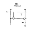
- FIG. 1 is an equivalent circuit diagram showing a pixel of a conventional active matrix organic light-emitting display.
- the pixel circuit may include an organic LED OLED, a switching transistor SM, a driving transistor DM, and a capacitor Cst.
- the two transistors SM and DM may be PMOS transistors.
- a current I OLED corresponding to a voltage V GS charged between the gate and source ofthe driving transistor DM according to the capacitor Cst, may flow through the driving transistor DM, thereby causing the organic LED OLED to emit light.
- a current corresponding to the data voltage may be supplied to the organic LED, thereby causing it to emit light with at a luminance corresponding to the current.
- the data voltage may have multiple values in a specific range in order to represent a predetermined gray scale.
- the organic light-emitting display may not display correct images because the driving transistors of the pixels may have different threshold voltages.
- the present invention provides a light-emitting display having a pixel circuit that may compensate for the threshold voltage of a driving transistor.
- the present invention provides a light-emitting display that may reduce the influence of kickback caused by parasitic capacitance existing in the pixel circuit.
- the present invention discloses a light-emitting display comprising a plurality of data lines transmitting a data voltage, a plurality of scan lines transmitting a select signal, and a plurality of pixel circuits coupled to the scan lines and the data lines.
- a pixel circuit includes first, second, third, and fourth transistors, a first capacitor, and a light-emitting element.
- the first and second transistors are serially coupled to each other and turned on in response to a first control signal.
- the first capacitor is coupled in parallel with the first and second transistors.
- the third transistor supplies the data voltage to a first electrode of the first capacitor in response to the select signal.
- the fourth transistor outputs a current corresponding to its gate-source voltage, which is based on a voltage of the first capacitor.
- the light-emitting element emits light in response to the current from the fourth transistor.
- the present invention also discloses a light-emitting display comprising a plurality of data lines transmitting a data voltage, a plurality of scan lines transmitting select signals including first and second select signals, and a plurality of pixel circuits coupled to the scan lines and the data lines.
- a pixel circuit includes first through sixth transistors, first and second capacitors, and a light-emitting element.
- the first transistor includes a first electrode coupled to a data line and a second electrode turned on in response to the second select signal to transmit the data voltage, and the first capacitor is charged with a voltage corresponding to the data voltage.
- the second and third transistors are serially coupled to each other, coupled in parallel with the first capacitor, and turned on in response to the first select signal.
- the fourth transistor outputs a current corresponding to the voltage charged in the first capacitor.
- the fifth and sixth transistors are serially coupled to each other and turned on in response to the first select signal to diode-connect the fourth transistor.
- the second capacitor is coupled between a first electrode of the first capacitor and a control electrode of the fourth transistor, and it is charged with a voltage corresponding to the threshold voltage of the fourth transistor.
- the light-emitting element emits light corresponding to the current output from the fourth transistor.
- the present invention discloses a light-emitting display comprising a plurality of data lines transmitting a data voltage, a plurality of scan lines transmitting select signals including first and second select signals, and a plurality of pixel circuits coupled to the scan lines and the data lines.
- a pixel circuit includes first, third, fourth and fifth transistors, a first capacitor, and a light-emitting element.
- the first transistor includes a first electrode coupled to a data line, and a second electrode is turned on in response to the second select signal to transmit the data voltage.
- the first capacitor is charged with a voltage corresponding to the data voltage.
- the third transistor outputs a current corresponding to the voltage charged in the first capacitor.
- the fourth and fifth transistors are serially coupled to each other and turned on in response to the first select signal to diode-connect the third transistor.
- the light-emitting element emits light corresponding to the current output from the third transistor.
- FIG. 1 is an equivalent circuit diagram showing a pixel of a conventional active matrix organic light-emitting display.
- FIG. 2 shows a configuration of an organic light-emitting display according to a first exemplary embodiment not falling within the scope of the appended claims..
- FIG. 3 is an equivalent circuit diagram showing a pixel circuit of the organic light-emitting display of FIG. 2.
- FIG. 4 shows waveforms that may be applied to pixel circuits of exemplary embodiments of the present invention.
- FIG. 5 is an equivalent circuit diagram showing a pixel circuit according to a second exemplary embodiment of the present invention.
- FIG. 6 is an equivalent circuit diagram showing a pixel circuit according to a third exemplary embodiment of the present invention.
- FIG. 7 is an equivalent circuit diagram showing a pixel circuit according to a fourth exemplary embodiment ofthe present invention.
- FIG. 2 shows the configuration of an organic light-emitting display according to a first exemplary embodiment of the present invention.
- the organic light-emitting display may include an organic light-emitting display panel 100, a scan driver 200, a data driver 300, and a light emission control signal driver 400.
- the organic light-emitting display panel 100 may include a plurality of data lines D 1 to D m arranged in a column direction, a plurality of scan lines S 1 to S n arranged in a row direction, a plurality of light emission control lines E 1 to E n , and a plurality of pixel circuits 110.
- the data lines D 1 to D m may transmit data signals corresponding to video signals to the pixel circuits 110
- the scan lines S 1 to S n may transmit select signals to the pixel circuits 110.
- the scan driver 200 may sequentially generate the select signals and supply them to the scan lines S 1 to S n .
- a scan line transmitting the current select signal may be called a "current scan line,” and a scan line transmitting the select signal before the current select signal is transmitted may be called a "previous scan line”.
- the data driver 300 may generate a data voltage corresponding to a video signal and supply the data voltage to the data lines D 1 to D m .
- the light emission control signal driver 400 may sequentially apply a light emission control signal, for controlling light emission of organic light-emitting elements, to the light emission control lines E 1 to E n .
- Various methods may be used to couple the scan driver 200, the data driver 300, and/or the light emission control signal driver 400 to the display panel 100.
- they may be mounted in the form of chip on a tape carrier package coupled to the display panel, they may be mounted in the form of chip on a flexible printed circuit or a film attached to and coupled to the display panel, and they may be directly mounted on the panel's glass substrate.
- they may be replaced by a driving circuit formed of the same layers as the scan lines, data lines, and thin film transistors on the glass substrate.
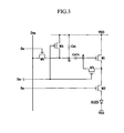
- FIG. 3 is an equivalent circuit diagram showing a pixel circuit 110 according to a first exemplary embodiment not falling within the scope of the appended claims.
- the pixel circuit may include five transistors M1, M2, M3, M4 and M5, two capacitors Cst and Cvth, and an organic LED OLED.
- the five transistors M1 to M5 may be PMOS transistors.
- the transistor M1 drives the organic LED OLED, and it may be coupled between a power supply for providing a power supply voltage V DD and the organic LED OLED.
- the transistor M1 controls the current that flows through the organic LED OLED, via the transistor M2, in response to a voltage applied to the gate of the transistor M1.
- the transistor M3 may diode-connect the transistor M1 in response to a select signal from the previous scan line Sn-1.
- the gate of the transistor M1 may be coupled to node A of the capacitor Cvth.
- the capacitor Cst and the transistor M4 may be coupled in parallel to each other and between node B of the capacitor Cvth and the power supply providing the voltage V DD .
- the transistor M4 may provide the voltage V DD to node B of the capacitor Cvth in response to the select signal from the previous scan line Sn-1.
- the transistor M4 may be coupled to a power supply voltage that differs from the power supply voltage V DD .
- the transistor M5 may deliver a data signal transmitted from the data line Dm to node B of the capacitor Cvth in response to the select signal from the current scan line Sn.
- the transistor M2 may be coupled between the drain of the transistor M1 and the anode of the organic LED OLED, and it may block the drain of the transistor M 1 from the organic LED OLED in response to the select signal from the light emission control line En.
- the organic LED OLED emits light in response to a current input thereto from the transistor M1 via the transistor M2.
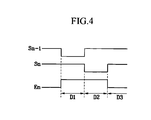
- FIG. 4 shows waveforms that may be applied to the pixel circuit 110.
- V CvthA and V CvthB are the voltages applied to nodes A and B ofthe capacitor Cvth, respectively.
- a high level signal may be applied to the light emission control line En, thus turning off the transistor M2. This prevents the current flowing through the transistor M1 from flowing to the organic LED OLED. Furthermore, a high level signal may be applied to the current scan line Sn to turn off the transistor M5.
- Equation 3 represents the gate-source voltage Vgs of the transistor M1.
- the light emission control line En may be provided with a high level signal, which keeps the transistor M2 turned off.
- the transistor M2 may be turned on in response to a low-level light emission control signal of the light emission control line En, thereby providing the current I OLED , corresponding to the gate-source voltage Vgs of the transistor M1, to the organic LED OLED to emit light.
- Equation 4 represents the current I OLED .
- I OLED is the current flowing in the organic LED OLED
- Vgs is the gate-source voltage of the transistor M1
- Vth is the threshold voltage of the transistor M1.
- Vdata is the data voltage
- ⁇ is a constant. Equation 4 shows that the display panel may be stably driven because the current I OLED is determined by the data voltage Vdata and the power supply voltage V DD , irrespective of the threshold voltage Vth of the driving transistor M1.
- the signal waveforms shown in FIG. 4 are exemplary, and they may be modified.
- the starting point of the high level signal applied to the light emission control line En may lag behind the starting point of the low level select signal applied to the previous scan line Sn-1.
- the end point ofthe high level signal applied to the light emission control line En may lag behind the end point ofthe low level select signal applied to the current scan line Sn.
- applying the low level select signal to the previous scan line Sn-1 turns off the transistors M3 and M4, and applying the low level select signal to the current scan line Sn turns on the transistor M5, thereby providing node B ofthe capacitor Cst with the data voltage. Accordingly, the voltage corresponding to the data voltage may be charged in the capacitor Cst while the driving transistor M1 is turned on. According to the voltage charged in the capacitor Cst, the gate-source voltage Vgs of the driving transistor M1 maybe continuously maintained, even when the switching transistor M5 is turned off and the data voltage is not supplied to node B.
- parasitic capacitance existing in node B may generate a voltage variation ⁇ V in the voltage supplied to node B, which may result in a voltage shift in node B.
- This voltage shift is called kickback, and the voltage variation ⁇ V is called kickback voltage.
- the kickback may generate a sticking image when displaying images and degrade the display panel's display characteristics.
- the kickback voltage is greater than a gray-scale level interval, the display quality of the display panel may significantly deteriorate, such that images with the same gray scales may be displayed differently.
- FIG. 5 is an equivalent circuit diagram showing a pixel circuit according to a second exemplary embodiment of the present invention. This pixel circuit differs from the pixel circuit of the first exemplary embodiment in that dual transistors M4_1 and M4_2 are employed to reduce the kickback voltage at node B.
- the pixel circuit may include six transistors M1, M2, M3, M4_1, M4_2, and M5, two capacitors Cst and Cvth, and an organic LED OLED.
- the four transistors M1, M2, M3, and M5, the two capacitors Cst and Cvth, and the organic LED OLED may be identically configured and operated as in the first exemplary embodiment. Hence, detailed explanations thereof are omitted.
- the source ofthe transistor M4_2 may be coupled to the power supply voltage V DD , and its drain may be coupled to the source of the transistor M4_1.
- the drain of the transistor M4_1 may be coupled to the drain of the transistor M5. That is, the two transistors M4_1 and M4_2 may form dual transistors that are serially coupled to each other.
- the gates of the transistors M4_1 and M4_2 may be coupled to the previous scan line Sn-1. Accordingly, the two transistors M4_1 and M4_2 may be simultaneously turned on in response to a previous select signal to supply the power supply voltage V DD to an end ofthe capacitor Cst.
- Turning the transistors M4_1 and M4_2 off and turning the transistor M5 may reduce the kickback voltage at node B. Accordingly, a variation in the data voltage applied to node B and a voltage variation in the gate node A of the transistor M1 may decrease. Consequently, a variation in the gate-source voltage Vgs of the transistor M1, caused by the kickback voltage, may decrease, thereby reducing the influence of kickback on the current transmitted to the organic LED OLED.
- the kickback voltage may be more effectively reduced when the channel of the transistor M4_2 is longer than the channel of the transistor M4_1.
- Table 1 shows voltages of node B with the dual transistors M4_1 and M4_2 turned on and turned off, in the case where they each have a channel width W of 5 ⁇ m, and the channel length L of the transistor M4_1 plus the channel length L of transistor M4_2 is 20 ⁇ m.
- Table 1 shows that as the channel length L ofthe transistor M4_2 increases, the kickback voltage at node B decreases. That is, when the channel of the transistor M4_2 is longer than the channel of the transistor M4_1, the current I OLED corresponding to the data voltage may be more stably supplied to the organic LED OLED, thereby improving the display panel's display characteristics.
- Table 1 shows the minimum channel length ofthe transistor M4_1 as 5 ⁇ m, it may be less than 5 ⁇ m if the transistor's characteristics are secured when it is fabricated with a channel length shorter than 5 ⁇ m. As the channel length L of the transistor M4_1 shortens, parasitic capacitance decreases, and the influence of kickback may decrease.
- the pixel circuit shown in FIG. 5 employs the serially coupled dual transistors M4_1 and M4_2, the pixel circuit may alternatively use a dual-gate transistor. While the dual transistors indicate that two transistors formed one source region, one drain region and one gate electrode are coupled to each other, the dual gate transistor indicates that one transistor has one source region, one drain region and two gate electrodes connected each other.
- FIG. 6 is an equivalent circuit diagram showing a pixel circuit according to the third exemplary embodiment of the present invention.
- the pixel circuit differs from the pixel circuit of the first exemplary embodiment in that dual transistors M3_1 and M3_2 are employed to reduce the kickback voltage caused by parasitic capacitance existing between the gate and source of the transistor M1.
- the pixel circuit may include six transistors M1, M2, M3_1, M3_2, M4, and M5, two capacitors Cst and Cvth, and an organic LED OLED.
- the four transistors M1, M2, M4, and M5, the two capacitors Cst and Cvth, and the organic LED OLED may be identically configured and operated as in the first exemplary embodiment. Hence, detailed explanations thereof are omitted.
- the source of the transistor M3_2 may be coupled to the drain of the transistor M1, and its drain may be coupled to the source of the transistor M3_1.
- the drain of the transistor M3_1 may be coupled to the gate of the transistor M1. That is, the two transistors M3_1 and M3_2 form dual transistors that are serially coupled to each other.
- the gates ofthe transistors M3_1 and M3_2 may be coupled to the previous scan line Sn-1. Accordingly, the two transistors M3_1 and M3_2 may be simultaneously turned on in response to the previous select signal to diode-connect the transistor M1.
- Turning off the transistors M3_1 and M3_2 and turning on the transistor M5 may reduce the kickback voltage at node A. Accordingly, the influence of voltage variation due to the kickback voltage at gate node A ofthe transistor M1 may be decreased, thereby decreasing a variation in the gate-source voltage Vgs of the transistor M1 caused by the kickback voltage. Consequently, the influence of kickback on the current I OLED transmitted to the organic LED OLED may be reduced.
- the kickback voltage may be more effectively reduced when the channel of the transistor M3_2 is longer than the channel of the transistor M3_1.
- Table 2 shows voltages of node A (i.e. the gate of the transistor M1), with the dual transistors M3_1 and M3_2 turned on and turned off, in the case where they each have a channel width W of 5 ⁇ m, and the channel length L of the transistor M3_1 plus the channel length L of the transistor M3_2 is 20 ⁇ m.
- Table 2 shows that as the channel length L ofthe transistor M3_2 increases, the kickback voltage at the gate of the transistor M1 decreases. That is, when the channel of the transistor M3_2 is longer than the channel of the transistor M3_1, the current I OLED corresponding to the data voltage may be more stably supplied to the organic LED OLED, thereby improving the display panel's display characteristics.
- FIG. 6 shows the pixel circuit with the serially coupled dual transistors M3_1 and M3_2, the pixel circuit may alternative use a dual-gate transistor.
- Table 2 shows the minimum channel length of the transistor M3_1 as 5 ⁇ m, it maybe reduced to less than 5 ⁇ m if the transistor's characteristics are secured even when it is fabricated with a channel length shorter than 5 ⁇ m. As the channel length of the transistor M3_1 shortens, parasitic capacitance may decrease, and the influence of kickback may decrease.
- FIG. 7 is an equivalent circuit diagram showing a pixel circuit according to the fourth exemplary embodiment of the present invention.
- the pixel circuit differs from the pixel circuits of the second and third exemplary embodiments in that dual transistors M4_1 and M4_2 may be employed to reduce the kickback voltage at node B, and dual transistors M3_1 and M3_2 may be used to reduce the kickback voltage caused by parasitic capacitance existing between the gate and source of the transistor M1.
- the pixel circuit may include seven transistors M1, M2, M3_1, M3_2, M4_1, M4_2, and M5, two capacitors Cst and Cvth, and an organic LED OLED.
- the three transistors M1, M2, and M5, the two capacitors Cst and Cvth, and the organic LED OLED may be identically configured and operated as in the first exemplary embodiment, of FIG. 3, the transistors M4_1 and M4_2 may be identical to those of the pixel circuit of the second exemplary embodiment, of FIG. 5, and the configuration and operation of the transistors M3_1 and M3_2 may be identical to those of the pixel circuit of the third exemplary embodiment of FIG. 6. Thus, detailed explanations thereof are omitted.
- using the transistors M3_1, M3_2 and the transistors M4_1, M4_2 may simultaneously reduce the kickback voltage at node B and the kickback voltage caused by the parasitic capacitance between the gate and source of the transistor M1.
- exemplary embodiments ofthe present invention use dual transistors to reduce the kickback voltage caused by a parasitic capacitance component existing in the pixel circuit.
- dual transistors having different channel lengths may be coupled in parallel with the capacitor charged with a voltage corresponding to a data voltage to reduce the influence of kickback on an electrode of the capacitor.
- the kickback voltage caused by parasitic capacitance existing between the gate and source/drain of the transistor driving the organic LED may be reduced using dual transistors having different sizes. This may effectively decrease the influence of kickback on the gate of the driving transistor. Consequently, the influence of kickback may be reduced, thereby improving the display characteristics ofthe light-emitting display.
Landscapes
- Engineering & Computer Science (AREA)
- Physics & Mathematics (AREA)
- Computer Hardware Design (AREA)
- General Physics & Mathematics (AREA)
- Theoretical Computer Science (AREA)
- Control Of Indicators Other Than Cathode Ray Tubes (AREA)
- Control Of El Displays (AREA)
- Electroluminescent Light Sources (AREA)
- Devices For Indicating Variable Information By Combining Individual Elements (AREA)
- Led Device Packages (AREA)
Abstract
Description
- The present invention relates to a light-emitting display, and more specifically, to an organic light-emitting display using luminescence of an organic material.
- Generally, an organic light-emitting display emits light with an organic light-emitting element that uses luminescence of an organic material. NxM organic light-emitting cells, arranged in a matrix form, may be driven with a voltage or current to display images. The organic light-emitting cell may also be called an organic LED (light-emitting diode) because it has diode characteristics, and it may include an anode (ITO), an organic thin film, and a cathode (metal). The organic thin film may have a multi-layer structure including an emitting layer (EML), an electron transport layer (ETL), and a hole transport layer (HTL) for balancing electrons and holes to improve luminescence efficiency. The organic thin film may further include an electron injecting layer (EIL) and a hole injecting layer (HIL).
- Organic light-emitting cells may be driven by a passive matrix driving method or an active matrix driving method, which may use a thin film transistor (TFT) or a MOSFET. The passive matrix organic EL display may be constructed having an anode and a cathode that are perpendicular to each other, and a line may be selected to drive the light-emitting cells. The active matrix display may comprise a TFT coupled to each ITO pixel electrode, and it may be driven by a voltage maintained by a capacitor coupled to the gate ofthe TFT.
- A conventional active matrix organic light-emitting display will now be explained.
- FIG. 1 is an equivalent circuit diagram showing a pixel of a conventional active matrix organic light-emitting display. Referring to FIG. 1, the pixel circuit may include an organic LED OLED, a switching transistor SM, a driving transistor DM, and a capacitor Cst. The two transistors SM and DM may be PMOS transistors.
- When the switching transistor SM turns on in response to a select signal applied to its gate from a signal line Sn, a data voltage VDATA from a data line Dm is supplied to the gate of the driving transistor DM. Then, a current IOLED, corresponding to a voltage VGS charged between the gate and source ofthe driving transistor DM according to the capacitor Cst, may flow through the driving transistor DM, thereby causing the organic LED OLED to emit light. Here, the current IOLED may be represented by
Equation 1.
- In the pixel circuit of FIG. 1, a current corresponding to the data voltage may be supplied to the organic LED, thereby causing it to emit light with at a luminance corresponding to the current. The data voltage may have multiple values in a specific range in order to represent a predetermined gray scale.
- As
Equation 1 shows, however, the current IOLED varies with the threshold voltage VTH of the driving transistor DM. Accordingly, the organic light-emitting display may not display correct images because the driving transistors of the pixels may have different threshold voltages. - The present invention provides a light-emitting display having a pixel circuit that may compensate for the threshold voltage of a driving transistor.
- The present invention provides a light-emitting display that may reduce the influence of kickback caused by parasitic capacitance existing in the pixel circuit.
- Additional features of the invention will be set forth in the description which follows, and in part will be apparent from the description, or may be learned by practice ofthe invention.
- The present invention discloses a light-emitting display comprising a plurality of data lines transmitting a data voltage, a plurality of scan lines transmitting a select signal, and a plurality of pixel circuits coupled to the scan lines and the data lines. A pixel circuit includes first, second, third, and fourth transistors, a first capacitor, and a light-emitting element. The first and second transistors are serially coupled to each other and turned on in response to a first control signal. The first capacitor is coupled in parallel with the first and second transistors. The third transistor supplies the data voltage to a first electrode of the first capacitor in response to the select signal. The fourth transistor outputs a current corresponding to its gate-source voltage, which is based on a voltage of the first capacitor. The light-emitting element emits light in response to the current from the fourth transistor.
- The present invention also discloses a light-emitting display comprising a plurality of data lines transmitting a data voltage, a plurality of scan lines transmitting select signals including first and second select signals, and a plurality of pixel circuits coupled to the scan lines and the data lines. A pixel circuit includes first through sixth transistors, first and second capacitors, and a light-emitting element. The first transistor includes a first electrode coupled to a data line and a second electrode turned on in response to the second select signal to transmit the data voltage, and the first capacitor is charged with a voltage corresponding to the data voltage. The second and third transistors are serially coupled to each other, coupled in parallel with the first capacitor, and turned on in response to the first select signal. The fourth transistor outputs a current corresponding to the voltage charged in the first capacitor. The fifth and sixth transistors are serially coupled to each other and turned on in response to the first select signal to diode-connect the fourth transistor. The second capacitor is coupled between a first electrode of the first capacitor and a control electrode of the fourth transistor, and it is charged with a voltage corresponding to the threshold voltage of the fourth transistor. The light-emitting element emits light corresponding to the current output from the fourth transistor.
- The present invention discloses a light-emitting display comprising a plurality of data lines transmitting a data voltage, a plurality of scan lines transmitting select signals including first and second select signals, and a plurality of pixel circuits coupled to the scan lines and the data lines. A pixel circuit includes first, third, fourth and fifth transistors, a first capacitor, and a light-emitting element. The first transistor includes a first electrode coupled to a data line, and a second electrode is turned on in response to the second select signal to transmit the data voltage. The first capacitor is charged with a voltage corresponding to the data voltage. The third transistor outputs a current corresponding to the voltage charged in the first capacitor. The fourth and fifth transistors are serially coupled to each other and turned on in response to the first select signal to diode-connect the third transistor. The light-emitting element emits light corresponding to the current output from the third transistor.
- It is to be understood that both the foregoing general description and the following detailed description are exemplary and explanatory and are intended to provide further explanation of the invention as claimed.
- The accompanying drawings, which are included to provide a further understanding of the invention and are incorporated in and constitute a part of this specification, illustrate embodiments of the invention and together with the description serve to explain the principles ofthe invention.
- FIG. 1 is an equivalent circuit diagram showing a pixel of a conventional active matrix organic light-emitting display.
- FIG. 2 shows a configuration of an organic light-emitting display according to a first exemplary embodiment not falling within the scope of the appended claims..
- FIG. 3 is an equivalent circuit diagram showing a pixel circuit of the organic light-emitting display of FIG. 2.
- FIG. 4 shows waveforms that may be applied to pixel circuits of exemplary embodiments of the present invention.
- FIG. 5 is an equivalent circuit diagram showing a pixel circuit according to a second exemplary embodiment of the present invention.
- FIG. 6 is an equivalent circuit diagram showing a pixel circuit according to a third exemplary embodiment of the present invention.
- FIG. 7 is an equivalent circuit diagram showing a pixel circuit according to a fourth exemplary embodiment ofthe present invention.
- The following detailed description shows and describes exemplary embodiments of the present invention, simply by way of illustration of the best mode contemplated by the inventors of carrying out the invention. As will be realized, the invention is capable of modification in various obvious respects, all without departing from the invention. Accordingly, the drawings and description are to be regarded as illustrative in nature, and not restrictive. To clarify the present invention, parts which are not described in the specification are omitted, and parts for which similar descriptions are provided have the same reference numerals.
- FIG. 2 shows the configuration of an organic light-emitting display according to a first exemplary embodiment of the present invention.
- Referring to FIG. 2, the organic light-emitting display may include an organic light-emitting
display panel 100, ascan driver 200, adata driver 300, and a light emissioncontrol signal driver 400. - The organic light-emitting
display panel 100 may include a plurality of data lines D1 to Dm arranged in a column direction, a plurality of scan lines S1 to Sn arranged in a row direction, a plurality of light emission control lines E1 to En, and a plurality ofpixel circuits 110. The data lines D1 to Dm may transmit data signals corresponding to video signals to thepixel circuits 110, and the scan lines S1 to Sn may transmit select signals to thepixel circuits 110. - The
scan driver 200 may sequentially generate the select signals and supply them to the scan lines S1 to Sn. A scan line transmitting the current select signal may be called a "current scan line," and a scan line transmitting the select signal before the current select signal is transmitted may be called a "previous scan line". - The
data driver 300 may generate a data voltage corresponding to a video signal and supply the data voltage to the data lines D1 to Dm. The light emissioncontrol signal driver 400 may sequentially apply a light emission control signal, for controlling light emission of organic light-emitting elements, to the light emission control lines E1 to En. - Various methods may be used to couple the
scan driver 200, thedata driver 300, and/or the light emissioncontrol signal driver 400 to thedisplay panel 100. For example, they may be mounted in the form of chip on a tape carrier package coupled to the display panel, they may be mounted in the form of chip on a flexible printed circuit or a film attached to and coupled to the display panel, and they may be directly mounted on the panel's glass substrate. Alternatively, they may be replaced by a driving circuit formed of the same layers as the scan lines, data lines, and thin film transistors on the glass substrate. - FIG. 3 is an equivalent circuit diagram showing a
pixel circuit 110 according to a first exemplary embodiment not falling within the scope of the appended claims. Referring to FIG. 3, the pixel circuit may include five transistors M1, M2, M3, M4 and M5, two capacitors Cst and Cvth, and an organic LED OLED. The five transistors M1 to M5 may be PMOS transistors. - The transistor M1 drives the organic LED OLED, and it may be coupled between a power supply for providing a power supply voltage VDD and the organic LED OLED. The transistor M1 controls the current that flows through the organic LED OLED, via the transistor M2, in response to a voltage applied to the gate of the transistor M1. The transistor M3 may diode-connect the transistor M1 in response to a select signal from the previous scan line Sn-1.
- The gate of the transistor M1 may be coupled to node A of the capacitor Cvth. The capacitor Cst and the transistor M4 may be coupled in parallel to each other and between node B of the capacitor Cvth and the power supply providing the voltage VDD. The transistor M4 may provide the voltage VDD to node B of the capacitor Cvth in response to the select signal from the previous scan line Sn-1. Alternatively, the transistor M4 may be coupled to a power supply voltage that differs from the power supply voltage VDD.
- The transistor M5 may deliver a data signal transmitted from the data line Dm to node B of the capacitor Cvth in response to the select signal from the current scan line Sn. The transistor M2 may be coupled between the drain of the transistor M1 and the anode of the organic LED OLED, and it may block the drain of the
transistor M 1 from the organic LED OLED in response to the select signal from the light emission control line En. The organic LED OLED emits light in response to a current input thereto from the transistor M1 via the transistor M2. - The operation of the
pixel circuit 110 will now be explained with reference to FIG. 4, which shows waveforms that may be applied to thepixel circuit 110. - Applying a low level scan voltage to the previous scan line Sn-1, during a period D1, turns on the transistor M3 and diode-connects the transistor M1. Accordingly, the gate-source voltage of the transistor M1 may reach the threshold voltage Vth of the transistor M1. Here, the voltage that may be applied to the gate of the transistor M1, that is, node A of the capacitor Cvth, corresponds to the sum ofthe power supply voltage VDD and the threshold voltage Vth ofthe transistor M1 because its source is coupled to the power supply voltage VDD. Furthermore, applying the low level scan voltage to the previous scan line Sn-1 turns on the transistor M4, thereby supplying the power supply voltage VDD to node B of the capacitor Cvth. Equation 2 represents the voltage VCvth that may be charged in the capacitor Cvth.

- Here, VCvthA and VCvthB are the voltages applied to nodes A and B ofthe capacitor Cvth, respectively.
- During the period D1, a high level signal may be applied to the light emission control line En, thus turning off the transistor M2. This prevents the current flowing through the transistor M1 from flowing to the organic LED OLED. Furthermore, a high level signal may be applied to the current scan line Sn to turn off the transistor M5.
- Applying a low level scan voltage to the current scan line Sn, during the following period D2, turns on the transistor M5, thereby supplying a data voltage Vdata to node B of the capacitor Cvth. Additionally, the gate of the
transistor M 1 may be provided with a voltage corresponding to the sum of the data voltage Vdata and its threshold voltage Vth because the capacitor Cvth is charged with a voltage corresponding to the threshold voltage Vth ofthe transistor M1. That is, Equation 3 represents the gate-source voltage Vgs of the transistor M1. Here, the light emission control line En may be provided with a high level signal, which keeps the transistor M2 turned off.
- During a period D3, the transistor M2 may be turned on in response to a low-level light emission control signal of the light emission control line En, thereby providing the current IOLED, corresponding to the gate-source voltage Vgs of the transistor M1, to the organic LED OLED to emit light. Equation 4 represents the current IOLED.

- Here, IOLED is the current flowing in the organic LED OLED, Vgs is the gate-source voltage of the transistor M1, and Vth is the threshold voltage of the transistor M1. Additionally, Vdata is the data voltage and β is a constant. Equation 4 shows that the display panel may be stably driven because the current IOLED is determined by the data voltage Vdata and the power supply voltage VDD, irrespective of the threshold voltage Vth of the driving transistor M1.
- The signal waveforms shown in FIG. 4 are exemplary, and they may be modified. For example, the starting point of the high level signal applied to the light emission control line En may lag behind the starting point of the low level select signal applied to the previous scan line Sn-1. Furthermore, the end point ofthe high level signal applied to the light emission control line En may lag behind the end point ofthe low level select signal applied to the current scan line Sn.
- As described above, applying the low level select signal to the previous scan line Sn-1 turns off the transistors M3 and M4, and applying the low level select signal to the current scan line Sn turns on the transistor M5, thereby providing node B ofthe capacitor Cst with the data voltage. Accordingly, the voltage corresponding to the data voltage may be charged in the capacitor Cst while the driving transistor M1 is turned on. According to the voltage charged in the capacitor Cst, the gate-source voltage Vgs of the driving transistor M1 maybe continuously maintained, even when the switching transistor M5 is turned off and the data voltage is not supplied to node B.
- However, parasitic capacitance existing in node B may generate a voltage variation ΔV in the voltage supplied to node B, which may result in a voltage shift in node B. This voltage shift is called kickback, and the voltage variation ΔV is called kickback voltage. The kickback may generate a sticking image when displaying images and degrade the display panel's display characteristics. When the kickback voltage is greater than a gray-scale level interval, the display quality of the display panel may significantly deteriorate, such that images with the same gray scales may be displayed differently.
- Exemplary embodiments of the present invention for solving the effect of the kickback will now be explained in detail.
- FIG. 5 is an equivalent circuit diagram showing a pixel circuit according to a second exemplary embodiment of the present invention. This pixel circuit differs from the pixel circuit of the first exemplary embodiment in that dual transistors M4_1 and M4_2 are employed to reduce the kickback voltage at node B.
- Referring to FIG. 5, the pixel circuit may include six transistors M1, M2, M3, M4_1, M4_2, and M5, two capacitors Cst and Cvth, and an organic LED OLED. The four transistors M1, M2, M3, and M5, the two capacitors Cst and Cvth, and the organic LED OLED may be identically configured and operated as in the first exemplary embodiment. Hence, detailed explanations thereof are omitted.
- The source ofthe transistor M4_2 may be coupled to the power supply voltage VDD, and its drain may be coupled to the source of the transistor M4_1. The drain of the transistor M4_1 may be coupled to the drain of the transistor M5. That is, the two transistors M4_1 and M4_2 may form dual transistors that are serially coupled to each other. The gates of the transistors M4_1 and M4_2 may be coupled to the previous scan line Sn-1. Accordingly, the two transistors M4_1 and M4_2 may be simultaneously turned on in response to a previous select signal to supply the power supply voltage VDD to an end ofthe capacitor Cst.
- Turning the transistors M4_1 and M4_2 off and turning the transistor M5 may reduce the kickback voltage at node B. Accordingly, a variation in the data voltage applied to node B and a voltage variation in the gate node A of the transistor M1 may decrease. Consequently, a variation in the gate-source voltage Vgs of the transistor M1, caused by the kickback voltage, may decrease, thereby reducing the influence of kickback on the current transmitted to the organic LED OLED.
- When the total channel length of the dual transistors M4_1 and M4_2 is kept constant, the kickback voltage may be more effectively reduced when the channel of the transistor M4_2 is longer than the channel of the transistor M4_1.
- Table 1 shows voltages of node B with the dual transistors M4_1 and M4_2 turned on and turned off, in the case where they each have a channel width W of 5 µm, and the channel length L of the transistor M4_1 plus the channel length L of transistor M4_2 is 20µm.
[Table 1] Transistor size Node B voltage Kickback voltage M4_1(W/L) M4_2(W/L) When turned on When turned off 5/15µm 5/5µm 5.0V 5.4917V 0.4917V 5/10µm 5/10µm 5.0V 5.3811V 0.3811V 5/7µm 5/13µm 5.0V 5.3217V 0.3217V 5/5µm 5/15µm 5.0V 5.2834V 0.2834V - Table 1 shows that as the channel length L ofthe transistor M4_2 increases, the kickback voltage at node B decreases. That is, when the channel of the transistor M4_2 is longer than the channel of the transistor M4_1, the current IOLED corresponding to the data voltage may be more stably supplied to the organic LED OLED, thereby improving the display panel's display characteristics.
- While Table 1 shows the minimum channel length ofthe transistor M4_1 as 5µm, it may be less than 5µm if the transistor's characteristics are secured when it is fabricated with a channel length shorter than 5µm. As the channel length L of the transistor M4_1 shortens, parasitic capacitance decreases, and the influence of kickback may decrease.
- While the pixel circuit shown in FIG. 5 employs the serially coupled dual transistors M4_1 and M4_2, the pixel circuit may alternatively use a dual-gate transistor. While the dual transistors indicate that two transistors formed one source region, one drain region and one gate electrode are coupled to each other, the dual gate transistor indicates that one transistor has one source region, one drain region and two gate electrodes connected each other.
- A third exemplary embodiment of the present invention will now be explained.
- FIG. 6 is an equivalent circuit diagram showing a pixel circuit according to the third exemplary embodiment of the present invention. The pixel circuit differs from the pixel circuit of the first exemplary embodiment in that dual transistors M3_1 and M3_2 are employed to reduce the kickback voltage caused by parasitic capacitance existing between the gate and source of the transistor M1.
- Referring to FIG. 6, the pixel circuit may include six transistors M1, M2, M3_1, M3_2, M4, and M5, two capacitors Cst and Cvth, and an organic LED OLED. The four transistors M1, M2, M4, and M5, the two capacitors Cst and Cvth, and the organic LED OLED may be identically configured and operated as in the first exemplary embodiment. Hence, detailed explanations thereof are omitted.
- The source of the transistor M3_2 may be coupled to the drain of the transistor M1, and its drain may be coupled to the source of the transistor M3_1. The drain of the transistor M3_1 may be coupled to the gate of the transistor M1. That is, the two transistors M3_1 and M3_2 form dual transistors that are serially coupled to each other. The gates ofthe transistors M3_1 and M3_2 may be coupled to the previous scan line Sn-1. Accordingly, the two transistors M3_1 and M3_2 may be simultaneously turned on in response to the previous select signal to diode-connect the transistor M1.
- Turning off the transistors M3_1 and M3_2 and turning on the transistor M5 may reduce the kickback voltage at node A. Accordingly, the influence of voltage variation due to the kickback voltage at gate node A ofthe transistor M1 may be decreased, thereby decreasing a variation in the gate-source voltage Vgs of the transistor M1 caused by the kickback voltage. Consequently, the influence of kickback on the current IOLED transmitted to the organic LED OLED may be reduced.
- When the total channel length of the dual transistors M3_1 and M3_2 is kept constant, the kickback voltage may be more effectively reduced when the channel of the transistor M3_2 is longer than the channel of the transistor M3_1.
- Table 2 shows voltages of node A (i.e. the gate of the transistor M1), with the dual transistors M3_1 and M3_2 turned on and turned off, in the case where they each have a channel width W of 5µm, and the channel length L of the transistor M3_1 plus the channel length L of the transistor M3_2 is 20µm.
[Table 2] Transistor size Gate voltage of transistor M1 Kickback voltage M3_1(W/L) M3_2(W/L) When turned on When turned off 5/15µm 5/5µm 3.6570V 4.6653V 1.0083V 5/10µm 5/10µm 3.2503V 4.1223V 0.8720V 5/7µm 5/13µm 3.1370V 3.9445V 0.8075V 5/5µm 5/15µm 3.0791V 3.8463V 0.7672V - Table 2 shows that as the channel length L ofthe transistor M3_2 increases, the kickback voltage at the gate of the transistor M1 decreases. That is, when the channel of the transistor M3_2 is longer than the channel of the transistor M3_1, the current IOLED corresponding to the data voltage may be more stably supplied to the organic LED OLED, thereby improving the display panel's display characteristics.
- While FIG. 6 shows the pixel circuit with the serially coupled dual transistors M3_1 and M3_2, the pixel circuit may alternative use a dual-gate transistor. While Table 2 shows the minimum channel length of the transistor M3_1 as 5µm, it maybe reduced to less than 5µm if the transistor's characteristics are secured even when it is fabricated with a channel length shorter than 5µm. As the channel length of the transistor M3_1 shortens, parasitic capacitance may decrease, and the influence of kickback may decrease.
- A fourth exemplary embodiment of the present invention will now be explained.
- FIG. 7 is an equivalent circuit diagram showing a pixel circuit according to the fourth exemplary embodiment of the present invention. The pixel circuit differs from the pixel circuits of the second and third exemplary embodiments in that dual transistors M4_1 and M4_2 may be employed to reduce the kickback voltage at node B, and dual transistors M3_1 and M3_2 may be used to reduce the kickback voltage caused by parasitic capacitance existing between the gate and source of the transistor M1.
- Referring to FIG. 7, the pixel circuit may include seven transistors M1, M2, M3_1, M3_2, M4_1, M4_2, and M5, two capacitors Cst and Cvth, and an organic LED OLED. The three transistors M1, M2, and M5, the two capacitors Cst and Cvth, and the organic LED OLED may be identically configured and operated as in the first exemplary embodiment, of FIG. 3, the transistors M4_1 and M4_2 may be identical to those of the pixel circuit of the second exemplary embodiment, of FIG. 5, and the configuration and operation of the transistors M3_1 and M3_2 may be identical to those of the pixel circuit of the third exemplary embodiment of FIG. 6. Thus, detailed explanations thereof are omitted.
- As shown in FIG. 7, using the transistors M3_1, M3_2 and the transistors M4_1, M4_2 may simultaneously reduce the kickback voltage at node B and the kickback voltage caused by the parasitic capacitance between the gate and source of the transistor M1.
- As described above, exemplary embodiments ofthe present invention use dual transistors to reduce the kickback voltage caused by a parasitic capacitance component existing in the pixel circuit. Particularly, dual transistors having different channel lengths may be coupled in parallel with the capacitor charged with a voltage corresponding to a data voltage to reduce the influence of kickback on an electrode of the capacitor. Furthermore, the kickback voltage caused by parasitic capacitance existing between the gate and source/drain of the transistor driving the organic LED may be reduced using dual transistors having different sizes. This may effectively decrease the influence of kickback on the gate of the driving transistor. Consequently, the influence of kickback may be reduced, thereby improving the display characteristics ofthe light-emitting display.
- It will be apparent to those skilled in the art that various modifications and variation can be made in the present invention without departing from the spirit or scope of the invention. Thus, it is intended that the present invention cover the modifications and variations of this invention provided they come within the scope ofthe appended claims and their equivalents.
Claims (23)
- A light-emitting display, comprising:a plurality of data lines transmitting a data voltage;a plurality of scan lines transmitting a select signal; anda plurality ofpixel circuits coupled to the scan lines and the data lines,wherein a pixel circuit comprises:a first transistor and a second transistor serially coupled to each other and turned on in response to a first control signal;a first capacitor coupled in parallel with the first transistor and the second transistor;a third transistor supplying the data voltage to a first electrode of the first capacitor in response to the select signal;a fourth transistor outputting a current corresponding to a gate-source voltage of the fourth transistor, the gate-source voltage being based on a voltage of the first capacitor; anda light-emitting element emitting light in response to the current from the fourth transistor.
- The light-emitting display of claim 1,
wherein a first electrode of the first transistor is coupled to the first electrode of the first capacitor;
wherein a second electrode of the first transistor is coupled to a first electrode of the second transistor; and
wherein a second electrode of the second transistor is coupled to a second electrode of the first capacitor. - The light-emitting display of claim 2, wherein the first transistor and the second transistor are a dual-gate transistor.
- The light-emitting display of claim 2, wherein the first transistor and the second transistor have different sizes.
- The light-emitting display of claim 4, wherein a channel of the second transistor is longer than a channel of the first transistor.
- The light-emitting display of claim 1, wherein the pixel circuit further comprises:a second capacitor coupled between the first electrode of the first capacitor and a gate of the fourth transistor; anda first switch diode-connecting the fourth transistor in response to the first control signal,wherein the gate of the fourth transistor is coupled to a second electrode of the second capacitor, andwherein a source of the fourth transistor is coupled to a second electrode of the first capacitor.
- The light-emitting display of claim 6, wherein the first switch includes a fifth transistor and a sixth transistor serially coupled to each other and turned on in response to the first control signal.
- The light-emitting display of claim 7, wherein the fifth transistor and the sixth transistor are a dual-gate transistor.
- The light-emitting display of claim 8, wherein the pixel circuit further comprises:a second switch transmitting the current output from the fourth transistor to the light-emitting element in response to a second control signal,wherein the second control signal is supplied to the pixel circuit after the first control signal and the select signal.
- The light-emitting display of claim 1, wherein the first control signal is a previous select signal that is applied to the pixel circuit before the select signal.
- The light-emitting display of claim 1, wherein the light-emitting element uses an organic material to emit light.
- A light-emitting display, comprising:a plurality of data lines transmitting a data voltage;a plurality of scan lines transmitting select signals including a first select signal and a second select signal; anda plurality ofpixel circuits coupled to the scan lines and the data lines,wherein a pixel circuit comprises:a first transistor including a first electrode coupled to a data line and a second electrode turned on in response to the second select signal to transmit the data voltage;a first capacitor charged with a voltage corresponding to the data voltage;a second transistor and a third transistor serially coupled to each other, coupled in parallel with the first capacitor, and turned on in response to the first select signal;a fourth transistor outputting a current corresponding to the voltage charged in the first capacitor;a fifth transistor and a sixth transistor serially coupled to each other and turned on in response to the first select signal to diode-connect the fourth transistor;a second capacitor coupled between a first electrode of the first capacitor and a control electrode of the fourth transistor and charged with a voltage corresponding to a threshold voltage of the fourth transistor; anda light-emitting element emitting light corresponding to the current output from the fourth transistor.
- The light-emitting display of claim 12, wherein the second transistor and the third transistor have different sizes.
- The light-emitting display of claim 13,
wherein the second transistor is coupled to the second electrode of the first transistor; and
wherein a channel of the second transistor is shorter than a channel of the third transistor. - The light-emitting display of claim 12, wherein the fifth transistor and the sixth transistor have different sizes.
- The light-emitting display of claim 15,
wherein the fifth transistor is coupled to the control electrode of the fourth transistor; and
wherein a channel of the fifth transistor is shorter than a channel of the sixth transistor. - The light-emitting display of claim 12, wherein the pixel circuit further comprises:a switch transmitting the current output from the fourth transistor to the light-emitting element in response to a control signal,wherein the control signal is supplied to the pixel circuit after the first select signal and the second select signal.
- A light-emitting display, comprising:a plurality of data lines transmitting a data voltage;a plurality of scan lines transmitting select signals including a first select signal and a second select signal; anda plurality of pixel circuits coupled to the scan lines and the data lines,wherein a pixel circuit comprises:a first transistor including a first electrode coupled to a data line and a second electrode turned on in response to the second select signal to transmit the data voltage;a first capacitor charged with a voltage corresponding to the data voltage;a third transistor outputting a current corresponding to the voltage charged in the first capacitor;a fourth transistor and a fifth transistor serially coupled to each other and turned on in response to the first select signal to diode-connect the third transistor; anda light-emitting element emitting light corresponding to the current output from the third transistor.
- The light-emitting display of claim 18, wherein the fourth transistor and the fifth transistor have different sizes.
- The light-emitting display of claim 19,
wherein the fourth transistor is coupled to a control electrode of the third transistor,
wherein a channel of the fourth transistor is shorter than a channel of the fifth transistor. - The light-emitting display of claim 18, wherein the fourth transistor and the fifth transistor are a dual-gate transistor.
- The light-emitting display of claim 18, wherein the pixel circuit further comprises:a second capacitor coupled between a first electrode of the first capacitor and a control electrode of the third transistor; anda second transistor turned on in response to the first select signal and coupled in parallel with the first capacitor.
- The light-emitting display of claim 22, wherein the pixel circuit further comprises:a switch transmitting the current output from the third transistor to the light-emitting element in response to a control signal,wherein the control signal is supplied to the pixel circuit after the first select signal and the second select signal.
Applications Claiming Priority (4)
| Application Number | Priority Date | Filing Date | Title |
|---|---|---|---|
| KR1020040030228A KR100560482B1 (en) | 2004-04-29 | 2004-04-29 | A display for light emitting, and a pixel circuit thereof |
| KR2004030228 | 2004-04-29 | ||
| KR1020040065784A KR100570782B1 (en) | 2004-08-20 | 2004-08-20 | Light emitting display |
| KR2004065784 | 2004-08-20 |
Publications (2)
| Publication Number | Publication Date |
|---|---|
| EP1591993A1 EP1591993A1 (en) | 2005-11-02 |
| EP1591993B1 true EP1591993B1 (en) | 2007-10-10 |
Family
ID=34939503
Family Applications (1)
| Application Number | Title | Priority Date | Filing Date |
|---|---|---|---|
| EP05103364A Active EP1591993B1 (en) | 2004-04-29 | 2005-04-26 | Light-emitting display device |
Country Status (5)
| Country | Link |
|---|---|
| US (1) | US7202606B2 (en) |
| EP (1) | EP1591993B1 (en) |
| JP (1) | JP4401971B2 (en) |
| AT (1) | ATE375587T1 (en) |
| DE (1) | DE602005002777T2 (en) |
Cited By (3)
| Publication number | Priority date | Publication date | Assignee | Title |
|---|---|---|---|---|
| CN101859539A (en) * | 2010-04-16 | 2010-10-13 | 友达光电股份有限公司 | Drive circuit for current drive element and drive method |
| CN103258501A (en) * | 2013-05-21 | 2013-08-21 | 京东方科技集团股份有限公司 | Pixel circuit and driving method thereof |
| CN108230991A (en) * | 2016-12-19 | 2018-06-29 | 乐金显示有限公司 | Light emitting display device |
Families Citing this family (71)
| Publication number | Priority date | Publication date | Assignee | Title |
|---|---|---|---|---|
| KR100578813B1 (en) * | 2004-06-29 | 2006-05-11 | 삼성에스디아이 주식회사 | Light emitting display and method thereof |
| KR101102021B1 (en) * | 2004-10-06 | 2012-01-04 | 엘지디스플레이 주식회사 | Electro-Luminescence Display Device |
| CA2490858A1 (en) | 2004-12-07 | 2006-06-07 | Ignis Innovation Inc. | Driving method for compensated voltage-programming of amoled displays |
| KR100707639B1 (en) * | 2005-04-28 | 2007-04-13 | 삼성에스디아이 주식회사 | Light Emitting Display and Driving Method Thereof |
| JP5355080B2 (en) | 2005-06-08 | 2013-11-27 | イグニス・イノベイション・インコーポレーテッド | Method and system for driving a light emitting device display |
| KR100627417B1 (en) * | 2005-08-26 | 2006-09-22 | 삼성에스디아이 주식회사 | Organic light emitting diode display and driving method thereof |
| JP4923505B2 (en) * | 2005-10-07 | 2012-04-25 | ソニー株式会社 | Pixel circuit and display device |
| KR101214205B1 (en) * | 2005-12-02 | 2012-12-21 | 재단법인서울대학교산학협력재단 | Display device and driving method thereof |
| US7962709B2 (en) * | 2005-12-19 | 2011-06-14 | Commvault Systems, Inc. | Network redirector systems and methods for performing data replication |
| CA2570898C (en) | 2006-01-09 | 2008-08-05 | Ignis Innovation Inc. | Method and system for driving an active matrix display circuit |
| US9489891B2 (en) | 2006-01-09 | 2016-11-08 | Ignis Innovation Inc. | Method and system for driving an active matrix display circuit |
| US9269322B2 (en) | 2006-01-09 | 2016-02-23 | Ignis Innovation Inc. | Method and system for driving an active matrix display circuit |
| JP4874679B2 (en) * | 2006-03-10 | 2012-02-15 | 東芝モバイルディスプレイ株式会社 | EL display device |
| KR101197768B1 (en) * | 2006-05-18 | 2012-11-06 | 엘지디스플레이 주식회사 | Pixel Circuit of Organic Light Emitting Display |
| JP4203770B2 (en) | 2006-05-29 | 2009-01-07 | ソニー株式会社 | Image display device |
| TW200826055A (en) * | 2006-12-06 | 2008-06-16 | Gigno Technology Co Ltd | Display apparatus and manufacturing method thereof |
| JP4479755B2 (en) * | 2007-07-03 | 2010-06-09 | ソニー株式会社 | ORGANIC ELECTROLUMINESCENT ELEMENT AND ORGANIC ELECTROLUMINESCENT DISPLAY DEVICE |
| KR100911976B1 (en) * | 2007-11-23 | 2009-08-13 | 삼성모바일디스플레이주식회사 | Organic Light Emitting Display Device |
| JP4779165B2 (en) * | 2007-12-19 | 2011-09-28 | 奇美電子股▲ふん▼有限公司 | Gate driver |
| CN104299566B (en) | 2008-04-18 | 2017-11-10 | 伊格尼斯创新公司 | System and driving method for light emitting device display |
| KR100969770B1 (en) | 2008-07-17 | 2010-07-13 | 삼성모바일디스플레이주식회사 | Organic Light Emitting Display and Driving Method Thereof |
| CA2637343A1 (en) | 2008-07-29 | 2010-01-29 | Ignis Innovation Inc. | Improving the display source driver |
| TWI407408B (en) * | 2008-09-04 | 2013-09-01 | Innolux Corp | Pixel unit, display panel and electric system utilizing the same |
| KR101509113B1 (en) * | 2008-12-05 | 2015-04-08 | 삼성디스플레이 주식회사 | Display device and driving method thereof |
| US9370075B2 (en) | 2008-12-09 | 2016-06-14 | Ignis Innovation Inc. | System and method for fast compensation programming of pixels in a display |
| KR100989126B1 (en) * | 2009-02-05 | 2010-10-20 | 삼성모바일디스플레이주식회사 | Electronic imaging device and the method thereof |
| US8283967B2 (en) | 2009-11-12 | 2012-10-09 | Ignis Innovation Inc. | Stable current source for system integration to display substrate |
| CA2687631A1 (en) | 2009-12-06 | 2011-06-06 | Ignis Innovation Inc | Low power driving scheme for display applications |
| CA2696778A1 (en) | 2010-03-17 | 2011-09-17 | Ignis Innovation Inc. | Lifetime, uniformity, parameter extraction methods |
| CN101868093B (en) * | 2010-06-08 | 2012-11-28 | 友达光电股份有限公司 | Driving circuit used for current driving element and luminous device |
| KR101681687B1 (en) * | 2010-08-10 | 2016-12-02 | 삼성디스플레이 주식회사 | Organic light emitting display and driving method thereof |
| US9351368B2 (en) | 2013-03-08 | 2016-05-24 | Ignis Innovation Inc. | Pixel circuits for AMOLED displays |
| US9886899B2 (en) | 2011-05-17 | 2018-02-06 | Ignis Innovation Inc. | Pixel Circuits for AMOLED displays |
| US20140368491A1 (en) | 2013-03-08 | 2014-12-18 | Ignis Innovation Inc. | Pixel circuits for amoled displays |
| JP2014522506A (en) | 2011-05-28 | 2014-09-04 | イグニス・イノベイション・インコーポレーテッド | System and method for fast compensation programming of display pixels |
| TWI451384B (en) | 2011-12-30 | 2014-09-01 | Au Optronics Corp | Pixel structure, driving method thereof and self-emitting display using the same |
| US9342537B2 (en) | 2012-04-23 | 2016-05-17 | Commvault Systems, Inc. | Integrated snapshot interface for a data storage system |
| US9747834B2 (en) | 2012-05-11 | 2017-08-29 | Ignis Innovation Inc. | Pixel circuits including feedback capacitors and reset capacitors, and display systems therefore |
| US9786223B2 (en) | 2012-12-11 | 2017-10-10 | Ignis Innovation Inc. | Pixel circuits for AMOLED displays |
| US9336717B2 (en) | 2012-12-11 | 2016-05-10 | Ignis Innovation Inc. | Pixel circuits for AMOLED displays |
| US9886346B2 (en) | 2013-01-11 | 2018-02-06 | Commvault Systems, Inc. | Single snapshot for multiple agents |
| KR20140096862A (en) * | 2013-01-29 | 2014-08-06 | 삼성디스플레이 주식회사 | Pixel, organic light emitting diplay including the same, and method for driving the same |
| CA2894717A1 (en) | 2015-06-19 | 2016-12-19 | Ignis Innovation Inc. | Optoelectronic device characterization in array with shared sense line |
| US9721505B2 (en) | 2013-03-08 | 2017-08-01 | Ignis Innovation Inc. | Pixel circuits for AMOLED displays |
| JP6225511B2 (en) * | 2013-07-02 | 2017-11-08 | セイコーエプソン株式会社 | Display device and electronic device |
| KR20150032071A (en) * | 2013-09-17 | 2015-03-25 | 삼성디스플레이 주식회사 | Display panel, organic light emitting display device having the same |
| CN104217681B (en) | 2014-09-02 | 2016-08-17 | 武汉天马微电子有限公司 | A kind of image element circuit, display floater and display device |
| US10042716B2 (en) | 2014-09-03 | 2018-08-07 | Commvault Systems, Inc. | Consolidated processing of storage-array commands using a forwarder media agent in conjunction with a snapshot-control media agent |
| CA2873476A1 (en) | 2014-12-08 | 2016-06-08 | Ignis Innovation Inc. | Smart-pixel display architecture |
| CA2886862A1 (en) | 2015-04-01 | 2016-10-01 | Ignis Innovation Inc. | Adjusting display brightness for avoiding overheating and/or accelerated aging |
| KR102364793B1 (en) * | 2015-06-11 | 2022-02-18 | 삼성디스플레이 주식회사 | Display device |
| KR102303216B1 (en) * | 2015-06-16 | 2021-09-17 | 삼성디스플레이 주식회사 | Pixel and organic light emitting display device using the same |
| CA2898282A1 (en) | 2015-07-24 | 2017-01-24 | Ignis Innovation Inc. | Hybrid calibration of current sources for current biased voltage progra mmed (cbvp) displays |
| US10657895B2 (en) | 2015-07-24 | 2020-05-19 | Ignis Innovation Inc. | Pixels and reference circuits and timing techniques |
| US10373554B2 (en) | 2015-07-24 | 2019-08-06 | Ignis Innovation Inc. | Pixels and reference circuits and timing techniques |
| CA2908285A1 (en) | 2015-10-14 | 2017-04-14 | Ignis Innovation Inc. | Driver with multiple color pixel structure |
| CN107093404A (en) * | 2016-02-17 | 2017-08-25 | 上海和辉光电有限公司 | Pixel compensation circuit and display device |
| US10503753B2 (en) | 2016-03-10 | 2019-12-10 | Commvault Systems, Inc. | Snapshot replication operations based on incremental block change tracking |
| DE112017003050T5 (en) | 2016-06-20 | 2019-02-28 | Sony Corporation | Display device and electronic device |
| KR102613863B1 (en) | 2016-09-22 | 2023-12-18 | 삼성디스플레이 주식회사 | Display device |
| KR102611958B1 (en) | 2016-09-23 | 2023-12-12 | 삼성디스플레이 주식회사 | Display device |
| US10157572B2 (en) | 2016-11-01 | 2018-12-18 | Innolux Corporation | Pixel driver circuitry for a display device |
| KR102559096B1 (en) | 2016-11-29 | 2023-07-26 | 삼성디스플레이 주식회사 | Display device |
| KR20180096875A (en) | 2017-02-21 | 2018-08-30 | 삼성디스플레이 주식회사 | Display device |
| JP6436209B2 (en) * | 2017-10-05 | 2018-12-12 | セイコーエプソン株式会社 | Display device and electronic device |
| US10740022B2 (en) | 2018-02-14 | 2020-08-11 | Commvault Systems, Inc. | Block-level live browsing and private writable backup copies using an ISCSI server |
| KR20210100785A (en) | 2020-02-06 | 2021-08-18 | 삼성디스플레이 주식회사 | Display device and method of driving the same |
| CN111709373B (en) * | 2020-06-18 | 2023-07-18 | 上海天马微电子有限公司 | Ultrasonic fingerprint identification circuit, driving method thereof and display device |
| CN112234091A (en) * | 2020-10-23 | 2021-01-15 | 厦门天马微电子有限公司 | Display panel and display device |
| KR20230033789A (en) * | 2021-09-01 | 2023-03-09 | 삼성디스플레이 주식회사 | Pixel circuit and display device using the same |
| KR20230139915A (en) | 2022-03-25 | 2023-10-06 | 삼성디스플레이 주식회사 | Display device |
Family Cites Families (7)
| Publication number | Priority date | Publication date | Assignee | Title |
|---|---|---|---|---|
| JP2000221903A (en) | 1999-01-29 | 2000-08-11 | Sanyo Electric Co Ltd | Electro-luminescence display device |
| KR100861756B1 (en) | 1999-07-14 | 2008-10-06 | 소니 가부시끼 가이샤 | Current drive circuit and display comprising the same, pixel circuit, and drive method |
| KR100488835B1 (en) | 2002-04-04 | 2005-05-11 | 산요덴키가부시키가이샤 | Semiconductor device and display device |
| KR100490622B1 (en) * | 2003-01-21 | 2005-05-17 | 삼성에스디아이 주식회사 | Organic electroluminescent display and driving method and pixel circuit thereof |
| US6975293B2 (en) * | 2003-01-31 | 2005-12-13 | Faraday Technology Corp. | Active matrix LED display driving circuit |
| US7339560B2 (en) * | 2004-02-12 | 2008-03-04 | Au Optronics Corporation | OLED pixel |
| KR100560444B1 (en) * | 2004-03-24 | 2006-03-13 | 삼성에스디아이 주식회사 | Light emitting display and driving method thereof |
-
2005
- 2005-01-17 JP JP2005009484A patent/JP4401971B2/en active Active
- 2005-04-21 US US11/110,860 patent/US7202606B2/en active Active
- 2005-04-26 DE DE602005002777T patent/DE602005002777T2/en active Active
- 2005-04-26 EP EP05103364A patent/EP1591993B1/en active Active
- 2005-04-26 AT AT05103364T patent/ATE375587T1/en not_active IP Right Cessation
Cited By (4)
| Publication number | Priority date | Publication date | Assignee | Title |
|---|---|---|---|---|
| CN101859539A (en) * | 2010-04-16 | 2010-10-13 | 友达光电股份有限公司 | Drive circuit for current drive element and drive method |
| CN103258501A (en) * | 2013-05-21 | 2013-08-21 | 京东方科技集团股份有限公司 | Pixel circuit and driving method thereof |
| CN103258501B (en) * | 2013-05-21 | 2015-02-25 | 京东方科技集团股份有限公司 | Pixel circuit and driving method thereof |
| CN108230991A (en) * | 2016-12-19 | 2018-06-29 | 乐金显示有限公司 | Light emitting display device |
Also Published As
| Publication number | Publication date |
|---|---|
| US7202606B2 (en) | 2007-04-10 |
| JP2005316385A (en) | 2005-11-10 |
| US20050243037A1 (en) | 2005-11-03 |
| JP4401971B2 (en) | 2010-01-20 |
| DE602005002777T2 (en) | 2008-04-10 |
| DE602005002777D1 (en) | 2007-11-22 |
| ATE375587T1 (en) | 2007-10-15 |
| EP1591993A1 (en) | 2005-11-02 |
Similar Documents
| Publication | Publication Date | Title |
|---|---|---|
| EP1591993B1 (en) | Light-emitting display device | |
| JP4786135B2 (en) | Light emitting display device, display panel and driving method thereof | |
| JP4070696B2 (en) | Light emitting display device, driving method of light emitting display device, and display panel of light emitting display device | |
| US7446740B2 (en) | Image display device and driving method thereof | |
| KR101030002B1 (en) | Pixel and organic light emitting display using thereof | |
| KR100578813B1 (en) | Light emitting display and method thereof | |
| KR100515299B1 (en) | Image display and display panel and driving method of thereof | |
| US7973746B2 (en) | Pixel and organic light emitting display using the same | |
| KR100590068B1 (en) | Light emitting display, and display panel and pixel circuit thereof | |
| JP4396848B2 (en) | Luminescent display device | |
| KR101030004B1 (en) | Pixel and organic light emitting display using thereof | |
| US20110115764A1 (en) | Pixel Circuit and Organic Electroluminescent Display Apparatus Using the Same | |
| US20110115772A1 (en) | Pixel Circuit and Organic Electroluminescent Display Apparatus Using the Same | |
| KR20070111634A (en) | Pixel circuit of organic light emitting display | |
| KR20050109167A (en) | Light emitting display | |
| KR100570782B1 (en) | Light emitting display | |
| KR100560456B1 (en) | Light emitting display | |
| KR100515307B1 (en) | Image display apparatus, and driving method thereof | |
| KR100590066B1 (en) | Light emitting display device and display panel thereof |
Legal Events
| Date | Code | Title | Description |
|---|---|---|---|
| PUAI | Public reference made under article 153(3) epc to a published international application that has entered the european phase |
Free format text: ORIGINAL CODE: 0009012 |
|
| 17P | Request for examination filed |
Effective date: 20050524 |
|
| AK | Designated contracting states |
Kind code of ref document: A1 Designated state(s): AT BE BG CH CY CZ DE DK EE ES FI FR GB GR HU IE IS IT LI LT LU MC NL PL PT RO SE SI SK TR |
|
| AX | Request for extension of the european patent |
Extension state: AL BA HR LV MK YU |
|
| AKX | Designation fees paid |
Designated state(s): AT BE BG CH CY CZ DE DK EE ES FI FR GB GR HU IE IS IT LI LT LU MC NL PL PT RO SE SI SK TR |
|
| GRAP | Despatch of communication of intention to grant a patent |
Free format text: ORIGINAL CODE: EPIDOSNIGR1 |
|
| GRAS | Grant fee paid |
Free format text: ORIGINAL CODE: EPIDOSNIGR3 |
|
| GRAA | (expected) grant |
Free format text: ORIGINAL CODE: 0009210 |
|
| RIN1 | Information on inventor provided before grant (corrected) |
Inventor name: OH, CHOON-YUL Inventor name: KWAK, WON-KYU Inventor name: EOM, KI-MYEONG |
|
| AK | Designated contracting states |
Kind code of ref document: B1 Designated state(s): AT BE BG CH CY CZ DE DK EE ES FI FR GB GR HU IE IS IT LI LT LU MC NL PL PT RO SE SI SK TR |
|
| REG | Reference to a national code |
Ref country code: GB Ref legal event code: FG4D |
|
| REG | Reference to a national code |
Ref country code: CH Ref legal event code: EP |
|
| REG | Reference to a national code |
Ref country code: IE Ref legal event code: FG4D |
|
| REF | Corresponds to: |
Ref document number: 602005002777 Country of ref document: DE Date of ref document: 20071122 Kind code of ref document: P |
|
| NLV1 | Nl: lapsed or annulled due to failure to fulfill the requirements of art. 29p and 29m of the patents act | ||
| PG25 | Lapsed in a contracting state [announced via postgrant information from national office to epo] |
Ref country code: LI Free format text: LAPSE BECAUSE OF FAILURE TO SUBMIT A TRANSLATION OF THE DESCRIPTION OR TO PAY THE FEE WITHIN THE PRESCRIBED TIME-LIMIT Effective date: 20071010 Ref country code: NL Free format text: LAPSE BECAUSE OF FAILURE TO SUBMIT A TRANSLATION OF THE DESCRIPTION OR TO PAY THE FEE WITHIN THE PRESCRIBED TIME-LIMIT Effective date: 20071010 Ref country code: SE Free format text: LAPSE BECAUSE OF FAILURE TO SUBMIT A TRANSLATION OF THE DESCRIPTION OR TO PAY THE FEE WITHIN THE PRESCRIBED TIME-LIMIT Effective date: 20080110 Ref country code: CH Free format text: LAPSE BECAUSE OF FAILURE TO SUBMIT A TRANSLATION OF THE DESCRIPTION OR TO PAY THE FEE WITHIN THE PRESCRIBED TIME-LIMIT Effective date: 20071010 Ref country code: ES Free format text: LAPSE BECAUSE OF FAILURE TO SUBMIT A TRANSLATION OF THE DESCRIPTION OR TO PAY THE FEE WITHIN THE PRESCRIBED TIME-LIMIT Effective date: 20080121 |
|
| REG | Reference to a national code |
Ref country code: CH Ref legal event code: PL |
|
| ET | Fr: translation filed | ||
| PG25 | Lapsed in a contracting state [announced via postgrant information from national office to epo] |
Ref country code: BG Free format text: LAPSE BECAUSE OF FAILURE TO SUBMIT A TRANSLATION OF THE DESCRIPTION OR TO PAY THE FEE WITHIN THE PRESCRIBED TIME-LIMIT Effective date: 20080110 Ref country code: LT Free format text: LAPSE BECAUSE OF FAILURE TO SUBMIT A TRANSLATION OF THE DESCRIPTION OR TO PAY THE FEE WITHIN THE PRESCRIBED TIME-LIMIT Effective date: 20071010 Ref country code: PL Free format text: LAPSE BECAUSE OF FAILURE TO SUBMIT A TRANSLATION OF THE DESCRIPTION OR TO PAY THE FEE WITHIN THE PRESCRIBED TIME-LIMIT Effective date: 20071010 Ref country code: IS Free format text: LAPSE BECAUSE OF FAILURE TO SUBMIT A TRANSLATION OF THE DESCRIPTION OR TO PAY THE FEE WITHIN THE PRESCRIBED TIME-LIMIT Effective date: 20080210 Ref country code: PT Free format text: LAPSE BECAUSE OF FAILURE TO SUBMIT A TRANSLATION OF THE DESCRIPTION OR TO PAY THE FEE WITHIN THE PRESCRIBED TIME-LIMIT Effective date: 20080310 |
|
| PG25 | Lapsed in a contracting state [announced via postgrant information from national office to epo] |
Ref country code: AT Free format text: LAPSE BECAUSE OF FAILURE TO SUBMIT A TRANSLATION OF THE DESCRIPTION OR TO PAY THE FEE WITHIN THE PRESCRIBED TIME-LIMIT Effective date: 20071010 |
|
| PG25 | Lapsed in a contracting state [announced via postgrant information from national office to epo] |
Ref country code: CZ Free format text: LAPSE BECAUSE OF FAILURE TO SUBMIT A TRANSLATION OF THE DESCRIPTION OR TO PAY THE FEE WITHIN THE PRESCRIBED TIME-LIMIT Effective date: 20071010 Ref country code: DK Free format text: LAPSE BECAUSE OF FAILURE TO SUBMIT A TRANSLATION OF THE DESCRIPTION OR TO PAY THE FEE WITHIN THE PRESCRIBED TIME-LIMIT Effective date: 20071010 |
|
| PLBE | No opposition filed within time limit |
Free format text: ORIGINAL CODE: 0009261 |
|
| STAA | Information on the status of an ep patent application or granted ep patent |
Free format text: STATUS: NO OPPOSITION FILED WITHIN TIME LIMIT |
|
| PG25 | Lapsed in a contracting state [announced via postgrant information from national office to epo] |
Ref country code: SK Free format text: LAPSE BECAUSE OF FAILURE TO SUBMIT A TRANSLATION OF THE DESCRIPTION OR TO PAY THE FEE WITHIN THE PRESCRIBED TIME-LIMIT Effective date: 20071010 Ref country code: RO Free format text: LAPSE BECAUSE OF FAILURE TO SUBMIT A TRANSLATION OF THE DESCRIPTION OR TO PAY THE FEE WITHIN THE PRESCRIBED TIME-LIMIT Effective date: 20071010 Ref country code: BE Free format text: LAPSE BECAUSE OF FAILURE TO SUBMIT A TRANSLATION OF THE DESCRIPTION OR TO PAY THE FEE WITHIN THE PRESCRIBED TIME-LIMIT Effective date: 20071010 |
|
| 26N | No opposition filed |
Effective date: 20080711 |
|
| PG25 | Lapsed in a contracting state [announced via postgrant information from national office to epo] |
Ref country code: MC Free format text: LAPSE BECAUSE OF NON-PAYMENT OF DUE FEES Effective date: 20080430 |
|
| PG25 | Lapsed in a contracting state [announced via postgrant information from national office to epo] |
Ref country code: GR Free format text: LAPSE BECAUSE OF FAILURE TO SUBMIT A TRANSLATION OF THE DESCRIPTION OR TO PAY THE FEE WITHIN THE PRESCRIBED TIME-LIMIT Effective date: 20080111 Ref country code: EE Free format text: LAPSE BECAUSE OF FAILURE TO SUBMIT A TRANSLATION OF THE DESCRIPTION OR TO PAY THE FEE WITHIN THE PRESCRIBED TIME-LIMIT Effective date: 20071010 |
|
| REG | Reference to a national code |
Ref country code: GB Ref legal event code: 732E |
|
| PG25 | Lapsed in a contracting state [announced via postgrant information from national office to epo] |
Ref country code: FI Free format text: LAPSE BECAUSE OF FAILURE TO SUBMIT A TRANSLATION OF THE DESCRIPTION OR TO PAY THE FEE WITHIN THE PRESCRIBED TIME-LIMIT Effective date: 20071010 |
|
| PG25 | Lapsed in a contracting state [announced via postgrant information from national office to epo] |
Ref country code: IE Free format text: LAPSE BECAUSE OF NON-PAYMENT OF DUE FEES Effective date: 20080428 |
|
| REG | Reference to a national code |
Ref country code: FR Ref legal event code: TP |
|
| PG25 | Lapsed in a contracting state [announced via postgrant information from national office to epo] |
Ref country code: SI Free format text: LAPSE BECAUSE OF FAILURE TO SUBMIT A TRANSLATION OF THE DESCRIPTION OR TO PAY THE FEE WITHIN THE PRESCRIBED TIME-LIMIT Effective date: 20071010 |
|
| PG25 | Lapsed in a contracting state [announced via postgrant information from national office to epo] |
Ref country code: CY Free format text: LAPSE BECAUSE OF FAILURE TO SUBMIT A TRANSLATION OF THE DESCRIPTION OR TO PAY THE FEE WITHIN THE PRESCRIBED TIME-LIMIT Effective date: 20071010 |
|
| PG25 | Lapsed in a contracting state [announced via postgrant information from national office to epo] |
Ref country code: LU Free format text: LAPSE BECAUSE OF NON-PAYMENT OF DUE FEES Effective date: 20080426 Ref country code: HU Free format text: LAPSE BECAUSE OF FAILURE TO SUBMIT A TRANSLATION OF THE DESCRIPTION OR TO PAY THE FEE WITHIN THE PRESCRIBED TIME-LIMIT Effective date: 20080411 |
|
| PG25 | Lapsed in a contracting state [announced via postgrant information from national office to epo] |
Ref country code: TR Free format text: LAPSE BECAUSE OF FAILURE TO SUBMIT A TRANSLATION OF THE DESCRIPTION OR TO PAY THE FEE WITHIN THE PRESCRIBED TIME-LIMIT Effective date: 20071010 |
|
| PG25 | Lapsed in a contracting state [announced via postgrant information from national office to epo] |
Ref country code: IT Free format text: LAPSE BECAUSE OF NON-PAYMENT OF DUE FEES Effective date: 20080430 |
|
| REG | Reference to a national code |
Ref country code: DE Ref legal event code: R082 Ref document number: 602005002777 Country of ref document: DE Representative=s name: GULDE HENGELHAUPT ZIEBIG & SCHNEIDER, DE |
|
| REG | Reference to a national code |
Ref country code: DE Ref legal event code: R081 Ref document number: 602005002777 Country of ref document: DE Owner name: SAMSUNG DISPLAY CO., LTD., KR Free format text: FORMER OWNER: SAMSUNG MOBILE DISPLAY CO. LTD., SUWON, KR Effective date: 20121126 Ref country code: DE Ref legal event code: R082 Ref document number: 602005002777 Country of ref document: DE Representative=s name: GULDE HENGELHAUPT ZIEBIG & SCHNEIDER, DE Effective date: 20121126 Ref country code: DE Ref legal event code: R082 Ref document number: 602005002777 Country of ref document: DE Representative=s name: GULDE & PARTNER PATENT- UND RECHTSANWALTSKANZL, DE Effective date: 20121126 Ref country code: DE Ref legal event code: R081 Ref document number: 602005002777 Country of ref document: DE Owner name: SAMSUNG DISPLAY CO., LTD., YONGIN-CITY, KR Free format text: FORMER OWNER: SAMSUNG MOBILE DISPLAY CO. LTD., SUWON, GYEONGGI, KR Effective date: 20121126 |
|
| REG | Reference to a national code |
Ref country code: GB Ref legal event code: 732E Free format text: REGISTERED BETWEEN 20130103 AND 20130109 |
|
| REG | Reference to a national code |
Ref country code: FR Ref legal event code: TP Owner name: SAMSUNG DISPLAY CO., LTD., KR Effective date: 20130130 |
|
| REG | Reference to a national code |
Ref country code: FR Ref legal event code: PLFP Year of fee payment: 12 |
|
| REG | Reference to a national code |
Ref country code: FR Ref legal event code: PLFP Year of fee payment: 13 |
|
| REG | Reference to a national code |
Ref country code: FR Ref legal event code: PLFP Year of fee payment: 14 |
|
| PGFP | Annual fee paid to national office [announced via postgrant information from national office to epo] |
Ref country code: FR Payment date: 20230321 Year of fee payment: 19 |
|
| P01 | Opt-out of the competence of the unified patent court (upc) registered |
Effective date: 20230515 |
|
| PGFP | Annual fee paid to national office [announced via postgrant information from national office to epo] |
Ref country code: DE Payment date: 20230320 Year of fee payment: 19 |
|
| PGFP | Annual fee paid to national office [announced via postgrant information from national office to epo] |
Ref country code: GB Payment date: 20240320 Year of fee payment: 20 |