EP1587140B1 - Electronic device which accommodates an electronic circuit provided with a gel layer and method for producing said device - Google Patents
Electronic device which accommodates an electronic circuit provided with a gel layer and method for producing said device Download PDFInfo
- Publication number
- EP1587140B1 EP1587140B1 EP05101527A EP05101527A EP1587140B1 EP 1587140 B1 EP1587140 B1 EP 1587140B1 EP 05101527 A EP05101527 A EP 05101527A EP 05101527 A EP05101527 A EP 05101527A EP 1587140 B1 EP1587140 B1 EP 1587140B1
- Authority
- EP
- European Patent Office
- Prior art keywords
- gel
- gel layer
- substrate
- layer
- hardness
- Prior art date
- Legal status (The legal status is an assumption and is not a legal conclusion. Google has not performed a legal analysis and makes no representation as to the accuracy of the status listed.)
- Expired - Fee Related
Links
Images
Classifications
-
- H—ELECTRICITY
- H01—ELECTRIC ELEMENTS
- H01L—SEMICONDUCTOR DEVICES NOT COVERED BY CLASS H10
- H01L23/00—Details of semiconductor or other solid state devices
- H01L23/16—Fillings or auxiliary members in containers or encapsulations, e.g. centering rings
- H01L23/18—Fillings characterised by the material, its physical or chemical properties, or its arrangement within the complete device
- H01L23/24—Fillings characterised by the material, its physical or chemical properties, or its arrangement within the complete device solid or gel at the normal operating temperature of the device
-
- H—ELECTRICITY
- H02—GENERATION; CONVERSION OR DISTRIBUTION OF ELECTRIC POWER
- H02K—DYNAMO-ELECTRIC MACHINES
- H02K11/00—Structural association of dynamo-electric machines with electric components or with devices for shielding, monitoring or protection
- H02K11/20—Structural association of dynamo-electric machines with electric components or with devices for shielding, monitoring or protection for measuring, monitoring, testing, protecting or switching
-
- H—ELECTRICITY
- H02—GENERATION; CONVERSION OR DISTRIBUTION OF ELECTRIC POWER
- H02K—DYNAMO-ELECTRIC MACHINES
- H02K11/00—Structural association of dynamo-electric machines with electric components or with devices for shielding, monitoring or protection
- H02K11/30—Structural association with control circuits or drive circuits
- H02K11/33—Drive circuits, e.g. power electronics
-
- H—ELECTRICITY
- H02—GENERATION; CONVERSION OR DISTRIBUTION OF ELECTRIC POWER
- H02K—DYNAMO-ELECTRIC MACHINES
- H02K19/00—Synchronous motors or generators
- H02K19/16—Synchronous generators
- H02K19/36—Structural association of synchronous generators with auxiliary electric devices influencing the characteristic of the generator or controlling the generator, e.g. with impedances or switches
- H02K19/365—Structural association of synchronous generators with auxiliary electric devices influencing the characteristic of the generator or controlling the generator, e.g. with impedances or switches with a voltage regulator
-
- H—ELECTRICITY
- H01—ELECTRIC ELEMENTS
- H01L—SEMICONDUCTOR DEVICES NOT COVERED BY CLASS H10
- H01L2224/00—Indexing scheme for arrangements for connecting or disconnecting semiconductor or solid-state bodies and methods related thereto as covered by H01L24/00
- H01L2224/01—Means for bonding being attached to, or being formed on, the surface to be connected, e.g. chip-to-package, die-attach, "first-level" interconnects; Manufacturing methods related thereto
- H01L2224/42—Wire connectors; Manufacturing methods related thereto
- H01L2224/47—Structure, shape, material or disposition of the wire connectors after the connecting process
- H01L2224/48—Structure, shape, material or disposition of the wire connectors after the connecting process of an individual wire connector
- H01L2224/4805—Shape
- H01L2224/4809—Loop shape
- H01L2224/48091—Arched
-
- H—ELECTRICITY
- H01—ELECTRIC ELEMENTS
- H01L—SEMICONDUCTOR DEVICES NOT COVERED BY CLASS H10
- H01L2224/00—Indexing scheme for arrangements for connecting or disconnecting semiconductor or solid-state bodies and methods related thereto as covered by H01L24/00
- H01L2224/01—Means for bonding being attached to, or being formed on, the surface to be connected, e.g. chip-to-package, die-attach, "first-level" interconnects; Manufacturing methods related thereto
- H01L2224/42—Wire connectors; Manufacturing methods related thereto
- H01L2224/47—Structure, shape, material or disposition of the wire connectors after the connecting process
- H01L2224/48—Structure, shape, material or disposition of the wire connectors after the connecting process of an individual wire connector
- H01L2224/481—Disposition
- H01L2224/48135—Connecting between different semiconductor or solid-state bodies, i.e. chip-to-chip
- H01L2224/48137—Connecting between different semiconductor or solid-state bodies, i.e. chip-to-chip the bodies being arranged next to each other, e.g. on a common substrate
-
- H—ELECTRICITY
- H01—ELECTRIC ELEMENTS
- H01L—SEMICONDUCTOR DEVICES NOT COVERED BY CLASS H10
- H01L2224/00—Indexing scheme for arrangements for connecting or disconnecting semiconductor or solid-state bodies and methods related thereto as covered by H01L24/00
- H01L2224/73—Means for bonding being of different types provided for in two or more of groups H01L2224/10, H01L2224/18, H01L2224/26, H01L2224/34, H01L2224/42, H01L2224/50, H01L2224/63, H01L2224/71
- H01L2224/732—Location after the connecting process
- H01L2224/73251—Location after the connecting process on different surfaces
- H01L2224/73265—Layer and wire connectors
Definitions
- the invention relates to an electronic component and a method for its production and its use according to the preamble of the independent claims.
- Gel systems the hardness of which is assigned to this hardness range, tend with shaking loads to strong gel movements, which damage the electronics to be protected (chips, bonding wires) and leads to so-called heel breaks especially with bonding wires.
- such gel systems show unsatisfactory hardness stabilities in the event of high-temperature stresses.
- components with soft gels whose hardness is in the penetration range, can not be completely covered with gel or only coated with a relatively thin layer of gel. They remain vulnerable to corrosive media.
- Object of the present invention is to provide an electronic component, which has a cost effective and effective protection against environmental influences, even with temperature or Scblinbelastept.
- the component according to the invention or the method for its production according to the characterizing features of the independent claims has the advantage over the prior art that corrosion-sensitive areas of the component are sealed with a suitable gel coating in such a way that an influence of weathering on the protected areas is prevented and this protective effect is maintained even at high thermal and mechanical loads.
- This is achieved by the component according to the invention comprises a gel layer whose Shore00 hardness is located in a range in which the gel on the one hand shows no plastic deformation under mechanical influences, on the other hand, however, is not so brittle that Scblinbelastened the component to cracks or Lead to separation phenomena. This is the case in particular in a Shore00 hardness range of 40 to 48 points.
- the component provided with the gel layer satisfies both high dynamic requirements and thermal cycling as well as high-temperature or low-temperature stresses, without the corrosion protection for corrosion-sensitive components of the component being lost.
- the gel hardness in a medium hardness range, a relatively rigid, three-dimensional network is obtained, which in contrast to dynamic loads, such as in the case of The use of electronic controller components for generators, reacting unresponsive and avoid bonding wire breakages in bonding wires with a diameter of over 50 microns.
- the gel is still insensitive to commonly occurring in the engine compartment media such. As oils, antifreeze, gasoline, diesel, cold cleaners or saline deposits.
- the gel layer is based on a polydimethylsiloxane, a polyurethane or an epoxy resin, since these materials are particularly robust and resistant to media.
- gel systems based on vinyl group-modified polydimethylsiloxanes are especially suitable.
- Another particular advantage of the claimed gel layer is that even greater layer thicknesses of the gel layer of more than 3 ⁇ m can be realized without cracks or detachment phenomena occurring in continuous operation.
- a layer of an adhesion promoter is provided between the substrate and the gel layer, so that a particularly stable attachment of the gel layer to the substrate to be protected is achieved.
- the primer layer is based on an alkylvinylsiloxane having glycidoxy or alkoxy termination, a bifunctional silane such as a glycidoxyalkyltrialkoxysilane or a silylated polyglycol.
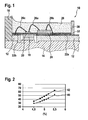
- FIG. 1 a cross section through an inventive component, the corrosion-sensitive areas are protected with a gel layer
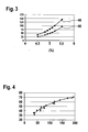
- FIG. 2 a correlation between the concentration of the hardener in the gel in% by weight and the resulting Shore00 hardness of the cured gel as a function of the processing temperature
- FIG. 3 a correlation between the concentration of the hardener in the Gel in% by weight and the force to be used in a measurement of the cured gel with a texture analyzer depending on the processing temperature
- FIG. 4 a correlation of the force determined by a texture analyzer and the corresponding Shore00 hardness of the gel.
- FIG. 1 an inventive electronic component in the form of a regulator 10 according to a first embodiment of the present invention is shown.
- the controller 10 comprises a substrate 12, which is made for example of a ceramic material or of a suitable polymeric material such as PET.
- the substrate 12 is arranged on a heat sink 14, which serves to dissipate heat energy arising and is made of a suitable, for example, metallic material.
- the heat sink 14 is in contact with a housing 16, which simultaneously acts as a boundary of the substrate 12.
- the substrate 12 is part of the housing 16.
- a heat-conducting layer 18 is provided, on which a circuit 20, preferably an integrated circuit is located.
- a circuit 20 preferably an integrated circuit is located.
- contact tracks 22a, 22b are further provided, which serve the electrical contacting of the electronic components of the component 10.
- the micromechanical sensor element may, for example, be designed as a pressure sensor.
- the circuit 20 and the additional substrate 24 are contacted with each other, for example, by a first bonding wire 26a.
- the additional substrate 24 is electrically contacted via a second bonding wire 26b to the contact track 22a.
- the circuit 20 is also connected to the contact track 22b by a third bonding wire 26c.
- the circuit 20 serves, for example, for controlling, measured value detection and evaluation of the electronic component in the form of the additional substrate 24.
- the component 10 furthermore has a gel layer 28 which covers the substrate 12 on its side facing away from the heat sink 14 at least in regions.
- the gel layer 28 is bounded laterally by the housing 16 and an overflow 30 spatially in its extension.
- the layer thickness of the gel is preferably dimensioned so that all corrosion-sensitive electronic components such as the circuit 20 and the additional substrate 24 are enclosed by the gel layer 28.
- the gel layer 28 is preferably made on the basis of a vinyl-modified polydimethylsiloxane.
- the gel layer 28 is preferably produced in such a way that a gel based on a suitable polysiloxane is introduced into the cavity formed by the housing 16, the substrate 12 and the overflow 30.
- the gel further contains a suitable curing agent based on a polysiloxane having terminal and optionally further hydride groups.
- the gel may, for example, be designed as a two-component system and have the following exemplary composition: Component A - Vinyl-containing base polymer about 98-99% by weight - bonding agent about 1% by weight - platinum catalyst (organometallic compound) about 0.5% by weight of a Pt-containing stock solution - Inhibitor ⁇ 1% by weight Component B - Vinyl-containing base polymer approx. 84 - 94 wt.% - bonding agent about 1% by weight - Harder about 5 - 15 wt.%
- the gel may further contain fillers, such as finely divided silica as a thixotropic agent or silica gel or aluminum oxides.
- the gel layer 28 Since the gel layer 28 is in direct contact with electronic components, the gel must have high ionic purity, particularly with respect to its potassium, sodium, lithium, chloride or bromide content, to avoid contact corrosion and associated electrical faults.
- the gel is crosslinked at temperatures of 120 to 180 ° C in an oven via a platinum-catalyzed hydrosilylation reaction.
- the concentration of the hardener in the gel is selected so that the resulting gel layer 28 after curing has a Shore00 hardness of 30 to 50, preferably from 40 to 48 points.
- FIG. 2 shows a plot of the achievable Shore00 hardness of the cured gel over the concentration of hardener contained in the gel in wt.%
- the gel hardness measurement via the Texture Analyzer measures the force required to allow a specimen to penetrate a certain distance into the sample to be examined.
- This type of measurement of the so-called texture of the specimen is used primarily in the food industry and responds to differences in specimens such as e.g. Layer thickness variances, shape and material as well as influences due to wall or floor effects of the measuring tank are very sensitive. For the comparability of the measurements, therefore, the same test specimens with a uniform layer thickness (ie filling quantity) must be used.
- curve 46 shows, analogous to curve 40, the achievable hardness if the curing of the gel is carried out for one hour at 120 ° C. and curve 48 is analogous to curve 42 the achievable hardness when the gel is cured for two hours at a temperature of 150 ° C.
- FIG. 4 shows a correlation of hardness values obtained via a texture analyzer with the corresponding Shore00 hardness.
- the gel used contains an adhesion promoter, suitable compounds being, in particular, compounds which on the one hand have an alkoxy group and, on the other hand, vinyl or Si-H groups, so that they have the necessary bifunctional character to be firmly bound both in the three-dimensional polymeric siloxane network of the gel layer 28 and at the same time have a good adhesion with the materials of the substrate 12 and the housing 16 or the overflow 30.
- suitable compounds being, in particular, compounds which on the one hand have an alkoxy group and, on the other hand, vinyl or Si-H groups, so that they have the necessary bifunctional character to be firmly bound both in the three-dimensional polymeric siloxane network of the gel layer 28 and at the same time have a good adhesion with the materials of the substrate 12 and the housing 16 or the overflow 30.
- alkylvinylsiloxanes or silanes with glycidoxy or alkoxy termination, glycidoxypropyltrialkoxysilanes, silylated polyglycols or derivatives of these compounds are suitable as adhesion promoters.
- the substrate 12 may be provided with a primer layer 32 prior to application of the gel layer 28.
- the gel layer 28 produced in this way is suitable for use temperatures between -45 and 150 degrees Celsius and also withstands dynamic loads, such as, for example, a sine-shaker test in the frequency range from 100 to 1000 Hz with an amplitude of 0.19 mm and a maximum acceleration of 300 m / s 2 occur as well as the loads in so-called random-vibration investigations with a maximum acceleration of up to 800 m / s 2 .
- dynamic loads such as, for example, a sine-shaker test in the frequency range from 100 to 1000 Hz with an amplitude of 0.19 mm and a maximum acceleration of 300 m / s 2 occur as well as the loads in so-called random-vibration investigations with a maximum acceleration of up to 800 m / s 2 .
Landscapes
- Engineering & Computer Science (AREA)
- Power Engineering (AREA)
- Microelectronics & Electronic Packaging (AREA)
- Chemical & Material Sciences (AREA)
- Dispersion Chemistry (AREA)
- Physics & Mathematics (AREA)
- Condensed Matter Physics & Semiconductors (AREA)
- General Physics & Mathematics (AREA)
- Computer Hardware Design (AREA)
- Structures Or Materials For Encapsulating Or Coating Semiconductor Devices Or Solid State Devices (AREA)
- Non-Metallic Protective Coatings For Printed Circuits (AREA)
- Micromachines (AREA)
Description
Die Erfindung betrifft ein elektronisches Bauteil und ein Verfahren zu dessen Herstellung sowie dessen Verwendung nach dem Oberbegriff der unabhängigen Ansprüche.The invention relates to an electronic component and a method for its production and its use according to the preamble of the independent claims.
Bei elektrischen bzw. elektronischen Bauteilen für Kraftfahrzeuganwendungen ist ein wirksamer Schutz der darin enthaltenen Schaltungselemente insbesondere vor korrosiven Witterungseinflüssen unabdingbar. Aus diesem Grund werden elektronische Bauteile beispielsweise mit Gelen auf der Basis von Polysiloxanen zum Schutz vor korrosiven Umwelteinflüssen versiegelt. Ein Verfahren zur Herstellung derartiger Versiegelungen ist beispielsweise aus der
Derartige Gelsysteme erfüllen jedoch nicht das Anforderungsprofil von Bauteilen, die sowohl starken dynamischen Belastungen als auch hohen Temperaturdifferenzen ausgesetzt sind. Um Temperaturwechselbeanspruchungen gerecht zu werden, zeigen handelsübliche Gelsysteme meist ein Härtefenster im Penetrationsbereich. Die Penetration ist dabei ein Maß für die Konsistenz bzw. Verformbarkeit des Gelsystems und gibt an, um welche Strecke ein Kegel bestimmter Abmessung senkrecht in das betreffende Gel unter vorgeschriebenen Bedingungen gemäß DIN 51804 eindringt.However, such gel systems do not meet the requirement profile of components that are exposed both strong dynamic loads and high temperature differences. To meet thermal cycling, commercial gel systems usually show a hardness window in the penetration area. The penetration is a measure of the consistency or deformability of the gel system and indicates the distance by which a cone of certain dimensions penetrates vertically into the relevant gel under prescribed conditions according to DIN 51804.
Gelsysteme, deren Härte diesem Härtebereich zuzuordnen ist, neigen bei Schüttelbelastungen zu starken Gelbewegungen, die die zu schützende Elektronik (Chips, Bonddrähte) schädigt und speziell bei Bonddrähten zu sogenannten Fersenbrüchen führt. Außerdem zeigen derartige Gelsysteme unbefriedigende Härtestabilitäten bei auftretenden Hochtemperatur-Beanspruchungen. Als Konsequenz können Bauteile mit weichen Gelen, deren Härte im Penetrationsbereich liegt, nicht vollständig mit Gel bedeckt werden oder nur mit einer relativ dünnen Gelschicht überzogen werden. Sie bleiben somit für korrosive Medien angreifbar.Gel systems, the hardness of which is assigned to this hardness range, tend with shaking loads to strong gel movements, which damage the electronics to be protected (chips, bonding wires) and leads to so-called heel breaks especially with bonding wires. In addition, such gel systems show unsatisfactory hardness stabilities in the event of high-temperature stresses. As a consequence, components with soft gels, whose hardness is in the penetration range, can not be completely covered with gel or only coated with a relatively thin layer of gel. They remain vulnerable to corrosive media.
Aufgabe der vorliegenden Erfindung ist es, ein elektronisches Bauteil bereitzustellen, das einen kostengünstigen und wirkungsvollen Schutz gegenüber Umwelteinflüssen auch bei Temperatur- oder Schüttebelastungen aufweist.Object of the present invention is to provide an electronic component, which has a cost effective and effective protection against environmental influences, even with temperature or Schüttebelastungen.
Das erfindungsgemäße Bauteil bzw. das Verfahren zu dessen Herstellung gemäß den kennzeichnenden Merkmalen der unabhängigen Ansprüche hat gegenüber dem Stand der Technik den Vorteil, dass korrosionsempfindliche Bereiche des Bauteils mit einer geeigneten Gelbeschichtung so versiegelt sind, dass eine Einwirkung von Witterungseinflüssen auf die geschützten Bereiche verhindert wird und diese Schutzwirkung auch bei hohen thermischen und mechanischen Belastungen erhalten bleibt. Dies wird erreicht, indem das erfindungsgemäße Bauteil eine Gelschicht aufweist, deren Shore00-Härte in einem Bereich angesiedelt ist, in dem das Gel einerseits keine plastische Verformung unter mechanischen Einflüssen zeigt, andererseits jedoch auch nicht so spröde ist, dass Schüttebelastungen des Bauteils zu Rissen oder Ablösungserscheinungen führen. Dies ist insbesondere in einem Shore00-Härtebereich von 40 bis 48 Punkten der Fall.The component according to the invention or the method for its production according to the characterizing features of the independent claims has the advantage over the prior art that corrosion-sensitive areas of the component are sealed with a suitable gel coating in such a way that an influence of weathering on the protected areas is prevented and this protective effect is maintained even at high thermal and mechanical loads. This is achieved by the component according to the invention comprises a gel layer whose Shore00 hardness is located in a range in which the gel on the one hand shows no plastic deformation under mechanical influences, on the other hand, however, is not so brittle that Schüttebelastungen the component to cracks or Lead to separation phenomena. This is the case in particular in a Shore00 hardness range of 40 to 48 points.
Das mit der Gelschicht versehene Bauteil wird sowohl hohen dynamischen Anforderungen als auch Temperaturwechselbelastungen sowie Hochtemperatur- bzw. Tieftemperaturbeanspruchungen gerecht, ohne dass der Korrosionsschutz für korrosionsempfindliche Bauelemente des Bauteils verloren geht. Durch die Einstellung der Gelhärte in einem mittleren Härtebereich wird ein relativ rigides, dreidimensionales Netzwerk erhalten, das gegenüber dynamischen Belastungen, wie sie beispielsweise beim Einsatz elektronischer Reglerbauteile für Generatoren vorkommen, unempfmdlich reagiert und Bonddrahtfersenbrüche bei Bonddrähten mit einem Durchmesser von über 50 Mikrometer vermieden werden. Das Gel ist weiterhin unempfindlich gegenüber üblicherweise im Motorraum vorkommende Medien wie z. B. Öle, Frostschutzmittel, Benzin, Diesel, Kaltreiniger oder salzhaltige Ablagerungen.The component provided with the gel layer satisfies both high dynamic requirements and thermal cycling as well as high-temperature or low-temperature stresses, without the corrosion protection for corrosion-sensitive components of the component being lost. By setting the gel hardness in a medium hardness range, a relatively rigid, three-dimensional network is obtained, which in contrast to dynamic loads, such as in the case of The use of electronic controller components for generators, reacting unresponsive and avoid bonding wire breakages in bonding wires with a diameter of over 50 microns. The gel is still insensitive to commonly occurring in the engine compartment media such. As oils, antifreeze, gasoline, diesel, cold cleaners or saline deposits.
Vorteilhafte Weiterbildungen der Erfindung ergeben sich aus den in den Unteransprüchen genannten Maßnahmen.Advantageous developments of the invention will become apparent from the measures mentioned in the dependent claims.
So ist es vorteilhaft, wenn die Gelschicht auf der Basis eines Polydimethylsiloxans, eines Polyurethans oder eines Epoxidharzes ausgeführt ist, da diese Materialien besonders robust und medienbeständig sind. Besonders geeignet sind Gelsysteme auf der Basis von vinylgruppenmodifizierten Polydimethylsiloxanen.Thus, it is advantageous if the gel layer is based on a polydimethylsiloxane, a polyurethane or an epoxy resin, since these materials are particularly robust and resistant to media. Especially suitable are gel systems based on vinyl group-modified polydimethylsiloxanes.
Ein weiterer besonderer Vorteil der anspruchsgemäßen Gelschicht ist es, dass auch größere Schichtdicken der Gelschicht von mehr als 3 µm realisiert werden können, ohne dass im Dauerbetrieb Risse oder Ablösungserscheinungen auftreten.Another particular advantage of the claimed gel layer is that even greater layer thicknesses of the gel layer of more than 3 μm can be realized without cracks or detachment phenomena occurring in continuous operation.
In einer besonders vorteilhaften Ausführungsform ist zwischen dem Substrat und der Gelschicht eine Schicht aus einem Haftvermittler vorgesehen, sodass es zu einer besonders stabilen Anbindung der Gelschicht an das zu schützende Substrat kommt. Vorteilhafter Weise wird die Haftvermittlerschicht auf der Basis eines Alkylvinylsiloxans mit Glycidoxy- oder Alkoxyterminierung, eines bifunktionellen Silans wie beispielsweise eines Glycidoxyalkyltrialkoxysilans oder eines silylierten Polyglycols ausgeführt.In a particularly advantageous embodiment, a layer of an adhesion promoter is provided between the substrate and the gel layer, so that a particularly stable attachment of the gel layer to the substrate to be protected is achieved. Advantageously, the primer layer is based on an alkylvinylsiloxane having glycidoxy or alkoxy termination, a bifunctional silane such as a glycidoxyalkyltrialkoxysilane or a silylated polyglycol.
Ein Ausführungsbeispiel der ErFmdung ist in der Zeichnung dargestellt und in der nachfolgenden Beschreibung näher erläutert. Es zeigt
In
Auf dem Kühlkörper 14 ist weiterhin, vorzugsweise in einer Durchbrechung des Substrates 12, eine wärmeleitende Schicht 18 vorgesehen, auf der sich eine Schaltung 20, vorzugsweise eine integrierte Schaltung befmdet. Auf dem Substrat 12 sind weiterhin Kontaktbahnen 22a, 22b vorgesehen, die der elektrischen Kontaktierung der elektronischen Bauelemente des Bauteils 10 dienen. Weiterhin ist auf dem Substrat 12 ein Zusatzsubstrat 24 beispielsweise aus einer Aluminiumoxidkeramik angeordnet, das beispielsweise als elektronischer Regler oder mikromechanisches Sensorelement ausgeführt ist. Das mikromechanische Sensorelement kann bspw. als Drucksensor ausgeführt sein. Die Schaltung 20 und das Zusatzsubstrat 24 sind beispielsweise durch einen ersten Bonddraht 26a miteinander kontaktiert. Weiterhin ist das Zusatzsubstrat 24 über einen zweiten Bonddraht 26b mit der Kontaktbahn 22a elektrisch kontaktiert. Die Schaltung 20 ist darüber hinaus mit einem dritten Bonddraht 26c mit der Kontaktbahn 22b verbunden.On the
Dabei dient die Schaltung 20 beispielsweise der Ansteuerung, Messwerterfassung und -auswertung des elektronischen Bauelements in Form des Zusatzsubstrats 24.In this case, the
Des Bauteils 10 weist weiterhin eine Gelschicht 28 auf, die das Substrat 12 auf seiner dem Kühlkörper 14 abgewandten Seite zumindest bereichsweise bedeckt. Die Gelschicht 28 wird seitlich durch das Gehäuse 16 sowie einen Überlauf 30 räumlich in ihrer Ausdehnung begrenzt. Die Schichtdicke des Gels ist vorzugsweise so bemessen, dass alle korrosionsempfindlichen elektronischen Bauelemente wie die Schaltung 20 bzw. das Zusatzsubstrat 24 von der Gelschicht 28 umschlossen sind. Gleiches gilt für die Bonddrähte 26a - 26c. Die Gelschicht 28 ist vorzugsweise auf der Basis eines mit Vinylgruppen modifizierten Polydimethylsiloxans ausgeführt. Die Herstellung der Gelschicht 28 erfolgt vorzugsweise so, dass ein Gel auf der Basis eines geeigneten Polysiloxans in die durch das Gehäuse 16, das Substrat 12 und den Überlauf 30 gebildete Kavität eingefüllt wird. Das Gel enthält weiterhin einen geeigneten Härter auf der Basis eines Polysiloxans, das terminale und gegebenenfalls weitere Hydridgruppen aufweist.The
Das Gel kann beispielsweise als Zweikomponentensystem ausgeführt sein und folgende beispielhafte Zusammensetzung aufweisen:
Das Gel kann weiterhin Füllstoffe enthalten, wie beispielsweise hochdisperse Kieselsäure als Thixotropierungsmittel oder Silikagel bzw. Aluminiumoxide.The gel may further contain fillers, such as finely divided silica as a thixotropic agent or silica gel or aluminum oxides.
Da die Gelschicht 28 in direktem Kontakt mit elektronischen Bauelementen steht, muss das Gel eine hohe Ionenreinheit insbesondere bezüglich seines Kalium-, Natrium-, Lithium-, Chlorid- oder Bromidgehaltes aufweisen, um Kontaktkorrosion und damit verbundene elektrische Fehler zu vermeiden.Since the
In einem nachgeschalteten Aushärteschritt wird das Gel bei Temperaturen von 120 bis 180 °C in einem Ofen über eine Platin-katalysierte Hydrosilylierungsreaktion vernetzt.In a subsequent curing step, the gel is crosslinked at temperatures of 120 to 180 ° C in an oven via a platinum-catalyzed hydrosilylation reaction.
Um eine ausreichend schüttelfeste und temperaturwechselstabile Gelschicht 28 zu erzielen, wird die Konzentration des Härters im Gel so gewählt, dass die resultierende Gelschicht 28 nach der Aushärtung eine Shore00-Härte von 30 bis 50, vorzugsweise von 40 bis 48 Punkten aufweist.In order to achieve a sufficiently shaky and temperature-
Mittels der in
Bei der Gelhärtemessung über den Texture Analyser wird die Kraft gemessen, die nötig ist, um einen Probekörper eine bestimmte Distanz in die zu untersuchende Probe eindringen zu lassen. Diese Art der Messung der sogenannten Textur des Probekörpers wird vor allem in der Lebensmittelindustrie eingesetzt und reagiert auf Unterschiede der Probekörper wie z.B. Schichtdickenvarianzen, Form und Material sowie Einflüsse durch Wand- oder Bodeneffekte des Messbehälters sehr sensibel. Zur Vergleichbarkeit der Messungen müssen daher die gleichen Probekörper mit einer einheitlichen Schichtdicke (also Füllmenge) eingesetzt werden.The gel hardness measurement via the Texture Analyzer measures the force required to allow a specimen to penetrate a certain distance into the sample to be examined. This type of measurement of the so-called texture of the specimen is used primarily in the food industry and responds to differences in specimens such as e.g. Layer thickness variances, shape and material as well as influences due to wall or floor effects of the measuring tank are very sensitive. For the comparability of the measurements, therefore, the same test specimens with a uniform layer thickness (ie filling quantity) must be used.
Die Kurve 46 zeigt analog zu Kurve 40 die erreichbare Härte wenn die Aushärtung des Gels über eine Stunde bei 120 °C durchgeführt wird und Kurve 48 analog zu Kurve 42 die erreichbare Härte, wenn das Gel über zwei Stunden bei einer Temperatur von einer 150 °C ausgehärtet wird.
Um eine bessere Anbindung der Gelschicht 28 an das Substrat 12 zu erzielen, enthält das verwendete Gel einen Haftvermittler, wobei als Haftvermittler insbesondere Verbindungen geeignet sind, die zum einen eine Alkoxygruppe und andererseits Vinyl-oder Si-H-Gruppen aufweisen, sodass sie den nötigen bifunktionellen Charakter zeigen, um sowohl in das dreidimensionale polymere Siloxannetzwerk der Gelschicht 28 fest eingebunden zu werden und gleichzeitig eine gute Haftung mit den Werkstoffen des Substrates 12 bzw. des Gehäuses 16 oder des Überlaufs 30 aufzuweisen. So sind beispielsweise Alkylvinylsiloxane oder -silane mit Glycidoxy- oder Alkoxyterminierung, Glycidoxypropyltrialkoxysilane, silylierte Polyglycole oder Derrivate dieser Verbindungen als Haftvermittler geeignet. Optional kann das Substrat 12 vor dem Aufbringen der Gelschicht 28 mit einer Haftvermittlerschicht 32 versehen werden.In order to achieve a better bonding of the
Die so erzeugte Gelschicht 28 ist für Einsatztemperaturen zwischen - 45 und 150 Grad Celsius geeignet und hält auch dynamischen Belastungen stand, wie sie beispielsweise bei einer Sinusschüttelprüfung im Frequenzbereich von 100 bis 1000 Hz mit einer Amplitude von 0,19 mm und einer maximalen Beschleunigung von 300 m/s2 auftreten, sowie auch den Belastungen bei sogenannten Random-Vibration-Untersuchungen mit einer maximalen Beschleunigung von bis zu 800 m/s2.The
Alternativ können anstelle der beschriebenen Siloxangele auch vorzugsweise transparente Polyurethanvergussmassen oder Epoxidharze eingesetzt werden.Alternatively, it is also possible to use transparent polyurethane casting compounds or epoxy resins instead of the described siloxane gels.
Claims (10)
- Electronic component, in particular regulator or micromechanical sensor element, comprising a substrate and a housing encompassing the substrate, and also comprising a circuit arranged on the substrate, wherein at least the circuit is provided with a gel layer for protection against ambient influences, wherein the gel layer (28) has a Shore 00 hardness of 30 to 50 points, and wherein the gel of the gel layer (28) contains an adhesion converter.
- Component according to Claim 1, characterized in that the gel layer (28) has a Shore 00 hardness of 40 to 48 points.
- Component according to Claim 1 or 2, characterized in that the gel layer (28) is embodied on the basis of a polydimethylsiloxane, a polyurethane or an epoxy resin.
- Component according to Claim 3, characterized in that the gel layer (28) is embodied on the basis of a vinyl-group-modified polydimethylsiloxane.
- Component according to any of the preceding claims, characterized in that the gel layer (28) has a layer thickness of more than 3 µm.
- Component according to Claim 1, characterized in that the adhesion promoter is an alkylvinylsiloxane
with glycidoxy or alkoxy termination, a glycidoxyalkyltrialkoxysilane or a silylated polyglycol. - Method for producing an electronic or electrical component, in particular regulator or micromechanical sensor element, comprising a substrate and a housing encompassing the substrate, and also comprising a circuit arranged on the substrate, wherein at least the circuit is provided with a gel layer for protection against ambient influences, wherein the Shore 00 hardness of the gel layer is set to a value of 30 to 50 points by way of the amount of a hardener added to the gel, and wherein the gel of the gel layer (28) contains an adhesion promoter.
- Method according to Claim 7, characterized in that a gel based on a polydimethylsiloxane is used as the gel and a hydridic polysiloxane is used as the hardener.
- Method according to Claim 7 or 8, characterized in that the hardener is added to the gel of the gel layer in a concentration of 4.2 to 5.7% by weight.
- Use of a component according to any of Claims 1 to 6 as a regulator for generators or as a micromechanical pressure sensor in motor vehicle applications.
Applications Claiming Priority (4)
| Application Number | Priority Date | Filing Date | Title |
|---|---|---|---|
| DE102004012600 | 2004-03-12 | ||
| DE102004012600 | 2004-03-12 | ||
| DE102004028888A DE102004028888A1 (en) | 2004-03-12 | 2004-06-15 | Electronic component, especially regulator or micromechanical sensor element for automobiles, with gel layer of specific hardness for protecting circuitry against corrosion, temperature and vibration |
| DE102004028888 | 2004-06-15 |
Publications (3)
| Publication Number | Publication Date |
|---|---|
| EP1587140A2 EP1587140A2 (en) | 2005-10-19 |
| EP1587140A3 EP1587140A3 (en) | 2009-04-01 |
| EP1587140B1 true EP1587140B1 (en) | 2011-09-21 |
Family
ID=34938843
Family Applications (1)
| Application Number | Title | Priority Date | Filing Date |
|---|---|---|---|
| EP05101527A Expired - Fee Related EP1587140B1 (en) | 2004-03-12 | 2005-03-01 | Electronic device which accommodates an electronic circuit provided with a gel layer and method for producing said device |
Country Status (1)
| Country | Link |
|---|---|
| EP (1) | EP1587140B1 (en) |
Families Citing this family (3)
| Publication number | Priority date | Publication date | Assignee | Title |
|---|---|---|---|---|
| DE102011077684A1 (en) * | 2011-06-17 | 2012-12-20 | Robert Bosch Gmbh | Cover material for a microchip, microchip with cover material and method for providing such a microchip |
| JP6047954B2 (en) | 2012-07-03 | 2016-12-21 | 株式会社ジェイテクト | Motor unit |
| CN109650328B (en) * | 2018-12-17 | 2020-05-19 | 大连理工大学 | Shock wave base excitation device for dynamic characteristic test and working method thereof |
Family Cites Families (6)
| Publication number | Priority date | Publication date | Assignee | Title |
|---|---|---|---|---|
| JPS6177353A (en) * | 1984-09-25 | 1986-04-19 | Toshiba Corp | Semiconductor rectifier |
| US5165956A (en) * | 1991-09-27 | 1992-11-24 | At&T Bell Laboratories | Method of encapsulating an electronic device with a silicone encapsulant |
| DE69512299T2 (en) * | 1994-04-08 | 2000-05-25 | Shinetsu Chemical Co | Thixotropic fluorosilicone gel composition |
| DE19860035A1 (en) * | 1998-12-23 | 2000-07-06 | Trw Automotive Electron & Comp | Electronics module |
| JP3663120B2 (en) * | 2000-09-04 | 2005-06-22 | 株式会社日立製作所 | Mounting structure and mounting method for automobile engine control unit |
| US6614108B1 (en) * | 2000-10-23 | 2003-09-02 | Delphi Technologies, Inc. | Electronic package and method therefor |
-
2005
- 2005-03-01 EP EP05101527A patent/EP1587140B1/en not_active Expired - Fee Related
Also Published As
| Publication number | Publication date |
|---|---|
| EP1587140A2 (en) | 2005-10-19 |
| EP1587140A3 (en) | 2009-04-01 |
Similar Documents
| Publication | Publication Date | Title |
|---|---|---|
| EP0019135B1 (en) | Measuring probe for use in measuring the temperature or mass of a flowing medium and process for its manufacture | |
| DE102004011203B4 (en) | Method for mounting semiconductor chips and corresponding semiconductor chip arrangement | |
| DE69824363T2 (en) | Curable silicone composition and electronic components | |
| EP0011738B1 (en) | Process for lowering the porosity and surface roughness of a ceramic support and coating composition therefor | |
| DE69736320T2 (en) | ELECTRONIC CONTROL MODULE WITH LIQUID SEALS | |
| DE60223009T2 (en) | ADDITION-SLICED SILICONE COMPOSITION OF BELLOW CONSISTENCY | |
| EP1560010A1 (en) | Load cell with strain gauge with adhesive layer of inorganic-organic hybrid-polymer (ORMOCER) | |
| EP0357717A1 (en) | Manometer. | |
| US6586105B2 (en) | Packaging structure and method for automotive components | |
| DE102005013818A1 (en) | Pressure sensor with integrated temperature sensor | |
| US10519031B2 (en) | Encapsulations for mems sense elements and wire bonds | |
| EP1587140B1 (en) | Electronic device which accommodates an electronic circuit provided with a gel layer and method for producing said device | |
| EP0264635A2 (en) | Electrically conductible adhesive for a large temperature range | |
| EP0096156B1 (en) | Process for the quasi-hermetic, almost reactionless covering of sensitive physical structures, especially strain gauges | |
| DE102004028888A1 (en) | Electronic component, especially regulator or micromechanical sensor element for automobiles, with gel layer of specific hardness for protecting circuitry against corrosion, temperature and vibration | |
| EP2803082B1 (en) | Electronic component having a corrosion-protected bonding connection and method for producing the component | |
| DE3415772C2 (en) | ||
| DE19736090B4 (en) | Protective layer device and method for producing a protective layer for a device | |
| DE102004033475A1 (en) | Corrosion protection for micromechanical sensor elements, e.g. for a pressure sensor, comprises a passivating agent that at least partially covers electrical components and a material layer applied to the top of the passivator | |
| DE102007032074A1 (en) | Electronic components encapsulating electronic housing therein | |
| DE60303643T2 (en) | Curable compositions and electrical / electronic parts | |
| DE10046017B4 (en) | Semiconductor pressure sensor device with sensor chip covered by protective element | |
| DE102018207689B4 (en) | Method for producing at least one membrane arrangement, membrane arrangement for a micromechanical sensor and component | |
| DE19518027C2 (en) | Process for the precise spacing encasing of components provided with functional layers and components produced thereafter | |
| DE102007042976A1 (en) | Pressure sensor for determining pressure of hot or aggressive fluid media i.e. exhaust gas stream, in motor vehicle, has diaphragm with plastic connection and coated with additional material layer containing metalliferous components |
Legal Events
| Date | Code | Title | Description |
|---|---|---|---|
| PUAI | Public reference made under article 153(3) epc to a published international application that has entered the european phase |
Free format text: ORIGINAL CODE: 0009012 |
|
| AK | Designated contracting states |
Kind code of ref document: A2 Designated state(s): AT BE BG CH CY CZ DE DK EE ES FI FR GB GR HU IE IS IT LI LT LU MC NL PL PT RO SE SI SK TR |
|
| AX | Request for extension of the european patent |
Extension state: AL BA HR LV MK YU |
|
| PUAL | Search report despatched |
Free format text: ORIGINAL CODE: 0009013 |
|
| AK | Designated contracting states |
Kind code of ref document: A3 Designated state(s): AT BE BG CH CY CZ DE DK EE ES FI FR GB GR HU IE IS IT LI LT LU MC NL PL PT RO SE SI SK TR |
|
| AX | Request for extension of the european patent |
Extension state: AL BA HR LV MK YU |
|
| 17P | Request for examination filed |
Effective date: 20091001 |
|
| 17Q | First examination report despatched |
Effective date: 20091110 |
|
| AKX | Designation fees paid |
Designated state(s): DE FR GB |
|
| REG | Reference to a national code |
Ref country code: DE Ref legal event code: R079 Ref document number: 502005011906 Country of ref document: DE Free format text: PREVIOUS MAIN CLASS: H01L0023240000 Ipc: H02K0011000000 |
|
| GRAP | Despatch of communication of intention to grant a patent |
Free format text: ORIGINAL CODE: EPIDOSNIGR1 |
|
| RIC1 | Information provided on ipc code assigned before grant |
Ipc: H01L 23/24 20060101ALI20110511BHEP Ipc: H02K 19/36 20060101ALI20110511BHEP Ipc: H02K 11/00 20060101AFI20110511BHEP |
|
| RIN1 | Information on inventor provided before grant (corrected) |
Inventor name: REYES TELLO, LAURA Inventor name: HOLST, MARCO Inventor name: BACHMANN, STEFAN Inventor name: FISCHER, ERWIN |
|
| GRAS | Grant fee paid |
Free format text: ORIGINAL CODE: EPIDOSNIGR3 |
|
| GRAA | (expected) grant |
Free format text: ORIGINAL CODE: 0009210 |
|
| AK | Designated contracting states |
Kind code of ref document: B1 Designated state(s): DE FR GB |
|
| REG | Reference to a national code |
Ref country code: GB Ref legal event code: FG4D Free format text: NOT ENGLISH |
|
| REG | Reference to a national code |
Ref country code: DE Ref legal event code: R096 Ref document number: 502005011906 Country of ref document: DE Effective date: 20111117 |
|
| PLBE | No opposition filed within time limit |
Free format text: ORIGINAL CODE: 0009261 |
|
| STAA | Information on the status of an ep patent application or granted ep patent |
Free format text: STATUS: NO OPPOSITION FILED WITHIN TIME LIMIT |
|
| 26N | No opposition filed |
Effective date: 20120622 |
|
| REG | Reference to a national code |
Ref country code: DE Ref legal event code: R097 Ref document number: 502005011906 Country of ref document: DE Effective date: 20120622 |
|
| PGFP | Annual fee paid to national office [announced via postgrant information from national office to epo] |
Ref country code: FR Payment date: 20130329 Year of fee payment: 9 Ref country code: GB Payment date: 20130318 Year of fee payment: 9 |
|
| PGFP | Annual fee paid to national office [announced via postgrant information from national office to epo] |
Ref country code: DE Payment date: 20140523 Year of fee payment: 10 |
|
| GBPC | Gb: european patent ceased through non-payment of renewal fee |
Effective date: 20140301 |
|
| REG | Reference to a national code |
Ref country code: FR Ref legal event code: ST Effective date: 20141128 |
|
| PG25 | Lapsed in a contracting state [announced via postgrant information from national office to epo] |
Ref country code: FR Free format text: LAPSE BECAUSE OF NON-PAYMENT OF DUE FEES Effective date: 20140331 Ref country code: GB Free format text: LAPSE BECAUSE OF NON-PAYMENT OF DUE FEES Effective date: 20140301 |
|
| REG | Reference to a national code |
Ref country code: DE Ref legal event code: R119 Ref document number: 502005011906 Country of ref document: DE |
|
| PG25 | Lapsed in a contracting state [announced via postgrant information from national office to epo] |
Ref country code: DE Free format text: LAPSE BECAUSE OF NON-PAYMENT OF DUE FEES Effective date: 20151001 |